

Page 1

8xC251TA, 8xC251TB,
8xC251TP, 8xC251TQ,
Hardware Description
Addendum to the 8xC251SA, 8xC251SB,
8xC251SP, 8xC251SQ, User’s Manual
Release Date: November, 1997
Order Number: 273138-001
The 8xC251Tx m ay contain desig n defects or er rors known as errata which may cause
the product to deviate from published specifications. Such errata are not covered by
Intel’s warranty. Current characterized errata are available on request.
Page 2

Information in this document is provided in connection with Intel products. No license, express or implied, by
estopp el or otherwise, to any intellectual p roperty rights is granted by this document. Except as provided in In tel’s
Terms and Cond it ions of S ale f or suc h pro duct s, In tel a ssu mes no liabi li ty wh atso ever, and Inte l d iscla ims any
express or implied warranty, relating to sale and/or use of Intel products including liability or warranties relating to
fitness for a parti cular purpose, m erchantability, or infring ement of any pate nt, copyright or other intellectual
prope rty righ t. Inte l pr oduc ts are not int ende d fo r use in med ical , life s avin g, or lif e sus taini ng ap plic ation s. Intel
may make changes to specifications and product descripti ons at any time, without notice. Contact y our loca l Intel
sales of fice or your distributor to obt ain the latest specifications and before placing your product order .
Designers must not rely on the absence or characteristics of any features or instructions marked "reserved" or
"undef ined ." Inte l res erve s the se for fu ture de finit ion and sh all ha ve no respo nsib ility whats oeve r for c onfli cts o r
incompatibilities arising from future changes to them.
The 8x C251Tx may co ntain de sign de fect s or err ors kno wn as er rata wh ich ma y cause th e pro duct to d eviate
from published specifications. Current characterized errata are available on request.
Copies of documents which have an ordering number and are referenced in this document, or other Intel
literature, may be obtained from:
Intel Corporation
P.O. Box 5937
Denver C O 8021 7-9808
or call 1-800-548-4725.
Many documents are available for download from Intel’s website at http://www.intel.com.
Copyright © Intel Corporation 1997.
*Third party brands and names ar e the property of their respective owners.
Page 3

8xC251Tx Hardware Description
8xC251TA, 8xC251TB, 8xC251TP, 8xC251TQ, Hardware Description
Addendum to the 8xC251SA, 8xC251SB, 8xC251SP, 8xC251SQ, User’s Manual
1.0 INTRODUCTION TO THE 8xC251Tx
1.1 Comparing the 8xC251Tx and 8xC251Sx........ ............ .. ............ ............ ....................... 1
2.0 SIGNAL SUMMARY
3.0 THE SECOND SERIAL I/O PORT
3.1 Overview........................................................................................................................ 7
3.2 Special Function Register Definitions............................................................................ 9
3.2.1 SCON1 .................................................................................................................... 9
3.2.2 SBUF1 ................................................................................................................... 10
3.2.3 SADDR1 ................................................................................................................ 10
3.2.4 SADEN1 ................................................................................................................ 10
3.2.5 BGCON .................................................................................................................. 10
3.2.6 IE1 ......................................................................................................................... 11
3.2.7 IPH1 ....................................................................................................................... 11
3.2.8 IPL1 ....................................................................................................................... 11
4.0 EXTENDED DATA FLOAT TIMING
4.1 Summary of the Extended Data Float Timing Changes .............................. ................ 12
FIGURES
Figure 1 8xC251Tx Block Diagram .....................................................................................1
TABLES
Table 1. 8xC251Tx Signal Summary . ................................................................................ 2
Table 2. 8xC251Tx Signal Descriptions............................................................................. 3
Table 3. Special Function Register (SFR) Map.................................................................. 6
Table 4. Second Serial I/O Port Signals ... .. .............. ......................... .............. .................. 7
Table 5. Second Serial I/O Port Special Function Registers.............................................. 8
Table 6. SCON1 Special Function Register Definitions..................................................... 9
Table 7. BGCON Special Function Register Definitions .................................................. 10
Table 8. IE1 Special Function Register Definitions.......................................................... 11
Table 9. IPH1 Special Function Register Definitions ....................................................... 11
Table 10. IPL1 Special Function Register Definitions........................................................ 11
Table 11. Interrupt Priority of Second Serial I/O Port......................................................... 11
Table 12. UCONFIG1 bit definitions for the 8xC251Tx......................................... .. ........... 12
Table 13. Summary of the EDF# and WSB#[1:0] Configuration Options........................... 13
III
Page 4

Page 5
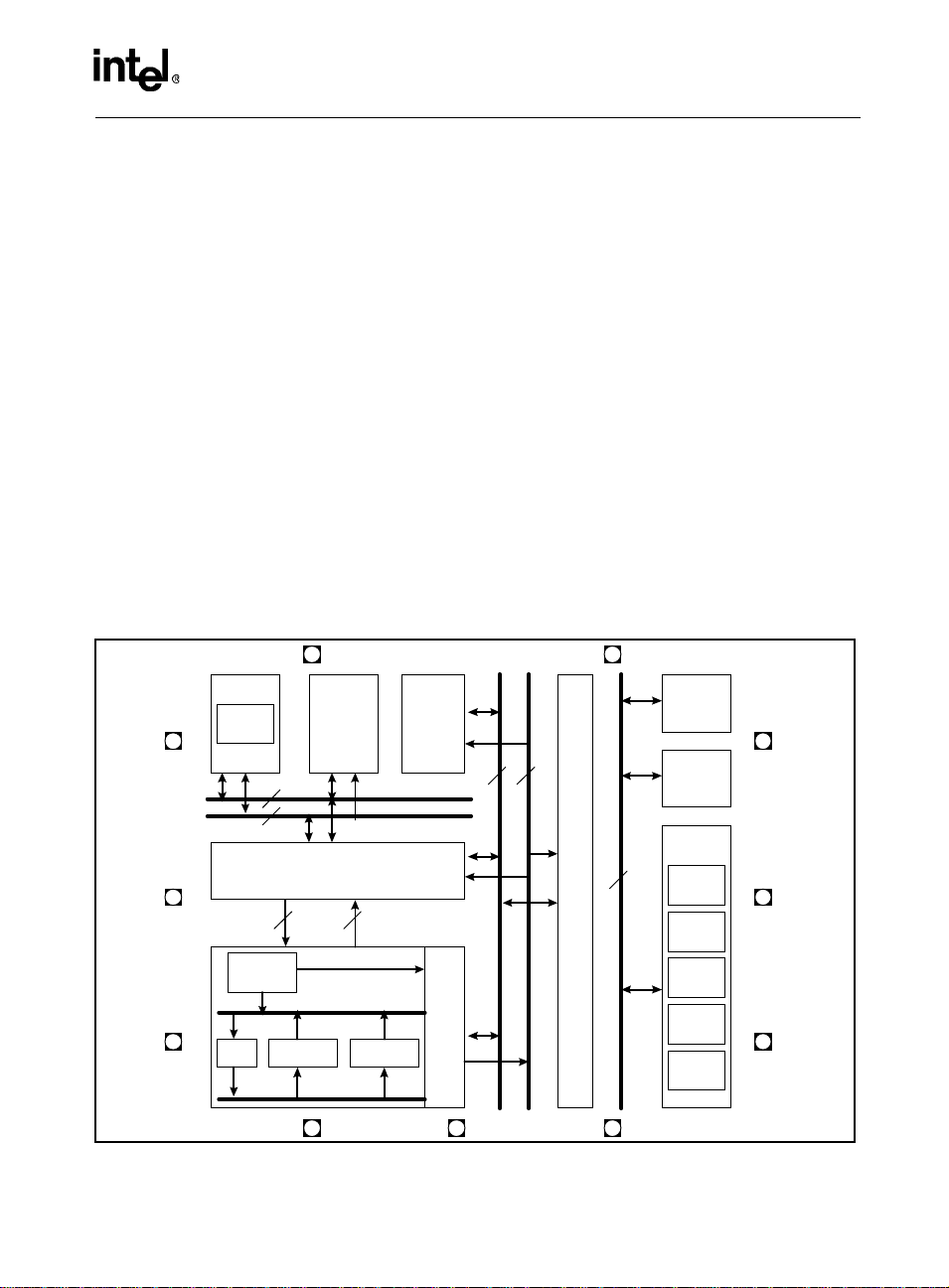
1.0 INTRODUCTION TO THE 8xC251Tx
8xC251Tx Hardware Description
This Ha rdwa re D escr iptio n de scrib es t he 8 xC2 51TA, 8xC 251 TB, 8 xC2 51TP, 8xC 251 TQ (r efer red t o co llec tively as th e 8x C 25 1T x) em b ed ded microc on troller, wh ic h is the ne w e st m em be r of th e MC S
®
251 micro controller family. The 8xC251Tx is pin and code compatible with t he 8xC251Sx but is e nhanced with the addition
of new features.
This document addresses the differences between the two members of the MCS 251 microcontroller family.
For a d e t ai le d de sc r i pti on of the MCS 251 mic ro co ntrolle r c o r e an d s t an d ard peripherals shar ed b y b oth the
8xC251 Sx and 8xC 251Tx, pleas e refer to the
Microc ontroller User’s Manual
(272795).
8xC251SA, 8xC251SB, 8xC251SP, 8xC251SQ Embedded
1.1 Comparing the 8xC251Tx and 8xC251Sx
The di fferences between the 8xC251Tx and the 8xC251Sx are brief ly described here.
• The maximum operating frequency of the 8xC251Tx is 24 Mh z compared to 16 MHz for the 8xC251Sx.
• The 8xC251Tx has two serial I/O ports while the 8xC251Sx has one. The pins for the second serial I/O
port are multiplexed with other functional pins.
• The 8xC251Tx ha s a new configuration option (E xtended Data Float timing) to allow interfac ing with
slower memories. This feature is supported by a bit in the configuration byte, UCONFIG1. Th e corresponding bit in the 8xC251Sx has a different function.
• The 8xC251Tx is offered in with factory programmed ROM while the 8xC251Sx is also offered with
OTPROM/EPROM.
8
RESETP0 (A7-
Clock and
Reset Unit
XTAL2
Interrupt
Handler Unit
Peripherals
IB Bus
3 Timers
XTAL1
P2 (A15-8)
P3
PORT
0-3
16
16
BUS INTE RFACE UNIT
0/D7-0)
EPROM/
ROM
RAM
824
Memory Data
Memory Address
Data Bus
Data Address
PSEN
ALU
16
INSTR
Instruction
Sequencer
24
PC
CPU
SRC1, SRC2
Register
File
Program
Counter
DST
ALE VCC VSS
Data Memory Interface
Figure 1. 8xC251Tx Block Diagram
1
Peripheral Interface Unit
Serial I/O
WDT
PCA
2nd Serial
I/O
P1
Page 6
8xC251Tx Hardware Description
2.0 SIGNAL SUMMARY
Table 1. 8xC251Tx Signal Summary
Address & Data Input/Output
Name PLCC DIP Name PLCC DIP
AD0/P0.0 43 39 P1.0/T2 2 1
AD1/P0.1 42 38 P1.1/T2EX 3 2
AD2/P0.2 41 37
AD3/P0.3 40 36
AD4/P0.4 39 35 P1.4/CEX1 6 5
AD5/P0.5 38 34 P1.5/CEX2 7 6
AD6/P0.6 37 33 P1.6/CEX3/WAIT# 8 7
AD7/P0.7 36 32 P1.7/CEX4/A17/WCLK 9 8
A8/P2.0 24 21 P3.0/RXD 11 10
A9/P2.1 25 22 P3.1/TXD 13 11
A10/P2.2 26 23 P3.4/T0 16 14
A11/P2.3 27 24 P3.51/T1 17 15
A12/P2.4 28 25
A13/P2.5 29 26 Power & Ground
A14/P2.6 30 27 Name PLCC DIP
A15P2.7 31 28 V
P3.7/RD#/A16 19 17 V
P1.7/CEX4/A17/WCLK 9 8 V
Processor Control V
Name PLCC DIP
P3.2/INT0# 14 12 Bus Control & Status
P3.3/INT1# 15 13 Name PLCC DIP
EA# 3531 P3.6/WR# 1816
RST 10 9 P3.7/RD#/A16 19 17
XTAL12118ALE 3330
XTAL2 20 19 PSEN# 32 29
NOTE: Pins in
this font
indicate functions associated with the second serial I/O port.
P1.2/EC/RXD1 4 3
P1.3/CEX0/TXD1 5 4
CC
CC2
SS
V
SS1
SS2
44 40
12
22 20
1
23,24
2
Page 7

8xC251Tx Hardware Description
Table 2. 8xC251Tx Signal Descriptions (Sheet 1 of 3)
Signal
Name
A17 O Address Line 17. Output to memory as the 18th external address bit
A16 O Address Line 16. See RD#. P3.7/RD#
A15:8* O Address Lines. Upper address lines for the external bus. P2.7:0
A7:0 I/O Address/Data Lines. Multiplexed lower address lines and data lines
ALE O Address Latch Enable. ALE signa ls the start of an external bus
CEX0
CEX1
CEX2
CEX3
CEX4
EA# I Ex ternal Access. Direct progr am accesses to on-chip or off-chip
ECI I PCA External Clock Input. External clock input to the 16 bit PCA
INT1:0# I External Interrupts 0 and 1. These inp u ts set IE1:0 in the TC O N
P0.7:0 I/O Port 0. This is an 8 bit, open drain, bidirectional I /O port. AD7:0
P1.0
P1.1
P1.2
P1.3
P1.4
P1.5
P1.6
P1.7
P2.7:0 I/O Port 2. This is an 8 bit, bidirectional I/O port with internal pullups. A15:8
* The descriptions of A15:8/P2.7:0 and AD7:0/P0.7:0 are for non page mode configuration. If configured in
page mode, Port 0 carries the lower address bits (A7:0) and Port 2 carries the upper address bits (A15:8)
and the data (D7:0)
Type Description
(A17) in extended bus applications, depending on the values of bits
RD0 and RD1 in configuration byte UCONFIG0 (see Chapter 4,
"Device Configuration," of the
8xC251SQ Embedded Microcontroller User’s Manual
also RD# and PSEN#.
for external bus.
cycle and indicates that valid address information is available on lines
A15:8 and A7:0. An external latch can use ALE to demultiplex the
address from the address/data bus.
I/O Programmable Counter Array (PCA) input/output pins. These are
input signals for the PCA capture mo de and outp ut signals for the
PCA compare mode and PCA PWM mode.
code mem ory. For EA# = 0, all program memory accesses are off
chip. For EA# = 1, all program memory accesses are on-chip if the
address is within the range of the on-chip program memory; otherwise the access is off-chip. The value of EA# is latched at reset. For
device s without on-chip program memo ry, EA# must be strapped to
ground.
timer.
register. If bits IT1:0 in the TCON register are set, units IE1:0 are set
by the falling edge on the INT1#/INT0#. If bits IT1:0 are clear, bits
IE1:0 are set by a low level on INTO1:0#.
I/O Port 1. This is an 8 bit, bidirectional I/O port with internal pullups. T2
8xC251SA, 8xC251SB, 8xC251SP,
(272795). See
Alternate
Function
P1.7/CEX4/
WCLK
P0/7:0
P1.3/TXD1
P1.4
P1.5
P1.6/WAIT#
P1.7/A17/
WCLK
P1.2/RXD1
P3.3:2
T2EX
ECI/RXD1
CEX0/TXD1
CEX1
CEX2
CEX3/WAIT#
CEX4/A17/
WCLK
3
Page 8

8xC251Tx Hardware Description
Table 2. 8xC251Tx Signal Descriptions (Sheet 2 of 3)
Signal
Name
P3.0
P3.1
P3.2
P3.3
P3.4
P3.5
P3.6
Type Description
I/O Port 3. This is an 8 bit, bidirectional I/O port with internal pullups RXD
P3.7
PSEN# O Program Store Enable. Read signal output to external memory.
Asserted for the address range specified by the configuration byte
Alternate
Function
TXD
INT0#
INT1#
T0
T1
WR#
RD#/A16
UCONFIG0, bits RD1:0.
RD# O Read. Read signal output to external memory. Asserted for the
address range sp ecified by the configuration byte UCONFIG0, bits
P3.7/A16
RD1:0.
RST I Reset. Reset input to the chip. Holding this pin high for 64 oscillator
RXD I/O Receive Serial Data. RXD send and receives dat a in serial I/O mode
periods while the oscillator is running resets the device. The port pins
are driven to their reset conditions when a voltage greater than VIH1
is applied, whether or not the oscillator is running. This signal has a
Schmitt trigger input. Connecting the RST pin to V
capacitor provides power-on reset. Asserting RST when the chip is in
idle mode or powerdown mode returns the chip to normal operation.
through a
CC
P3.0
0 and receives data in serial I/O modes 1, 2 and 3.
RXD1 I/O Receive Serial Data 1. RXD send and receives data in serial I/O
mode 0 and receives data in s erial I/O modes 1, 2 and 3 for the s ec-
P1.2/ECI
ond serial I/O port.
T1:0 I Timer 1:0 External Clock Inputs. When Timer 1:0 operates as a
T2 I/O Timer 2 Clock Input/Output. For Timer 2 capture mode, this signal
T2EX I Timer 2 External Input. In Timer 2 capture mode, a falling edg e ini-
counter, a falling edge on the T1:0 pin increments the count.
is the external clock input. For the clock-out mode, it is the timer 2
clock input.
tiates a capture of Timer 2 registers. In auto-reload mode, a falling
edge causes the Timer 2 registers to be reloaded. In the up-down
P3.5:4
P1.0
P1.1
counter mode, this signal determines the count direction:
•1=up
•0 = down.
TXD O Transmit Serial Data. TXD outputs the shift clock in serial I/O mode
0 and transmits serial data in serial I/O modes 1, 2 and 3.
TXD1 O Transmit Serial Data 1. TXD outputs the shift clock in serial I/O
mode 0 and transmits serial data in serial I/O modes 1, 2 and 3 for
the second serial I/O port.
V
CC
* The descriptions of A15:8/P2.7:0 and AD7:0/P0.7:0 are for non page mode configuration. If configured in
page mode, Port 0 carries the lower address bits (A7:0) and Port 2 carries the upper address bits (A15:8)
PWR Supply Voltage. Connect this pin to the +5 su pply voltage.
P3.1
P1.3/CEX0
and the data (D7:0)
4
Page 9

8xC251Tx Hardware Description
Table 2. 8xC251Tx Signal Descriptions (Sheet 3 of 3)
Signal
Name
V
CC2
V
SS
V
SS1
V
SS2
WAIT# I Real-time Wait State Input. The re al- t ime W AI T# i n pu t is en ab le d b y
Type Description
PWR Secondary Supply Voltage 2. This supply volt ag e co nnect i on is pro-
vided t o reduce p ower supply noise. Connection of this s pin to the
+5V supply voltage is recommended. However, when using the ZX3
as a pin for pin replacement for the 8XC51FX , V
necte d without loss of compatibility (Not available on DIP).
can be unc on -
CC2
GND Circuit Gr oun d. Connect this pin to ground.
GND Seconda r y Gro und . This ground is provided to reduce ground
bounce and improve power supply bypassing. Connection of this pin
to ground is recommended. However, when using the ZX3 as a pin
for pin replacement for the 8XC51FX, V
out loss of compatibility. (Not available in DIP ).
GND Secondary Ground 2. This ground is provided to re duce ground
bounce and improve power supply bypassing. Connection of this pin
to ground is recommended. However, when using the ZX3 as a pin
for pin replacement for the 8XC51FX, V
out loss of compatibility. (Not available in DIP ).
writing a logical "1" to the WCON.0 (RTWE) bit at S:A7H. During bus
cycles, the external memory system can signal ‘system ready’ to the
can be unconnected with-
SS1
can be unconnected with-
SS1
Alternate
Function
P1.6/CEX3
microprocessor in real time by controlling the WAIT# input signal
WCLK O Wait Clock Output. The r eal-time Wait Clock output is d riven b y writ-
ing a logical "1" to the WCON .1 (RTWCE) bit at S:A7H. When
enabled, the WCLK output produces a square wave signal with a
period of one-half the os cillato r frequency
WR# O Write. Write signal output to external memory. Asserted for the mem-
ory address range specified by configuration byte UCONFIG0, bits
RD1:0.
P1.7/CEX4/
A17
P3.6
XTAL1 I Input to On-chip, Inver ti ng Osc illa tor A mp lifi er. To use the inter-
nal oscillator, a crystal/resonator circuit is connected to this pin. If an
external oscillator is used, its output is connected to this pin. XTAL1
is the clock source for the internal timing
XTAL2 O Output of the On-chip, Inverting Oscillator Amplifier. To use the
* The descriptions of A15:8/P2.7:0 and AD7:0/P0.7:0 are for non page mode configuration. If configured in
page mode, Port 0 carries the lower address bits (A7:0) and Port 2 carries the upper address bits (A15:8)
and the data (D7:0)
intern al o sci lla to r, a c r yst al/ r es onat or c irc ui t is co nnect e d t o thi s p in . If
an external oscillator is used, leave XTAL2 unconnected.
5
Page 10

8xC251Tx Hardware Description
Table 3. Special Function Register (SFR) Map
F8
F0 B
00000000
E8 CL
E0 ACC
00000000
D8 CCON
00x00000
D0 PSW
00000000
C8 T2CON
00000000
C0
B8 IPL0
x000 00 00
B0 P3
11111111
A8 IE0
00000000
A0 P2
11111111
98 SCON
00000000
90 P1
11111111
88 TCON000
00000
80 P0
11111111SP00000111
NOTE: Regist ers i n
port.
CH00000
00000000
CMOD
00xxx000
PSW1
00000000
T2MOD
xxxxxx00
SADEN
00000000
IE1
xxxxxxx0
SADDR
00000000
SBUF
xxxxxxxx
TMOD
00000000
000
this font
CCAP0Hx
xxxxxxx
CCAP0L
xxxxxxxx
CCAPM0
x0000000
RCAP2L
00000000
SADEN1
00000000
IP1L
xxxxxxx0
SADDR1
00000000
SCON1
00000000
TL0
00000000
DPL
00000000
are special functions registers that are associated with the second serial I/O
CCAP1Hx
xxxxxxx
CCAP1L
xxxxxxxx
CCAPM1
x0000000
RCAP2H
00000000
IP1H
xxxxxxx0
SBUF1
xxxxxxxx
TL1
00000000
DPH
00000000
CCAP2Hx
xxxxxxx
CCAP2L
xxxxxxxx
CCAPM2
x0000000
TL2
00000000
TH0
00000000
DPXL
00000001
CCAP3Hx
xxxxxxx
CCAP3L
xxxxxxxx
CCAPM3
x0000000
TH2
00000000
TH1
00000000
CCAP4Hx
xxxxxxx
CCAP4L
xxxxxxxx
CCAPM4
x00000 00
SPH
00000000
WDTRST
xxxxxxxx
IPH0
x000 00 00
WCON
xxxxxxxx
BGCON
0000xxxx
PCON
00xx0000
6
Page 11

8xC251Tx Hardware Description
3.0 THE SECOND SERIAL I/O PORT
The second serial I/O port is functionally the same as the standard serial I/O port shared by both the
8xC251 Tx and the 8 xC251Sx. T his sectio n provides informatio n about the new special function r egisters
(SFRs) associated wit h the second serial port. Detailed operation and programming of the se rial I/O ports can
be obtained from Chapter 10 of the
troller U ser’s Manual
8xC251Sx and 8xC251Tx have an equivalent in the second serial I/O port. This should be kept in mind when
referencing Chapter 10 of the
User’s Manual
(272795). All the SFRs and control bits for the standard serial I/O port in both the
(272795).
3.1 Overview
The second serial I/O port provides synchronous and asynchronous communications mode s. It operates as a
universal async hronous recei ver and transm itter (UART) in three f ull-duplex mod es (modes 1, 2 a nd 3).
Asynch ronous tra ns mi s sion and r ec e pti on ca n occur si multaneo us ly and at different b au d rates. The se co nd
UART provides framing-bit error detection, multiprocessor communications and automatic address recognition. The second serial port also operates in a single synchronous mode (mode 0).
The synchronous mode (mode 0) operates at a single baud rate. Mode 2 operates at two baud rates. Modes
1 and 3 operate over a wide range of frequencies, which are generated by Timer 1 and Timer 2.
The secon d se ria l I/O p ort si gn als a re def ine d in Table 4 and the special function registers are described in
Table 5.
For the three asynchronous modes, the second serial I/O port transmits on the TXD1 pin and receives on the
RXD1 pin. For the synchronous mode (mode 0), the second serial I/O port outputs a clock signal on the TXD1
pin and sends and receives m essages on the RXD1 pin. The SBUF 1 register holds received bytes and bytes
to be transm it ted . To send , s of tw are w rit es a by te to SBU F1 ; to recei ve , soft w are rea ds SBU F 1. T he recei ve
shift regi ster al lo ws rece ption of a se cond by te bef ore the first byte ha s been rea d from SB UF1. H owev er, if
soft ware has not read the firs t byte by the time the second byte is recei v ed, the second by te will overwrit e the
first. The second serial I/O port sets interrupts bits TI1 and RI1 on transmission and reception, respectively.
These two share a single in terrupt r equest an d interrupt vector.
8xC251 SA, 8xC 251SB, 8xC251 SP, 8xC 251SQ E mbedded Microc on-
8xC251SA, 8xC251SB, 8xC251SP, 8xC251SQ Embedded Microcontroller
The s erial por t c ontr ol 1 (S C ON1) a nd t he s eco nd ary ser ial port c ontro l ( BGC ON) re gist ers co nfig ure s a nd
controls the second serial I/O port.
Table 4. Second Serial I/O Port Signals
Function
Name
TXD1 O Transmit Seri al Dat a. TXD1 outputs the shift clock in serial I/O mode
RXD1 I/O Receive Serial Data 1. RXD1 send and receives data in serial I/O
Type Description
0 and transmits serial data in serial I/O modes 1, 2 and 3 for the second serial I/O port
mode 0 and receives data in s erial I/O modes 1, 2 and 3 for the s econd serial I/O port
7
Multiplexed
With
P1.3/CEX0
P1.2/ECI
Page 12

8xC251Tx Hardware Description
Table 5. Second Serial I/O Port Special Function Registers
Mnemonic Description Address
SBUF1 Serial Buffer 1. Two separate registers comprise the SBUF1 register. Writ-
ing to SBUF1 loads the transmit buffer; reading SBUF1 access the receive
buffer
SCON1 Serial Port Control 1. Selects the second serial I/O port operating mode.
SCON1 enables and disables the receiver, framing bit error detection, multiprocessor communicatio n, automatic address recognition and the serial port
inter rupt bits.
SADDR1 Serial Address 1. Defines the individual address for a slave device AAH
SADEN1 Serial Address Enable 1. Specifies the mask byte that is us ed to de fine the
given address for a slave device
BGCON Secondary Serial Port Control. Contains controls to the se cond serial port
including the double baud rate bit, read/w rite access to the SCON1.7 bit as
well as bits to co ntrol Timer1 or 2 overflow as the baud rate generator for
reception and transmission
IE1 Interrupt Enable Register 1. Contains the second serial I/O port interrupt
enable bit
IPL0 Interrupt Priority Low Control Register 1. IPL0, together with IPH0,
assigns the second serial I/O port interrupt level from 0 (lowest) to 3 (high-
est)
IPH0 Interrupt Priority High Control Register 1. IPH0, together with IPL0,
assigns the second serial I/O port interrupt level from 0 (lowest) to 3 (high-
est)
9BH
9AH
BAH
8FH
B1H
B2H
B3H
The second serial I/O port interrupt is enabled by setting the ES1 bit in the IE1 register. The priority of the
second serial I/O port’s interrupt is set to one of four levels by programming the IPL1.0 and IPH1.0 bits in the
IPL1 and IPH1 registers, respectively. The second serial I/O port is last in the interrupt polling sequence (see
Chapter 6 of th e
8xC251 SA, 8xC251 SB, 8xC2 51SP, 8xC251SQ Embedded Microcontroller User’s Manual
(272795) for details of the interrupt system). The second serial I/O port’s Interrupt Service Routine Vector
Address is FF:0043H.
When the second serial I/O port is used, the alternate functions of RXD1 and TXD1 can no longer be used.
Specifically, the PCA can no longer be clocked by an external clock input since ECI now functions as RXD1.
The PCA c an, howeve r, be clock ed by one of three othe r methods. They cons ist of two f ixed freque ncies
(fixed in relation to the Oscillator frequency); F
OSC
/12 an d F
/4 and Timer 0 over flow.
OSC
The o ther cons equence of using the second serial I/O port is Module 0 of the PCA can now be used only as a
16 bit Software Timer. The 16-bit Ca pture , High Speed Output and Pu lse Wid th Mod ulation modes are no
longer available to Module 0 as these modes require the use of CEX0 (which, when the second serial I/O port
is in operation, functions as TXD1).
8
Page 13

8xC251Tx Hardware Description
3.2 Special Function Register Definitions
The following describes the special function registers associated with the second serial I/O port and their bit
definitions.
3.2.1 SCON1
Address: 9AH
Reset Valu e: 0000 0000B
Table 6. SCON1 Special Function Register Definitions
Bit Number
7 FE1SM0 Framing Error Bit 1:
6SM1Second Serial I/O Port Mode Bit 1:
5SM2Second Serial I/O Port Mode Bit 2:
4 REN1 Receive Enable Bi t 1:
3TB8Transmit Bit 8:
2RB8Receive Bit 8:
1TI1Second Serial I/O Port Transmit Interrupt Flag Bit:
0RI1Second Serial I/O Port Receive Interrupt Flag Bit:
Bit
Mnemoni c
Function
To Select this function, set the SMOD0 bit in the BGCON register. Set by hardware to indicate an invalid stop bit. Cleared by software, not by valid frames
Second Serial I/O Port Mode Bit 0:
To select this function, clear the SMOD0 bit in the BGCON register. Software writes to bit SM0 and SM1 to select the second serial I/O port operating
mode. Refer to SM1 bit for mode selections
Software write to bit SM0 and SM1 (above) to select the serial port operating
mode.
SM0 SM1 Mode Description Baud Rate
0 0 0 S hift Reg i ster Fosc/12
0 1 1 8 bit UART variable
1 0 2 9 bit UART Fosc/32* or Fosc/64*
1 1 3 9 bit UART variable
* Select by programming the SMOD0 bit in the BGCON register
Software writes to SM2 enable and disable the multiprocessor communication and automatic address recognition features. This allows the second
serial I/O port to differentiate between data and command frames and to recognize slave and broadcast addresses
To enable reception, set this bit. To enable transmission, clear this bit
In mo des 2 and 3, software writes the ninth data bit to be transmi tted to TB8.
Not used in mo des 0 and 1
Mode 0: not used
Mode 1 (SM2 clear) : Set or cleared by hardw are to reflect the stop bit
received
Modes 2 and 3 (SM2 set): Set or c leared by hardware to reflect the ninth
data bit received
Set by transmitter after the last data bit is transmitted. Cleared by software
Set by the receiv er after t he last data bit of a frame has been received.
Cleared by software
9
Page 14

8xC251Tx Hardware Description
3.2.2 SBUF1
Address: 9BH
Reset Value: xxxx xxxxB
To send serial data, software writes a byte to SBUF1 and to receive serial data, software reads from SBUF1.
3.2.3 SADDR1
Address: AAH
Reset Valu e: 0000 0000B
Slave Individual Address Register1 (SADDR1) contains the device’ s individual address for multipro cessor
communications.
3.2.4 SADEN1
Address: BAH
Reset Valu e: 0000 0000B
Mask Byte Register 1 (S ADEN1) masks bits in the S ADDR1 register to form the de vices give n address for
multiprocessor communications.
3.2.5 BGCON
Address: 8FH
Reset Valu e: 0000 xxxxB
Table 7. BGCON Special Function Register Definitions
Bit Number
7SMOD1Double Baud Rate Bit:
6SMOD0SCON1.7 Select:
5 RCLK1 Second Serial I/O Port Receive Clock Bit:
4TCLK1Second Serial I/O Port Transmit Clock Bit:
3 - 0 - Reserved.
Bit Mne-
monic
Function
When set, doubles the baud rate for the second serial I/O port when timer 1
is used and mode 1, 2 or 3 is selected in the SCON1 register.
When set, read/write accesses to SCON1.7 are to the FE1 bit. When
cleared, read/write accesses to SCON1.7 are to the SM0 bit.
Selects timer 2 overflow pulses (RCLK1 = 1) or timer 1 overflow pulses
(RCLK1 = 0) as the baud rate generator for the serial port modes 1 and 3.
Selects timer 2 overflow pulses (TCLK = 1) or timer 1 overflow pulses
(TCLK1 = 0) as the baud rate generator for the serial port modes 1 and 3.
10
Page 15

3.2.6 IE1
Address: B1H
Reset Value: xxxx xxx0B
8xC251Tx Hardware Description
Table 8. IE1 Special Function Register Definitions
Bit Number
7 - 1 - Reserved
0 ES1 Second serial I/O port Interrupt Enable:
3.2.7 IPH1
Address: B3H
Reset Value: xxxx xxx0B
Bit Number
7 - 1 - Reserved
0 IPH1.0 Second serial I/O port Interrupt Priority High Bit
3.2.8 IPL1
Address: B2H
Reset Value: xxxx xxx0B
Bit Number
7 - 1 - Reserved
0 IPL1.0 Second serial I/O port Interrupt Priority Low Bit
Bit Mne-
monic
Setting this bit enable s the second serial I/O port interrupt
Table 9. IPH1 Special Function Register Definitions
Bit Mne-
monic
Table 10. IPL1 Special Function Register Definitions
Bit Mne-
monic
Function
Function
Function
Interrupt priority of the second serial I/O port can be programmed to one of four levels depending on the
IPH1.0 and IPL1.0 bits.
Table 11. Interrupt Priority of Second Serial I/O Port
IPH1.0 IPL1.0 Priority Level
0 0 0 (Lowest Prior ity)
011
102
1 1 3 ( Highest Pri or i ty )
11
Page 16

8xC251Tx Hardware Description
4.0 EXTENDED DATA FLOAT TIMING
The Extended Da ta Float Timing f eature seeks t o provide a sol ution to users that may be using slower
memory devices. Essentially, this feature extends the TRHDZ1 AC timing specification to accommodate
slower memory devices which require a longer period of dead time between a data and address bus cycles.
This feature is controlled by a bit in the Configuration byte (UCONFIG1). Bit 3 of UCONFIG1 in the 8xC251Tx
is def ined as EDF #. In the 8xC251Sx, Bit 3 is defined as WSB. The implicatio ns of this change are discussed
below. R efe r to Ch apte r 4 of th e
User’s M anual
chapter is valid for the 8xC251Tx with the exception of the change noted in this section.
(27279 5) for deta ils of the d evice config uration fo r the 8xC251 Sx. The info rmation in that
4.1 Summa ry of the Extende d D at a Fl oat Ti m i ng C h a ng e s
EDF# is used to determine w hether the Ext ended Data Floa t Timing is ena bled. Table 12 shows t he definition
of UCONFIG1 for the 8xC251Tx. Only bit 3 has been redefined.
8xC251SA, 8xC251SB, 8xC251SP, 8xC251SQ Embedded Microcontroller
Table 12. UCONFIG1 bit definitions for the 8xC251Tx
Bit Number
7:5 - Reserved for Internal or Future Use.
4INTRInterrupt Mode:
3EDF#Extended Data Float Timings:
2:1 WSB1:0# External Wait State B (Region 01:):
0EMAPEPROM Map:
Refer to the
(272795) for the AC timings specifications.
Bit
Mnemoni c
Set these bits when programming UCONFIG1
If this bit is set, interrupts push 4 bytes onto the stack (the 3 bytes of the PC
and PSW1). If this bit is clear, interrupts push the 2 lower bytes of the PC
onto the stack.
When cleared, the extended data float timings are enabled. When set,
8xC251Sx compatible AC timings are enabled
WSB1# WSB2#
0 0 Inserts 3 wait states for region 01:
0 1 Inserts 2 wait states for region 01:
1 0 Inserts 1 wait state for region 01:
1 1 Zero wait states for region 01:
For devices with 16 Kbytes of on-chip code memory, clear this bit to map the
upper half of the on-chip code memory to region 00: (data memory). Ma ps
FF:2000H-FF:3FFFH to 00:E000H-00:FFFFH. If this bit is set, mapping does
not occur and the addresses in the range 00:E000H-00:FFFFH access
externa l RAM .
8xC251SA, 8xC251SB, 8xC251SP, 8xC251SQ Embedded Microcontroller User’s Manual
Function
12
Page 17

8xC251Tx Hardware Description
Table 13 shows the effect of programming EDF# and WSB#[1:0] on the extended data float timing feature as
well as the insertion of wait states for region 01:. It should be noted that enabling the extended data float
timing allows region 01: to have 1 or 3 wait states inserted (depending on WSB#[1:0]) but not 0 or 2 wait
states .
Table 13. Summary of the EDF# and WSB#[1:0] Configuration Options
EDF# WSB#[1:0] Wait State
1110No
1101No
1012No
1003No
0111Yes
0101Yes
0013Yes
0003Yes
The external user configuration cycle (UCONF = 1 and EA# = 0) will be executed with the extended TRHDZ1
timing bus cycle.
Extended Data Float
Timings
13
Page 18

 Loading...