

Page 1

8XC251SA/SB/SP/SQ
HIGH-PERFORMANCE
CHMOS MICROCONTROLLER
Commercial/Express
PRELIMINARY
■ Real-time and Programmed Wait State
Bus Operation
®
■ Binary-code Compatible with MCS
■ Pin Compatible with 44-pin PLCC and 40-
pin PDIP MCS 51 Sockets
®
■ Register-based MCS
— 40-byte Register File
— Registers Accessible as Bytes, Words,
or Double Words
■ Enriched MCS 51 Instruction Set
— 16-bit and 32-bit Arithmetic and Logic
Instructions
— Compare and Conditional Jump
Instructions
— Expanded Set of Move Instructions
■ Linear Addressing
■ 256-Kbyte Expanded External Code/Data
Memory Space
■ ROM/OTPROM/EPROM Options:
16 Kbytes (SB/SQ), 8 Kbytes (SA/SP), or
without ROM/OTPROM/EPROM
■ 16-bit Internal Code Fetch
■ 64-Kbyte Extended Stack Space
■ On-chip Data RAM Options:
1-Kbyte (SA/SB) or 512-Byte (SP/SQ)
■ 8-bit, 2-clock External Code Fetch in
Page Mode
■ Fast MCS 251 Instruction Pipeline
251 Architect u r e
51
■ User-selectable Configurations:
— External Wait States (0-3 wait states)
— Address Range & Memory Mapping
— Page Mode
■ 32 Programmable I/O Lines
■ Seven Maskable Interrupt Sources
with Four Programmable Priority
Levels
■ Three Flexible 16-bit Timer/counters
■ Hardware Watchdog Timer
■ Programmable Counter Array
— High-speed Output
— Compare/Capture Operation
— Pulse Width Modulator
— Watchdog Timer
■ Programmable Serial I/O Port
— Framing Error Detection
— Automatic Address Recognition
■ High-performance CHMOS Technology
■ Static Standby to 16-MHz Operation
■ Complete System Development
Support
— Compatible with Existing Tools
— New MCS 251 Tools Available:
Compiler, Assembler, Debugger, ICE
■ Package Options (PDIP, PLCC, and
Ceramic DIP)
A member of the Intel fam ily of 8-bit MCS 251 microcontrollers, th e 8XC251SA/SB/SP/SQ is bina ry-code
compatibl e with MCS 51 microcont rollers and pin compati ble with 40 -pin PDIP a nd 44-pin PLC C MCS 51
microcontrollers. MCS 251 microcontrollers feature an enriched instruction set, linear addressing, and
efficient C-la nguage support. T he 8XC251SA/SB/S P/SQ has 512 bytes or 1 Kbyte of on-chip RAM and is
available with 8 Kbytes or 16 Kbytes of on-chip ROM/OTPROM/EPROM, or without ROM/OTPROM/EPROM.
A variety of features can be selected by new user-programmable configurations.
COPYRIGHT © INTEL CORPORATION, 1996 May 1996 Order Number: 272783-003
Page 2

Information in this docum ent is provid ed in connectio n with Int el products. No license, express or implied, by
estoppel or o therwise , to any inte llectual pr operty righ ts is grante d by this d ocument. Except as p rovided in
Intel’s Terms and Conditions of Sale for such products, Intel assumes no liability whatsoever, and Intel
disclaim s any express or implie d warranty, relating to sale and/or use of Intel products incl uding liability or
warranties relating to fitness for a particular purpose, merchantability , or infringement of any patent, copyright
or other intellectual property right. Intel products are not intended for use in medical, life saving, or life
sustaining applications.
Intel retains the right to make changes to specifications and product descriptions at any time, without notice.
*Third-p art y brand s an d name s are the prope rty of the ir respective owner s.
Copies of d ocuments which have an orderin g number an d are referen ced in this do cument, or oth er Intel
literature, may be obtained from:
Intel Corporation
P.O. Box 7641
Mt. Prospect IL 60056-7 64
or call 1-800-548-4725
Page 3
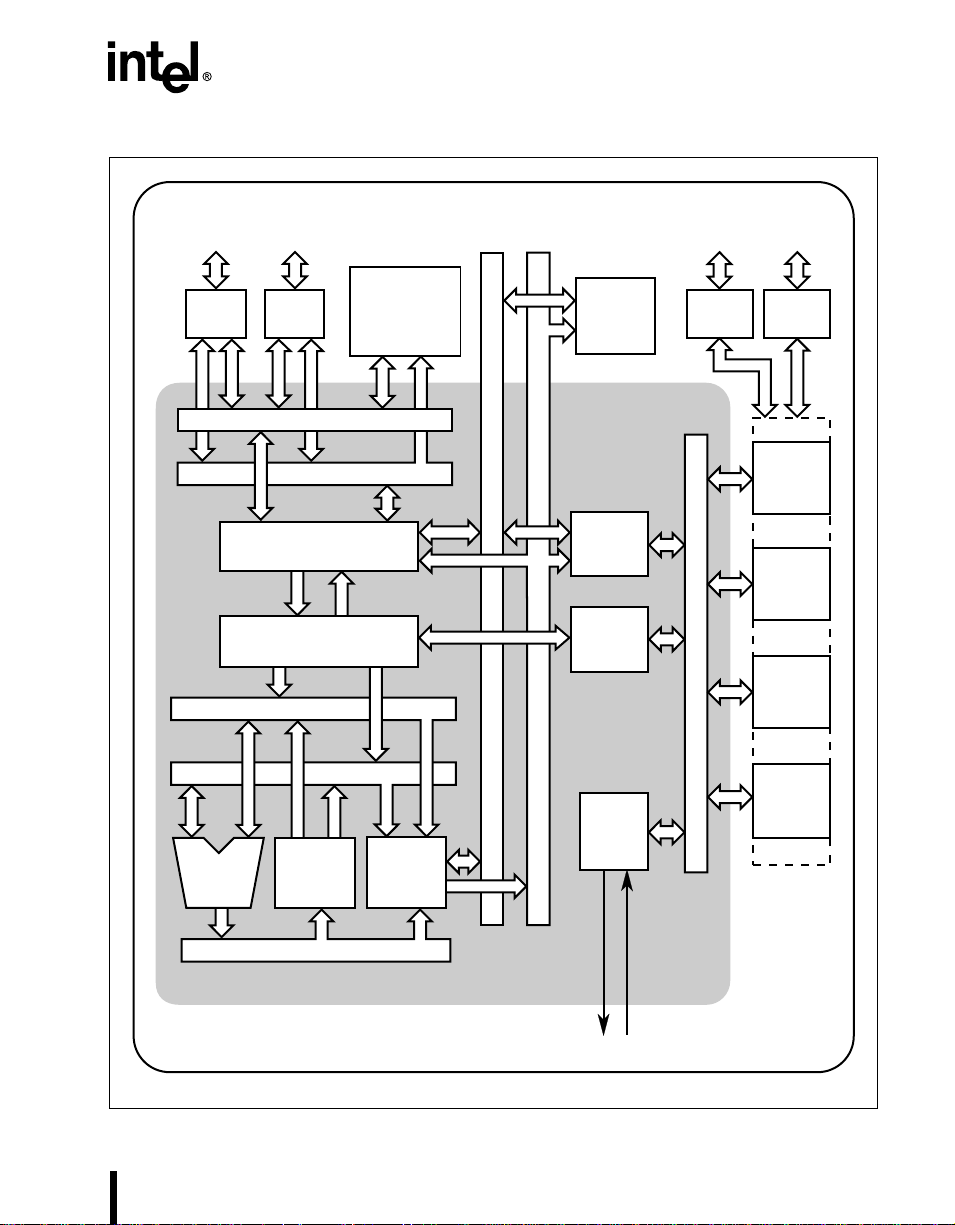
8XC251SA/SB/SP/SQ HIGH-PERFORMANCE CHMOS MICROCONTROLLER
System Bus and I/O Ports
P0.7:0
Port 0
Drivers
Code Bus (16)
SRC1 (8)
SRC2 (8)
ALU
P2.7:0
Port 2
Drivers
Memory Data (16)
Memory Address (16)
Bus Interface
Instruction Sequencer
Register
File
Code
OTPROM/ROM
8 Kbytes
or
16 Kbytes
Code Address (24)
Data
Memory
Interface
Data Address (24)
Data Bus (8)
Data RAM
512 Bytes
or
1024 Bytes
Peripheral
Interface
Interrupt
Handler
Clock
&
Reset
I/O Ports and
Peripheral Signals
P1.7:0
Port 1
Drivers
IB Bus (8)
P3.7:0
Port 3
Drivers
Watchdog
Timer
Timer/
Counters
PCA
Serial I/O
Peripherals
DST (16)
®
MCS
251 Microcontroller Core
Clock & Reset
8XC251SA/SB/SP/SQ Microcontroller
A4214-01
Figure 1. 8XC251SA/SB/SP/SQ Block Diagram
PRELIMINARY 3
Page 4
8XC251SA/SB/SP/SQ HIGH-PERFORMANCE CHMOS MICROCONTROLLER
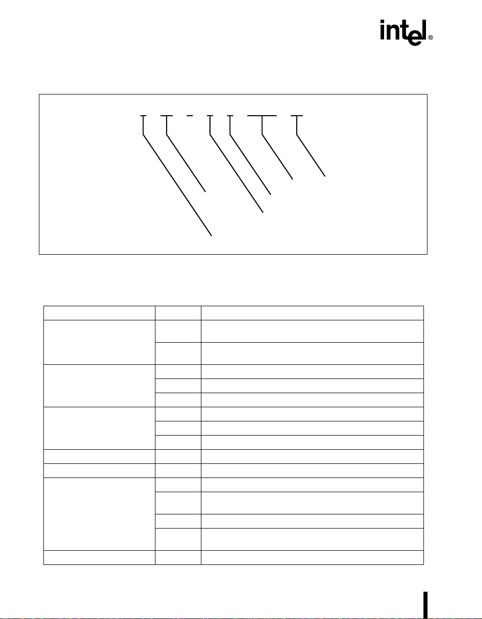
1.0 NOMENCLATURE
XXXXX XXXX8XXX
Program-memory Options
Packaging Options
Temperature and Burn-in Options
Figure 2. The 8XC251SA/SB/SP/SQ Family Nomenclature
Table 1. Descriptio n of Pro duc t Nomenc lat ure
Parame ter Options Descript ion
Temperature and Burn-in
Options
Packaging Options N 44-pin Plastic Leaded Chip Carrier (PLCC)
Program Memory Options 0 Without ROM/OTPROM/EPROM
Process Information C CHMOS
Product Family 251 8-bit control architecture
Device Memory Options SA 1-Kbyte RAM/8-Kbyte ROM/OTPROM/EPROM
Device Speed 16 External clock frequency
no mark Commercial operating temperature range (0°C to 70°C) with
T Express operat ing tempe rat ure range (-40 °C to 85°C) with
P 40-pin Plastic Dual In-line Package (PDIP)
C 40-pin Ceramic Dual In-lin e Package (Cera mic DIP)
3ROM
7 User programmable OTPROM/EPROM
SB 1-Kbyte RAM/16-Kb yt e ROM/OT PROM /EPROM or withou t
SP 512-byte RAM/8-Kbyte ROM/OTPROM/EPROM
SQ 512-byte RAM/16-Kbyte ROM/OTPROM/EPROM or without
Process Information
Intel stan dard bu rn-in.
Intel stan dard bu rn-in.
ROM/OTPROM/EPROM
ROM/OTPROM/EPROM
Product Family
Device Speed
A2815-01
4 PRELIMINARY
Page 5
8XC251SA/SB/SP/SQ HIGH-PERFORMANCE CHMOS MICROCONTROLLER
Table 2 lists the proliferation op tions. See Figure 2 for the 8XC2 51 SA/S B/SP/ SQ fam ily nome ncla tu re.
.
Table 3 lists the 8XC251SA/SB/SP/SQ packages.
N 44 ld. PLCC 0°C to +70°C
P 40 ld. Plastic DIP 0°C to +70°C
C 40 ld. Ceramic DIP 0°C to +70°C
TN 44 ld. PLCC -40°C to +85°C
TP 40 ld. Plastic DIP -40°C to +85°C
Table 2. Proliferation Options
8XC251SA/SB /SP/ SQ
(0 – 16 MHz; 5 V ±10%)
80C251SB16 C PU-on ly
80C251SQ1 6 CPU-only
83C251 SA1 6 ROM
83C251 SB1 6 ROM
83C251 SP1 6 ROM
83C251 SQ1 6 ROM
87C251SA16 OTPROM/EPROM
87C251SB16 OTPROM/EPROM
87C251SP16 OTPROM/EPROM
87C251SQ16 OTPROM/EPROM
T able 3. Package Information
Pkg. Definitio n Tempera ture
PRELIMINARY 5
Page 6
8XC251SA/SB/SP/SQ HIGH-PERFORMANCE CHMOS MICROCONTROLLER
AD4 / P0.4
AD5 / P0.5
AD6 / P0.6
AD7 / P0.7
EA# / V
PP
V
SS2
ALE / PROG#
PSEN#
A15 / P2.7
A14 / P2.6
A13 / P2.5
P1.4 / CEX1
P1.3 / CEX0
P1.2 / ECI
P1.1 / T2EX
P1.0 / T2
V
SS1
V
CC
AD0 / P0.0
AD1 / P0.1
AD2 / P0.2
AD3 / P0.3
A4205-02
P1.5 / CEX2
P1.6 / CEX3 / WAIT#
P1.7 / CEX4 / A17 / WCLK
RST
P3.0 / RXD
V
CC2
P3.1 / TXD
P3.2 / INT0#
P3.3 / INT1#
P3.4 / T0
P3.5 / T1
39
38
37
36
35
34
33
32
31
30
29
8XC251SA
8XC251SB
8XC251SP
8XC251SQ
View of component as
mounted on PC board
7
8
9
10
11
12
13
14
15
16
17
P3.6 / WR#
P3.7 / RD# / A16
XTAL2
XTAL1
V
SS
V
SS2
A8 / P2.0
A9 / P2.1
A10 / P2.2
A11 / P2.3
A12 / P2.4
18
19
20
21
22
23
24
25
26
27
28
65432
1
44
43
42
41
40
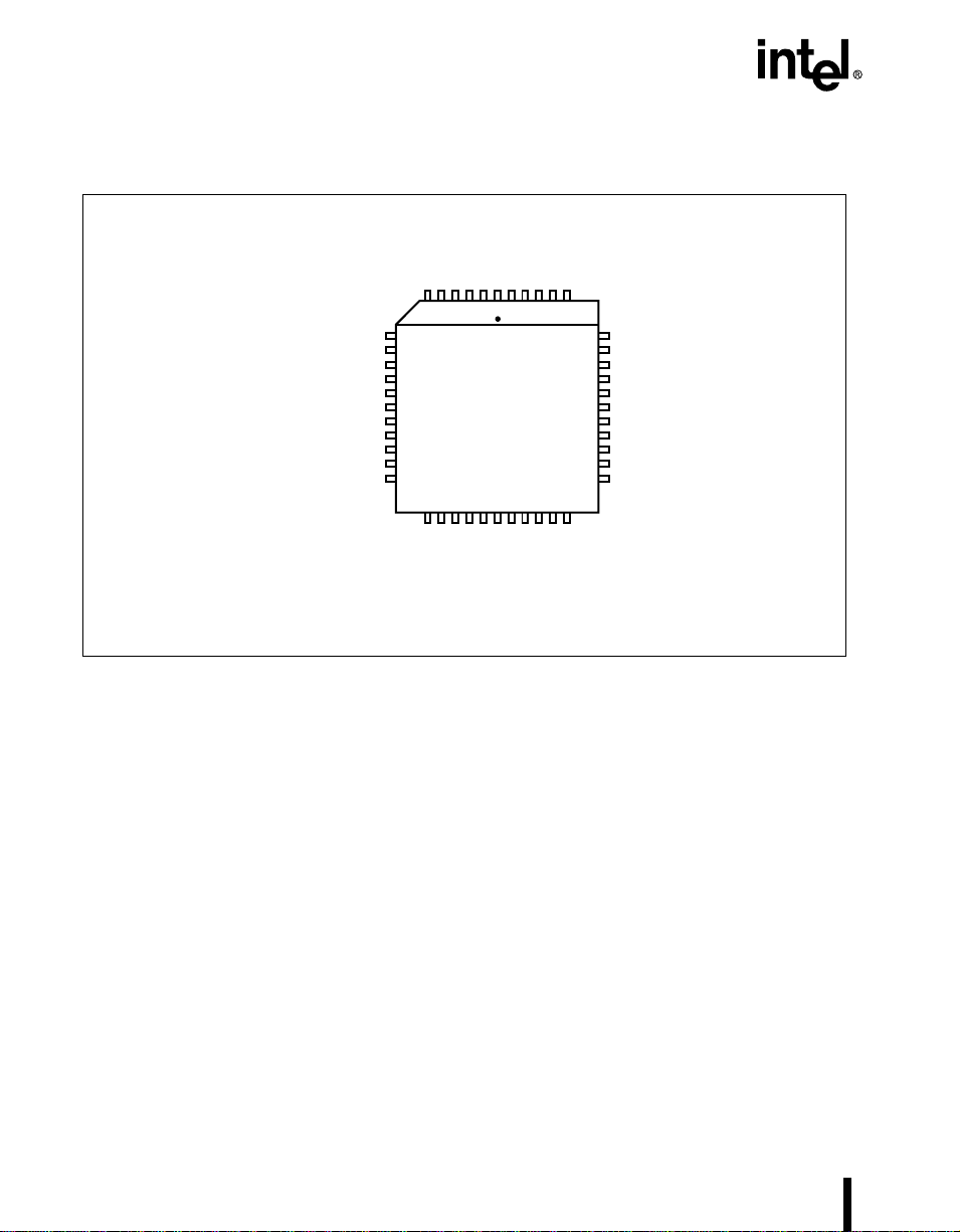
2.0 PINOUT
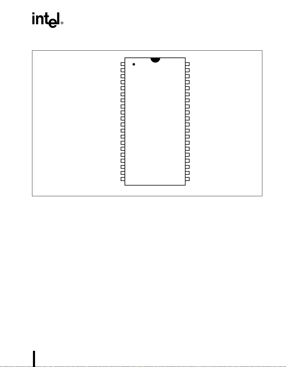
Figure 3. 8XC251SA/SB/SP /SQ 44-p in PLCC Package
6 PRELIMINARY
Page 7
8XC251SA/SB/SP/SQ HIGH-PERFORMANCE CHMOS MICROCONTROLLER
P1.0 / T2
P1.1 / T2EX
P1.2 / ECI
P1.3 / CEX0
P1.4 / CEX1
P1.5 / CEX2
P1.6 / CEX3 / WAIT#
P1.7 / CEX4 / A17 / WCLK
RST
P3.0 / RXD
P3.1 / TXD
P3.2 / INT0#
P3.3 / INT1#
P3.4 / T0
P3.5 / T1
P3.6 / WR#
P3.7 / RD# / A16
XTAL2
XTAL1
V
1
2
3
4
5
8XC251SA
6
8XC251SB
7
8XC251SP
8
8XC251SQ
9
10
11
12
13
14
15
16
17
18
19
20
SS
View of
component
as mounted
on PC board
40
39
38
37
36
35
34
33
32
31
30
29
28
27
26
25
24
23
22
21
V
CC
AD0 / P0.0
AD1 / P0.1
AD2 / P0.2
AD3 / P0.3
AD4 / P0.4
AD5 / P0.5
AD6 / P0.6
AD7 / P0.7
V
EA# /
PP
ALE / PROG#
PSEN#
A15 / P2.7
A14 / P2.6
A13 / P2.5
A12 / P2.4
A11 / P2.3
A10 / P2.2
A9 / P2.1
A8 / P2.0
Figure 4. 8XC251SA/ SB/SP /SQ 40-pin PDIP an d Ceram ic DIP Package s
A4206-03
PRELIMINARY 7
Page 8
8XC251SA/SB/SP/SQ HIGH-PERFORMANCE CHMOS MICROCONTROLLER
Table 4. 8XC251SA/SB/S P/SQ Pin Ass ignme nt
PLCC DIP Name PLCC DIP Name
1
2 1 P1.0/T2 24 21 A8/P2.0
3 2 P1.1/T2EX 25 22 A9/P2.1
4 3 P1.2/ECI 26 23 A10/P2.2
5 4 P1.3/CEX0 27 24 A11/P2.3
6 5 P1.4/CEX1 28 25 A12/P2.4
7 6 P1.5/CEX2 29 26 A13/P2.5
8 7 P1.6/CEX3/WAIT# 30 27 A14/P2.6
9 8 P1.7/CEX4/A17/WCLK 31 28 A15/P2.7
10 9 RST 32 29 PSEN#
11 10 P3.0/RXD 33 30 ALE/PROG#
12
13 11 P3.1/TXD 35 31 EA#/V
14 12 P3.2/INT0# 36 32 AD7/P0.7
15 13 P3.3/INT1# 37 33 AD6/P0.6
16 14 P3.4/T0 38 34 AD5/P0.5
17 15 P3.5/T1 39 35 AD4/P0.4
18 16 P3.6/WR# 40 36 AD3/P0.3
19 17 P3.7/RD#/A16 41 37 AD2/P0.2
20 18 XTAL2 42 38 AD1/P0.1
21 19 XTAL1 43 39 AD0/P0.0
22 20 V
V
SS1
V
CC2
SS
23 V
34 V
44 40 V
SS2
SS2
CC
PP
8 PRELIMINARY
Page 9
8XC251SA/SB/SP/SQ HIGH-PERFORMANCE CHMOS MICROCONTROLLER
Table 5. 8XC251SA/SB/SP/SQ PLCC/DIP Pin Assignments Arranged by Functional Category
Address & Data Input/Output
Name PLCC DIP Name PLCC DIP
AD0/ P 0.0 43 39 P1.0/T2 2 1
AD1/ P 0.1 42 38 P1.1/T2 EX 3 2
AD2/ P 0.2 41 37 P1.2/ECI 4 3
AD3/ P 0.3 40 36 P1.3/CEX0 5 4
AD4/ P 0.4 39 35 P1.4/CEX1 6 5
AD5/ P 0.5 38 34 P1.5/CEX2 7 6
AD6/P0.6 37 33 P1.6/CE X3/ WAIT# 8 7
AD7/P0.7 36 32 P1.7/CEX4/ A17/WC LK 9 8
A8/P2.0 24 21 P3.0/RXD 11 10
A9/P2.1 25 22 P3. 1/T XD 13 11
A10/P2.2 2623 P3.4/T0 1614
A11/P2.3 27 24 P3.5/T1 17 15
A12/P2.4 28 25
A13/P2.5 29 26 Power & Ground
A14/P2.6 30 27 Name PLCC DIP
A15/P2.7 31 28 V
P3.7/RD#/A16 19 17 V
P1.7/CEX4/A17/WCLK 9 8 V
CC
CC2
SS
V
SS1
V
SS2
Processor Control EA#/VPP 35 31
Name PLCC DIP
P3.2/INT0# 14 12 Bus Control & Status
P3.3/INT1# 15 13 Name PLCC DIP
EA#/V
PP
35 31 P3.6/WR# 18 16
RST 10 9 P3.7/RD#/A16 19 17
XTAL1 21 18 ALE/PROG# 33 30
XTAL2 20 19 PSEN# 32 29
44 40
12
22 20
1
23, 34
PRELIMINARY 9
Page 10
8XC251SA/SB/SP/SQ HIGH-PERFORMANCE CHMOS MICROCONTROLLER
3.0 SIGNALS
Table 6. Signal Descriptions
Signal
Name
Type Description
A17 O 18th Address Bit (A17). Output to memory as 18th external address
bit (A17) in extended bus applications, depending on the values of bits
RD0 and RD1 in configuration byte UCONFIG0 (see Chapte r 4,
“Device Configuration,” of the 8XC251SA/SB/SP/SQ Embedded
Microcontroller User ’s Man ual). See also RD# and PSEN# .
A16 O Address Line 16. See RD#. RD#
†
A15:8
AD7:0
O Address Lines. Upper address lines for the external bus. P2.7:0
†
I/O Address/Data Lines. Multiplexed lower address lines and data lines
for external memory.
ALE O Address Latch Enable. ALE signals the start of an external bus cycle
and indicates that valid address information is available on lines A15:8
and AD7:0. An externa l latch can use ALE to demulti pl ex the addre ss
from the address/data bus.
CEX4:0 I/O Programmable Counter Array (PCA) Input/Output Pins. These are
EA# I External Access. Directs program memory accesses to on-chip or off-
input signals for the PCA capture mode and output signals for the PCA
compare mo de and PCA PWM mo de .
chip code memory. For EA# = 0, all program memory accesses are offchip. For EA# = 1, an access is to on-chip ROM/OTPROM/EPROM if
the address is within the range of the on-chip
ROM/OTPROM/EP ROM; otherwise the acce ss is off-chip. The value
of EA# is latched at reset. For devices without on-chip
ROM/OTPROM/EPROM, EA# must be strapped to ground.
ECI I PCA External Clock Input. External clock input to the 16-bit PCA
INT1:0# I External Interrupts 0 and 1. These inp uts se t bits IE1: 0 in the TCON
timer.
register. If bits IT1:0 in the TCON register are set, bits IE1:0 are set by
a falling edge on INT1 #/INT0#. If bits INT1:0 are clear, bits IE1:0 are
set by a low level on INT1:0#.
PROG# I Programming Pulse. The program min g puls e is app li ed to thi s pin fo r
programming the on-chip OTPROM.
P0.7:0 I/O Port 0. This is an 8-bit, open-d rain, bi directio na l I/O port . AD7:0
P1.0
P1.1
P1.2
P1.7:3
I/O Port 1. This is an 8-bit, bidirection al I/O port with in tern a l pullu ps. T2
P2.7:0 I/O Port 2. This is an 8-bit, bidirection al I/O port with in tern a l pullu ps. A15: 8
†
The descripti ons of A15 :8 /P2 .7: 0 and AD7:0 /P0.7:0 are for the nonpa ge-mo de chip conf igu ra tio n (com patible with 44-pin PLCC and 40-pin DIP MCS 51 microcontro llers). If the chip is configured for pagemode operation, port 0 carries the lower address bits (A7:0), and port 2 carries the upper address bits
(A15:8) and the data (D7:0).
Alternate
Function
P1.7/CEX4/
WCLK
P0.7:0
PROG#
P1.6 :3
P1.7 /A17/
WAIT#
V
PP
P1.2
P3.3:2
ALE
T2EX
ECI
CEX3: 0
CEX4/ A17 /
WAIT#/
WCLK
10 PRELIMINARY
Page 11
8XC251SA/SB/SP/SQ HIGH-PERFORMANCE CHMOS MICROCONTROLLER
Table 6. Signal Descriptions (Contin ued )
Signal
Name
P3.0
P3.1
P3.3:2
P3.5:4
P3.6
Type Description
I/O Port 3. This is an 8-bit, bid ire ctio na l I/O port with intern al pull ups. RXD
P3.7
PSEN# O Program Store Enab le. Read signal output. This output is asserted
RD# O Read or 17th Address Bit (A16). Read signal ou tput to exte rna l data
for a memory address range that depends on bits RD0 and RD1 in
configuratio n byte UCONFIG0 (see RD# and Chapter 4, “Device Configuration,” in the 8XC251SA/SB/SP/SQ Embedded Microcontroller
User’s Manual) .
memory or 17th external address bit (A16), depending on the values of
bits RD0 and RD1 in configuration byte UCONFIG0. (See PSEN# and
Chapter 4, “Device Configuration,” in the 8XC251SA/SB/SP/SQ
Embedded Microcontroller User’s Manual).
RST I Reset. Reset input to the chip. Holding this pin high for 64 oscillator
periods while the oscillator is running resets the device. The port pins
are driven to their reset condit ions when a volta ge great er tha n V
applied, whether or not the oscillator is running. This pin has an internal pulldown resistor, which allows the device to be reset by connecting a capacitor between this pin and V
Asserting RST when the chip is in idle mode or powerdown mode
returns the chip to normal operation.
CC
.
IH1
RXD I/O Receive Serial Data. RXD sends and receives data in serial I/O mode
0 and receives data in serial I/O mode s 1, 2, and 3.
T1:0 I Timer 1:0 External Clock Inputs. When timer 1:0 operates as a
counter, a falling edge on the T1:0 pin increments the count.
T2 I/O Timer 2 Clock Input/Output. For the timer 2 capture mode, this signal
is the external clock input. For the clock-out mode, it is the timer 2
clock output.
T2EX I Tim e r 2 External Input. In timer 2 ca ptu re mo de , a fallin g ed ge ini-
TXD O Transmit Serial Data. TXD outputs the shift clock in serial I/O mode 0
V
CC
V
CC2
†
The descriptions of A15:8/P2.7:0 and AD7:0/P0.7:0 are for the nonpage-mode chip configuration (com-
tiates a capture of the timer 2 registers. In auto-reload mode, a falling
edge causes the timer 2 registers to be reloaded. In the up-down
counter mode, this signal determ ines th e count dire ctio n: 1 = up, 0 =
down.
and tran smit s se ria l da ta in seria l I/O mo de s 1, 2, and 3.
PWR Supply Voltage. Connect this pin to the +5V supply voltage. —
PWR Secondary Supply Voltage 2. This supply voltage connection is pro-
vided to reduce power supply noise. Connection of this pin to the +5V
supply voltage is recommended. However, when using the 8XC251SB
as a pin-for-pin replacement for the 8XC51FX, V
nected withou t loss of compati bility. (Not available on DIP)
can be uncon-
SS2
patible with 44-pin PLCC and 40-pin DIP MCS 51 microcontrollers). If the chip is configured for pagemode operation, po rt 0 carries the lower addre ss bit s (A7: 0), and port 2 carries the upper address b its
(A15:8) and the data (D7:0).
is
Alternate
Functio n
TXD
INT1:0#
T1:0
WR#
RD#/A16
—
P3.7/A16
—
P3.0
P3.5:4
P1.0
P1.1
P3.1
—
PRELIMINARY 11
Page 12

8XC251SA/SB/SP/SQ HIGH-PERFORMANCE CHMOS MICROCONTROLLER
Table 6. Signal Descriptions (Continued)
Signal
Name
V
PP
V
SS
V
SS1
V
SS2
Type Description
I Programmi ng Sup ply Voltage. The programming supply voltage is
applied to this pin for programming the on-chip OTPROM/EPROM.
GND Circuit Ground. Connect this pin to ground. —
GND Secondary Ground. This ground is provided to reduce ground bounce
and improve power supply bypassing. Connection of this pin to ground
is recommended. However, when using the 8XC251SA/SB/SP/SQ as
a pin-for-pin repla ce men t for the 8XC51 BH, V
without loss of compatibility. (Not available on DIP)
GND Secondary Ground 2. This ground is provided to reduce gro und
bounce and improve power supply bypassing. Connection of this pin to
ground is recomme nded . Howe ve r, when using the 8XC251 SB as a
pin-for-p in replacement for the 8XC5 1FX , V
without loss of compatibility. (Not available on DIP)
can be unconnected
SS1
can be unconnected
SS2
WAIT# I Real-time Wait State Input. The real-time WAIT# input is enabled by
writing a logical ‘1’ to the WCON.0 (RTWE) bit at S:A7H. During bus
cycles, the external memory system can signal ‘system ready’ to the
microcontroller in real time by controlling the WAIT# input signal on the
por t 1.6 input.
WCLK O Wait Clock Output. The real-time WCLK output is driven at port 1.7
(WCLK) by writing a logical ‘1’ to the WCON.1 (RTWCE) bit at S:A7H.
When enabled, the WCLK output produces a square wave signal with
a period of one-half the oscillator frequency.
WR# O Write. Write signal output to external memory. P3.6
XTAL1 I Input to the On-chip, Inverting, Oscillator Amplifier. To use the
internal oscillator, a crystal/resonator circuit is connected to this pin. If
an external oscillator is used, its output is connected to this pin. XTAL1
is the clock source for internal timing.
XTAL2 O Output of the On-chi p, Inv ertin g, Oscillator Amp lifi er. To use the
internal oscillator, a crystal/resonator circuit is connected to this pin. If
an external oscillator is used, leave XTAL2 unconnected.
†
The descripti ons of A15 :8 /P2 .7: 0 and AD7:0 /P0.7:0 are for the nonpa ge-mo de chip conf igu ra tio n (com patible with 44-pin PLCC and 40-pin DIP MCS 51 microcontro llers). If the chip is configured for pagemode operation, port 0 carries the lower address bits (A7:0), and port 2 carries the upper address bits
(A15:8) and the data (D7:0).
Alternate
Function
EA#
—
—
P1.6/CEX3
P1.7/CEX4/
A17
—
—
12 PRELIMINARY
Page 13

8XC251SA/SB/SP/SQ HIGH-PERFORMANCE CHMOS MICROCONTROLLER
Table 7. Memory Signal Selections (RD1:0)
RD1:0
0 0 A17 A16 Asserted for
0 1 P1.7/CEX4/
1 0 P1.7/CEX4/
1 1 P1.7/CEX4/
P1.7/CEX/
A17/WCLK
WCLK
WCLK
WCLK
P3.7/RD#/A16 PSEN# WR# Features
all addre sses
A16 Asserted for
P3.7 only Asserted for
RD# asserted
for addresses
≤ 7F:FFFFH
all addre sses
all addre sses
Asserted for
≥ 80:0 000H
Asserted for writes to
all memory locatio ns
Asserted for writes to
all memory locatio ns
Asserted for writes to
all memory locatio ns
Asserted only for
writes to MCS 51
microcontroller data
memo ry locations.
256-Kbyte external
memory
128-Kbyte external
memory
64-Kbyte external
memory. One
additional port pin.
64-Kbyte external
memory. Compatible
with MCS 51 microcontrollers.
PRELIMINARY 13
Page 14

8XC251SA/SB/SP/SQ HIGH-PERFORMANCE CHMOS MICROCONTROLLER
4.0 ADDRESS MAP
Table 8. 8XC251SA/SB/SP/SQ Address Map
Internal
Address)
FF:FFFFH
FF:400 0H
FF:3FF F H
FF:000 0H
FE:FFFF H
FE:000 0H
External Memory except the top eight bytes (FF:FFF8H–FF:FFFFH) which are
reserved for the configuration array.
External memory or on-chip nonvolatile memory (8Kbytes FF:0000H - FF:1FFFH,
16Kbytes FF:0000H - FF:3FFFH).
External Memory 3
Description Notes
1, 3, 10
3, 4, 5
FD:FFFFH
02:0000H
01:FFFFH
01:0000H
00:FFFFH
00:E000H
00:DFFFH
00:0420H
00:041FH
00:0080H
00:007FH
00:0020H
00:001FH
00:0000H
NOTES:
1. 18 addres s lines are bo nded out (A15 :0 , A16:0, or A17:0 selecte d dur ing chip conf igu ra tio n).
2. The special functi on registe rs (SF Rs) and the regi ster file have se para te intern al address space s.
3. Data in this area is accessible by indirect addressing only .
4. Devices reset into internal or external starting locations depending on the state of EA# and configuration byte information See EA#. See also UCONFIG1:0 bit definitions in the 8XC251SA/SB /SP/ SQ
Embedded Microcon tro ller User ’s Man ual.
5. The 16-Kbyte ROM/OTPROM/EPROM devices allow internal locations FF:2000H–FF:3FFFH to map
into region 00:. In this case, if EA# = 1, a data read to 00:E000H–00:FFFFH is redirected to internal
ROM/OTPROM /EPROM (see bit 1 in UCONFIG0). This is not available for 8-Kbyte
ROM/OTPROM/EPROM devices.
6. This reserved area returns indet ermin at e values.
7. Data is accessible by direct and indirect addressing.
8. Data is accessible by direct, indirect, and bit addressing.
9. Data is accessible by direct, indirect, and register addressing.
10. Eight addresse s at the top of all external memor y maps are reser ved for current and future device
configuration byte information.
Reserved 6
External Memory 3
External memory or with configuration bit EMAP# = 0, addresses in this range
access on-chip code memory in region FF: (16 Kbyte devices only).
External Memory 7
On-chip RAM (512 byte s 00:0020 H - 00:021FH, 102 4 bytes 00:00 20H -
00:041FH)
On-chip RAM 8
Storag e for R0– R7 of Reg ister File 2, 9
5, 7
7
14 PRELIMINARY
Page 15

8XC251SA/SB/SP/SQ HIGH-PERFORMANCE CHMOS MICROCONTROLLER
5.0 ELECTRICAL CHARACTERISTICS
ABSOLUTE MAXIMUM RATINGS
Storage Temperature ................................... -65°C to +150°C
Voltage on EA#/V
Voltage on Any other Pin to V
per I/O Pin................................................................. 15 mA
I
OL
Power Dissipation .......................................................... 1.5 W
OPERATING CONDITIONS
TA (Ambient Temperature Under Bias):
Commercial ................................................. 0°C to +70°C
Express ....................................................-40°C to +85°C
V
(Digital Supply Voltage) .............................. 4.5 V to 5.5 V
CC
..................................................................................... 0 V
V
SS
Pin to VSS......................... 0 V to +13.0 V
PP
..................... -0.5 V to +6.5 V
SS
†
NOTE
Maximum power dissipation is
based on package heat-transfer
limitations, not device power
consumption.
NOTICE: This document contains preliminary
information on new products in production. The
specifications are subject to change without notice.
Verify with your local Intel sale s office that you
have the latest datasheet before finalizing a
design.
†
WARNING: Stressing the device beyond the
“Absolute Maximum Ratings” may cause permanent damage. These are stress ratings only. Operation beyond the “Operating Conditions” is not
recommended and extended exposure beyond the
“Operating Conditions” may affect device
reliability.
PRELIMINARY 15
Page 16

8XC251SA/SB/SP/SQ HIGH-PERFORMANCE CHMOS MICROCONTROLLER
5.1 D.C. Characteristics
Parameter values apply to all devices unless otherwise indicated.
Table 9. DC Charac teris tics at V
= 4.5 – 5.5 V
CC
Symbol Param ete r Mi n Typical Max Units Test Conditions
V
IL
V
IL1
V
IH
V
IH1
V
OL
Input Low Voltage
(except EA#)
Input Low Voltage
(EA#)
Input High Voltage
(except XTAL1, RST)
Input High Voltage
(XTAL1, RST)
Output Low Voltage
(Port 1, 2, 3)
-0.5 0.2VCC – 0.1 V
0 0.2VCC – 0.3 V
0.2VCC + 0.9 VCC + 0.5 V
0.7VCC V
+ 0.5 V
CC
0.3
0.45
1.0
VIOL = 100 µA
= 1.6 mA
I
OL
= 3.5 mA
I
OL
(Note 1, Note 2)
V
OL1
Output Low Voltage
(Port 0, ALE, PSEN#)
0.3
0.45
1.0
VIOL = 200 µA
= 3.2 mA
I
OL
= 7.0 mA
I
OL
(Note 1, Note 2)
V
OH
Output High Voltage
(Port 1, 2, 3, ALE,
PSEN#)
V
– 0.3
CC
– 0.7
V
CC
– 1.5
V
CC
VI
= -10 µA
OH
= -30 µA
I
OH
= -60 µA
I
OH
(Note 3)
NOTES:
1. Under steady-state (non-transient) conditions, I
Maximum I
Maximum I
per port pin: 10 mA
OL
per 8-bit port:
OL
port 0 26 mA
must be externally limited as follows:
OL
ports 1–3 15 mA
Maximum Total I
all output pins 71 mA
If I
exceeds the test conditions, VOL may exceed the related specificati on. Pins are not guarante ed
OL
to sink current greater than the listed test conditions.
for
OL
2. Capacitive loading on ports 0 and 2 may cause spurious noise pulses above 0.4 V on the low-level
outputs of ALE and ports 1, 2, and 3. The noise is due to external bus capacitance discharging into
the port 0 and port 2 pins when these pins change fro m high to low. In applications where capa citive
loading exceeds 100 pF, the noise pulses on these signals may exceed 0.8 V. It may be desirable to
qualify ALE or other signals with a Schmitt trigger or CMOS-level input logic.
3. Capacitive loading on ports 0 and 2 causes the V
tion when the address lines are stabilizing.
4. Typical values are obtained using V
= 5.0 , TA = 25°C and are not guaranteed.
CC
on ALE and PSEN# to drop below the specifica-
OH
16 PRELIMINARY
Page 17

8XC251SA/SB/SP/SQ HIGH-PERFORMANCE CHMOS MICROCONTROLLER
Table 9. DC Characteristics at V
= 4.5 – 5.5 V (Continued)
CC
Symbol Parameter Min Typical Max Units Test Conditions
V
OH1
V
OH2
Output High Voltage
(Port 0 in External
Address)
Output High Voltage
(Port 2 in External
Address during Page
Mode)
I
IL
I
LI
I
TL
R
RST
C
IO
I
PD
Logical 0 Input Current (Port 1, 2, 3)
Input Leakage Current (Port 0)
Logical 1-to-0 Transition Current (Port 1,
2, 3)
RST Pulldown Resistor
Pin Capacitance 10
Powerdown Current 10
VCC – 0.3
– 0.7
V
CC
– 1.5
V
CC
VCC – 0.3
– 0.7
V
CC
– 1.5
V
CC
-50 µA VIN = 0.45 V
+/-10 µA 0.45 < VIN < V
-650 µA VIN = 2.0 V
40 225 kΩ
(Note 4)
20 µA
VI
OH
I
OH
I
OH
VI
OH
I
OH
I
OH
pF F
OSC
= 25 °C
T
A
= -200 µA
= -3.2 mA
= -7.0 mA
= -200 µA
= -3.2 mA
= -7.0 mA
= 16 MHz
(Note 4)
I
DL
Idle Mode Current 12
15 mA F
= 16 MHz
OSC
(Note 4)
I
CC
Operating Current 45
80 mA F
= 16 MHz
OSC
(Note 4)
NOTES:
1. Under steady-state (non-transient) conditions, I
Maximum I
Maximum I
per port pin: 10 mA
OL
per 8-bit port:
OL
port 0 26 mA
must be externally limited as follows:
OL
ports 1–3 15 mA
Maximum Total I
all outp ut pins 71 mA
exceeds the test conditions, VOL may exceed the related specification. Pins are not guaranteed
If I
OL
to sink current great er tha n the listed test conditio ns.
for
OL
2. Capacitive loading on ports 0 and 2 may cause spurious noi se pulse s above 0.4 V on the low-leve l
outputs of ALE and ports 1, 2, and 3. The noise is due to external bus capa cita nce di scharg ing into
the port 0 and port 2 pins when these pins change from high to low. In applications where capacitive
loading exceeds 100 pF, th e noise pu lses on these signa ls may exceed 0.8 V. It may be desirable to
qualify ALE or other signals with a Schmitt trigger or CMOS-level input logic.
3. Capacitive loading on ports 0 and 2 causes the V
tion when the address lines are stabilizing.
4. Typical values are obtained using V
= 5.0, TA = 25°C and are not guaranteed.
CC
on ALE and PSEN# to drop below the specifica -
OH
CC
PRELIMINARY 17
Page 18

8XC251SA/SB/SP/SQ HIGH-PERFORMANCE CHMOS MICROCONTROLLER
V
CC
I
V
CC
P0
PD
V
CC
RST
8XC251SA
8XC251SB
8XC251SP
8XC251SQ
(NC)
XTAL2
XTAL1
V
SS
All other 8XC251SA/SB/SP/SQ pins are unconnected.
Figure 5. IPD Test Condition, Powerdown Mode, VCC = 2.0 – 5.5V
70
60
50
40
(mA)
30
CC
I
max Active mode (mA)
EA#
A4208-01
typ Active mode (mA)
20
10
max Idle mode (mA)
0
21 345678910 16
typ Idle mode (mA)
11 12 13 14 15
Frequency at XTAL (MHz)
A4400-01
Figure 6. I
vs. Frequency (Mhz)
CC
18 PRELIMINARY
Page 19

8XC251SA/SB/SP/SQ HIGH-PERFORMANCE CHMOS MICROCONTROLLER
5.2 Definitio n of AC Symbols
Table 10. AC Timing Symbol Definitions
Signals Conditions
A Address H High
D Data In L Low
L ALE V Valid
Q Data Out X No Longer Valid
R RD#/PSEN# Z Floating
W WR#
5.3 A.C. Characteristics
Te st Condi tions: Capacitive load on all pins = 50 pF.
Table 11 lists AC timing parameters for the
8XC251SA/S B/SP/SQ with no wait sta tes. Externa l
wait states can be added by extending
PSEN#/RD#/ WR# and/or by extendin g ALE. In the
table, Notes 3 and 5 mark parameters affected by an
ALE wait state, and Notes 4 and 5 mark parameters
affected by a PSEN#/RD#/WR# wait state.
Figures 8–10 sho w the bus cycles with the timing
parame ters.
T able 11. AC Characteristics
Symbol Parameter
F
OSC
T
OSC
XTAL1 Frequency N/A N/A 0 16 MH z
1/F
OSC
@ 12 MHz
@ Max F
Min Max Min Max
N/A N/A
(1) F
osc
@ 16 MHz
T
T
T
LHLL
AVLL
LLAX
ALE Pulse Width
@ 12 MHz
@ 16 MHz
Address Valid to ALE Low
@ 12 MHz
@ 16 MHz
Address Hold after AL E Low
@ 12 MHz
@ 16 MHz
73.3
52.5
58.3
37.5
15
15 15
NOTES:
1. 16 MHz .
2. Specifications for PSEN# are identical to those for RD#.
3. In the formula , M=N um be r of wait st ate s (0 or 1) for ALE.
4. In the formula, N=Numb er of wait states (0,1 ,2, or 3) for RD#/PSEN# /W R#.
5. “Typical” specifications are un teste d and not gua rantee d .
83.3
62.5
(1+2M)
T
OSC
(1+2M)
T
OSC
osc
– 10
– 25
Variable
Units
ns
ns
(3)
ns
(3)
ns
PRELIMINARY 19
Page 20

8XC251SA/SB/SP/SQ HIGH-PERFORMANCE CHMOS MICROCONTROLLER
T able 11. AC Characteristics (Continued)
Symbol Parameter
T
(2) RD# or PSEN# Pulse Width
RLRH
@ 12 MHz
@ 16 MHz
T
WLWH
WR# Pulse Wid th
@ 12 MHz
@ 16 MHz
(2) ALE Low to RD# or PSEN# Low
T
LLRL
@ 12 MHz
@ 16 MHz
T
LHAX
ALE High to Address Hold
@ 12 MHz
@ 16 MHz
T
(2) RD#/PSEN# Low to valid Data/Instruction In
RLDV
@ 12 MHz
@ 16 MHz
(2) Data/Instruction Hold Time. Occurs after
T
RHDX
T
RLAZ
RD#/PSEN# are exerte d to V
OH
(2) RD# /PS EN# Low to Addre s s Float Typ.=0
@ Max F
Min Max Min Max
146.6
105
146.6
105
58.3
37.5 T
83.3
62.5
00 ns
(1) F
osc
T
T
(1+2M)T
106.6
65
2 Typ. = 0
(5)
T
RHDZ1
T
RHDZ2
T
RHLH1
T
RHLH2
T
WHLH
Instruction Float after RD#/P SEN# High
com mer cial @ 12 MHz an d 16 MHz
express @ 12 MHz and 16 MHz
Data Float after RD#/PSEN# High
@ 12 MHz
@ 16 MHz
RD#/PSEN# Hig h to ALE Hig h (Instruction)
@ 12 MHz
@ 16 MHz
RD#/PSEN# Hig h to ALE Hig h (Data)
@ 12 MHz
@ 16 MHz
WR# High to ALE High
@ 12 MHz
@ 16 MHz
Typ.=2
Typ.=2
(5)
18
5
10
5
156.6
115
10
10 10
156.6
115
171.6
130
2T
2T
NOTES:
1. 16 MHz.
2. Specificat ions for PSEN# are identi cal to those for RD#.
3. In the formula, M=Number of wait states (0 or 1) for ALE.
4. In the formula, N=Number of wait states (0,1,2, or 3) for RD#/PSEN#/WR#.
5. “Typical” specifications are untested and not guaranteed.
osc
2(1+N)
– 20
OSC
2(1+N)
– 20
OSC
– 25
OSC
(5)
Typ.=25
Typ.=25
(5)
- 10
osc
+ 5
osc
Variable
OSC
Units
2(1+N)
Tosc – 60
2ns
18
10
2Tosc – 10
ns
(4)
ns
(4)
ns
ns
(3)
ns
(4)
ns
ns
ns
ns
ns
20 PRELIMINARY
Page 21

8XC251SA/SB/SP/SQ HIGH-PERFORMANCE CHMOS MICROCONTROLLER
Table 11. AC Characteristics (Continued)
Symbol Parameter
T
AVDV1
Address (P0) Valid to Valid Data/Instru ct ion In
@ 12 MHz
@ Max F
Min Max Min Max
@ 16 MHz
T
AVDV2
Address (P2) Valid to Valid Data/Instru ct ion In
@ 12 MHz
@ 16 MHz
T
AVDV3
Address (P0) Valid to Valid Instruction In
@ 12 MHz
@ 16 MHz
T
(2) Address Valid to RD#/PSEN# Low
AVRL
T
AVWL1
T
AVWL2
T
WHQX
T
QVWH
T
WHAX
@ 12 MHz
@ 16 MHz
Address (P0) Valid to WR# Low
@ 12 MHz
@ 16 MHz
Address (P2) Valid to WR# Low
@ 12 MHz
@ 16 MHz
Data Hold after WR# High
@ 12 MHz
@ 16 MHz
Data Valid to WR# High
@ 12 MHz
@ 16 MHz
WR# High to Address Hold
@ 12 MHz
@ 16 MHz
121.6
80
126.6
85
146.6
105
63.3
42.5
138.6
97
156.6
115
NOTES:
1. 16 MHz .
2. Specifications for PSEN# are identical to those for RD#.
3. In the formula , M=N um be r of wait st ate s (0 or 1) for ALE.
4. In the formula, N=Numb er of wait states (0,1 ,2, or 3) for RD#/PSEN# /W R#.
5. “Typical” specifications are un teste d and not gua rantee d .
(1) F
osc
243.2
160
268.2
185
116.6
75
T
T
T
T
T
2T
osc
2(1+M)
– 45
OSC
2(1+M)
– 40
OSC
2(1+M)
– 20
OSC
– 20
OSC
2(1+N)
– 28
OSC
– 10
OSC
Variable
4(1+M/2)
T
OSC
4(1+M/2)
T
OSC
2T
OSC
– 90
– 65
– 50
Units
ns
(3)
ns
(3)
ns
ns
(3)
ns
(3)
ns
(3)
ns
ns
(4)
ns
PRELIMINARY 21
Page 22

8XC251SA/SB/SP/SQ HIGH-PERFORMANCE CHMOS MICROCONTROLLER
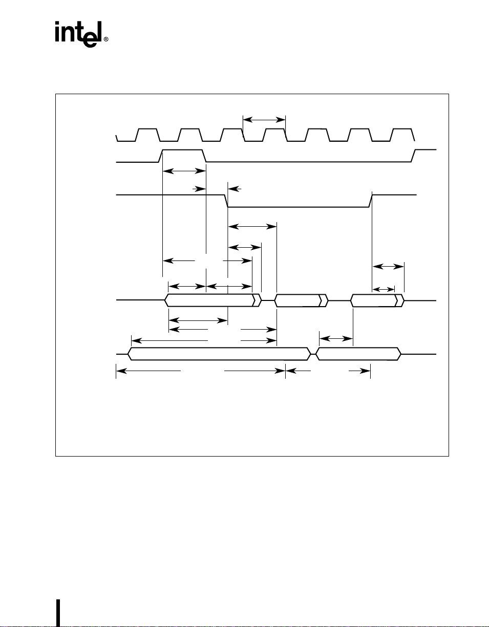
5.3.1 EXTERNAL BUS CYCLES, NONPAGE MODE
T
OSC
XTAL1
ALE
RD#/PSEN#
P0
P2/A16/A17
†
The value of this parameter depends on wait states. See the table of AC characteristics.
T
T
LLRL
LHLL
T
AVLL
†
T
†
†
T
LHAX
†
T
A7:0
†
AVRL
T
AVDV1
T
AVDV2
A15:8/A16/A17
LLAX
T
†
†
T
RLDV
RLAZ
T
RLRH
†
†
Instruction In
T
RHLH1
T
RHDZ1
T
RHDX
D7:0
Figure 7. External Bus Cycle: Code Fetch (Nonpage Mode)
A4211-03
22 PRELIMINARY
Page 23

XTAL1
8XC251SA/SB/SP/SQ HIGH-PERFORMANCE CHMOS MICROCONTROLLER
T
OSC
ALE
RD#/PSEN#
P0
P2/A16/A17
†
The value of this parameter depends on wait states. See the table of AC characteristics.
T
LHLL
T
†
AVLL
T
AVRL
T
LHAX
†
A7:0
†
T
AVDV1
T
AVDV2
†
T
LLAX
†
T
RLRH
†
T
LLRL
†
T
RLDV
T
RLAZ
†
†
A15:8/A16/A17
T
RHDZ2
T
RHDX
D7:0
Data In
T
RHLH2
Figure 8. Exte rna l Bus Cycl e: Data Read (Non page Mo de )
A4210-03
PRELIMINARY 23
Page 24

8XC251SA/SB/SP/SQ HIGH-PERFORMANCE CHMOS MICROCONTROLLER
T
OSC
XTAL1
ALE
WR#
P0
P2/A16/A17
†
The value of this parameter depends on wait states. See the table of AC characteristics.
T
LHLL
T
T
AVWL2
AVLL
T
†
T
LHAX
†
AVWL1
†
A7:0
†
T
LLAX
†
†
T
WLWH
A15:8/A16/A17
T
QVWH
T
T
WHQX
WHQX
D7:0
Data Out
T
WHAX
T
WHLH
Figure 9. External Bus Cycle: Data Write (Nonpage Mode)
A4179-01
24 PRELIMINARY
Page 25
8XC251SA/SB/SP/SQ HIGH-PERFORMANCE CHMOS MICROCONTROLLER
5.3.2 EXTERNAL BUS CYCLES, PAGE MODE
XTAL1
T
OSC
ALE
RD#/PSEN#
P2
P0/A16/A17
†
The value of this parameter depends on wait states. See the table of AC characteristics.
††
A page hit (i.e., a code fetch to the same 256-byte "page" as the previous code fetch) requires one
state (2
†††
T
); a page miss requires two states (4
OSC
During a sequence of page hits, PSEN# remains low until the end of the last page-hit cycle.
†
T
LHLL
T
T
RLAZ
†
T
LHAX
†
T
AVLL
T
Page Miss
T
LLAX
A15:8 D7:0
†
AVRL
A7:0/A16/A17
T
AVDV1
T
AVDV2
††
†
†
T
LLRL
RLDV
T
†
†
OSC
Instruction In
).
T
AVDV3
Page Hit
D7:0
Instruction In
A7:0/A16/A17
††
T
RHDZ1
T
RHDX
A4213-02
†††
Figure 10. Extern al Bus Cycle : Code Fet ch (Pa ge Mode )
PRELIMINARY 25
Page 26

8XC251SA/SB/SP/SQ HIGH-PERFORMANCE CHMOS MICROCONTROLLER
T
OSC
XTAL1
ALE
RD#/PSEN#
P2
P0/A16/A17
†
The value of this parameter depends on wait states. See the table of AC characteristics.
T
T
LLRL
LHLL
T
AVLL
†
†
T
LHAX
†
A15:8
T
AVRL
A7:0/A16/A17
T
†
T
AVDV1
T
AVDV2
†
LLAX
T
RLAZ
†
†
T
T
RLDV
RLRH
†
T
RHLH2
†
T
RHDZ2
T
RHDX
D7:0
Data In
Figure 11. External Bus Cycle: Data Read (Page Mode)
A4212-03
26 PRELIMINARY
Page 27

XTAL1
8XC251SA/SB/SP/SQ HIGH-PERFORMANCE CHMOS MICROCONTROLLER
T
OSC
ALE
WR#
P2
P0/A16/A17
†
The value of this parameter depends on wait states. See the table of AC characteristics.
T
LHLL
T
AVLL
T
AVWL2
†
T
LHAX
†
T
AVWL1
†
A15:8
†
T
LLAX
†
†
T
WLWH
A7:0/A16/A17
T
QVWH
T
T
WHQX
WHQX
D7:0
Data Out
T
WHAX
T
WHLH
Figure 12. Exte rna l Bus Cyc le: Data Write (Page Mode )
A4182-01
PRELIMINARY 27
Page 28

8XC251SA/SB/SP/SQ HIGH-PERFORMANCE CHMOS MICROCONTROLLER
5.3.3 DEFINITION OF REAL-TIME WAIT SYMBOLS
Table 12. Real-time Wait Timing Symbo l Defini tion s
Signals Conditions
A Address L Low
DData XHold
C WCL K V Setu p
Y WAIT#
W WR#
R RD# /PSE N#
5.3.4 EXT ERNAL BUS CYCLES, REAL-TIM E WAIT STATES
State 1 State 2 State 3 State 1 (next cycle)
WCLK
T
min
CLYX
T
max
ALE
RD#/PSEN#
WAIT#
T
T
RLYX
RLYX
T
max
min
RLYV
T
CLYV
CLYX
RD#/PSEN# stretched
P0
P2
A0-A7
A8-A15 stretched
A0-A7D0-D7 stretched
A8-A15
A5000-01
Figure 13. Externa l Bus Cyc le: Cod e Fetch/D ata Read (Nonp ag e Mode )
28 PRELIMINARY
Page 29

WCLK
ALE
WR#
WAIT#
8XC251SA/SB/SP/SQ HIGH-PERFORMANCE CHMOS MICROCONTROLLER
State 1 State 2 State 3 State 4
T
min
T
T
WLYX
WLYX
T
max
min
WLYV
T
CLYX
CLYV
WR# stretched
T
CLYX
max
P0
P2
WCLK
ALE
RD#/PSEN#
WAIT#
P2
P0
A0-A7
D0-D7
stretched
A8-A15 stretched
Figure 14. Extern al Bus Cycle: Data Write (Nonp ag e Mode)
State 1 State 2 State 3 State 1 (next cycle)
T
min
CLYX
T
max
CLYX
T
CLYV
RD#/PSEN# stretched
T
max
RLYX
T
min
RLYX
T
RLYV
A8-A15
A8-A15D0-D7 stretched
A0-A7 stretched
A5002-01
A0-A7
A5001-01
Figure 15. Externa l Bus Cyc le : Code Fetc h/ Data Read (Page Mode )
PRELIMINARY 29
Page 30

8XC251SA/SB/SP/SQ HIGH-PERFORMANCE CHMOS MICROCONTROLLER
State 1 State 2 State 3 State 4
WCLK
T
min
ALE
WR#
WAIT#
T
WLYX
T
WLYX
T
max
min
WLYV
T
CLYX
CLYV
WR# stretched
T
CLYX
max
P2
P0
A8-A15
D0-D7 stretched
A0-A7 stretched
A5003-01
Figure 16. External Bus Cycle: Data Write (Pag e Mode)
Table 13. Real-time Wait AC Timing
Symbol Paramete r Min Max Units
T
T
T
T
T
T
CLYV
CLYX
RLYV
RLYX
WLYV
WLYX
Wait Clock Low to Wait Set-up 0 T
Wait Hold after Wait Clock Low (2W)T
+ 5 (1+2W )T
OSC
PSEN#/RD# Low to Wait Set-up 0 T
Wait Hold after PSEN#/RD# Low (2W)T
+ 5 (1+2W)T
OSC
WR# Low to Wait Set-up 0 T
Wait Hold after WR# Low (2W)T
+ 5 (1+2W)T
OSC
– 20 ns
OSC
– 20 ns
OSC
– 20 ns
OSC
– 20 ns
OSC
– 20 ns
OSC
– 20 ns
OSC
30 PRELIMINARY
Page 31

8XC251SA/SB/SP/SQ HIGH-PERFORMANCE CHMOS MICROCONTROLLER
5.4 AC Characteristics — Serial Port, Shift Register Mode
T able 14. Serial Port Timing — Shift Register Mode
Symbol Parameter Min Max Units
T
T
T
T
T
XLXL
QVSH
XHQX
XHDX
XHDV
Serial Port Clock Cycle Time 12T
Output Data Setup to Clock Rising Edge 10T
Output Data ho ld after Clo ck Ri sing Edge 2T
OSC
– 133 ns
OSC
– 117 ns
OSC
Input Data Hold after Clock Rising Edge 0 n s
Clock Rising Edge to Input Data Valid 10T
T
XLXL
– 133 ns
OSC
ns
TXD
T
XHQX
T
RXD
(Out)
RXD
(In)
†
TI and RI are set during S1P1 of the peripheral cycle following the shift of the eighth bit.
QVXH
01 2
Valid
T
XHDV
Valid
T
XHDX
Valid Valid
3
†
T
AV
4
Valid Valid
5
6
Valid
Set TI
7
Set RI
Figure 17. Serial Port Waveform — Shift Register Mode
5.5 External Clock Dri ve
Table 15. External Clock Drive
Symbol Parameter Min Max Units
1/T
T
T
T
T
CLCL
CHCX
CLCX
CLCH
CHCL
Oscillator Frequency (F
High Time 20 ns
Low Time 20 ns
Rise Time 10 ns
Fall Time 10 ns
) 16 MHz
OSC
†
†
Valid
A2592-02
PRELIMINARY 31
Page 32

8XC251SA/SB/SP/SQ HIGH-PERFORMANCE CHMOS MICROCONTROLLER
VCC – 0.5
0.45 V
T
CLCH
0.7 VCC
T
0.2 V
CC
– 0.1
T
CHCL
CLCX
T
CLCL
Figure 18. Extern al Clock Drive Waveform s
Inputs
V
– 0.5
CC
0.45 V
AC inputs during testing are driven at V
and 0.45 V for a logic 0. Timing measurements are made at
a min of V
for a logic 1 and V
IH
0.2 V
0.2 V
CC
CC
+ 0.9
– 0.1
OL
– 0.5V for a logic 1
CC
for a logic 0.
Outputs
V
MIN
IH
V
MAX
OL
Figure 19. AC Testing Input, Output Waveforms
T
CHCX
A4119-01
A4118-01
V
V
LOAD
V
LOAD
LOAD
+ 0.1 V
Timing Reference
Points
– 0.1 V
V
V
OH
OL
– 0.1 V
+ 0.1 V
For timing purposes, a port pin is no longer floating when a
100 mV change from load voltage occurs and begins to float
when a 100 mV change from the loading V
I
= ± 20 mA.
/
with I
OL
OH
OH/VOL
level occurs
A4117-01
Figure 20 . Float Waveform s
32 PRELIMINARY
Page 33

8XC251SA/SB/SP/SQ HIGH-PERFORMANCE CHMOS MICROCONTROLLER
6.0 THERMAL CHARACTERISTIC S
All thermal impedance data is approximate for static
air conditio ns at 1 watt of power di ssipatio n. Values
change depending on operating conditions and
application requirements. The Intel
Handbook
thermal impedance test methodology.
(order n umber 240800) d escribes I ntel’s
Packaging
Table 16. The rm al Cha rac teristics
Package Type θ
44-pin PLCC 46°C/W 16°C/W
40-pin PDIP 45°C/W 16°C/W
40-pin Cera mic DIP 30.5°C/W 10°C/W
JA
7.0 NONV OL ATILE MEMORY PROGRAMMING AND V ERIFICATION
CHARACTERIS TICS
7.1 Defin iti on of Nonvo lati le M emor y Sym b ols
Table 17. Nonvolatile Mem ory Timing Symb ol Defin itio ns
Signals Conditions
A Address H High
D Data I n L Low
Q Data Out V Valid
S Supply X No Long er Valid
G PROG# Z Floating
E Enable
θ
JC
33 PRELIMINARY
Page 34

8XC251SA/SB/SP/SQ HIGH-PERFORMANCE CHMOS MICROCONTROLLER
7.2 Pro gram m in g and Verification Timing for Nonvo la til e Memo ry
Programming Cycle Verification Cycle
P1, P3
P2
T
AVGL
Data In (8 Bits)
T
DVGL
T
GHGL
T
GHDX
T
GHAX
AddressAddress (16 Bits)
T
AVQV
Data Out
PROG#
EA#/V
PP
P0
5V
12.75V
T
GLGH
T
12345
SHGL
T
EHSH
Mode (8 Bits)
T
GHSL
T
ELQV
Mode
T
EHQZ
Figure 21. Timing for Progra mm ing and Verificatio n of Nonvo lati le Mem ory
Table 18. Nonvolatile Memory Programming and Verification Characteristics at
T
= 21 – 27 °C, VCC = 5 V, and VSS = 0 V
A
Symbol Definition Min Max Units
V
I
PP
F
T
T
T
T
T
T
T
T
PP
OSC
AVGL
GHAX
DVGL
GHDX
EHSH
SHGL
GHSL
GLGH
Programming Supply Voltage 12.5 13.5 D.C. Volts
Programming Supply Current 75 mA
Oscil lator Frequency 4.0 6.0 MHz
Address Setup to PROG# Low 48T
Address Hold after PROG# 48T
Data Setup to PROG# Low 48T
Data Hold after PROG# 48T
ENABLE High to V
PP
48T
OSC
OSC
OSC
OSC
OSC
VPP Setup to PROG# Low 10 µs
VPP Hold after PROG# 10 µs
PROG# Width 90 110 µs
A4128-01
34 PRELIMINARY
Page 35

8XC251SA/SB/SP/SQ HIGH-PERFORMANCE CHMOS MICROCONTROLLER
Table 18. Nonvolatile Memory Programming and Verification Characteristics at
= 21 – 2 7 °C, VCC = 5 V, and VSS = 0 V(Continued)
T
A
T
T
T
T
AVQV
ELQV
EHQZ
GHGL
Address to Data Valid 48T
ENABLE Low to Data Valid 48T
Data Float after ENABLE 0 48T
PROG# High to PROG# Low 10 µs
8.0 ERRATA
There are no known errata for this product.
9.0 REVIS ION HIS T ORY
This (-003) revision of the 8XC251SA/SB/SP/SQ
datasheet contains information on products with
“[M] [C] '94 '95 C” as the last line of the topside
marking. This datasheet replaces earlier product
inform atio n. The foll owing chang es appe ar in the 003 datasheet:
1. Real-time wait state operation is described in
the d atasheet.
2. Memory map reserved locations are newly
defined and the Memory Map is now referred
to as the “Address Map.”
3. AC Characteristics have been updated. The
following AC parameters have changed: T
, T
, T
, T
, T
AVRL
RHDZ1
, T
, T
AVWL1
RHDZ2
T
RLRH
WLWH
LLRL
T
, T
WHLH
AVDV1
, an d T
T
QVWH
4. DC Characteristi cs have be en upd ated. The
, T
WHAX
AVDV2
.
RLDV
, T
following DC specs have changed: I
typical, I
5. An I
6. Process information is no longer contained in
max, ICC typical, and ICC max.
DL
vs. Frequency graph is included.
CC
the d atasheet.
7. The section “Progra mmi ng and Verifying Nonvolatile Memory” has been deleted. See the
8XC251SA/SB/SP/SQ Embedded Microcontroller User’s Manual. Timing and Characteristics for Programming and Verifying Nonvolatile
, T
AVWL2
PD
LLAX
, T
RHLH2
,
max, IDL
OSC
OSC
OSC
memory have been retained in this datasheet.
8. Signature Byte information has been deleted.
See the 8XC251SA/SB/SP/SQ Embedded
Microcontroller User’s Manual.
9. Sections in the datasheet are numbered.
10. New sections have been create d to provide
better organization. These include “Nomenclature,” “Pinout,” “Signals,” “Address Map,”
“Electrical Characteristics,” “Thermal Characteristics,” “Nonvolatile Memory Programming
and Verification Characteristics”, “Errat a,” and
“Revision History”
1 1. Proliferation Options and Package Options are
in the Nomenclature section.
12. Temperature range is contained in the Electrical Characteristics section under “Oper ating
Conditions”
13. Bus timing diagrams have been organized into
subsections.
,
The (-002) revision of the 8XC251SA/SB/SP/SQ
,
datasheet contains information on products with
“[M] [C] '94 '95 B” as the last line of the topside
marking. This datasheet replaces earlier product
information. The following changes appear in the 002 datasheet:
1. A corrected PDIP diagram appears on page 7.
2. A corrected formula to calculate T
described on page 17.
3. The RD#/PSEN# waveform is changed in Figure 11 on page 25.
LHLL
is
PRELIMINARY 35
Page 36

 Loading...