

Page 1

87C196CB Supplement to
8XC196NT User’s Manual
Page 2

87C196CB Supplement to 8XC196NT User’s Manual
August 2004
Order Number: 272787-003
Page 3

Information in this document is provided in connection with Intel products. No license, express or implied, by estoppel or
rwise, to any intellectual property rights is granted by this document. Except as provided in Intel’s Terms and Conditions
othe
of
Sale for such products, Intel assumes no liability whatsoever, and Intel disclaims any express or implied warranty, relating
to
sale and/or use of Intel products including liability or warranties relating to fitness for a particular purpose, merchantability,
or infringement of any patent, copyright or other intellectual property right. Intel products are not intended for use in medical,
life saving, or life sustaining applications.
l may make changes to specifications and product descriptions at any time, without notice.
Inte
Designers must not rely on the absence or characteristics of any features or instructions marked "reserved" or "undefined."
Inte
l reserves these for future definition and shall have no responsibility whatsoever for conflicts or incompatibilities arising
from future changes to them.
The 87C196CB and 8XC196NT microprocessors may contain design defects or errors known as errata which may cause the
products to deviate from published specifications. Current characterized errata are available on request.
Contact your local Intel sales office or your distributor to obtain the latest specifications and before placing your product order.
Copies of documents which have an ordering number and are referenced in this document, or other Intel literature may be
obta
ined by calling 1-800-548-4725 or by visiting Intel’s website at http://www.intel.com.
Copyright © Intel Corporation, 1998, 2004
*Third-party brands and names are th e property of their respective owners.
Page 4

CONTENTS
CHAPTER 1
GUIDE TO THIS MANUAL
1.1 MANUAL CONTENTS................................................................................................... 1-1
1.2 RELATED DOCUMENTS.............................................................................................. 1-2
CHAPTER 2
ARCHITECTURAL OVERVIEW
2.1 DEVICE FEATURES ................................................... ...... ...... ..... ................................. 2-1
2.2 BLOCK DIAGRAM....................................... ..... ...... ..... ...... ............................................ 2-2
2.3 INTERNAL TIMING........................................................................................................ 2-2
CHAPTER 3
MEMORY PARTITIONS
3.1 MEMORY MAP, SPECIAL-FUNCTION REGISTERS, AND WINDOWING .................. 3-1
CHAPTER 4
STANDARD AND PTS INTERRUPTS
4.1 INTERRUPT SOURCES, VECTORS, AND PRIORITIES............................................. 4-1
CHAPTER 5
I/O PORTS
5.1 PORT 0 AND EPORT.................................................................................................... 5-1
CHAPTER 6
ANALOG-TO-DIGITAL (A/D) CONVERTER
6.1 ADDITIONAL A/D INPUT CHANNELS.......................................................................... 6-1
CHAPTER 7
CAN SERIAL COMMUNICATIONS CONTROLLER
7.1 CAN FUNCTIONAL OVERVIEW................................................................................... 7-1
7.2 CAN CONTROLLER SIGNALS AND REGISTERS....................................................... 7-3
7.3 CAN CONTROLLER OPERATION................................................................................ 7-4
7.3.1 Address Map ..................................................... ........................................................7-5
7.3.2 Message Objects ........................................ ...... ..... ...................................................7-5
7.3.2.1 Receive and Transmit Priorities ...........................................................................7-6
7.3.2.2 Message Acceptance Filt ering .......................... ...... ...... ............................ ..... ......7-6
7.3.3 Message Frames .............................................. ..... ...................................................7-7
7.3.4 Error Detection and Management Logic ...................................................................7-9
7.3.5 Bit Timing ................................................................................................................7-10
7.3.5.1 Bit Timing Equations ..........................................................................................7-12
7.4 CONFIGURING THE CAN CONTROLLER................................................................. 7-13
7.4.1 Programming the CAN Control (CAN_CON) Register ............................................7-13
7.4.2 Programming the Bit Timing 0 (CAN_BTIME0) Register ........................................7-15
7.4.3 Programming the Bit Timing 1 (CAN_BTIME1) Register ........................................7-16
iii
Page 5

87C196CB SUPPLEMENT
7.4.4 Programming a Message Acceptance Filter ...........................................................7-17
7.5 CONFIGURING MESSAGE OBJECTS....................................................................... 7-20
7.5.1 Specifying a Message Object’s Configuration .........................................................7-21
7.5.2 Programming the Message Object Identifier ...........................................................7-22
7.5.3 Programming the Message Object Control Registers .............................................7-23
7.5.3.1 Message Object Control Register 0 ...................................................................7-23
7.5.3.2 Message Object Control Register 1 ...................................................................7-23
7.5.4 Programming the Message Object Data .................................................................7-23
7.6 ENABLING THE CAN INTERRUPTS.......................................................................... 7-29
7.7 DETERMINING THE CAN CONTROLLER’S INTERRUPT STATUS......................... 7-32
7.8 FLOW DIAGRAMS ...................................................................................................... 7-35
7.9 DESIGN CONSIDERATIONS...................................................................................... 7-41
7.9.1 Hardware Reset ......................................................................................................7-41
7.9.2 Software Initialization ..............................................................................................7-41
7.9.3 Bus-off State ...........................................................................................................7-41
CHAPTER 8
SPECIAL OPERATING MODES
8.1 CLOCK CIRCUITRY...................................................................................................... 8-1
CHAPTER 9
INTERFACING WITH EXTERNAL MEMORY
9.1 ADDRESS PINS............................................................................................................ 9-1
9.2 BUS TIMING MODES.................................................................................................... 9-1
CHAPTER 10
PROGRAMMING THE NONVOLATILE MEMORY
10.1 SIGNATURE WORD AND PROGRAMMING VOLTAGES.......................................... 10-1
10.2 MEMORY MAP FOR SLAVE PROGRAMMING MODE.............................................. 10-1
10.3 MEMORY MAP AND CIRCUIT FOR AUTO PROGRAMMING................................... 10-2
10.4 MEMORY MAP FOR SERIAL PORT PROGRAMMING.............................................. 10-3
10.4.1 Selecting Bank 0 (FF2000–FF7FFFH) ....................................................................10-4
10.4.2 Selecting Bank 1 (FF8000–FFFFFFH) ....................................................................10-4
APPENDIX A
SIGNAL DESCRIPTIONS
A.1 FUNCTIONAL GROUPINGS OF SIGNALS ................................................................. A-1
A.2 SIGNAL DESCRIPTIONS............................................................................................. A-3
A.3 DEFAULT CONDITIONS............................................................................................ A-14
GLOSSARY
INDEX
iv
Page 6

CONTENTS
FIGURES
Figure Page
2-1 87C196CB Block Diagram............................................................................................2-2
2-2 Clock Circuitry..............................................................................................................2-3
2-3 Internal Clock Phases..................................................................................................2-4
2-4 Effect of Clock Mode on CLKOUT Frequency..............................................................2-5
4-1 Interrupt Mask 1 (INT_MASK1) Register......................................................................4-2
4-2 interrupt Pending 1 (INT_PEND1) Register..................................................................4-2
x
5-1 Port
5-2 Extended Port I/O Direction (EP_DIR) Register...........................................................5-2
5-3 Extended Port Mode (EP_MODE) Register.................................................................5-2
5-4 Extended Port Input (EP_PIN) Register.......................................................................5-3
5-5 Extended Port Data Output (EP_REG) Register..........................................................5-3
6-1 A/D Command (AD_COMMAND) Register....................................................... ..... ......6-2
6-2 A/D Result (AD_RESULT) Register — Read Format...................................................6-3
7-1 A System Using CAN Controllers.................................................................................7-1
7-2 CAN Controller Block Diagram.....................................................................................7-2
7-3 CAN Message Frames.................................................................................................7-7
7-4 A Bit Time as Specified by the CAN Protocol.............................................................7-10
7-5 A Bit Time as Implemented in the CAN Controller .....................................................7-11
7-6 CAN Control (CAN_CON) Register............................................................................7-13
7-7 CAN Bit Timing 0 (CAN_BTIME0) Register................................................................7-15
7-8 CAN Bit Timing 1 (CAN_BTIME1) Register................................................................7-16
7-9 CAN Standard Global Mask (CAN_SGMSK) Register...............................................7-18
7-10 CAN Extended Global Mask (CAN_EGMSK) Register..............................................7-19
7-11 CAN Message 15 Mask (CAN_MSK15) Register.......................................................7-20
7-12 CAN Message Object
7-13 CAN Message Object
7-14 CAN Message Object
7-15 CAN Message Object
7-16 CAN Message Object Data (CAN_MSG
7-17 CAN Control (CAN_CON) Register............................................................................7-29
7-18 CAN Message Object
7-19 CAN Interrupt Pending (CAN_INT) Register..............................................................7-32
7-20 CAN Status (CAN_STAT) Register............................................................................7-33
7-21 CAN Message Object
7-22 Receiving a Message for Message Objects 1–14 — CPU Flow ................................7-36
7-23 Receiving a Message for Message Object 15 — CPU Flow......................................7-37
7-24 Receiving a Message — CAN Controller Flow...........................................................7-38
7-25 Transmitting a Message — CPU Flow.......................................................................7-39
7-26 Transmitting a Message — CAN Controller Flow.......................................................7-40
8-1 Clock Circuitry..............................................................................................................8-1
9-1 Modes 0 and 3 Timings................................................................................................9-2
9-2 Chip Configuration 1 (CCR1) Register.........................................................................9-3
10-1 Auto Programming Circuit..........................................................................................10-3
A-1 87C196CB 84-pin PLCC Package..............................................................................A-2
Pin Input (Px_PIN) Register...............................................................................5-1
x
Configuration (CAN_MSGxCFG) Register...........................7-21
x
Identifier (CAN_MSGxID0–3) Register................................7-22
x
Control 0 (CAN_MSGxCON0) Register...............................7-24
x
Control 1 (CAN_MSGxCON1) Register...............................7-26
x
DATA0–7) Registers..................................7-28
x
Control 0 (CAN_MSGxCON0) Register...............................7-31
x
Control 0 (CAN_MSGxCON0) Register...............................7-34
v
Page 7

8XC196CB SUPPLEMENT
FIGURES
Figure Page
A-2 87C196CB 100-pin QFP Package............... .......... .. .......... .. .......... .................... .. .......A-3
vi
Page 8

CONTENTS
TABLES
Table Page
1-1 Related Documents......................................................................................................1-2
2-1 Features of the 8XC196NT and 87C196CB.................................................................2-1
2-2 State Times at Various Frequencies................................................ ............................2-4
2-3 Relationships Between Input Frequency, Clock Multiplier, and State Times...............2-5
3-1 Register File Memory Addresses.................................... .............................................3-1
3-2 87C196CB Memory Map..............................................................................................3-2
3-3 87C196CB Peripheral SFRs.........................................................................................3-3
3-4 CAN Peripheral SFRs...................................................................................................3-4
3-5 Selecting a Window of Peripheral SFRs.......................................................................3-6
3-6 Selecting a Window of the Upper Register File............................................................3-7
3-7 Selecting a Window of Upper Register RAM................................................................3-8
3-8 Windows .......................................................................................................................3-9
3-9 WSR Settings and Direct Addresse s for Windowable SFRs......................................3-11
4-1 Interrupt Sources, Vectors, and Priorities................................... ...... ............................4-1
5-1 87C196CB Input/Output Ports......................................................................................5-1
6-1 A/D Converter Pins.................................... ............................................................. ......6-1
7-1 CAN Controller Signals.................................................................................................7-3
7-2 Control and Status Registers .......................................................................................7-3
7-3 CAN Controller Address Map.......................................................................................7-5
7-4 Message Object Structure............................................................................................7-6
7-5 Effect of Masking on Message Identifiers.....................................................................7-7
7-6 Standard Message Frame................................................................ ..... ...... .................7-8
7-7 Extended Message Frame...........................................................................................7-8
7-8 CAN Protocol Bit Time Segments ..............................................................................7-10
7-9 CAN Controller Bit Time Segments............................................................................7-11
7-10 Bit Timing Relationships.............................................................................................7-12
7-11 Bit Timing Requirements for Synchronization............................ ...... ..... .....................7-17
7-12 Control Register Bit-pair Interpretation.......................................................................7-23
7-13 Cross-reference for Register Bits Shown in Flowcharts.............................................7-35
7-14 Register Values Following Reset................................................................................7-41
9-1 Modes 0 and 3 Timing Comparisons............................................................................9-1
10-1 Signature Word and Programming Voltages..............................................................10-1
10-2 Slave Programming Mode Memory Map............................... .....................................10-2
10-3 Auto Programming Memory Map................................................................................10-2
10-4 Serial Port Programming Mode Memory Map............................................................10-4
A-1 87C196CB Signals Arranged by Functional Categories..............................................A-1
A-2 Description of Columns of Table A-3...........................................................................A-4
A-3 Signal Descriptions......................................................................................................A-4
A-4 Definition of Status Symbols .....................................................................................A-14
A-5 87C196CB Pin Status...............................................................................................A-14
vii
Page 9

Page 10

Guide to This Manual
1
Page 11

Page 12

CHAPTER 1
GUIDE TO THIS MANUAL
This document is a supplement to the 8XC196NT Microcontroller User’s Manual. It describes
the differences between the 87C196CB and the 8XC196NT. For information not found in this
supplement, please consult the 8XC196NT Microcontroller User’s Manual (order number
272317) or the 87C196CB datasheet (87C196CA/87C196CB 20 MHz Advanced 16-Bit CHMOS
Microcontroller with Integrated CAN 2.0, order number 272405).
1.1 MANUAL CONTENTS
This supplement contains several chapters, an appendix, a glossary, and an index. This chapter,
Chapter 1, provides an overview of the supplement. This section summarizes the contents of the
remaining chapters and appendixes. The remain der of this chapter provides references to related
documentation.
Chapter 2 — Architectural Overview — compares the features of the 87C196CB with those of
the 8XC196NT and describes the 87C196CB’s internal clock circuitry.
Chapter 3 — Memory Partitions — describes the addressable memory space of the 84 -pin and
100-pin 87C196CB, lists the peripheral special-function registers (SFRs), and provides tables of
WSR values for windowing higher memory into the lower register file for direct access.
Chapter 4 — Standard and PTS Interrupts — describes the additional interrupts for the CAN
(controller area network) peripheral and the SFRs that support those interrupts.
Chapter 5 — I/O Ports — describes the port 0 and EPORT differences for the 100-pin
87C196CB. Both port 0 and the EPORT are implemented as eight-bit ports on the 100-pin
87C196CB, but as four-bit ports (like the 8XC196NT) on the 84-pin 87C196CB.
Chapter 6 — Analog-to-digital ( A/D) Converter — illustrates the SFRs that are affected by the
implementation of port 0 as an eight-bit port.
Chapter 7 — CAN Serial Communications Controller — describes the 87C196CB’s integrated CAN controller and explains how to configure it. This integrated periphera l is similar to Intel’s
standalone 82527 CAN serial communications controller, supporting both the standard and extended message frames specified by the CAN 2.0 protocol parts A and B.
Chapter 8 — Special Operating Modes — illustrates the clock control circuitry of the
87C196CB.
1-1
Page 13

87C196CB SUPPLEMENT
Chapter 9 — Interfacing with External Memory — discusses differenc es in the bus timing
modes supported by the 8XC196NT and the 87C196CB.
Chapter 10 — Programming the Nonvola tile Memory — describes the memory maps and rec-
ommended circuits to support programmi ng of the 87C196CB’s 56 Kbytes of OTPROM.
Appendix A — Signal Descriptions — describes the additional signals implemented on the
87C196CB.
Glossary — defines terms with special me aning used througho ut this supplement.
Index — lists key topics with page number referenc es .
1.2 RELATED DOCUMENTS
Table 1-1 lists additional documents that you may find useful in desig ning systems incorporating
the 87C196CB microcontroller.
T able 1-1. Related Documents
Title and Description Order Number
8XC196NT Microcontroller User’s Manual
Automotive Products
87C196C B 20 MHz Advanced 1 6-Bit CHM OS Microcontroller with
Integrated CAN 2.0 (
handbook 231792
datasheet)
272317
272405
1-2
Page 14

Architectural
Overview
2
Page 15

Page 16
CHAPTER 2
ARCHITECTURAL OVERVIEW
This chapter describes architectural differences between the 87C196CB and the 8XC196NT.
Both the 8XC196NT and the 87C196CB are designed for high-speed calculations and fast I/O.
With the addition of the CAN (controller area network ) peripheral, the 8 7C196CB reduces pointto-point wiring requirements, making it well-suited to automotive and factory automation applications.
The 87C196CB is available in eith er an 84-p in or a 100-pin p ackage. Th e 84-pin 8 7C196CB, like
the 8XC196NT, has up to 2 0 external address lines, enabling access to 1 Mbyte of linear add ress
space. The 100-pin 87C196CB has four additional pin s available for ex ternal add ress lines. With
all 24 external address lines connected, the 100-pin 87C196CB can access 16 Mbytes of linear
address space.
2.1 DEVICE FEATURES
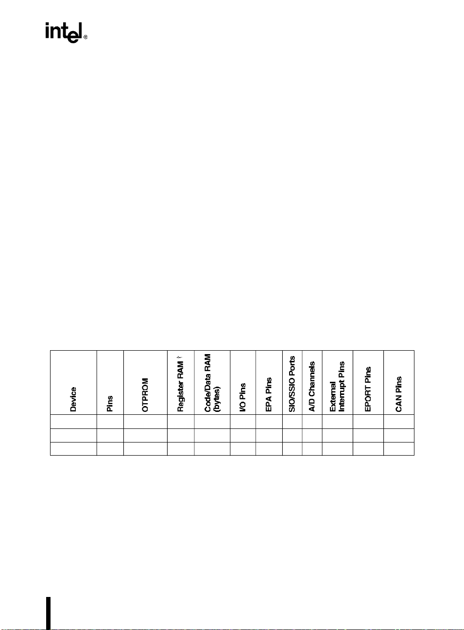
Table 2-1 lists the features of the 8XC196NT and the 87C196CB. The 87C196CB implements
more OTPROM, more register RAM, four additional A/D channels, and the CAN peripheral. The
100-pin 87C196CB also implements four additional EPORT pins.
Table 2-1. Features of the 8XC196NT and 87C196CB
8XC196NT 68 0 or 32 K 1 K 512 56 10 2 4 1 4 0
87C196CB 84 56 K 1.5 K 512 56 10 2 8 1 4 2
87C196CB 100 56 K 1.5 K 512 60 10 2 8 1 8 2
†
Register RAM amount includes the 24 bytes allocated to the core SFRs and stack pointer.
2-1
Page 17

87C196CB SUPPLEMENT
2.2 BLOCK DIAGRAM
Figure 2-1 shows the major blocks within the device. The 8XC196NT and 87C196CB have the
same peripheral set with the exception of the CAN (controller area network) periphe ral, which is
unique to the 87C196CB. The CAN peripheral manages communications between multiple network nodes. This integrated periph eral is similar to Intel’s standalon e 82527 CAN serial communications controller, supporting both the standard and extended message frames specified by the
CAN 2.0 protocol parts A and B.
Core
Clock and
Power Mgmt.
SSIO
OTPROM
Code/Data
RAM
EPAI/O
A/DSIO
Interrupt
Controller
PTS
WDT
Slave
Port
CAN
A3179-01
Figure 2-1. 87C196CB Block Diagram
2.3 INTERNAL TIMING
The 87C196CB’s clock circuitry ( Figure 2-2 ) implements phase-locked loop and clock multiplier
circuitry, which can substantially increase the CPU clock rate while using a lower-frequency input clock. The clock circuitry accepts an input clock signal on XTAL1 provided by an external
crystal or oscillator. Depending on the value of the PLLEN pin, this frequency is routed either
through the phase-locked loop and multiplier or directly to the divide-by-two circuit. The multiplier circuitry can quadruple the inpu t frequency (F
) before the frequency (f) reache s the di-
XTAL1
vide-by-two circuitry. The clock generators accept the divided input frequency (f/2) from the
divide-by-two circuit and produce two nonoverlapping internal timing signals, PH1 and PH2.
These signals are active when high.
2-2
NOTE
This manual uses lowercase “f” to represent the internal clock frequency. For
the 87C196CB, f is equal to either F
XTAL1
or 4F
, depending on the clock
XTAL1
multiplier mode, which is controlled by the PLLEN input pin.
Page 18

XTAL1
F
XTAL1
Disable
PLL
(Powerdown)
ARCHITECTURAL OVERVIEW
Phase
Comparator
Filter
Phase-
locked
Oscillator
Phase-locked Loop
Clock Multiplier
Peripheral Clocks (PH1, PH2)
CLKOUT
CPU Clocks (PH1, PH2)
A3168-01
XTAL2
PLLEN
Disable
Oscillator
(Powerdown)
XTAL1
F
XTAL1
4F
Disable Clock Input
(Powerdown)
f
Divide-by-two
Circuit
f
2
Clock
Generators
Disable Clocks
(Powerdown)
Disable Clocks
(Idle, Powerdown)
Figure 2-2. Clock Circuitry
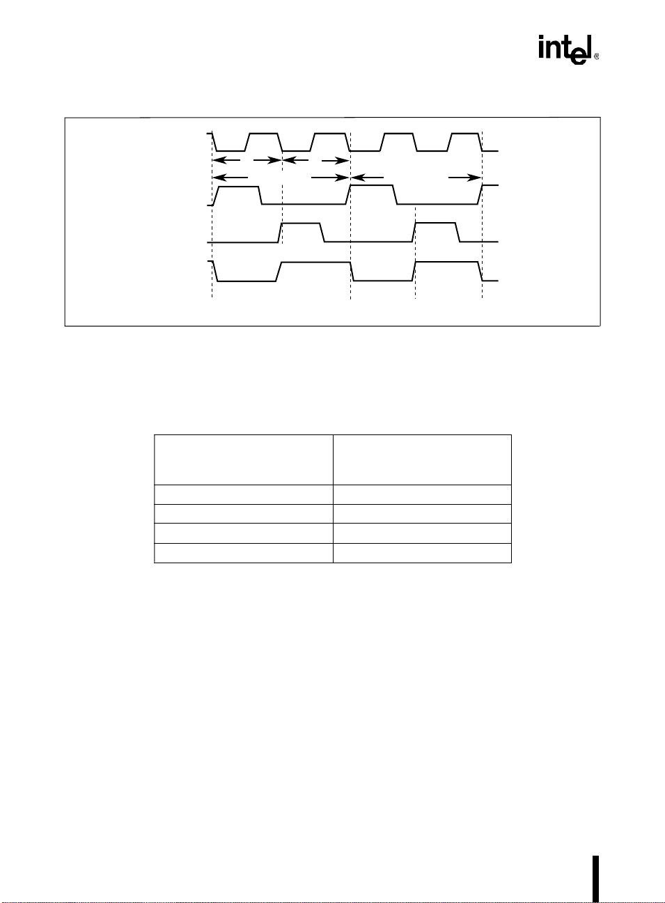
The rising edges of PH1 and PH2 generate the internal CLKOUT signal (Figure 2-3). The clock
circuitry routes separate internal clock signals to the CPU and the peripher als to provid e flexibility in power management. It also outputs the CLKOUT signal on the CLKOUT pin. Because of
the complex logic in the clock circuitry, the signal on the CLKOUT pin is a delayed version of
the internal CLKOUT signal. This delay varies with temperature and voltage.
2-3
Page 19
87C196CB SUPPLEMENT
XTAL1
PH1
PH2
CLKOUT
tt
1 State Time
1 State Time
Phase 1 Phase 2
Phase 1 Phase 2
A0805-01
Figure 2-3. Internal Clock Phases
The combined period of phase 1 and phase 2 of the internal CLKOUT signal defines the basic
time unit known as a state time or state. Table 2-2 lists state time durations at various frequencies.
Table 2-2. State Times at Various Frequencies
(Frequency Input to th e
Divide-by-two Circuit)
f
State Time
8 MHz 250 ns
12 MHz 167 ns
16 MHz 125 ns
20 MHz 100 ns
The following formulas calculate the freq uency of PH1 and PH2, the d uration of a state time, and
the duration of a clock period (t).
P H1 (in MHz)
f
-- - PH2== State Time (in µs)
2
2
-- -= t
f
1
-- -=
f
Because the device can operate at many frequencies, this manual defines time requir ements (such
as instruction execution times) in terms of state times rather than specific measurements.
Datasheets list AC characteristics in terms of clock periods (t; sometimes called T
osc
).
Figure 2-4 illustrates the timing relationships between the input freq uency (F
), the operating
XTAL1
frequency (f), and the CLKOUT signal with each PLLEN pin conf iguration. Ta ble 2-3 details the
relationships between the input frequency (F
), the PLLEN pin, the operating frequency (f),
XTAL1
the clock period (t), and state times.
2-4
Page 20

XTAL1 (5 MHz)
CLKOUT
XTAL1 (5 MHz)
CLKOUT
ARCHITECTURAL OVERVIEW
PLLEN = 0
t = 80ns
f
T
XHCH
PLLEN = 1
t = 20ns
f
T
XHCH
A3170-01
Figure 2-4. Effect of Clock Mode on CLKOUT Frequency
Table 2-3. Relationships Between Input Frequency, Clock Multiplier, and State Times
F
XTAL1
(Frequency
on XTAL1)
PLLEN Multiplier
(Input Frequency to
the Divide-by-two Circui t)
f
4 MHz 0 1 4 MHz 250 ns 500 ns
5 MHz 0 1 5 MHz 200 ns 400 ns
8 MHz 0 1 8 MHz 125 ns 250 ns
12 MHz 0 1 12 MHz 83.5 ns 167 ns
16 MHz 0 1 16 MHz 62.5 ns 125 ns
20 MHz 0 1 20 MHz 50 ns 100 ns
4 MHz 1 4 16 MHz 62.5 ns 125 ns
5 MHz 1 4 20 MHz 50 ns 100 ns
t
(Clock
Period)
State Time
2-5
Page 21

Page 22

Memory Partitions
3
Page 23

Page 24

CHAPTER 3
MEMORY PARTITIONS
This chapter describes the differences in the address space of the 87C196CB from that of the
8XC196NT. The 87C196CB has 56 Kbytes of one-time-programmable read-only memory (OTPROM), while the 8XC196NT is available with 32 Kbytes. The 87C196CB also has an additional
512 bytes of register RAM.
The 87C196CB is available in eith er an 84-p in or a 100-pin p ackage. Th e 84-pin 8 7C196CB, like
the 8XC196NT, has up to 2 0 external address lines, enabling access to 1 Mbyte of linear add ress
space. The 100-pin 87C196CB has four additional pin s available for ex ternal add ress lines. With
all 24 external address lines connected (A23:16 and AD15:0), the 100-pin 87 C196CB can access
16 Mbytes of linear address space.
3.1 MEMORY MAP, SPECIAL-FUNCTION REGISTERS, AND WINDOWING
Table 3-1 compares the register file addresses of the 8XC196NT and 87C196CB. Table 3-2 is a
memory map of the 87C196CB. Table 3-3 lists the 87C196CB’s peripheral SFRs (these are the
same as those of the 8XC196NT). Table 3-4 lists the CAN peripheral SFRs, which are unique to
the 87C196CB. Tables 3-5 through 3-9 provide the information necessary to window higher
memory into the lower register file for direct access.
Table 3-1. Register File Memory Addresses
Device and Hex
Address Range
CB NT
1DFF
1C00
03FF
0100
00FF
001A
0019
0018
0017
0000
.
.
— Register RAM Indirect, indexed, or windowed direct
03FF
0100
00FF
001A
0019
0018
0017
0000
Upper register file (register RAM) Indirect, indexed, or windowed direct
Lower register file (register RAM) Direct, indirect, or indexed
Lower register file (stack pointer) Direct, indirect, or indexed
Lower register file (CPU SFRs) Direct, indirect, or indexed
Description Addressing Modes
3-1
Page 25

87C196CB SUPPLEMENT
Table 3-2. 87C196CB Memory Map
Hex
Address
FFFFFF
FF2080
FF207F
FF2000
FF1FFF
FF0600
FF05FF
FF0400
FF03FF
FF0100
FF00FF
FF0000
FEFFFF
0F0000
0EFFFF
010000
00FFFF
002000
001FFF
001FE0
001FDF
001F00
001EFF
001E00
001DFF
001C00
001BFF
000600
0005FF
000400
0003FF
000100
0000FF
000000
†
For the 87C196CB, the program and special-purpose memory locations (FF2000-FFF FFFH) can reside
Program memory (After a device reset, the first instruction fetch
is from FF2080H)
Special purpose memory
External device (memory or I/O) connected to address/data bus Indirect, indexed, extended
Internal code and data RAM
(mapped identically into pages FFH and 00H)
External device (memory or I/O) connected to address/data bus Indirect, indexed, extended
Reserved
††
100-pin 87C196CB: External device (memory or I/O)
84-pin 87C196CB: Overlaid memory
External device (memory or I/O) connected to address/data bus Indirect, indexed, extended
External device or remapped OTPROM
Memory-mapped SFRs Indirect, indexed, extended
Peripheral SFRs
CAN SFRs Indirect, indexed, extended
Internal register RAM
External device (memory or I/O) connected to address/data bus;
future SFR expansion
Internal code and data RAM
(mapped identically into pages 00H and FFH)
Upper register file (register RAM)
Lower register file (register RAM, stack pointer, CPU SFRs) Direct, indirect, indexed
either in external memory or in internal OTPROM.
††
Locations xF0000-xF00FFH are reserved for in-circuit emulator s. Do not use these locations except to
initialize them. Except as otherwise noted, initialize unused program memory locations and reserved
memory locations to FFH.
†††
These locations can be either external memory (CCB2.2=0) or a copy of the OTPROM (CCB2.2=1).
Description Addressing Modes
†
†
Indirect, indexed, extended
Indirect, indexed, extended
Indirect, indexed, extended
Indirect, indexed, extended
††
†††
Indirect, indexed, extended
Indirect, indexed, extended
Indirect, indexed, extended,
windowed direct
Indirect, indexed,
windowed direct
Indirect, indexed, extended
Indirect, indexed, extended
Indirect, indexed,
windowed direct
3-2
Page 26

MEMORY PARTITIONS
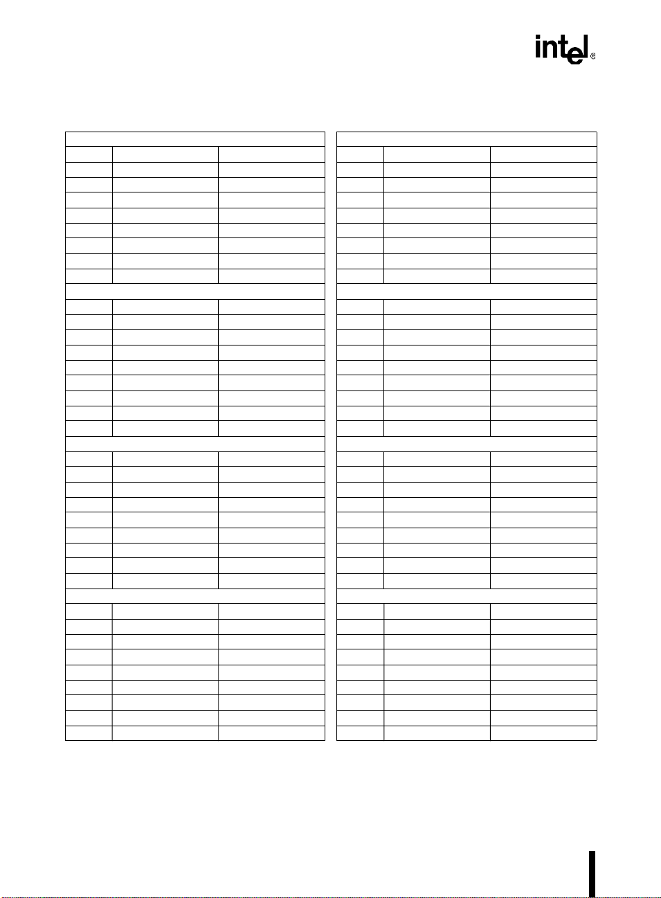
Table 3-3. 87C196CB Peripheral SFRs
Ports 0, 1, 2, and 6 SFRs Timer 1, Timer 2, and EPA SFRs
Address High (Odd) Byte Low (Even) Byte Address High (Odd) Byte Low (Even) Byte
1FDEH Reserved Reserved
1FDCH Reserved Reserved 1F9CH Reserved T2CON TROL
1FDAH Reserved P0_PIN
1FD8H Reserved Reserved 1F98H Reserved T1CONTROL
1FD6H P6_PIN P1_P IN 1F96H Reserved Reserved
1FD4H P6_REG P1_REG 1F94H Reserved Reserved
1FD2H P6_DIR P1_DIR 1F92H Reserved Reserved
1FD0H P6_MODE P1_MODE 1F90H Reserved Reserved
1FCEH P2_PIN Reserved EPA SFRs
1FCCH P2_REG Reserved
1FCAH P2_DIR Reserved
1FC8H P2_MODE Reserved 1F8CH Reserved COMP1_CON
1FC6H Reserved Reserved
1FC4H Reserved Reserved 1F88H Reserved COMP0_CON
1FC2H Reserved Reserved
1FC0H Reserved Reserved 1F84H Reserved EPA9_CON
SIO and SS IO SFRs
Address High (Odd) Byte Low (Even) Byte
1FBEH Reserved Reserved
1FBCH SP_BAUD (H) SP_BAUD (L) 1F7CH Reserved EPA7_CON
1FBAH SP_CON SBUF_TX
1FB8H SP_STATUS SBUF_RX 1F78H Reserved EPA6_CON
1FB6H Reserved Reserved
1FB4H Reserved SSIO_BAUD 1F74H Reserved EP A5_CON
1FB2H SSIO1_CON SSIO1_BUF
1FB0H SSIO0_CON SSIO0_BUF 1F70H Reserved EPA4_CON
A/D SFRs
Address High (Odd) Byte Low (Even) Byte
1FAEH AD_TIME AD_TEST
1FACH Reserved AD_COMMAND 1F68H Reserved EPA2_CON
1FAAH AD_RESULT (H) AD_RESULT (L)
EPA Interrupt SFRs
Address High (Odd) Byte Low (Even) Byte
1FA8H Reserved EPAIPV 1F60H Reserved EPA0_CON
1FA6H Reserved EPA_PEND1
1FA4H Reserved EPA_MASK1
†
1FA2H EPA_PEND (H) EPA_PEND (L)
†
1FA0H EP A_M AS K (H) EP A_M ASK (L)
†
Must be addressed as a word .
†
1F9EH TIMER2 (H) TIMER2 (L)
†
1F9AH TIMER1 (H) TIMER1 (L)
Address High (Odd) Byte Low (Even) Byte
†
1F8EH COMP1_TIME (H) COMP 1_TI M E (L)
†
1F8AH COMP0_TIME (H) COMP 0_TI M E (L)
†
1F86H EPA9_TIME (H) EPA9_TIME (L)
†
1F82H EPA8_TIME (H) EPA8_TIME (L)
1F80H Reserved EPA8_CON
†
1F7EH EPA7_TIME (H) EPA7_TIME (L)
†
1F7AH EPA6_TIME (H) EPA6_TIME (L)
†
1F76H EPA5_TIME (H) EPA5_TIME (L)
†
1F72H EPA4_TIME (H) EPA4_TIME (L)
†
1F6EH EPA3_TIME (H) EPA3_TIME (L)
†
1F6CH EPA3_CON (H) EPA3_CON (L)
†
1F6AH EPA2_TIME (H) EPA2_TIME (L)
†
1F66H EPA1_TIME (H) EPA1_TIME (L)
†
1F64H EPA1_CON (H) EPA1_CON (L)
†
1F62H EPA0_TIME (H) EPA0_TIME (L)
3-3
Page 27
87C196CB SUPPLEMENT
Table 3-4. CAN Peripheral SFRs
Message 15 Message 11
Addr High (Odd) Byte Low (Even) Byte Addr High (Odd) Byte Low (Even) Byte
1EFEH Reserved CAN_MSG15DATA7 1EBEH Reserved CAN_MSG11DATA7
1EFCH CAN_MSG15DATA6 CAN_MSG15DATA5 1EBCH CAN_MSG11DATA6 CAN_MSG11DATA5
1EFAH CAN_MSG15DATA4 CAN_MSG15DATA3 1EBAH CAN_MSG11DATA4 CAN_MSG11DATA3
1EF8H CAN_MSG15DATA2 CAN_MSG15DATA1 1EB8H CAN_MSG11DATA2 CAN_MSG11DATA1
1EF6H CAN_MSG15DATA0 CAN_MSG15CFG 1EB6H CAN_MSG11DATA0 CAN_MSG11CFG
1EF4H CAN_MSG15ID3 CAN_MSG15ID2 1EB4H CAN_MSG11ID3 CAN_MSG11ID2
1EF2H CAN_MSG15ID1 CAN_MSG15ID0 1EB2H CAN_MSG11ID1 CAN_MSG11ID0
1EF0H CAN_MSG15CON1 CAN_MSG15CON0 1EB0H CAN_MSG11CON1 CAN_MSG11CON0
Message 14 Message 10
Addr High (Odd) Byte Low (Even) Byte Addr High (Odd) Byte Low (Even) Byte
1EEEH Reserved CAN_MSG14DATA7 1EAEH Reserved CAN_MSG10DATA7
1EECH CAN_MSG14DATA6 CAN_MSG14DATA5 1EACH CAN_MSG10DATA6 CAN_MSG10DATA5
1EEAH CAN_MSG14DATA4 CAN_MSG14DATA3 1EAAH CAN_MSG10DATA4 CAN_MSG10DATA3
1EE8H CAN_MSG14DATA2 CAN_MSG14DATA1 1EA8H CAN_MSG10DATA2 CAN_MSG10DATA1
1EE6H CAN_MSG14DATA0 CAN_MSG14CFG 1EA6H CAN_MSG10DATA0 CAN_MSG10CFG
1EE4H CAN_MSG14ID3 CAN_MSG14ID2 1EA4H CAN_MSG10ID3 CAN_MSG10ID2
1EE2H CAN_MSG14ID1 CAN_MSG14ID0 1EA2H CAN_MSG10ID1 CAN_MSG10ID0
1EE0H CAN_MSG14CON1 CAN_MSG14CON0 1EA0H CAN_MSG10CON1 CAN_MSG10CON0
Message 13 Message 9
Addr High (Odd) Byte Low (Even) Byte Addr High (Odd) Byte Low (Even) Byte
1EDEH Reserved CAN_MSG13DATA7 1E9EH Reserved CAN_MSG9DATA7
1EDCH CAN_MSG13DATA6 CAN_MSG13DATA5 1E9CH CAN_MSG9D ATA6 CAN_MSG9DATA5
1EDAH CAN_MSG13DATA4 CAN_MSG13DATA3 1E9AH CAN_MSG9DATA4 CAN_MSG9DATA3
1ED8H CAN_MSG13DATA2 CAN_MSG13DATA1 1E98H CAN_MSG9DATA2 CAN_MSG9DATA1
1ED6H CAN_MSG13DATA0 CAN_MSG13CFG 1E96H CAN_MSG9DATA0 CAN_MSG9CFG
1ED4H CAN_MSG13ID3 CAN_MSG13ID2 1E94H CAN_MSG9ID3 CAN_MSG9ID2
1ED2H CAN_MSG13ID1 CAN_MSG13ID0 1E92H CAN_MSG9ID1 CAN_MSG9ID0
1ED0H CAN_MSG13CON1 CAN_MSG13CON0 1E90H CAN_MSG9CON1 CAN_MSG9CON0
Message 12 Message 8
Addr High (Odd) Byte Low (Even) Byte Addr High (Odd) Byte Low (Even) Byte
1ECEH Reserved CAN_MSG12DATA7 1E8EH Reserved CAN_MSG8DATA7
1ECCH CAN_MSG12DATA6 CAN_MSG12DATA5 1E8CH CAN_MSG8D ATA6 CAN_MSG8DATA5
1ECAH CAN_MSG12DATA4 CAN_MSG12DATA3 1E8AH CAN_MSG8DATA4 CAN_MSG8DATA3
1EC8H CAN_MSG12DATA2 CAN_MSG12DATA1 1E88H CAN_MSG8DATA2 CAN_MSG8DATA1
1EC6H CAN_MSG12DATA0 CAN_MSG12CFG 1E86H CAN_MSG8DATA0 CAN_MSG8CFG
1EC4H CAN_MSG12ID3 CAN_MSG12ID2 1E84H CAN_MSG8ID3 CAN_MSG8ID2
1EC2H CAN_MSG12ID1 CAN_MSG12ID0 1E82H CAN_MSG8ID1 CAN_MSG8ID0
1EC0H CAN_MSG12CON1 CAN_MSG12CON0 1E80H CAN_MSG8CON1 CAN_MSG8CON0
3-4
Page 28

MEMORY PARTITIONS
Table 3-4. CAN Peripheral SFRs (Continued)
Message 7 Message 3 and Bit Timing 0
Addr High (Odd) Byte Low (Even) Byte Addr High (Odd) Byte Low (Even) Byte
1E7EH Reserved CAN_MSG7DATA7 1E3EH CAN_BT IM E0
1E7CH C AN_MSG7DATA6 CAN_MSG7DATA5 1E3CH CAN_MSG3DATA6 CAN_MSG3 D ATA5
1E7AH CAN_MSG7DATA4 CAN_MSG7DATA3 1E3AH CAN_MSG3DATA4 CAN_MSG3DATA3
1E78H CAN_MSG7DATA2 CAN_MSG7DATA1 1E38H CAN_MSG3DATA2 CAN_MSG3DATA1
1E76H CAN_MSG7DATA0 CAN_MSG7CFG 1E36H CAN_M SG3D ATA0 CAN_MSG3CFG
1E74H CAN_MSG7ID3 CAN_MSG7ID2 1E34H CAN_MSG3ID3 CAN_MSG3ID2
1E72H CAN_MSG7ID1 CAN_MSG7ID0 1E32H CAN_MSG3ID1 CAN_MSG3ID0
1E70H CAN_MSG7CON1 CAN_MSG7CON0 1E30 H CAN_MSG3CON1 CAN_MSG3CON0
Message 6 Message 2
Addr High (Odd) Byte Low (Even) Byte Addr High (Odd) Byte Low (Even) Byte
1E6EH Reserved CAN_MSG6DATA7 1E2EH Reserved CAN_MSG2DATA7
1E6CH CAN_MSG6DATA6 CAN_MSG6DATA5 1E2CH CAN_MSG2DATA6 CAN_MSG2DATA5
1E6AH CAN_MSG6DATA4 CAN_MSG6DATA3 1E2AH CAN_MSG2DATA4 CAN_MSG2DATA3
1E68H CAN_MSG6DATA2 CAN_MSG6DATA1 1E28H CAN_MSG2DATA2 CAN_MSG2DATA1
1E66H CAN_MSG6DATA0 CAN_MSG6CFG 1E26H CAN_MSG2DATA0 CAN_MSG2CFG
1E64H CAN_MSG6ID3 CAN_MSG6ID2 1E24H CAN_MSG2ID3 CAN_MSG2ID2
1E62H CAN_MSG6ID1 CAN_MSG6ID0 1E22H CAN_MSG2ID1 CAN_MSG2ID0
1E60H CAN_MSG6CON1 CAN_MSG6CON0 1E20H CAN_MSG2CON1 CAN_MSG2CON0
Message 5 and Interrupts Message 1
Addr High (Odd) Byte Low (Even) Byte Addr High (Odd) Byte Low (Even) Byte
1E5EH CAN_INT CAN_MSG5DATA7 1E1EH Reserved CAN_MSG1DATA7
1E5CH CAN_MSG5DATA6 CAN_MSG5DATA5 1E1CH CAN_MSG1DATA6 CAN_MSG1DATA5
1E5AH CAN_MSG5DATA4 CAN_MSG5DATA3 1E1AH CAN_MSG1DATA4 CAN_MSG1DATA3
1E58H CAN_MSG5DATA2 CAN_MSG5DATA1 1E18H CAN_MSG1DATA2 CAN_MSG1DATA1
1E56H CAN_MSG5DATA0 CAN_MSG5CFG 1E16H CAN_MSG1DATA0 CAN_MSG1CFG
1E54H CAN_MSG5ID3 CAN_MSG5ID2 1E14H CAN_MSG1ID3 CAN_MSG1ID2
1E52H CAN_MSG5ID1 CAN_MSG5ID0 1E12H CAN_MSG1ID1 CAN_MSG1ID0
1E50H CAN_MSG5CON1 CAN_MSG5CON0 1E10H CAN_MSG1CON1 CAN_MSG1CON0
Message 4 and Bit Timing 1 Mask, Control, and Status
Addr High (Odd) Byte Low (Even) Byte Addr High (Odd) Byte Low (Even) Byte
1E4EH CAN_BTIME1
1E4CH CAN_MSG4DATA6 CAN_MSG4DATA5 1E0CH CAN_MSK15 CAN_MSK15
1E4AH CAN_MSG4DATA4 CAN_MSG4DATA3 1E0AH CAN_EGMSK CAN_EGMSK
1E48H CAN_MSG4DATA2 CAN_MSG4DATA1 1E08H CAN_EGMSK CAN_EGMSK
1E46H CAN_MSG4DATA0 CAN_MSG4CFG 1E06H CAN_SGMSK CAN_SGMSK
1E44H CAN_MSG4ID3 CAN_MSG4ID2 1E04H Reserved Reserved
1E42H CAN_MSG4ID1 CAN_MSG4ID0 1E02H Reserved Reserved
1E40H CAN_MSG4CON1 CAN_MSG4CON0 1E00H CAN_STAT CAN_CON
†
The CCE bit in the control register (CAN_CON) must be set to enable write access to the bit timing registers
(CAN_BTIME0 and CAN_BTIME1).
†
CAN_MSG4DATA7 1E0EH CAN_MSK15 CAN_MSK15
†
CAN_MSG3DATA7
†
3-5
Page 29

87C196CB SUPPLEMENT
Table 3-5. Selecting a Window of Peripheral SFRs
Peripheral
Ports 0, 1, 2, 6 7EH 3FH
EPA compare 0–1, capture/compare 8–9, timers 7CH
EPA capture/compare 0–7 7BH 3DH 1EH
CAN messages 14–15 77H
CAN messages 12–13 76H
CAN messages 10–11 75H
CAN messages 8–9 74H
CAN messages 6–7 73H
CAN messages 4–5, bit timing 1, interrupts 72H
CAN messages 2–3, bit timing 0 71H
CAN message 1, control, status, mask 70H
WSR Value for
32-byte Window
(00E0–00FFH)
WSR Value for
64-byte Window
(00C0–00FFH)
3EH
3BH
3AH
39H
38H
WSR Value for
128-byte Window
(0080–00FFH)
1FHA/D converter, EPA interrupts 7DH
1DH
1CH
3-6
Page 30

Table 3-6. Selecting a Window of the Upper Register File
Register RAM
Locations
03E0–03FFH 5FH
03C0–03DFH 5EH
03A0–03BFH 5DH
0380–039FH 5CH
0360–037FH 5BH
0340–035FH 5AH
0320–033FH 59H
0300–031FH 58H
02E0–02FFH 57H
02C0–02DFH 56H
02A0–02BFH 55H
0260–027FH 53H
0240–025FH 52H
0220–023FH 51H
01E0–01FFH 4FH
01C0–01DFH 4EH
01A0–01BFH 4DH
0160–017FH 4BH
0140–015FH 4AH
0120–013FH 49H
WSR Value
for 32-byte Window
(00E0–00FFH)
WSR Value
for 64-byte Window
(00C0–00FFH)
2FH
2EH
2DH
2CH
2BH
2AH0280–029FH 54H
29H
28H0200–021FH 50H
27H
26H0180–019FH 4CH
25H
24H0100–011FH 48H
MEMORY PARTITIONS
WSR Value
for 128-byte Window
(0080–00FFH)
17H
16H
15H
14H
13H
12H
3-7
Page 31

87C196CB SUPPLEMENT
3-8
Page 32

Table 3-7. Selecting a Window of Upper Register RAM
Register RAM
Locations
0DE0–0DFFH 6FH
0DC0–0DDFH 6EH
0DA0–0DBFH 6DH
0D80–0D9FH 6CH
0D60–0D7FH 6BH
0D40–0D5FH 6AH
0D20–0D3FH 69H
0D00–0D1FH 68H
0CE0–0CFFH 67H
0CC0–0CDFH 66H
0CA0–0CBFH 65H
0C80–0C9FH 64H
0C60–0C7FH 63H
0C40–0C5FH 62H
0C20–0C3FH 61H
0C00–0C1FH 60H
WSR Value
for 32-byte Window
(00E0–00FFH)
WSR Value
for 64-byte Window
(00C0–00FFH)
37H
36H
35H
34H
33H
32H
31H
30H
MEMORY PARTITIONS
WSR Value
for 128-byte Window
(0080–00FFH)
1BH
1AH
19H
18H
3-9
Page 33

87C196CB SUPPLEMENT
Table 3-8. Windows
Base Address
WSR Value
for 32-byte Window
(00E0–00FFH)
WSR Value
for 64-byte Window
(00C0–00FFH)
Peripheral SFRs
1FE0H 7FH
1FC0H 7EH
†
†
3FH
1FA0H 7DH
3EH1F80H 7CH
1F60H 7BH
1F40H 7AH
3DH
1F20H 79H
3CH1F00H 78H
CAN Peripheral SFRs
1EE0H 77H
1EC0H 76H
3BH
1EA0H 75H
3AH1E80H 74H
1E60H 73H
1E40H 72H
39H
1E20H 71H
38H1E00H 70H
Register RAM
1DE0H 6FH
1DC0H 6EH
37H
1DA0H 6DH
36H1D80H 6CH
1D60H 6BH
1D40H 6AH
35H
1D20H 69H
34H1D00H 68H
1CE0H 67H
1CC0H 66H
33H
1CA0H 65H
32H1C80H 64H
1C60H 63H
1C40H 62H
31H
1C20H 61H
30H1C00H 60H
†
Locations 1FE0–1FFFH contain memory-mapped SFRs that cannot be access ed through a window.
Reading these locations through a window returns FFH; writing these locations through a window has no
effect.
WSR Value for
128-byte Window
(0080–00FFH)
†
1FH
1EH
1DH
1CH
1BH
1AH
19H
18H
3-10
Page 34

MEMORY PARTITIONS
Table 3-8. Windows (Continued)
Base Address
Upper Register File
03E0H 5FH
03C0H 5EH
03A0H 5DH
0360H 5BH
0340H 5AH
0320H 59H
02E0H 57H
02C0H 56H
02A0H 55H
0260H 53H
0240H 52H
0220H 51H
01E0H 4FH
01C0H 4EH
01A0H 4DH
0160H 4BH
0140H 4AH
0120H 49H
†
Locations 1FE0–1FFFH contain memory-mapped SFRs that cannot be access ed through a window.
Reading these locations through a window returns FFH; writing these locations through a window has no
effect.
WSR Value
for 32-byte Window
(00E0–00FFH)
WSR Value
for 64-byte Window
(00C0–00FFH)
2FH
2EH0380H 5CH
2DH
2CH0300H 58H
2BH
2AH0280H 54H
29H
28H0200H 50H
27H
26H0180H 4CH
25H
24H0100H 48H
WSR Value for
128-byte Window
(0080–00FFH)
17H
16H
15H
14H
13H
12H
3-11
Page 35

87C196CB SUPPLEMENT
Table 3-9 . WSR Settings and Direct Address es for Windowable SFRs
32-byte Windows
Register Mnemonic
AD_COMMAND 1FACH 7DH 00ECH 3EH 00ECH 1FH 00ACH
AD_RESULT 1FAAH 7DH 00EAH 3EH 00EAH 1FH 00AAH
AD_TEST 1FAEH 7DH 00EEH 3EH 00EEH 1FH 00AEH
AD_TIME 1FAFH 7DH 00EFH 3EH 00EFH 1FH 00AFH
CAN_BTIME0 1E3FH 71H 00FFH 38H 00FFH 1CH 00BFH
CAN_BTIME1 1E4FH 72H 00EFH 39H 00CFH 1CH 00CFH
CAN_CON 1E00H 70H 00E0H 38H 00C0H 1CH 0080H
CAN_EGMSK 1E08H 70H 00E8H 38H 00C8H 1CH 0088H
CAN_INT 1E5FH 72H 00FFH 39H 00DFH 1CH 00DFH
CAN_MSG1CFG 1E16H 70H 00F6H 38H 00D6H 1CH 0096H
CAN_MSG2CFG 1E26H 71H 00E6H 38H 00E6H 1CH 00A6H
CAN_MSG3CFG 1E36H 71H 00F6H 38H 00F6H 1CH 00B6H
CAN_MSG4CFG 1E46H 72H 00E6H 39H 00C6H 1CH 00C6H
CAN_MSG5CFG 1E56H 72H 00F6H 39H 00D6H 1CH 00D6H
CAN_MSG6CFG 1E66H 73H 00E6H 39H 00E6H 1CH 00E6H
CAN_MSG7CFG 1E76H 73H 00F6H 39H 00F6H 1CH 00F6H
CAN_MSG8CFG 1E86H 74H 00E6H 3AH 00C6H 1DH 0086H
CAN_MSG9CFG 1E96H 74H 00F6H 3AH 00D6H 1DH 0096H
CAN_MSG10CFG 1EA6H 75H 00E6H 3AH 00E6H 1DH 00A6H
CAN_MSG11CFG 1EB6H 75H 00F6H 3AH 00F6H 1DH 00B6H
CAN_MSG12CFG 1EC6H 76H 00E6H 3BH 00C6H 1DH 00C6H
CAN_MSG13CFG 1ED6H 76H 00F6H 3BH 00D6H 1DH 00D6H
CAN_MSG14CFG 1EE6H 77H 00E6H 3BH 00E6H 1DH 00E6H
CAN_MSG15CFG 1EF6H 77H 00F6H 3BH 00F6H 1DH 00F6H
CAN_MSG1CON0 1E10H 70H 00F0H 38H 00D0H 1CH 0090H
CAN_MSG2CON0 1E20H 71H 00E0H 38H 00E0H 1CH 00A0H
CAN_MSG3CON0 1E30H 71H 00F0H 38H 00F0H 1CH 00B0H
CAN_MSG4CON0 1E40H 72H 00E0H 39H 00C0H 1CH 00C0H
CAN_MSG5CON0 1E50H 72H 00F0H 39H 00D0H 1CH 00D0H
CAN_MSG6CON0 1E60H 73H 00E0H 39H 00E0H 1CH 00E0H
†
Must be addressed as a word.
Memory
Location
(00E0–00FFH)
WSR
Address
Direct
64-byte Windows
(00C0–00FFH)
WSR
Direct
Address
128-byte Windows
(0080–00FFH)
WSR
Direct
Address
3-12
Page 36

MEMORY PARTITIONS
Table 3-9. WSR Settings and Direct Addresses for Windowable SFRs (Continued)
32-byte Windows
Register Mnemonic
CAN_MSG7CON0 1E70H 73H 00F0H 39H 00F0H 1CH 00F0H
CAN_MSG8CON0 1E80H 74H 00E0H 3AH 00C0H 1DH 0080H
CAN_MSG9CON0 1E90H 74H 00F0H 3AH 00D0H 1DH 0090H
CAN_MSG10CON0 1EA0H 75H 00E0H 3AH 00E0H 1DH 00A0H
CAN_MSG11CON0 1EB0H 75H 00F0H 3AH 00F0H 1DH 00B0H
CAN_MSG12CON0 1EC0H 76H 00E0H 3BH 00C0H 1DH 00C0H
CAN_MSG13CON0 1ED0H 76H 00F0H 3BH 00D0H 1DH 00D0H
CAN_MSG14CON0 1EE0H 77H 00E0H 3BH 00E0H 1DH 00E0H
CAN_MSG15CON0 1EF0H 77H 00F0H 3BH 00F0H 1DH 00F0H
CAN_MSG1CON1 1E11H 70H 00F1H 38H 00D1H 1CH 0091H
CAN_MSG2CON1 1E21H 71H 00E1H 38H 00E1H 1CH 00A1H
CAN_MSG3CON1 1E31H 71H 00F1H 38H 00F1H 1CH 00B1H
CAN_MSG4CON1 1E41H 72H 00E1H 39H 00C1H 1CH 00C1H
CAN_MSG5CON1 1E51H 72H 00F1H 39H 00D1H 1CH 00D1H
CAN_MSG6CON1 1E61H 73H 00E1H 39H 00E1H 1CH 00E1H
CAN_MSG7CON1 1E71H 73H 00F1H 39H 00F1H 1CH 00F1H
CAN_MSG8CON1 1E81H 74H 00E1H 3AH 00C1H 1DH 0081H
CAN_MSG9CON1 1E91H 74H 00F1H 3AH 00D1H 1DH 0091H
CAN_MSG10CON1 1EA1H 75H 00E1H 3AH 00E1H 1DH 00A1H
CAN_MSG11CON1 1EB1H 75H 00F1H 3AH 00F1H 1DH 00B1H
CAN_MSG12CON1 1EC1H 76H 00E1H 3BH 00C1H 1DH 00C1H
CAN_MSG13CON1 1ED1H 76H 00F1H 3BH 00D1H 1DH 00D1H
CAN_MSG14CON1 1EE1H 77H 00E1H 3BH 00E1H 1DH 00E1H
CAN_MSG15CON1 1EF1H 77H 00F1H 3BH 00F1H 1DH 00F1H
CAN_MSG1DATA0 1E17H 70H 00F7H 38H 00D7H 1CH 0097H
CAN_MSG2DATA0 1E27H 71H 00E7H 38H 00E7H 1CH 00A7H
CAN_MSG3DATA0 1E37H 71H 00F7H 38H 00F7H 1CH 00B7H
CAN_MSG4DATA0 1E47H 72H 00E7H 39H 00C7H 1CH 00C7H
CAN_MSG5DATA0 1E57H 72H 00F7H 39H 00D7H 1CH 00D7H
CAN_MSG6DATA0 1E67H 73H 00E7H 39H 00E7H 1CH 00E7H
CAN_MSG7DATA0 1E77H 73H 00F7H 39H 00F7H 1CH 00F7H
CAN_MSG8DATA0 1E87H 74H 00E7H 3AH 00C7H 1DH 0087H
†
Must be addressed as a word.
Memory
Location
(00E0–00FFH)
WSR
Address
Direct
64-byte Windows
(00C0–00FFH)
WSR
Direct
Address
128-byte Windows
(0080–00FFH)
WSR
Direct
Address
3-13
Page 37

87C196CB SUPPLEMENT
Table 3-9. WSR Settings and Direct Addresses for Windowable SFRs (Continued)
32-byte Windows
Register Mnemonic
CAN_MSG9DATA0 1E97H 74H 00F7H 3AH 00D7H 1DH 0097H
CAN_MSG10DATA0 1EA7H 75H 00E7H 3AH 00E7H 1DH 00A7H
CAN_MSG11DATA0 1EB7H 75H 00F7H 3AH 00F7H 1DH 00B7H
CAN_MSG12DATA0 1EC7H 76H 00E7H 3BH 00C7H 1DH 00C7H
CAN_MSG13DATA0 1ED7H 76H 00F7H 3BH 00D7H 1DH 00D7H
CAN_MSG14DATA0 1EE7H 77H 00E7H 3BH 00E7H 1DH 00E7H
CAN_MSG15DATA0 1EF7H 77H 00F7H 3BH 00F7H 1DH 00F7H
CAN_MSG1DATA1 1E18H 70H 00F8H 38H 00D8H 1CH 0098H
CAN_MSG2DATA1 1E28H 71H 00E8H 38H 00E8H 1CH 00A8H
CAN_MSG3DATA1 1E38H 71H 00F8H 38H 00F8H 1CH 00B8H
CAN_MSG4DATA1 1E48H 72H 00E8H 39H 00C8H 1CH 00C8H
CAN_MSG5DATA1 1E58H 72H 00F8H 39H 00D8H 1CH 00D8H
CAN_MSG6DATA1 1E68H 73H 00E8H 39H 00E8H 1CH 00E8H
CAN_MSG7DATA1 1E78H 73H 00F8H 39H 00F8H 1CH 00F8H
CAN_MSG8DATA1 1E88H 74H 00E8H 3AH 00C8H 1DH 0088H
CAN_MSG9DATA1 1E98H 74H 00F8H 3AH 00D8H 1DH 0098H
CAN_MSG10DATA1 1EA8H 75H 00E8H 3AH 00E8H 1DH 00A8H
CAN_MSG11DATA1 1EB8H 75H 00F8H 3AH 00F8H 1DH 00B8H
CAN_MSG12DATA1 1EC8H 76H 00E8H 3BH 00C8H 1DH 00C8H
CAN_MSG13DATA1 1ED8H 76H 00F8H 3BH 00D8H 1DH 00D8H
CAN_MSG14DATA1 1EE8H 77H 00E8H 3BH 00E8H 1DH 00E8H
CAN_MSG15DATA1 1EF8H 77H 00F8H 3BH 00F8H 1DH 00F8H
CAN_MSG1DATA2 1E19H 70H 00F9H 38H 00D9H 1CH 0099H
CAN_MSG2DATA2 1E29H 71H 00E9H 38H 00E9H 1CH 00A9H
CAN_MSG3DATA2 1E39H 71H 00F9H 38H 00F9H 1CH 00B9H
CAN_MSG4DATA2 1E49H 72H 00E9H 39H 00C9H 1CH 00C9H
CAN_MSG5DATA2 1E59H 72H 00F9H 39H 00D9H 1CH 00D9H
CAN_MSG6DATA2 1E69H 73H 00E9H 39H 00E9H 1CH 00E9H
CAN_MSG7DATA2 1E79H 73H 00F9H 39H 00F9H 1CH 00F9H
CAN_MSG8DATA2 1E89H 74H 00E9H 3AH 00C9H 1DH 0089H
CAN_MSG9DATA2 1E99H 74H 00F9H 3AH 00D9H 1DH 0099H
CAN_MSG10DATA2 1EA9H 75H 00E9H 3AH 00E9H 1DH 00A9H
†
Must be addressed as a word.
Memory
Location
(00E0–00FFH)
WSR
Address
Direct
64-byte Windows
(00C0–00FFH)
WSR
Direct
Address
128-byte Windows
(0080–00FFH)
WSR
Direct
Address
3-14
Page 38

MEMORY PARTITIONS
Table 3-9. WSR Settings and Direct Addresses for Windowable SFRs (Continued)
32-byte Windows
Register Mnemonic
CAN_MSG11DATA2 1EB9H 75H 00F9H 3AH 00F9H 1DH 00B9H
CAN_MSG12DATA2 1EC9H 76H 00E9H 3BH 00C9H 1DH 00C9H
CAN_MSG13DATA2 1ED9H 76H 00F9H 3BH 00D9H 1DH 00D9H
CAN_MSG14DATA2 1EE9H 77H 00E9H 3BH 00E9H 1DH 00E9H
CAN_MSG15DATA2 1EF9H 77H 00F9H 3BH 00F9H 1DH 00F9H
CAN_MSG1DATA3 1E1AH 70H 00FAH 38H 00DAH 1CH 009AH
CAN_MSG2DATA3 1E2AH 71H 00EAH 38H 00EAH 1CH 00AAH
CAN_MSG3DATA3 1E3AH 71H 00FAH 38H 00FAH 1CH 00BAH
CAN_MSG4DATA3 1E4AH 72H 00EAH 39H 00CAH 1CH 00CAH
CAN_MSG5DATA3 1E5AH 72H 00FAH 39H 00DAH 1CH 00DAH
CAN_MSG6DATA3 1E6AH 73H 00EAH 39H 00EAH 1CH 00EAH
CAN_MSG7DATA3 1E7AH 73H 00FAH 39H 00FAH 1CH 00FAH
CAN_MSG8DATA3 1E8AH 74H 00EAH 3AH 00CAH 1DH 008AH
CAN_MSG9DATA3 1E9AH 74H 00FAH 3AH 00DAH 1DH 009AH
CAN_MSG10DATA3 1EAAH 75H 00EAH 3AH 00EAH 1DH 00AAH
CAN_MSG11DATA3 1EBAH 75H 00FAH 3AH 00FAH 1DH 00BAH
CAN_MSG12DATA3 1ECAH 76H 00EAH 3BH 00CAH 1DH 00CAH
CAN_MSG13DATA3 1EDAH 76H 00FAH 3BH 00DAH 1DH 00DAH
CAN_MSG14DATA3 1EEAH 77H 00EAH 3BH 00EAH 1DH 00EAH
CAN_MSG15DATA3 1EFAH 77H 00FAH 3BH 00FAH 1DH 00FAH
CAN_MSG1DATA4 1E1BH 70H 00FBH 38H 00DBH 1CH 009BH
CAN_MSG2DATA4 1E2BH 71H 00EBH 38H 00EBH 1CH 00ABH
CAN_MSG3DATA4 1E3BH 71H 00FBH 38H 00FBH 1CH 00BBH
CAN_MSG4DATA4 1E4BH 72H 00EBH 39H 00CBH 1CH 00CBH
CAN_MSG5DATA4 1E5BH 72H 00FBH 39H 00DBH 1CH 00DBH
CAN_MSG6DATA4 1E6BH 73H 00EBH 39H 00EBH 1CH 00EBH
CAN_MSG7DATA4 1E7BH 73H 00FBH 39H 00FBH 1CH 00FBH
CAN_MSG8DATA4 1E8BH 74H 00EBH 3AH 00CBH 1DH 008BH
CAN_MSG9DATA4 1E9BH 74H 00FBH 3AH 00DBH 1DH 009BH
CAN_MSG10DATA4 1EABH 75H 00EBH 3AH 00EBH 1DH 00ABH
CAN_MSG11DATA4 1EBBH 75H 00FBH 3AH 00FBH 1DH 00BBH
CAN_MSG12DATA4 1ECBH 76H 00EBH 3BH 00CBH 1DH 00CBH
†
Must be addressed as a word.
Memory
Location
(00E0–00FFH)
WSR
Address
Direct
64-byte Windows
(00C0–00FFH)
WSR
Direct
Address
128-byte Windows
(0080–00FFH)
WSR
Direct
Address
3-15
Page 39

87C196CB SUPPLEMENT
Table 3-9. WSR Settings and Direct Addresses for Windowable SFRs (Continued)
32-byte Windows
Register Mnemonic
CAN_MSG13DATA4 1EDBH 76H 00FBH 3BH 00DBH 1DH 00DBH
CAN_MSG14DATA4 1EEBH 77H 00EBH 3BH 00EBH 1DH 00EBH
CAN_MSG15DATA4 1EFBH 77H 00FBH 3BH 00FBH 1DH 00FBH
CAN_MSG1DATA5 1E1CH 70H 00FCH 38H 00DCH 1CH 009CH
CAN_MSG2DATA5 1E2CH 71H 00ECH 38H 00ECH 1CH 00ACH
CAN_MSG3DATA5 1E3CH 71H 00FCH 38H 00FCH 1CH 00BCH
CAN_MSG4DATA5 1E4CH 72H 00ECH 39H 00CCH 1CH 00CCH
CAN_MSG5DATA5 1E5CH 72H 00FCH 39H 00DCH 1CH 00DCH
CAN_MSG6DATA5 1E6CH 73H 00ECH 39H 00ECH 1CH 00ECH
CAN_MSG7DATA5 1E7CH 73H 00FCH 39H 00FCH 1CH 00FCH
CAN_MSG8DATA5 1E8CH 74H 00ECH 3AH 00CCH 1DH 008CH
CAN_MSG9DATA5 1E9CH 74H 00FCH 3AH 00DCH 1DH 009CH
CAN_MSG10DATA5 1EACH 75H 00ECH 3AH 00ECH 1DH 00ACH
CAN_MSG11DATA5 1EBCH 75H 00FCH 3AH 00FCH 1DH 00BCH
CAN_MSG12DATA5 1ECCH 76H 00ECH 3BH 00CCH 1DH 00CCH
CAN_MSG13DATA5 1EDCH 76H 00FCH 3BH 00DCH 1DH 00DCH
CAN_MSG14DATA5 1EECH 77H 00ECH 3BH 00ECH 1DH 00ECH
CAN_MSG15DATA5 1EFCH 77H 00FCH 3BH 00FCH 1DH 00FCH
CAN_MSG1DATA6 1E1DH 70H 00FDH 38H 00DDH 1CH 009DH
CAN_MSG2DATA6 1E2DH 71H 00EDH 38H 00EDH 1CH 00ADH
CAN_MSG3DATA6 1E3DH 71H 00FDH 38H 00FDH 1CH 00BDH
CAN_MSG4DATA6 1E4DH 72H 00EDH 39H 00CDH 1CH 00CDH
CAN_MSG5DATA6 1E5DH 72H 00FDH 39H 00DDH 1CH 00DDH
CAN_MSG6DATA6 1E6DH 73H 00EDH 39H 00EDH 1CH 00EDH
CAN_MSG7DATA6 1E7DH 73H 00FDH 39H 00FDH 1CH 00FDH
CAN_MSG8DATA6 1E8DH 74H 00EDH 3AH 00CDH 1DH 008DH
CAN_MSG9DATA6 1E9DH 74H 00FDH 3AH 00DDH 1DH 009DH
CAN_MSG10DATA6 1EADH 75H 00EDH 3AH 00EDH 1DH 00ADH
CAN_MSG11DATA6 1EBDH 75H 00FDH 3AH 00FDH 1DH 00BDH
CAN_MSG12DATA6 1ECDH 76H 00EDH 3BH 00CDH 1DH 00CDH
CAN_MSG13DATA6 1EDDH 76H 00FDH 3BH 00DDH 1DH 00DDH
CAN_MSG14DATA6 1EEDH 77H 00EDH 3BH 00EDH 1DH 00EDH
†
Must be addressed as a word.
Memory
Location
(00E0–00FFH)
WSR
Address
Direct
64-byte Windows
(00C0–00FFH)
WSR
Direct
Address
128-byte Windows
(0080–00FFH)
WSR
Direct
Address
3-16
Page 40

MEMORY PARTITIONS
Table 3-9. WSR Settings and Direct Addresses for Windowable SFRs (Continued)
32-byte Windows
Register Mnemonic
CAN_MSG15DATA6 1EFDH 77H 00FDH 3BH 00FDH 1DH 00FDH
CAN_MSG1DATA7 1E1EH 70H 00FEH 38H 00DEH 1CH 009EH
CAN_MSG2DATA7 1E2EH 71H 00EEH 38H 00EEH 1CH 00AEH
CAN_MSG3DATA7 1E3EH 71H 00FEH 38H 00FEH 1CH 00BEH
CAN_MSG4DATA7 1E4EH 72H 00EEH 39H 00CEH 1CH 00CEH
CAN_MSG5DATA7 1E5EH 72H 00FEH 39H 00DEH 1CH 00DEH
CAN_MSG6DATA7 1E6EH 73H 00EEH 39H 00EEH 1CH 00EEH
CAN_MSG7DATA7 1E7EH 73H 00FEH 39H 00FEH 1CH 00FEH
CAN_MSG8DATA7 1E8EH 74H 00EEH 3AH 00CEH 1DH 008EH
CAN_MSG9DATA7 1E9EH 74H 00FEH 3AH 00DEH 1DH 009EH
CAN_MSG10DATA7 1EAEH 75H 00EEH 3AH 00EEH 1DH 00AEH
CAN_MSG11DATA7 1EBEH 75H 00FEH 3AH 00FEH 1DH 00BEH
CAN_MSG12DATA7 1ECEH 76H 00EEH 3BH 00CEH 1DH 00CEH
CAN_MSG13DATA7 1EDEH 76H 00FEH 3BH 00DEH 1DH 00DEH
CAN_MSG14DATA7 1EEEH 77H 00EEH 3BH 00EEH 1DH 00EEH
CAN_MSG15DATA7 1EFEH 77H 00FEH 3BH 00FEH 1DH 00FEH
CAN_MSG1ID0 1E12H 70H 00F2H 38H 00D2H 1CH 0092H
CAN_MSG2ID0 1E22H 71H 00E2H 38H 00E2H 1CH 00A2H
CAN_MSG3ID0 1E32H 71H 00F2H 38H 00F2H 1CH 00B2H
CAN_MSG4ID0 1E42H 72H 00E2H 39H 00C2H 1CH 00C2H
CAN_MSG5ID0 1E52H 72H 00F2H 39H 00D2H 1CH 00D2H
CAN_MSG6ID0 1E62H 73H 00E2H 39H 00E2H 1CH 00E2H
CAN_MSG7ID0 1E72H 73H 00F2H 39H 00F2H 1CH 00F2H
CAN_MSG8ID0 1E82H 74H 00E2H 3AH 00C2H 1DH 0082H
CAN_MSG9ID0 1E92H 74H 00F2H 3AH 00D2H 1DH 0092H
CAN_MSG10ID0 1EA2H 75H 00E2H 3AH 00E2H 1DH 00A2H
CAN_MSG11ID0 1EB2H 75H 00F2H 3AH 00F2H 1DH 00B2H
CAN_MSG12ID0 1EC2H 76H 00E2H 3BH 00C2H 1DH 00C2H
CAN_MSG13ID0 1ED2H 76H 00F2H 3BH 00D2H 1DH 00D2H
CAN_MSG14ID0 1EE2H 77H 00E2H 3BH 00E2H 1DH 00E2H
CAN_MSG15ID0 1EF2H 77H 00F2H 3BH 00F2H 1DH 00F2H
CAN_MSG1ID1 1E13H 70H 00F3H 38H 00D3H 1CH 0093H
†
Must be addressed as a word.
Memory
Location
(00E0–00FFH)
WSR
Address
Direct
64-byte Windows
(00C0–00FFH)
WSR
Direct
Address
128-byte Windows
(0080–00FFH)
WSR
Direct
Address
3-17
Page 41

87C196CB SUPPLEMENT
Table 3-9. WSR Settings and Direct Addresses for Windowable SFRs (Continued)
32-byte Windows
Register Mnemonic
CAN_MSG2ID1 1E23H 71H 00E3H 38H 00E3H 1CH 00A3H
CAN_MSG3ID1 1E33H 71H 00F3H 38H 00F3H 1CH 00B3H
CAN_MSG4ID1 1E43H 72H 00E3H 39H 00C3H 1CH 00C3H
CAN_MSG5ID1 1E53H 72H 00F3H 39H 00D3H 1CH 00D3H
CAN_MSG6ID1 1E63H 73H 00E3H 39H 00E3H 1CH 00E3H
CAN_MSG7ID1 1E73H 73H 00F3H 39H 00F3H 1CH 00F3H
CAN_MSG8ID1 1E83H 74H 00E3H 3AH 00C3H 1DH 0083H
CAN_MSG9ID1 1E93H 74H 00F3H 3AH 00D3H 1DH 0093H
CAN_MSG10ID1 1EA3H 75H 00E3H 3AH 00E3H 1DH 00A3H
CAN_MSG11ID1 1EB3H 75H 00F3H 3AH 00F3H 1DH 00B3H
CAN_MSG12ID1 1EC3H 76H 00E3H 3BH 00C3H 1DH 00C3H
CAN_MSG13ID1 1ED3H 76H 00F3H 3BH 00D3H 1DH 00D3H
CAN_MSG14ID1 1EE3H 77H 00E3H 3BH 00E3H 1DH 00E3H
CAN_MSG15ID1 1EF3H 77H 00F3H 3BH 00F3H 1DH 00F3H
CAN_MSG1ID2 1E14H 70H 00F4H 38H 00D4H 1CH 0094H
CAN_MSG2ID2 1E24H 71H 00E4H 38H 00E4H 1CH 00A4H
CAN_MSG3ID2 1E34H 71H 00F4H 38H 00F4H 1CH 00B4H
CAN_MSG4ID2 1E44H 72H 00E4H 39H 00C4H 1CH 00C4H
CAN_MSG5ID2 1E54H 72H 00F4H 39H 00D4H 1CH 00D4H
CAN_MSG6ID2 1E64H 73H 00E4H 39H 00E4H 1CH 00E4H
CAN_MSG7ID2 1E74H 73H 00F4H 39H 00F4H 1CH 00F4H
CAN_MSG8ID2 1E84H 74H 00E4H 3AH 00C4H 1DH 0084H
CAN_MSG9ID2 1E94H 74H 00F4H 3AH 00D4H 1DH 0094H
CAN_MSG10ID2 1EA4H 75H 00E4H 3AH 00E4H 1DH 00A4H
CAN_MSG11ID2 1EB4H 75H 00F4H 3AH 00F4H 1DH 00B4H
CAN_MSG12ID2 1EC4H 76H 00E4H 3BH 00C4H 1DH 00C4H
CAN_MSG13ID2 1ED4H 76H 00F4H 3BH 00D4H 1DH 00D4H
CAN_MSG14ID2 1EE4H 77H 00E4H 3BH 00E4H 1DH 00E4H
CAN_MSG15ID2 1EF4H 77H 00F4H 3BH 00F4H 1DH 00F4H
CAN_MSG1ID3 1E15H 70H 00F5H 38H 00D5H 1CH 0095H
CAN_MSG2ID3 1E25H 71H 00E5H 38H 00E5H 1CH 00A5H
CAN_MSG3ID3 1E35H 71H 00F5H 38H 00F5H 1CH 00B5H
†
Must be addressed as a word.
Memory
Location
(00E0–00FFH)
WSR
Address
Direct
64-byte Windows
(00C0–00FFH)
WSR
Direct
Address
128-byte Windows
(0080–00FFH)
WSR
Direct
Address
3-18
Page 42

MEMORY PARTITIONS
Table 3-9. WSR Settings and Direct Addresses for Windowable SFRs (Continued)
32-byte Windows
Register Mnemonic
Memory
Location
(00E0–00FFH)
WSR
Address
Direct
CAN_MSG4ID3 1E45H 72H 00E5H 39H 00C5H 1CH 00C5H
CAN_MSG5ID3 1E55H 72H 00F5H 39H 00D5H 1CH 00D5H
CAN_MSG6ID3 1E65H 73H 00E5H 39H 00E5H 1CH 00E5H
CAN_MSG7ID3 1E75H 73H 00F5H 39H 00F5H 1CH 00F5H
CAN_MSG8ID3 1E85H 74H 00E5H 3AH 00C5H 1DH 0085H
CAN_MSG9ID3 1E95H 74H 00F5H 3AH 00D5H 1DH 0095H
CAN_MSG10ID3 1EA5H 75H 00E5H 3AH 00E5H 1DH 00A5H
CAN_MSG11ID3 1EB5H 75H 00F5H 3AH 00F5H 1DH 00B5H
CAN_MSG12ID3 1EC5H 76H 00E5H 3BH 00C5H 1DH 00C5H
CAN_MSG13ID3 1ED5H 76H 00F5H 3BH 00D5H 1DH 00D5H
CAN_MSG14ID3 1EE5H 77H 00E5H 3BH 00E5H 1DH 00E5H
CAN_MSG15ID3 1EF5H 77H 00F5H 3BH 00F5H 1DH 00F5H
CAN_MSK15 1E0CH 70H 00ECH 38H 00CCH 1CH 008CH
CAN_SGMSK 1E06H 70H 00E6H 38H 00C6H 1CH 0086H
CAN_STAT 1E01H 70H 00E1H 38H 00C1H 1CH 0081H
COMP0_CON 1F88H 7CH 00E8H 3EH 00C8H 1FH 0088H
COMP1_CON 1F8CH 7CH 00ECH 3EH 00CCH 1FH 008CH
COMP0_TIME
COMP1_TIME
EPA_MASK
†
†
†
1F8AH 7CH 00EAH 3EH 00CAH 1FH 008AH
1F8EH 7CH 00EEH 3EH 00CEH 1FH 008EH
1FA0H 7DH 00E0H 3EH 00E0H 1FH 00A0H
EPA_MASK1 1FA4H 7DH 00E4H 3EH 00E4H 1FH 00A4H
EPA_PEND
†
1FA2H 7DH 00E2H 3EH 00E2H 1FH 00A2H
EPA_PEND1 1FA6H 7DH 00E6H 3EH 00E6H 1FH 00A6H
EPA0_CON 1F60H 7BH 00E0H 3DH 00E0H 1EH 00E0H
EPA1_CON
†
1F64H 7BH 00E4H 3DH 00E4H 1EH 00E4H
EPA2_CON 1F68H 7BH 00E8H 3DH 00E8H 1EH 00E8H
EPA3_CON
†
1F6CH 7BH 00ECH 3DH 00ECH 1EH 00ECH
EPA8_CON 1F80H 7CH 00E0H 3EH 00C0H 1FH 0080H
EPA9_CON 1F84H 7CH 00E4H 3EH 00C4H 1FH 0084H
†
EPA9_TIME
EPA0_TIME
EPA1_TIME
†
Must be addressed as a word.
1F86H 7CH 00E6H 3EH 00C6H 1FH 0086H
†
†
1F62H 7BH 00E2H 3DH 00E2H 1EH 00E2H
1F66H 7BH 00E6H 3DH 00E6H 1EH 00E6H
64-byte Windows
(00C0–00FFH)
WSR
Direct
Address
128-byte Windows
(0080–00FFH)
WSR
Direct
Address
3-19
Page 43

Table 3-9. WSR Settings and Direct Addresses for Windowable SFRs (Continued)
32-byte Windows
Register Mnemonic
EPA2_TIME
EPA3_TIME
EPA8_TIME
EPA9_TIME
†
†
†
†
1F86H 7CH 00E6H 3EH 00C6H 1FH 0086H
Memory
Location
1F6AH 7BH 00EAH 3DH 00EAH 1EH 00EAH
1F6EH 7BH 00EEH 3DH 00EEH 1EH 00EEH
1F82H 7CH 00E2H 3EH 00C2H 1FH 0082H
(00E0–00FFH)
WSR
Address
Direct
EPAIPV 1FA8H 7DH 00E8H 3EH 00E8H 1FH 00A8H
P1_DIR 1FD2H 7EH 00F2H 3FH 00D2H 1FH 00D2H
P2_DIR 1FCBH 7EH 00EBH 3FH 00CBH 1FH 00CBH
P6_DIR 1FD3H 7EH 00F3H 3FH 00D3H 1FH 00D3H
P1_MODE 1FD0H 7EH 00F0H 3FH 00D0H 1FH 00D0H
P2_MODE 1FC9H 7EH 00E9H 3FH 00C9H 1FH 00C9H
P6_MODE 1FD1H 7EH 00F1H 3FH 00D1H 1FH 00D1H
P0_PIN 1FDAH 7EH 00FAH 3FH 00DAH 1FH 00DAH
P1_PIN 1FD6H 7EH 00F6H 3FH 00D6H 1FH 00D6H
P2_PIN 1FCFH 7EH 00EFH 3FH 00CFH 1FH 00CFH
P6_PIN 1FD7H 7EH 00F7H 3FH 00D7H 1FH 00D7H
P1_REG 1FD4H 7EH 00F4H 3FH 00D4H 1FH 00D4H
P2_REG 1FCDH 7EH 00EDH 3FH 00CDH 1FH 00CDH
P6_REG 1FD5H 7EH 00F5H 3FH 00D5H 1FH 00D5H
SBUF_RX 1FB8H 7DH 00F8H 3EH 00F8H 1FH 00B8H
SBUF_TX 1FBAH 7DH 00FAH 3EH 00FAH 1FH 00BAH
SP_BAUD
†
1FBCH 7DH 00FCH 3EH 00FCH 1FH 00BCH
SP_CON 1FBBH 7DH 00FBH 3EH 00FBH 1FH 00BBH
SP_STATUS 1FB9H 7DH 00F9H 3EH 00F9H 1FH 00B9H
SSIO_BAUD 1FB4H 7DH 00F4H 3EH 00F4H 1FH 00B4H
SSIO0_BUF 1FB0H 7DH 00F0H 3EH 00F0H 1FH 00B0H
SSIO1_BUF 1FB2H 7DH 00F2H 3EH 00F2H 1FH 00B2H
SSIO0_CON 1FB1H 7DH 00F1H 3EH 00F1H 1FH 00B1H
SSIO1_CON 1FB3H 7DH 00F3H 3EH 00F3H 1FH 00B3H
T1CONTROL 1F98H 7CH 00F8H 3EH 00D8H 1FH 0098H
T2CONTROL 1F9CH 7CH 00FCH 3EH 00DCH 1FH 009CH
†
TIMER1
†
TIMER2
†
Must be addressed as a word.
1F9AH 7CH 00FAH 3EH 00DAH 1FH 009AH
1F9EH 7CH 00FEH 3EH 00DEH 1FH 009EH
64-byte Windows
(00C0–00FFH)
WSR
Direct
Address
128-byte Windows
(0080–00FFH)
WSR
Direct
Address
Page 44

Standard and PTS
Interrupts
4
Page 45

Page 46

CHAPTER 4
STANDARD AND PTS INTERRUPTS
4.1 INTERRUPT SOURCES, VECTORS, AND PRIORITIES
The interrupt structure of the 87C196CB is the same as that of the 8XC196NT. The only difference is that INT13, which was reserved on the 8XC196NT, supports the CAN peripheral.
Table 4-1 lists the 87C196CB’s interrupts sources, default priorities (30 is highest and 0 is lowest), and vector addresses. Figures 4-1 and 4-2 illustrate the interrupt m ask and pend ing registers.
Table 4-1. Interrupt Sources, Vectors, and Priorities
Interrupt Controller
Service
Interrupt Source Mnemonic
Nonmaskable Interrupt NMI INT15 FF203EH 30 — — —
EXTINT Pin EXTINT INT14 FF203CH 14 PTS14 FF205CH 29
CAN CAN INT13 FF203AH 13 PTS13
SIO Receive RI INT12 FF2038H 12 PTS12 FF2058H 27
SIO Transmit TI INT11 FF2036H 11 PTS11 FF2056H 26
SSIO Channel 1 Transfer S SIO 1 INT10 FF2034H 10 PTS10 FF2054H 25
SSIO Channel 0 Transfer S SIO 0 INT09 FF2032H 09 PTS09 FF2052H 24
Slave Port Command Buff Full CBF INT08 FF2030H 08 PTS08 FF2050H 23
Unimplemented Opcode — — FF2012H — — — —
Software TRAP Instruction — — FF2010H — — — —
Slave Port Input Buff Full IBF INT07 FF200EH 07 PTS07 FF204EH 22
Slave Port Output Buff Empty OBE INT06 FF200CH 06 PTS06 FF204CH 21
A/D Conversion Complete AD_DONE INT05 FF200AH 05 PTS05 FF204AH 20
EPA Capture/Compare 0 EPA0 INT 04 FF2008H 04 PTS04 FF2048H 19
EPA Capture/Compare 1 EPA1 INT 03 FF2006H 03 PTS03 FF2046H 18
EPA Capture/Compare 2 EPA2 INT 02 FF2004H 02 PTS02 FF2044H 17
EPA Capture/Compare 3 EPA3 INT 01 FF2002H 01 PTS01 FF2042H 16
EPA Capture/Compare 4–9,
EPA 0–9 Overrun,
EPA Compare 0–1,
Timer 1 Overflow,
Timer 2 Overflow
†
PTS service is not recommended because the PTS cannot determine the source of shared interrupts.
EPA
x
INT00 FF2000H 00 PTS00†FF2040H 15
PTS Service
†
FF205AH 28
4-1
Page 47

87C196CB SUPPLEMENT
INT_MASK1
Address:
Reset State:
0013H
00H
The interrupt mask 1 (INT_MASK1) register enables or disables (masks) individual interrupt requests.
(The EI and DI instructions enable and disable servicing of all maskable interrupts.) INT_MASK1 can
be read from or written to as a byte register. PUSHA saves this register on the stack and POP A
restores it.
7 0
NMI EXTINT CAN RI TI SSIO1 SSIO0 CBF
7:0 Setting a bit enables the corresponding interru pt.
The standard interrupt vector locations are as follows:
Bit Mnemonic Interrupt Standard Vector
†
NMI
Nonmaskable Interrupt FF203EH
EXTINT EXTINT Pin FF203CH
CAN CAN Peripheral FF203AH
RI SIO Receive FF2038H
TI SIO Transmit FF2036H
SSIO1 SSIO 1 Transfer FF2034H
SSIO0 SSIO 0 Transfer FF2032H
CBF Slave Port Command Buffer Full FF2030H
†
NMI is always enabled. This nonfunctional mask bit exists for design symmetry with the
INT_PEND1 register. Always write zero to this bit.
Figure 4-1. Interrupt Mask 1 (INT_MASK1) Register
INT_PEND1
Address:
Reset State:
When hardware detects a pending interrupt, it sets the corresponding bit in the interrupt pending
(INT_PEND or INT_PEND1) registers. When the vector is taken, the hardware clears the pending bit.
Software can generate an interrupt by setting the corresponding interrupt pending bit.
7 0
NMI EXTINT CAN RI TI SSIO1 SSIO0 CBF
0012H
00H
7:0 Any set bit indicates that the corresponding interrupt is pending. The interrupt bit is cleared
when processing transfers to the corresponding interrupt vector.
The standard interrupt vector locations are as follows:
Bit Mnemonic Interrupt Standard Vector
NMI Nonmaskable Interrupt FF203EH
EXTINT EXTINT Pin FF203CH
†
CAN
CAN Peripheral FF203AH
RI SIO Receive FF2038H
TI SIO Transmit FF2036H
SSIO1 SSIO 1 Transfer FF2034H
SSIO0 SSIO 0 Transfer FF2032H
CBF Slave Port Command Buffer Full FF2030H
Figure 4-2. interrupt Pending 1 (INT_PEND1) Register
4-2
Page 48

I/O Ports
5
Page 49

Page 50

CHAPTER 5
I/O PORTS
5.1 PORT 0 AND EPORT
The I/O ports of the 87C196CB are functionally ide ntically to those of the 8XC196NT. Howev er,
the 87C196CB implements all eight pins of port 0, and the 100-pin 87C196CB also implements
all eight pins of the EPORT. The associated registers have been modified to include bits corresponding to the upper nibble of the ports. Table 5-1 provides an overview of the 8XC196CB’s
I/O ports. Figure 5-1 illustrates the port 0 pin state register, a nd Figures 5- 2 through 5-5 illu strate
the EPORT registers.
Table 5-1. 87C196CB Input/Output Ports
Port Bits Type Direct ion Associated Peripheral(s)
Port 0 8 Standard Input-only A/D converter
Port 1 8 Standard Bidirectional EPA and timers
Port 2 8 Standard Bidirect ional SIO, interrupts, bus control, clock gen.
Port 3 8 Memory-mapped Bidirectional Address/data bus
Port 4 8 Memory-mapped Bidirectional Address/data bus
Port 5 8 Memory-mapped Bidirectional Bus control, slave port
Port 6 8 Standard Bidirectional EPA, SSIO
EPORT
4 (84-pin CB)
8 (100-pin CB)
Memory mapped Bidirectional Ext ended address lines
P0_PIN
Each bit of the port 0 pin input (P0_PIN) register reflects the current state of the corresponding pin,
regardless of the pin configuration.
7 0
PIN7 PIN6 PIN5 PIN4 PIN 3 PIN 2 PIN1 PIN0
Bit
Number
7:0 PIN7:0 Port 0 Pin
Bit
Mnemonic
Function
x
Input Value
This bit contains the current state of P0.
x
.
Address:
Reset State:
1FDAH
XXH
Figure 5-1. Port x Pin Input (Px_PIN) Register
5-1
Page 51

87C196CB SUPPLEMENT
EP_DIR
In I/O mode, each bit of the extended port I/O direction (EP_DIR) register controls the direction of the
corresponding pin. Clearing a bit configures a pin as a complementary outpu t; setting a bit configures
a pin as either an input or an open-drain output. (Open-drain outputs require external pull-ups).
Any pin that is configured for its extended-address function is forced to the complementary output
mode except during reset, hold, idle, and powerdown.
7 0
PIN7 PIN6 PIN5 PIN4 PIN3 PIN 2 PIN1 PIN0
Bit
Number
7:0 PIN7:0 Extended Address Por t Pin
Bit
Mnemonic
x
Direction
This bit configures EPORT.
input/open-drain output.
0 = complementary output
1 = input or an open-drain output
x
as a complementary output or an
Function
Address:
Reset State:
1FE3H
FFH
Figure 5-2. Extended Port I/O Direction (EP_DIR) Register
EP_MODE
Each bit of the extended port mode (EP_MODE) register controls whet her the corres ponding pin
functions as a standard I/O port pin or as an extended-address signal. Setting a bit configures a pin as
an extended-address signal; clearing a bit configures a pin as a standard I/O port pin.
7 0
PIN7 PIN6 PIN5 PIN4 PIN 3 PIN 2 PIN1 PIN0
Address:
Reset State:
1FE1H
FFH
Bit
Number
7:0 PIN7:0 Extended Add ress Port Pin
Bit
Mnemonic
This bit determines the mode of EPORT.
0 = standard I/O port pin
1 = extended-address signal
Figure 5-3. Extended Port Mode (EP_MODE) Register
5-2
Function
x
Mode
x
:
Page 52

I/O PORTS
EP_PIN
Each bit of the extended port input (EP_PIN) register reflects the current state of the corresponding
pin, regardless of the pin configuration.
7 0
PIN7 PIN6 PIN5 PIN4 PIN 3 PIN 2 PIN1 PIN0
Bit
Number
7:0 PIN7:0 Extended Add ress Port Pin
Bit
Mnemonic
Function
x
Input
This bit contains the current state of EPORT.
Address:
Reset State:
x
.
1FE7H
XXH
Figure 5-4. Extended Port Input (EP_PIN) Register
EP_REG
Each bit of the extended port data output (EP_REG) register contains data to be driven out by the
corresponding pin. When a pin is configured as standard I/O (EP_MODE.
write to EP_REG is immediately visible on the pin.
During nonextended data accesses, EP_REG contains the value of the memory page that is to be
accessed. For compatibility with software tools, clear the EP_REG bit for any EPORT pin that is
configured as an extended-address signal (EP_MODE.
7 0
PIN7 PIN6 PIN5 PIN4 PIN3 PIN 2 PIN1 PIN0
x
set).
Address:
Reset State:
x
= 0), the result of a CPU
1FE5H
00H
Bit
Number
7:0 PIN7:0 Extended Add ress Port Pin
Bit
Mnemonic
If EPORT.
out.
If EPORT.
If EPORT.
the memory page to be accessed by nonextended instructions.
x
is to be used as an output, write the data that it is to drive
x
is to be used as an input, set this bit.
x
is to be used as an address line, write the correct value for
Figure 5-5. Extended Port Data Output (EP_REG) Register
Function
x
Output
5-3
Page 53

Page 54

Analog-to-digital
(A/D) Converter
6
Page 55

Page 56

CHAPTER 6
ANALOG-TO-DIGITAL (A/D) CONVERTER
6.1 ADDITIONAL A/D INPUT CHANNELS
The 87C196CB’s A/D converter is functionally identical to that of the 8XC196NT, but it has
eight analog input channels instead of four. Table 6-1 lists the A/D signals. Figure 6-1 describes
the command register and Figure 6-2 describes the result register.
Table 6-1. A/D Converter Pins
Port Pin A/D Signal
P0.7:0 ACH7:0 I Analog inputs. See the “Voltage on Analog Input Pin”
— ANGND GND Reference Ground
—V
PWR Reference Voltage
REF
A/D Signal
Type
specification in the datasheet.
Must be connected for A/D converter and port operation.
Must be connected for A/D converter and port operation.
Description
6-1
Page 57

87C196CB SUPPLEMENT
AD_COMMAND
Address:
Reset State:
1FACH
C0H
The A/D command (AD_COMMAND) register selects the A/D channel number to be converted,
controls whether the A/D converter starts imme diately or w ith an EPA com mand, and selects the
conversion mode.
7 0
— — M1 M0 GO ACH2 ACH1 ACH0
Bit
Number
Bit
Mnemonic
Function
7:6 — Reserved; for compatibility with future devices, write zeros to these bits.
5:4 M1:0 A/D Mode
†
These bits determine the A/D mode.
M1 M0 Mode
0 0 10-bit conversion
0 1 8-bit conversion
1 0 threshold detect high
1 1 threshold detect low
3 GO A/D Conversion Trigger
††
Writing this bit arms the A/D converter. The value that you write to it
determines at what point a conversion is to start.
0 = EPA initiates conversion
1 = start immediately
2:0 ACH2:0 A/D Channel Selection
Write the A/D conversion channel number to these bits. The 87C196CB
has eight A/D channel inputs, numbered 0–7.
†
While a threshold-detection mode is selected for an analog input pin, no other conversion can be
started. If another value is loaded into AD_COMMAND, the threshold-detection mode is disabled
and the new command is executed.
††
It is the act of writing to the GO bit, rather than its value, that starts a conversion. Even if the GO bit
has the desired value, you must set it again to start a conversion immediately or clear it again to
arm it for an EPA-initiated conversion.
6-2
Figure 6-1. A/D Command (AD_COMMAND) Register
Page 58

ANALOG-TO-DIGITAL ( A/D) CONVERTER
AD_RESULT (Read)
The A/D result (AD_RESULT) register consists of two bytes. The high byte contains the eight mostsignificant bits from the A/D converter. The low byte contains the two least-significant bits from a tenbit A/D conversion, indicates the A/D channel number that was used for the conversion, and indicates
whether a conversion is currently in progress.
15 8
ADRLT9 ADRLT8 ADRLT 7 ADRLT6 ADRLT5 ADRLT4 ADRLT 3 ADRLT2
7 0
ADRLT1 ADRLT0 — — STATUS ACH2 ACH1 ACH0
Bit
Number
15:6 ADRLT9:0 A/D Result
5:4 — Reserved. These bits are undefined.
3 STATUS A/D Status
2:0 ACH2:0 A/D Channel Number
Bit
Mnemonic
Function
These bits contain the A/D conversion result.
Indicates the status of the A/D converter. Up to 8 state times are required
to set this bit following a start command. When testing this bit, wait at
least the 8 state times.
0 = A/D is idle
1 = A/D conversion is in progress
These bits indicate the A/D channel number that was used for the
conversion. The 87C196CB has eight A/D channel inputs, numbered
0–7
Address:
Reset State:
1FAAH
7F80H
Figure 6-2. A/D Result (AD_RESULT) Register — Read Format
6-3
Page 59

Page 60

CAN Serial
Communications
Controller
7
Page 61

Page 62

CHAPTER 7
CAN SERIAL COMMUNICATIONS CONTRO LL ER
The 87C196CB has a peripheral not found in the 8XC196NT — the CAN (controller area network) peripheral. The CAN serial communications con troller manages commu nications between
multiple network nodes. This integrated peripheral is similar to Intel’s standalone 82527 CAN
serial communications controller. It supports both the standard and th e extend ed message fram es
specified by CAN 2.0 protocol parts A and B developed by Robert Bosch, GmbH. This chapter
describes the integrated CAN controller and explains how to configure it. Consult Appendix A,
“Signal Descriptions,” for detailed descriptions of the signals discussed in this chapter.
7.1 CAN FUNCTIONAL OVERVIEW
The integrated CAN contr oller transfers messages b etween network nodes acco rding to the CAN
protocol. The CAN protocol uses a multiple-master, contention-based bus configuration, which
is also called CSMA/CR (carrier sense, multiple access, with collision resolution). Each CAN
controller’s input and output pins are connected to a two-line CAN bus through which all communication takes place (Figure 7-1).
ABS
196Cx
device
Engine
196Cx
device
Transmission
196Cx
device
RXCAN
TXCAN
RXCAN
TXCAN
RXCAN
TXCAN
Bus
Driver
Bus
Driver
Bus
Driver
CAN_L
CAN_H
CAN_L
CAN_H
CAN_L
CAN_H
CAN_L
CAN_H
CAN_L
CAN_H
CAN Bus
Bus
Driver
Bus
Driver
Rx0
Tx0
Security System
Rx0
Tx0
Dashboard
82527
82527
Bus
CPU
Bus
CPU
Figure 7-1. A System Using CAN Controllers
A2588-02
7-1
Page 63

87C196CB SUPPLEMENT
This bus configuration reduces point-to-point wiring requirements, making the CAN controller
well suited to automotive and factory autom ation ap plications. In ad dition, it relieves the CPU of
much of the communications burden while providing a high level of data integrity through error
management logic.
The CAN controller (Figure 7-2) has one input pin, one output pin, control and status registers,
and error detection and management logic.
Bit Timing Registers
Control Register
Status Register
Interrupt Register
7-2
RXCAN
Bus
Driver
Global
Mask
Registers
Mask 15
Register
RAM
CAN Bus
Message
Objects 1-14
Message
Object 15
Error
Management
Logic
Figure 7-2. CAN Controller Block Diagram
TXCAN
Bus
Driver
2
A2590-02
Page 64

CAN SERIAL COMMUNICATIONS CONTROLLER
7.2 CAN CONTROLLER SIGNALS AND REGISTERS
Table 7-1 describes the CAN controller’s pins, and Table 7-2 describes the contro l and status registers.
Table 7-1. CAN Controller Signals
Signal Type Description
RXCAN I Receive
This signal carries messages from other nodes on the CAN bus to the CAN controller.
TXCAN O Transmit
This signal carries messages from the CAN controller to other nodes on the CAN bus.
Table 7-2. Control and Status Registers
Register
Mnemonic
CAN_BTIME0
CAN_BTIME1
CAN_CON
††
†
†
†
CAN_EGMSK 1E08H, 1E09H,
CAN_INT 1E5FH CAN Interrupt Pending
CAN_MSG
CAN_MSG
†
The CCE bit in CAN_CON must be set to enable write access to the bit timing registers.
††
In register names, x = 1–15; in addresses, y = 1–F.
x
CFG 1Ey6H Message Object x Configuration
x
CON0 1Ey0H Message Object x Control 0
Register
Address
††
1E3FH Bit Timing 0
1E4FH Bit Timing 1
1E00H Control
1E0AH, 1E0BH
Description
Program this register to define the length of one time quantum
and the maximum number of time quanta by which a bit time can
be modified for resynchronization.
Program this register to define the sample time and mode.
Program this register to prevent transfers to and from the CAN
bus, to enable and disable CAN interrupts, and to control write
access to the bit timing registers.
Extended Global Mask
Program this register to mask (“don’t care”) specific message
identifier bits for extended message objects.
This read-only register indicates the source of the highest-priority
pending interrupt.
Program this register to specify a message object’s data length,
transfer direction, and identifier type.
Program this register to enable or disable the message object’s
successful transmission (TX) and reception (RX) interrupts. Read
this register to determine whether a message object is ready to
transmit and whether an interrupt is pending.
7-3
Page 65

87C196CB SUPPLEMENT
Table 7-2. Control and Status Registers (Continued)
Register
Mnemonic
CAN_MSGxCON1 1Ey1H Message Object x Control 1
CAN_MSG
CAN_MSG
CAN_MSG
CAN_MSG
CAN_MSG
CAN_MSG
CAN_MSG
CAN_MSG
CAN_MSG
CAN_MSG
CAN_MSG
CAN_MSG
CAN_MSK15 1E0CH, 1E0DH,
CAN_SGMSK 1E06H, 1E07H S tandar d Global Mask
CAN_STAT 1E01H Status
INT_MASK1 0013H Interrupt Mask 1
INT_PEND1 0012H Interrupt Pending 1
†
The CCE bit in CAN_CON must be set to enable write access to the bit timing registers.
††
In register names, x = 1–15; in addresses, y = 1–F.
††
x
DATA0
x
DATA1
x
DATA2
x
DATA3
x
DATA4
x
DATA5
x
DATA6
x
DATA7
x
ID0
x
ID1
x
ID2
x
ID3
Register
1E
1E
1E
1E
1E
1E
1E
1E
1E
1E
1E
1E
††
y7
y
8H
y
9H
y
AH
y
BH
y
CH
y
DH
y
EH
y
2H
y
3H
y
4H
y
5H
Address
1E0EH, 1E0FH
Description
Program this register to indicate that a message is ready to
transmit or to initiate a transmission. Read this register to
determine whether the message object contains new data,
whether a message has been overwritten, whether software is
updating the message, and whether a transfer is pending.
Message Object
H
The data registers contain data to be transmitted or data received.
Do not use unused data bytes as scratch-pad memory; the CAN
controller writes random values to these registers during
operation.
Message Object
Write the message object’s ID to this register. (This register is the
same as the arbitration register of the 82527.)
Message 15 Mask
Program this register to mask (“don’t care”) specific message
identifier bits for message 15 in addition to those bits masked by a
global mask. The message 15 mask is ANDed with the standard
or extended global mask, so any “don’t care” bits defined in a
global mask are also “don’t care” bits for message 15.
Program this register to mask (“don’t care”) specific message
identifier bits for standard message objects.
This register reflects the current status of the CAN contro ller.
The CAN bit in this register enables and disables the CAN
interrupt request.
The CAN bit in this register, when set, indicates a pending CAN
interrupt request.
x
Data 0–7
x
Identification 0–3
7.3 CAN CONTROLLER OPERATION
This section describes the address map, message objects, message frames (which contain message objects), error detection and management logic, and bit timing for CAN transmissions and
receptions.
7-4
Page 66

CAN SERIAL COMMUNICATIONS CONTROLLER
7.3.1 Address Map
The CAN controller has 256 bytes of RAM, containing 15 message objects and control and statu s
registers at fixed addresses. Each message object occupies 15 consecutive bytes beginning at a
base address that is a multiple of 16 bytes. The byte above each message object is reserved (indicated by a dash (—) character) or occupied by a control register. The lowest 16 bytes of RAM
contain the remaining control and status registers (Table 7-3). This 256-byte section of memory
can be windowed for register-direct access.
Table 7-3. CAN Controller Address Map
Hex Address Description Hex Address Description
1EFF — 1E6F —
1EF0–1EFE Message Objec t 15 1E60–1E6E M essage O bject 6
1EEF — 1E5F Interrupt Register
1EE0–1EEE Message Object 14 1E50–1E5E Message O bject 5
1EDF — 1E4F Bit Timing Register 1
1ED0–1EDE Message Object 13 1E40–1E4E Message Object 4
1ECF — 1E3F Bit Timing Register 0
1EC0–1ECE Message Object 12 1E30–1E3E Message Object 3
1EBF — 1E2F —
1EB0–1EBE Message Object 11 1E20–1E2E Message O bject 2
1EAF — 1E1F —
1EA0–1EAE Message Object 10 1E10–1E1E Message O bject 1
1E9F — 1E0C–1E0F Message 15 Mask Register
1E90–1E9E Message Object 9 1E08–1E0B Extended Global Mask Register
1E8F — 1E06–1E07 Standard Global Mask Register
1E80–1E8E Message Object 8 1E02–1E05 —
1E7F — 1E01 Status Register
1E70–1E7E Message Object 7 1E00 Control Register
†
The control register’s CCE bit must be set to enable write access to the bit timing registers .
†
†
†
7.3.2 Message Objects
The CAN controller includes 15 message objects, each of which occupies 15 bytes of RAM (Table 7-4). Message objects 1–14 can be configured to either transmit or receive messages, while
message object 15 can only receive messages. Message objects 1–14 have only a single buffer,
so if a second message is received before the CPU reads the first, the first message is overwritten.
Message object 15 has two alternating buffers, so it can receive a second message while the first
is being processed. However, if a third message is received while the CPU is reading the first, the
second message is overwritten.
7-5
Page 67

87C196CB SUPPLEMENT
Table 7-4. Message Object Structure
Hex Address† Contents
1E
x
7–1ExE Data Bytes 0–7
x
6 Message Configuration
1E
x
2–1Ex5 Message Identifier 0–3
1E
x
0–1Ex1 Message Control 0–1
1E
†
x
= message object number, in hexadecimal
7.3.2.1 Receive and Transmit Priorities
The lowest-numbered message object always has the highest priority, regardless of the message
identifier. When multiple messages are ready to transmit, the CAN controller transmits the message from the lowest-numbered message object first. When multiple message objects are capable
of receiving the same message, the lowest-numbered message object receives it. For example, if
all identifier bits are masked, message object 1 receives all messages.
7.3.2.2 Message Acceptance Filtering
The mask registers provide a method for developing an acceptance filter ing strategy for a specific
system. Software can program the mask registers to require an exact match on specific identifier
bits while masking (“don’t care”) the remaining bits. Withou t a ma sking strategy, a message object could accept only those messages with an identical message identifier. With a masking strategy in place, a message object can accept messages whose identifiers are not identical.
The CAN controller filters messages by comparing an incoming message’s identifier with that of
an enabled internal message object. The standard global mask register applies to messages with
standard (11-bit) identifiers, while the extended glo bal mask register applies to those with extended (29-bit) identifier s. The CAN con troller app lies the approp riate global ma sk to each incom ing
message identifier and checks for an acceptance match in message objects 1–14. If no match exists, it then applies the message 15 mask and checks for a match on message object 15. The message 15 mask is ANDed with the global mask, so any bit that is masked by the global mask is
automatically masked for message 15.
The CAN controller accepts an incoming data message if the message’s identifier matches that
of any enabled receive message object. It accepts an incoming remote message (request for data
transmission) if the message’s identifier matches that of any enabled transmit message object.
The remote message’s identifier is stored in the transmit message object, overwriting any masked
bits. Table 7-5 shows an example.
7-6
Page 68

CAN SERIAL COMMUNICATIONS CONTROLLER
Table 7-5. Effect of Masking on Message Identifiers
Transmit message object ID 1 1 0 0 0 0 0 0 0 0 0
Mask (0 = don’t care; 1 = must match) 0 0 0 0 0 0 0 0 0 1 1
Received remote message object ID 0 0 1 1 1 1 1 1 1 0 0
Resulting message object ID 0 0 1 1 1 1 1 1 1 0 0
7.3.3 Message Frames
A message object is contained within a message frame that adds control and error-detection bits
to the content of the message object. The frame for an extended message diffe rs slightly from that
for a standard message, but they contain similar information. A data frame contains a message
object with data to be transmitted; a remote frame is a request for another node to transmit a data
frame, so it contains no data.
Figure 7-3 illustrates standard and extended message frames. Table 7-6 and Table 7-7 describe
their contents and summarize the minimum message lengths. Actual message lengths may differ
because the CAN controller adds b its during transmission (see “Er ror Detection and Management
Logic” on page 7-9). After each message fram e, an intermission field consisting of three r ecessive
(1) bits separates messages. This intermission may be followed by a bus idle time.
Standard Frame
Extended Frame
S
11 bit
O
Identifier
F
Arbitration
I
S
D
R
E
R
Control
Field
I
R
r
DLC
D
T
0
E
R
Control
Field
R
r
r
DLC
T
0
1
R
Field
S
O
F
Arbitration
11-bit
Identifier
18-bit
Identifier
Field
Figure 7-3. CAN Message Frames
Data Field
0–8 Bytes
Data Field
0–8 Bytes
CRC
Field
15-bit
CRC
CRC
Field
15-bit
CRC
Ack
F.
Ack
F.
End of
Frame
End of
Frame
A2599-01
7-7
Page 69

87C196CB SUPPLEMENT
Table 7-6. Standard Message Frame
Field Description Bit Count
SOF Start-of-fr ame. A dominant (0) bit marks the beginning of a message fram e. 1
11-bit message identifier.
Arbitration
RTR. Remote transmission request. Dominant (0) for data frames; recessive (1)
for remote frames.
IDE. Identifier extension bit; always dominant (0).
Control
DLC. Data length code. A 4-bit code indicating the number of data bytes (0–8).
Data Data. 1 to 8 bytes for data frames; 0 bytes for remote frames. 0–64
CRC CRC code. A 15-bit CRC code plus a recessive (1) delimiter bit. 16
Ack Acknowledgment. A dominant (0) bit sent by nodes receiving the frame plus a
recessive (1) delimiter bit.
End of frame 7 recessive (1) b its mark the end of a frame. 7
Minimum standard message frame length (bits) 44–108
Table 7-7. Extended Message Frame
Field Description Bit Count
SOF Start-of-fr ame. A dominant (0) bit marks the beginning of a message fram e. 1
11 bits of the 29-bit message identifier.
SRR. Substitute remote transmissio n request; always recess ive (1).
Arbitration
Control
Data Data. 1 to 8 bytes for data frames; 0 bytes for remote frames. 0–64
CRC CRC code. A 15-bit CRC code plus a recessive (1) delimiter bit. 16
Ack Acknowledgment. A dominant (0) bit sent by nodes receiving the frame plus a
End of frame 7 recessive (1) b its mark the end of a frame. 7
IDE. Identifier extension bit; always recessive (1).
18 bits of the 29-bit message identifier.
RTR. Remote transmission request; always recessive (1).
r0. Reserved bit; always dominant (0).
DLC. Data length code. A 4-bit code indicating the number of data bytes (0–8).
recessive (1) delimiter bit.
Minimum extended message frame length (bits) 64–128
12
6r0. Reserved bit; always dominant (0).
2
32
6r1. Reserved bit; always dominant (0).
2
7-8
Page 70

CAN SERIAL COMMUNICATIONS CONTROLLER
7.3.4 Error Detection and Management Logic
The CAN controller has several error detection mechanisms, including cyclical redundancy
checking (CRC) and bit coding rules (stuffing and destuffing). The CAN controller generates a
CRC code for transmitted messages and checks the CRC code of incoming messages. The CRC
polynomial has been optimized for control applications with short messages.
After five consecutive bits of equal value ar e transmitted, a bit with the opposite polarity is add ed
to the bit stream. This bit is called a stuff bit; by adding a transition, a stuff bit aids in synchronization. All message fields are stuffed except the CRC delimiter, the acknowledgment field, and
the end-of-frame field.
Receiving nodes reject data from any message that is corrupted during transmission and send an
error message via the CAN bus. Transmitting nodes monitor the CAN bus for error messages and
automatically repeat a transmission if an error occurs. The following error types are detected:
• stuff error — more than 5 equal bits in a sequence have occurred in a part of a received
message where this is not allowed
• form error — the fixed-format part of a received frame has the wrong format (for example,
a reserved bit has the wrong value)
• acknowledgment error — this device transmitted a message, but it was not acknowledged
by another node on the CAN bus. (The transmit error counter stops incrementing after 128
acknowledgment errors, so this error type does not cause a bus-off state.)
• bit 1 error — the CAN controller tried to send a recessive (logic 1) bit as part of a
transmitted message (with the exception of the arbitration field), but the monitored CAN
bus value was dominant (logic 0)
• bit 0 error — the CAN controller tried to send a dominant (logic 0) bit as part of a
transmitted message (with the exception of the arbitration field), but the monitored CAN
bus value was recessive (logic 1)
• CRC error — the CRC checksum received for an incoming message does not match the
CRC value that the CAN controller calculated for the received data
The CAN status register indicates the type of the first transmission error that occurred on the
CAN bus and whether an abnormal number of errors have occurr ed. Two counters (a receive err or
counter and a transmit error cou nter) track the number of erro rs. The status register’s warning bit
is set when the receive or transmit error counter reaches 96; the bus-off bit is set when either
counter reaches 256. If this occurs, the CAN controller isolates itself from the CAN bus (floats
the TX pin). Software must clear the INI T bit in th e con trol register (Figure 7-6 on page 7 -13 ) to
begin a bus-off recovery sequence.
7-9
Page 71

87C196CB SUPPLEMENT
7.3.5 Bit Timing
A message object consists of a series of bits transmitted in consecutive bit times. The CAN protocol specifies a bit time composed of four separate, nonoverlapping time segments: a synchronization delay segment, a propagation delay se gment, and two phase delay segments (Figure 7 -4
and Table 7-8). The CAN controller implements a bit time as three segments, combining
PROP_SEG and PHASE_SEG1 into t
(Figure 7-5 and Table 7-9). This implementation is
1
TSEG
identical to that of the 82527 CAN peripheral.
Nominal Bit Time
SYNC_SEG
PROP_SEG
PHASE_SEG1
PHASE_SEG2
Sample Transmit
A2603-01
Figure 7-4. A Bit Time as Specified by the CAN Protocol
Table 7-8. CAN Protocol Bit Time Segments
Symbol Definition
SYNC_SEG The synchronization delay segment allows for synchronizat ion of the various nodes on
PROP_SEG The propagat ion delay segment com pensat es for the phys ical delay times within the
PHASE_SEG1 This segment compensates for edge phase errors. It can be lengthened or shortened by
PHASE_SEG2 This segment compensates for edge phase errors. It can be lengthened or shortened by
the bus. An edge is expected to lie within this segment.
network. It is twice the sum of the signal’s propagation time on the bus line, the input
comparator delay, and the output driver delay. The factor of two accounts for the
requirement that all nodes monitor all bus transmissions for errors.
resynchronization.
resynchronization.
7-10
Page 72

CAN SERIAL COMMUNICATIONS CONTROLLER
Bit Time
t
SYNC
_SEG
t
TSEG1
t
TSEG2
1 tq
(TSEG1 + 1)tq
(TSEG2 + 1)tq
Sample Transmit
Figure 7-5. A Bit Time as Implemented in the CAN Controller
Table 7-9. CAN Controller Bit Time Segments
Symbol Definition
t
t
t
This time segment is equivalent to SYNC_SEG in the CAN protocol. Its length is one time
SYNC_SEG
TSEG1
quantum.
This time segment is equivalent to the sum of PROP_SEG and PHASE_SEG 1 in the CAN
protocol. Its length is specified by the TSEG1 field in bit timing register 1. To allow for resynchronization, the sample point can be moved (t
lengthened) by 1 to 4 time quanta, depending on the programmed value of the SJW field in bit
TSEG
or t
1
can be shortened and the other
2
TSEG
timing register 0.
The CAN controller samples the bus once or three times, depending on the value of the
sampling mode (SPL) bit in bit timing register 0. In three-sample mode, the hardware
lengthens t
case, the “sample point” shown in Figure 7-5 is the time of the third sample; the first and
by 2 time quanta to allow time for the additional two bus samples. In this
1
TSEG
second samples occur 2 and 1 time quanta earlier, respectively.
This time segment is equivalent to PHASE_SEG2 in the CAN protocol. Its length is specified
TSEG2
by the TSEG2 field in bit timing register 1. To allow for resynchronization, the sample point
can be moved (t
quanta, depending on the programmed value of the SJW field in bit timing register 0.
TSEG
or t
1
can be shortened and the other lengthened) by 1 to 4 time
2
TSEG
A2602-01
7-11
Page 73

87C196CB SUPPLEMENT
7.3.5.1 Bit Timing Equations
The bit timing equations of the integrated CAN controller are equivalent to those for the 82527
CAN peripheral with the DSC bit in the CPU interface register set (system clock divided by two).
The following equations show the timing calculations for the integrated CAN controller and the
82527 CAN peripheral, respectively.
F
CAN Controller CAN bus frequency
82527 CAN bus frequency
-------------------------------------------------------------------------------------------------------------------------------- -=
DSC 1+()BRP + 1()× 3 TSEG1 TSEG2++()×
---------------------------------------------------------------------------------------------------------=
2 BRP + 1()× 3 TSEG1 TSE G2++()×
osc
F
osc
where:
F
OSC
BRP = the value of the BRP bit in bit timing register 0
TSEG1 = the value of the TSEG1 field in bit timing register 0
TSEG2 = the value of the TSEG1 field in bit timing register 1
= the input clock frequency on the XTAL1 pin, in MHz
Table 7-10 defines the bit timing relationships of the CAN controller.
Table 7-10. Bit Timing Relationships
Timing
Parameter
t
t
BITTIME
t
XTAL
1
input clock period on XTAL1 (50 ns at 20 MHz operation)
tq 2t
t
t
t
t
t
1tq
SYNC_SEG
(TSEG1 + 1) × tq, where TSEG1 is a field in bit timing register 1 (valid values are 2–15)
1
TSEG
(TSEG2 + 1) × tq, where TSEG2 is a field in bit timing register 1 (valid values are 1–7)
2
TSEG
(SJW + 1) × tq, where SJW is a field in bit timing register 0 (valid values are 0–3)
SJW
The portion of t
PROP
the maximum sum of the physical bus delay, input comparator delay, and output driver delay,
+ t
+ t
SYNC_SEG
XTAL
TSEG1
× (BRP + 1), where BRP is a field in bit timing register 0 (valid values are 0–63)
1
TSEG
TSEG2
that is equivalent to PROP_SEG as defined by the CAN protocol. Twice
1
rounded up to the nearest multiple of tq.
Definition
7-12
Page 74

CAN SERIAL COMMUNICATIONS CONTROLLER
7.4 CONFIGURING THE CAN CONTROLLER
This section explains how to configure the CAN controller. Several registers combine to control
the configuration: the CAN control register, the two bit timing registers, and the three mask registers.
7.4.1 Programming the CAN Control (CAN_CON) Register
The CAN control register (Figure 7-6) controls write access to the bit timing registers, enables
and disables global interrupt sources (error, status change, and individual message object), and
controls access to the CAN bus.
CAN_CON
(87C196CB)
Program the CAN control (CAN_CON) register to control write access to the bit timing registers, to
enable and disable CAN interrupts, and to control access to the CAN bus.
7 0
87C196CB
Bit
Number
7 — Reserved; for compatibility with future devices, write zero to this bit.
6 CCE Change Configuration Enable
5:4 — Reserved; for compatibility with future devices, write zeros to these bits.
3 EIE Error Interrupt Enable
2 SIE Status-ch ange Interrupt Enable
— CCE — — EIE SIE IE INIT
Bit
Mnemonic
This bit controls whether software can write to the bit timing registers.
0 = prohibit write access
1 = allow write access
This bit enables and disables the bus-off and warn interrupts.
0 = disable bus-off and warn interrupts
1 = enable bus-off and warn interrupts
This bit enables and disables the successful reception (RXOK), successful
transmission (TXOK), and error code change (LEC2:0) interrupts.
0 = disable status-change interrupt
1 = enable status-change interrupt
When the SIE bit is set, the CAN controller generates a successful
reception (RXOK) interrupt request each time it receives a valid message,
even if no message object accepts it.
Function
Address:
Reset State:
1E00H
01H
Figure 7-6. CAN Control (CAN_CON) Register
7-13
Page 75

87C196CB SUPPLEMENT
CAN_CON (Continued)
(87C196CB)
Program the CAN control (CAN_CON) register to control write access to the bit timing registers, to
enable and disable CAN interrupts, and to control access to the CAN bus.
7 0
87C196CB
Bit
Number
1 IE Interrupt Enable
0 INIT Software Initialization Enable
— CCE — — EIE SIE IE INIT
Bit
Mnemonic
This bit globally enables and disables interrupts (error, status-change, and
message object transmit and receive interrupts).
0 = disable interrupts
1 = enable interrupts
When the IE bit is set, an interrupt is generated only if the corresponding
interrupt source’s enable bit (EIE or SIE in CAN_CON; TXIE or RXIE in
CAN_MSG
updates the CAN interrupt pending register, but does not generate an
interrupt.
Setting this bit isolates the CAN bus from the system. (If a transfer is in
progress, it completes, but no additional transfers are allowed.)
0 = software initialization disabled
1 = software initialization enabled
A hardware reset sets this bit, enabling you to configure the RAM without
allowing any CAN bus activity. After a hardware reset or software initialization, clearing this bit completes the initialization. The CAN peripheral
waits for a bus idle state (11 consecutive recessive bits) befor e participating in bus activities.
Software can set this bit to stop all receptions and transmissions on the
CAN bus. (To prevent transmission of a specific message object while its
contents are being updated, set the CPUUPD bit in the individual message
object’s control register 1. See “Configuring Message Objects” on page
7-20.)
Entering powerdown mode stops an in-progress CAN transmission
immediately. To avoid stopping a CAN transmission while it is sending a
dominant bit on the CAN bus, set the INIT bit before executing the IDLPD
instruction.
The CAN peripheral also sets this bit to isolate the CAN bus when an error
counter reaches 256. This isolation is called a
bus-off condition, clearing this bit initiates a bus-off recovery sequence,
which clears the error counters. The CAN peripheral waits for 128 bus idle
states (128 packets of 11 consecutive recessive bits), then resumes
normal operation. (See “Bus-off State” on page 7-41.)
x
_CON0) is also set. If the IE bit is clear, an interrupt request
Function
Address:
Reset State:
bus-off
condition. After a
1E00H
01H
7-14
Figure 7-6. CAN Control (CAN_CON) Register (Continued)
Page 76

CAN SERIAL COMMUNICATIONS CONTROLLER
7.4.2 Programming the Bit Timing 0 (CAN_BTIME0) Register
Bit timing register 0 (Figure 7-7) defines the length of one time quantum and the maximum
amount by which the sample point can be moved (t
TSEG1
or t
can be shortened and the other
TSEG2
lengthened) to compensate for resynchronization.
CAN_BTIME0
(87C196CB)
†
Address:
Reset State:
1E3FH
Unchanged
Program the CAN bit timing 0 (CAN_BTIME0) register to define the length of one time quantum and
the maximum number of time quanta by which a bit time can be modified for resynchronization.
7 0
87C196CB
Bit
Number
SJW1 SJW0 BRP5 BRP4 BRP3 BRP2 BRP1 BRP0
Bit
Mnemonic
Function
7:6 SJW1:0 Synchronization Jump Width
This field defines the maximum number of time quanta by which a resynchronization can modify t
3. The hardware adds 1 to the programmed value, so a “1” value causes
TSEG1
and t
. Valid programmed values are 0–
TSEG2
the CAN peripheral to add or subtract 2 time quanta, for example. This
adjustment has no effect on the total bit time; if t
t
is decreased by 2 tq, and vice versa.
TSEG2
is increased by 2 tq,
TSEG1
5:0 BRP5:0 Baud-rate Prescaler
This field defines the length of one time quantum (tq), using the following
formula, where t
values are 0–63.
tq 2t
XTAL1
is the input clock period on XTAL1. Valid programmed
XTAL1
BRP 1+()×=
For example, at 20 MHz operation, the system clock period is 50 ns.
Writing 3 to BRP achieves a time quanta of 400 ns; writing 1 to BRP
achieves a time quanta of 200 ns.
tq 2 50×()31+()× 400 ns==
tq 2 50×()11+()× 200 ns==
†
The CCE bit (CAN_CON.6) must be set to enable write access to this register.
Figure 7-7. CAN Bit Timing 0 (CAN_BTIME0) Register
7-15
Page 77

87C196CB SUPPLEMENT
7.4.3 Programming the Bit Timing 1 (CAN_BTIME1) Register
Bit timing register 1 (Figure 7-8) controls the time at which the bus is sampled and the number
of samples taken. In single-sample mode, the bus is sampled once and the value of that sample is
considered valid. In three-sample mode, the bus is sampled three times and the value of the majority of those samples is considered valid. Single-sample mode may achieve a faster transmission rate, but it is more susceptible to errors caused by noise on the CAN bus. Three-sample mode
is less susceptible to noise-related errors, but it may be slower. If you specify three-sample mode,
the hardware adds two time quanta to the TSEG1 value to allow time for two additional samples
during t
TSEG1
.
CAN_BTIME1
(87C196CB)
†
Address:
Reset State:
1E4FH
Unchanged
Program the CAN bit timing 1 (CAN_BTIME1) register to define the sample time and the sample
mode. The CAN controller samples the bus during the last one (in single-sample mode) or three (in
three-sample mode) time quanta of t
Therefore, specifying the lengths of t
mission point.
, and initiates a transmission at the end of t
TSEG1
TSEG1
and t
defines both the sample point and the trans-
TSEG2
TSEG2
.
7 0
87C196CB
Bit
Number
SPL TSEG2 TSEG1
Bit
Mnemonic
Function
7 SPL Sampling Mode
This bit determines how many samples are taken to determine a valid bit
value.
0 = 1 sample
1 = 3 samples, using majority logic
6:4 TSEG2
††
Time Segment 2
This field determines the length of time that follows the sample point within
a bit time. Valid programmed values are 1–7; the hardware adds 1 to this
value.
3:0 TSEG1
††
Time Segment 1
This field defines the length of time that precedes the sample point within a
bit time. Valid programmed values are 2–15; the hardware adds 1 to this
value. In three-sample mode, the hardware adds 2 time quanta to allow
time for the two additional samples.
†
The CCE bit (CAN_CON.6) must be set to enable write access to this register.
††
For correct operation according to the CAN protocol, the total bit time must be at least 8 time
quanta, so the sum of the programmed values of TSEG1 and TSEG2 m ust be at lea st 5. (The
total bit time is the sum of t
and the hardware adds 1 to both TSEG1 and TSEG2. Therefore, if TSEG1 + TSEG2 = 5, the
SYNC_SEG
+ t
TSEG1
+ t
TSEG2
. The length of t
SYNC_SEG
is 1 time quanta,
total bit length will be equal to 8 (1+5+1+1)). Table 7-11 lists additional conditions that must be
met to maintain synchronization.
7-16
Figure 7-8. CAN Bit Timing 1 (CAN_BTIME1) Register
Page 78

CAN SERIAL COMMUNICATIONS CONTROLLER
Table 7-11. Bit Timing Requirements for Synchronization
Bit Time
Segment
t
TSEG1
t
TSEG2
Requirement Comments
≥ 3tq minimum tolerance with 1tq propagation delay allowance
≥ t
+ t
SJW
≥ t
SJW
≥ 2tq minimum tolerance
≥ t
SJW
for single-sample mode
PROP
+ t
+ 2tq for three-sample mode
PROP
if t
> t
SJW
, sampling may occur after the bit time
TSEG2
7.4.4 Programming a Message Acceptance Filter
The mask registers provide a method for developing an acceptance filtering strategy. Without a
filtering strategy, a message object could accept an incoming message only if their identifiers
were identical. The mask registers allow a message object to ignore one or more bits of incoming
message identifiers, so it can accept a range of message identifiers.
The standard global mask register (Figure 7-9) applies to messages with standard (11-bit) message identifiers, while the extended global mask register (Figure 7-10) applies to messages with
extended (29-bit) identifiers. The message 15 mask register (Figure 7-11) provides an additional
filter for message object 15, to allow it to accept a greater range of message identifiers than message objects 1–14 can. Clear a mask bit to accept either a zero or a one in that position.
The CAN controller app lies th e approp riate global mask to each incom ing message id entifier and
checks for an acceptance match on message objects 1–14. If no match exists, it then applies the
message 15 mask and checks for a match on message object 15.
7-17
Page 79

87C196CB SUPPLEMENT
CAN_SGMSK
(87C196CB)
Program the CAN standard global mask (CAN_SGMSK) register to mask (“don’t care”) specific
message identifier bits for standard message objects.
15 8
87C196CB
Bit
Number
15:13 MSK20:18 ID Mask
12:8 — Reserved; for compatibility with future devices, write zeros to these bits.
7:0 MSK28:21 ID Mask
MSK20 MSK19 MSK18 — — — — —
7 0
MSK28 MSK27 MSK26 MSK25 MSK24 MSK23 MSK22 MSK21
Bit
Mnemonic
These bits individually mask incoming message identifier (ID) bits.
0 = mask the ID bit (accept either “0” or “1”)
1 = accept only an exact match
These bits individually mask incoming message identifier (ID) bits.
0 = mask the ID bit (accept either “0” or “1”)
1 = accept only an exact match
Address:
Reset State:
Function
1E07H, 1E06H
Unchanged
Figure 7-9. CAN Standard Global Mask (CAN_SGMSK) Register
7-18
Page 80

CAN SERIAL COMMUNICATIONS CONTROLLER
CAN_EGMSK
(87C196CB)
Program the CAN extended global mask (CAN_EGMSK) register to mask (“don’t care”) specific
message identifier bits for extended message objects.
31 24
87C196CB
Bit
Number
31:27 MSK4:0 ID Mask
26:24 — Reserved; for compatibility with future devices, write zeros to these bits.
23:16
15:8
7:0
MSK4 MSK3 MSK2 MSK1 MSK0 — — —
23 16
MSK12 MSK11 MSK10 MSK9 MSK8 MSK7 MSK6 MSK5
15 8
MSK20 MSK19 MSK18 MSK17 MSK16 MSK15 MSK14 MSK13
7 0
MSK28 MSK27 MSK26 MSK25 MSK24 MSK23 MSK22 MSK21
Bit
Mnemonic
These bits individually mask incoming message identifier (ID) bits.
0 = mask the ID bit (accept either “0” or “1”)
1 = accept only an exact match
MSK12:5
MSK20:13
MSK28:21
ID Mask
These bits individually mask incoming message identifier (ID) bits.
0 = mask the ID bit (accept either “0” or “1”)
1 = accept only an exact match
Address:
Reset State:
Function
1E0BH, 1E0AH,
1E09H, 1E08H
Unchanged
Figure 7-10. CAN Extended Global Mask (CAN_EGMSK) Register
7-19
Page 81
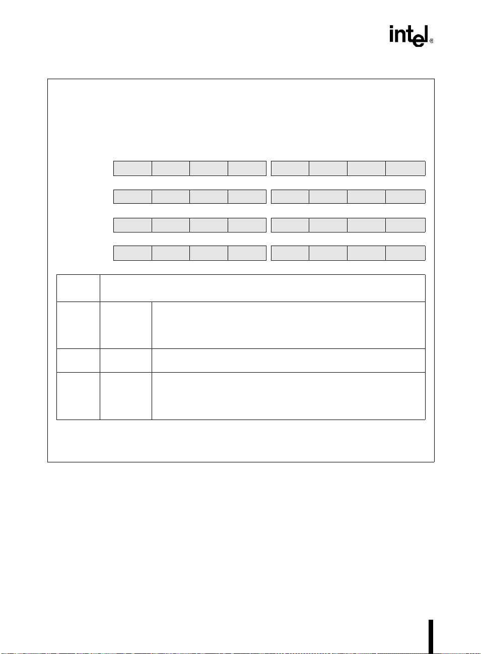
87C196CB SUPPLEMENT
CAN_MSK15
(87C196CB)
Program the CAN message 15 mask (CAN_MSK15) register to mask (“don’t care”) specific mess age
identifier bits for message 15 in addition to those bits masked by a global mask (CAN_EGMSK or
CAN_SGMSK).
87C196CB
Bit
Number
31:27 MSK4:0 ID Mask
26:24 — Reserved. These bits are undefined; for com patibility with f uture devices ,
23:16
15:8
7:0
†
Setting a CAN_MSK15 bit in any position that is cleared in the global mask register has no effect.
The message 15 mask is ANDed with the global mask, so any “don’t care” bits defined in a global
mask are also “don’t care” bits for message 15.
†
31 24
MSK4 MSK3 MSK2 MSK1 MSK0 — — —
23 16
MSK12 MSK11 MSK10 MSK9 MSK8 MSK7 MSK6 MSK5
15 8
MSK20 MSK19 MSK18 MSK17 MSK16 MSK15 MSK14 MSK13
7 0
MSK28 MSK27 MSK26 MSK25 MSK24 MSK23 MSK22 MSK21
These bits individually mask incoming message identifier (ID) bits.
0 = mask the ID bit (accept either “0” or “1”)
1 = accept only an exact match
do not modify these bits.
MSK12:5
MSK20:13
MSK28:21
ID Mask
These bits individually mask incoming message identifier (ID) bits.
0 = mask the ID bit (accept either “0” or “1”)
1 = accept only an exact match
Function
Address:
Reset State:
1E0FH, 1E0EH,
1E0DH, 1E0CH
Unchanged
Figure 7-11. CAN Message 15 Mask (CAN_MSK15) Register
7.5 CONFIGURING MESSAGE OBJECTS
Each message object consists of a configuration register, a message identifier, control registers,
and data registers (from zero to eight bytes of data). This section explains how to configur e message objects and determine their status.
7-20
Page 82

CAN SERIAL COMMUNICATIONS CONTROLLER
7.5.1 Specifying a Message Object’s Configuration
Each message object configuration register (Figure 7-12) specifies a message identifier type
(standard or extended), transfer direction (transmit or receive), and data length (in bytes).
CAN_MSGxCFG
x
= 1–15 (87C196CB)
Program the CAN message object
object’s data length, transfer direction, and identifier type.
7 0
87C196CB
Bit
Number
7:4 DLC3:0 Data Length Code
3 DIR Direction
2 XTD Extended Identifier Used
1:0 — Reserved; for compatibility with future devices, write zeros to these bits.
DLC3 DLC2 DLC1 DLC0 DIR XTD — —
Bit
Mnemonic
x
configuration (CAN_MSGxCFG) register to specify a message
Specify the number of data bytes this message object contains. Valid
values are 0–8. The CAN controller updates a receive message object’s
data length code after each reception to reflect the number of data bytes in
the current message.
Specify whether this message object is to be transmitted or is to receive a
message object from a remote node.
0 = receive
1 = transmit
Specify whether this message object’s identification registers contain an
extended (29-bit) or a standard (11-bit) identifier.
0 = standard identifier
1 = extended identifier
Address:
Reset State:
Function
1E
x
6H (x = 1–F)
Unchanged
Figure 7-12. CAN Message Object x Configuration (CAN_MSGxCFG) Register
Set the XTD bit for a message object with an extended identifier; clear it for a message with a
standard identifier. If you accidentally clear the XTD bit for a m essage that has an extend ed identifier, the CAN controller will clear the extended bits in the identification register. If you set the
XTD bit for a message object, that message object cannot receive message objects with stand ard
identifiers.
For a transmit message, set the DIR bit and write the number of prog rammed data bytes (0–8) to
the DLC field. For a receive message, clear the DIR bit. The CAN controller stor es the data length
from the received message in the DLC field.
7-21
Page 83

87C196CB SUPPLEMENT
7.5.2 Programming the Message Object Identifier
Each message identifier register (Figure 7-13) specifies the message’s identifier. For messages
with extended identifiers, write the identifier to bits ID28:0. For messages with standard identifiers, write the identifier to bits ID28:18. Software can chang e the identifier during normal operation without requiring a subsequent device reset. Clear the MSGVAL bit in the corresponding
message control register 0 to prevent the CAN co ntroller from accessing the message object while
the modification takes place, then set the bit to allow access.
CAN_MSGxID0–3
x
= 1–15 (87C196CB)
Write the message object’s identifier to the CAN message object
register. Software can change the identifier during normal operation. Clear the MSGVAL bit in the
corresponding CAN_MSG
change the identifier in CAN_MSG
87C196CB 31 24
CAN_MSG
CAN_MSG
CAN_MSG
CAN_MSG
Bit
Number
31:27
23:16
12:8
26:24 — Reserved; for compatibility with future devices, write zeros to these bits.
15:13
7:0
†
This register is the same as the arbitration register in the standalone 82527 CAN peripheral.
†
x
CON0 register to prevent the CPU from accessing the message object,
x
ID0–3, then set the MSGVAL bit to allow access.
x
ID3 ID4 ID3 ID2 ID1 ID0 — — —
23 16
x
ID2 ID12 ID11 ID10 ID9 ID 8 ID7 ID6 ID5
15 8
x
ID1 ID20 ID19 ID18 ID17 ID16 ID15 ID14 ID13
7 0
x
ID0 ID28 ID27 ID26 ID25 ID24 ID23 ID22 ID21
Bit
Mnemonic
ID4:0
ID12:5
ID17:13
ID20:18
ID28:21
Message Identifier 17:0
These bits hold the 18 least-significant bits of an extended identifier. If
you write an extended identifier to these bits, but specify a standard
identifier (XTD = 0) in the corresponding message object’s configuration
register (CAN_MSG
Message Identifier 28:18
These bits hold either an entire standard identifier or the 11 most-
significant bits of an extended identifier.
x
CFG), the CPU clears these bits (ID17:0).
Address:
Reset State:
x
identifier (CAN_MSGxID0–3)
Function
1E
1E
(
x
Unchanged
x
5H, 1Ex4H,
x
3H, 1Ex2H
= 1–F)
7-22
Figure 7-13. CAN Message Object x Identifier (CAN_MSGxID0–3) Register
Page 84

CAN SERIAL COMMUNICATIONS CONTROLLER
7.5.3 Programming the Message Object Control Registers
Each message object control register consists of four bit pairs — one bit of each pair is in true
form and one is in complement form. This format allows software to set or clear any bit with a
single write operation, without affecting the remaining bits. Table 7-12 shows how to interpret
the bit-pair values.
Table 7-12. Control Register Bit-pair Interpretation
Access Type MSB LSB Defi nition
0 0 Not allowed (indeterminate)
Write
Read
7.5.3.1 Message Object Control Register 0
0 1 Clear (0)
1 0 Set (1)
1 1 No change
0 1 Clear (0)
1 0 Set (1)
Message object control register 0 (Figure 7-14 ) indicates whether an interrupt is pending, contro ls
whether a successful transmission or reception generates an interrupt, and indicates whether a
message object is ready to transmit.
7.5.3.2 Message Object Control Register 1
Message object control register 1 (Figure 7-15) indicates whether the message object contains
new data, whether a message has been overwritten, whether the message is being updated, and
whether a transmission or reception is pending. Message objects 1–14 have only a single buffer,
so if a second message is received before the CPU reads the first, the first message is overwritten.
Message object 15 has two alternating buffers, so it can receive a second message while the first
is being processed. However, if a third message is received while the CPU is reading the first, the
second message is overwritten.
7.5.4 Programming the Message Object Data
Each message object can have from zero to eight bytes of data. For transmit message objects,
write the message data to the data registers (Figure 7-16). For receiv e message objects, the CAN
controller stores the received data in these registers. The CAN controller writes random value s to
any unused data bytes during operation, so you should not use unused data bytes as scratch-pad
memory.
7-23
Page 85

87C196CB SUPPLEMENT
CAN_MSGxCON0
x
= 1–15 (87C196CB)
x
Program the CAN message object
message object is ready to transmit and to control whether a successful transmiss ion or reception
generates an interrupt. The least-significant bit-pair indicates whether an interrupt is pending.
This register consists of four bit-pairs — the most-significant bit of each pair is in true form and the
least-significant bit is in complement form. This format allows softwar e to set or clear any bit with a
single write operation, without affecting the remaining bits.
7 0
87C196CB
Bit
Number
7:6 MSGVAL Message Object Valid
5:4 TXIE Transmit Interrupt Enable
MSGVAL MSGVAL TXIE TXIE RXIE RXIE INT_PND INT_PND
Bit
Mnemonic
Set this bit-pair to indicate that a message object is valid (configured and
ready for transmission or reception).
bit 7 bit 6
0 1 not ready
1 0 message object is valid
The CAN peripheral will access a message object only if this bit-pair
indicates that the message is valid. If multiple message objects have the
same identifier, only one can be valid at any given time.
During initialization, software should clear this bit for any unused message
objects. Software can clear this bit if a message is no longer needed or if
you need to change a message object’s contents or identifier.
Receive message objects do not use this bit-pair.
For transmit message objects, set this bit-pair to enable the CAN
peripheral to initiate a transmit (TX) interrupt after a successful transmission. You must also set the interrupt enable bit (CAN_CON.1) to enable
the interrupt.
bit 5 bit 4
0 1 no interru pt
1 0 generate an interrupt
control 0 (CAN_MSGxCON0) register to indicate whether the
Address:
Reset State:
Function
1E
x
0H (x = 1–F)
Unchanged
7-24
Figure 7-14. CAN Message Object x Control 0 (CAN_MSGxCON0) Register
Page 86

CAN SERIAL COMMUNICATIONS CONTROLLER
CAN_MSG
x
= 1–15 (87C196CB)
Program the CAN message object
message object is ready to transmit and to control whether a successful transmiss ion or reception
generates an interrupt. The least-significant bit-pair indicates whether an interrupt is pending.
This register consists of four bit-pairs — the most-significant bit of each pair is in true form and the
least-significant bit is in complement form. This format allows softwar e to set or clear any bit with a
single write operation, without affecting the remaining bits.
87C196CB
Number
3:2 RXIE Receive Interrupt Enable
1:0 INT_PND Interrupt Pending
Bit
x
CON0 (Continued)
x
control 0 (CAN_MSGxCON0) register to indicate whether the
7 0
MSGVAL MSGVAL TXIE TXIE RXIE RXIE INT_PND INT_PND
Bit
Mnemonic
Transmit message objects do not use this bit-pair.
For a receive message object, set this bit-pair to enable this message
object to initiate a receive (RX) interrupt after a successful reception. You
must also set the interrupt enable bit (CAN_CON.1) to enable the interrupt.
bit 3 bit 2
0 1 no interru pt
1 0 generate an interrupt
This bit-pair indicates that this message object has initiated a transmit (TX)
or receive (RX) interrupt. Software must clear this bit when it services the
interrupt.
bit 1 bit 0
0 1 no interru pt
1 0 an interru pt was generat ed
Address:
Reset State:
Function
1E
x
0H (x = 1–F)
Unchanged
Figure 7-14. CAN Message Object x Control 0 (CAN_MSGxCON0) Register (Continued)
7-25
Page 87

87C196CB SUPPLEMENT
CAN_MSGxCON1
x
= 1–15 (87C196CB)
The CAN message object
Address:
Reset State:
x
control 1 (CAN_MSGxCON1) register indicates whether a message
1E
x
1H (x = 1–F)
Unchanged
object has been updated, whether a message has been overwritten, whether the CPU is updating the
message, and whether a transmission or reception is pending.
This register consists of four bit-pairs — the most-significant bit of each pair is in true form and the
least-significant bit is in complement form. This format allows software to set or clear any bit with a
single write operation, without affecting the remaining bits.
7 0
87C196CB
Bit
Number
RMTPND RMTPND TX_REQ TX_REQ
Bit
Mnemonic
MSGLST
CPUUPD
Function
MSGLST
CPUUPD
NEWDAT NEWDAT
7:6 RMTPN D Remote Request Pending
Receive message objects do not use this bit-pair.
The CAN controller sets this bit-pair to indicate that a remote frame has
requested the transmission of a transmit message object. If the CPUUPD
bit-pair is clear, the CAN controller transmits the message object, then
clears RMTPND. Setting RMTPND does not cause a transmission; it only
indicates that a transmission is pending.
bit 7 bit 6
0 1 no pending request
1 0 a remote request is pending
5:4 TX_RE Q T ransm ission Request
Set this bit-pair to cause a receive message object to transmit a remote
frame (a request for transmission) or to cause a transmit object to transmit
a data frame. Read this bit-pair to determine whether a transmission is in
progress.
bit 5 bit 4
0 1 no pending request; no transmission in progress
1 0 transm ission request ; transmission in progress
7-26
Figure 7-15. CAN Message Object x Control 1 (CAN_MSGxCON1) Register
Page 88

CAN SERIAL COMMUNICATIONS CONTROLLER
CAN_MSG
x
= 1–15 (87C196CB)
x
CON1 (Continued)
The CAN message object
x
control 1 (CAN_MSGxCON1) register indicates whether a message
Address:
Reset State:
1E
x
1H (x = 1–F)
Unchanged
object has been updated, whether a message has been overwritten, whether the CPU is updating the
message, and whether a transmission or reception is pending.
This register consists of four bit-pairs — the most-significant bit of each pair is in true form and the
least-significant bit is in complement form. This format allows software to set or clear any bit with a
single write operation, without affecting the remaining bits.
7 0
87C196CB
Bit
Number
RMTPND RMTPND TX_REQ TX_REQ
Bit
Mnemonic
3:2 MSGLST or
CPUUPD
MSGLST
CPUUPD
Function
Message Lost (Receive)
For a receive message object, the CAN controller sets this bit-pair to
MSGLST
CPUUPD
NEWDAT NEWDAT
indicate that it stored a new message while the NEWDAT bit-pair was still
set, overwriting the previous message.
bit 3 bit 2
0 1 no overwrite occurr ed
1 0 a message was lost (overwritt en)
CPU Updating (Transmit)
For a transmit message object, software should set this bit-pair to indicate
that it is in the process of updating the message contents. This prevents a
remote frame from triggering a transmission that would contain invalid
data.
bit 3 bit 2
0 1 the message is valid
1 0 software is updating data
1:0 NEWDA T New Data
This bit-pair indicates whether a message object is valid (configured and
ready for transmission).
bit 1 bit 2
0 1 not ready
1 0 message object is valid
For receive message objects, the CAN peripheral sets this bit-pair when it
stores new data into the message object.
For transmit message objects, set this bit-pair and clear the CPUUPD bitpair to indicate that the message contents have been updated. Clearing
CPUUPD prevents a remote frame from triggering a transmission that
would contain invalid data.
During initialization, clear this bit for any unused message objects.
Figure 7-15. CAN Message Object x Control 1 (CAN_MSGxCON1) Register (Continued)
7-27
Page 89

87C196CB SUPPLEMENT
CAN_MSGxDATA0–7
x
= 1–15 (87C196CB)
The CAN message object data (CAN_MSG
received. Any unused data bytes have random values that change during operation.
87C196CB 7 0
x
CAN_MSG
CAN_MSG
CAN_MSG
CAN_MSG
CAN_MSG
CAN_MSG
CAN_MSG
CAN_MSG
DATA7 Data 7
7 0
x
DATA6 Data 6
7 0
x
DATA5 Data 5
7 0
x
DATA4 Data 4
7 0
x
DATA3 Data 3
7 0
x
DATA2 Data 2
7 0
x
DATA1 Data 1
7 0
x
DATA0 Data 0
x
DATA0–7) registers contain data to be transmitted or data
Address:
Reset State:
1E
x
EH, 1ExDH,
1E
x
CH, 1ExBH,
1E
x
AH, 1Ex9H,
1E
x
8H, 1Ex7H
(
x
= 1–F)
Unchanged
Bit
Number
7:0 Data
Figure 7-16. CAN Message Object Data (CAN_MSGxDATA0–7) Registers
7-28
Function
Each message object can use from zero to eight data registers to hold data to
be transmitted or data received.
For receive message objects, these registers accept data during a reception.
For transmit message objects, write the data that is to be transmitted to these
registers. The number of data bytes must match the DLC field in the
CAN_MSG
CAN_MSG1DATA1, CAN_MSG1DATA2, and CAN_MSG1DATA3 contain data,
the DLC field in CAN_MSG1CFG must contain 04H.)
x
CFG register. (For example, if CAN_MSG 1DAT A 0,
Page 90

CAN SERIAL COMMUNICATIONS CONTROLLER
7.6 ENABLING THE CAN INTERRUPTS
The CAN controller has a single interrupt input (INT13) to the interrupt controller. (Generally,
PTS interrupt service is not useful for the CAN controller because the PTS cannot readily determine the source of the CAN controller’s mu ltiplexed interr upts.) To enab le the CAN co ntroller’s
interrupts, you must enable the interrupt source by setting the CAN bit in INT_MASK1 (see Table 7-2 on page 7-3) and globally enable interrupt servicing (by executing the EI instruction). In
addition, you must set bits in the CAN control register (Figure 7-17) and the individual message
objects’ control register 0 (Figu re 7-18) to enable th e individual interrup t sources within the CAN
controller.
CAN_CON
(87C196CB)
Program the CAN control (CAN_CON) register to control write access to the bit timing registers, to
enable and disable CAN interrupts, and to control access to the CAN bus.
7 0
87C196CB
Bit
Number
7 — Reserved; for compatibility with future devices, write zero to this bit.
6 CCE Change Configuration Enable
5:4 — Reserved; for compatibility with future devices, write zeros to these bits.
3 EIE Error Interrupt Enable
2 SIE Status-ch ange Interrupt Enable
— CCE — — EIE SIE IE INIT
Bit
Mnemonic
This bit enables and disables the bus-off and warn interrupts.
0 = disable bus-off and warn interrupts
1 = enable bus-off and warn interrupts
This bit enables and disables the successful reception (RXOK), successful
transmission (TXOK), and error code change (LEC2:0) interrupts.
0 = disable status-change interrupt
1 = enable status-change interrupt
When the SIE bit is set, the CAN controller generates a successful
reception (RXOK) interrupt request each time it receives a valid message,
even if no message object accepts it.
Function
Address:
Reset State:
1E00H
01H
Figure 7-17. CAN Control (CAN_CON) Register
7-29
Page 91

87C196CB SUPPLEMENT
CAN_CON (Continued)
(87C196CB)
Program the CAN control (CAN_CON) register to control write access to the bit timing registers, to
enable and disable CAN interrupts, and to control access to the CAN bus.
7 0
87C196CB
Bit
Number
1 IE Interrupt Enable
0 INIT Software Initialization Enable
— CCE — — EIE SIE IE INIT
Bit
Mnemonic
This bit globally enables and disables interrupts (error, status-change, and
message object transmit and receive interrupts).
0 = disable interrupts
1 = enable interrupts
When the IE bit is set, an interrupt is generated only if the corresponding
interrupt source’s enable bit (EIE or SIE in CAN_CON; TXIE or RXIE in
CAN_MSG
updates the CAN interrupt pending register, but does not generate an
interrupt.
x
_CON0) is also set. If the IE bit is clear, an interrupt request
Function
Address:
Reset State:
1E00H
Figure 7-17. CAN Control (CAN_CON) Register (Continued)
01H
7-30
Page 92

CAN SERIAL COMMUNICATIONS CONTROLLER
CAN_MSGxCON0
x
= 1–15 (87C196CB)
x
Program the CAN message object
message object is ready to transmit and to control whether a successful transmiss ion or reception
generates an interrupt. The least-significant bit-pair indicates whether an interrupt is pending.
This register consists of four bit-pairs — the most-significant bit of each pair is in true form and the
least-significant bit is in complement form. This format allows softwar e to set or clear any bit with a
single write operation, without affecting the remaining bits.
7 0
87C196CB
Bit
Number
7:6 MSGVAL Message Object Valid
5:4 TXIE Transmit Interrupt Enable
3:2 RXIE Receive Interrupt Enable
1:0 INT_PND Interrupt Pending
MSGVAL MSGVAL TXIE TXIE RXIE RXIE INT_PND INT_PND
Bit
Mnemonic
Receive message objects do not use this bit-pair.
For transmit message objects, set this bit-pair to enable the CAN
peripheral to initiate a transmit (TX) interrupt after a successful transmission. You must also set the interrupt enable bit (CAN_CON.1) to enable
the interrupt.
bit 5 bit 4
0 1 no interru pt
1 0 generate an interrupt
Transmit message objects do not use this bit-pair.
For receive message objects, set this bit-pair to enable the CAN peripheral
to initiate a receive (RX) interrupt after a successful reception. You must
also set the interrupt enable bit (CAN_CON.1) to enable the interrupt.
bit 3 bit 2
0 1 no interru pt
1 0 generate an interrupt
control 0 (CAN_MSGxCON0) register to indicate whether the
Address:
Reset State:
Function
1E
x
0H (x = 1–F)
Unchanged
Figure 7-18. CAN Message Object x Control 0 (CAN_MSGxCON0) Register
When the SIE bit in the CAN control register is set, the CAN controller generates a successful
reception (RXOK) interrupt request each time it receives a valid message, even if no message object accepts it. If you set both the SIE bit (Figure 7-17) and an individual message object’s RXIE
bit (Figure 7-18), the CAN controller gen erates two interrupt requests each time a message object
receives a message. The status change interrupt is useful during developmen t to detect bu s error s
caused by noise or other hardware problems. However, you should disable this interrupt during
normal operation in most applications. If the status change interrupt is enabled, each status
change generates an interrupt request, placing an unnecessary burden on the CPU. To prevent redundant interrupt req uests, enable the er ror interrupt sou rces (with th e EIE bit) and enab le the receive and transmit interrupts in the individual message objects.
7-31
Page 93

87C196CB SUPPLEMENT
7.7 DETERMINING THE CAN CONTROLLER’S INTERRUPT STATUS
A successful reception or transmission or a change in the status register can cause the CAN controller to generate an interrupt r equest. Th e INT_PEND1 r egister (see Table 7 -2 on p age 7 -3) indicates whether a CAN interrupt request is pending. The CAN interrupt pending reg i ster (Fig ure
7-19) indicates the source of the request (either the status register or a specific message object).
Your interrupt service routine should read the CAN_INT register to ensure that no additional interrupts are pending before executing the return instruction.
CAN_INT
read-only (87C196CB)
The CAN interrupt pending (CAN_INT) register indicates the source of the highest priority pending
interrupt. If a status change generated the interrupt request, software can read the status register
(CAN_STAT) to determine whether the interrupt request was caused by an abnormal error rate, a
successful reception, a successful transmis sion, or a new error. If an individual message object
generated the interrupt request, software can read the associated message object control 0 register
(CAN_MSG
request is pending.
87C196CB
Number
7:0 Pending Interrupt
Bit
x
CON0). The INT_PND bit-pair will be set, indicating that a receive or transmit interrupt
7 0
Pending Interrupt
Function
This field indicates the source of the highest priority pending interrupt.
Value Pen di ng Interru p t Priori ty (15 is hi ghest; 0 is low est)
00H none —
01H stat us regist er 15
02H message object 15 14
03H message object 1 13
04H message object 2 12
05H message object 3 11
06H message object 4 10
07H message object 5 9
08H message object 6 8
09H message object 7 7
0AH message object 8 6
0BH message object 9 5
0CH message object 10 4
0DH message object 11 3
0EH message object 12 2
0FH message object 13 1
10H message object 14 0
Address:
Reset State:
1E5FH
00H
Figure 7-19. CAN Interrupt Pending (CAN_INT) Register
If a status change generated the interrupt (CAN_INT = 01H), software can read the CAN status
register (Figure 7-20) to determine the source of the interrupt request.
7-32
Page 94

CAN SERIAL COMMUNICATIONS CONTROLLER
CAN_STAT
(87C196CB)
The CAN status (CAN_STAT) register reflects the current stat us of the CAN peripheral.
7 0
87C196CB
Bit
Number
7 BUSOFF Bus-off Status
6 WARN Warning Status
5 — Reserved. This bit is undefined.
4 RXOK Reception Successful
3 TXOK Transmission Successful
2:0 LEC2:0 Last Error Code
BUSOFF WARN — RXOK TXOK LEC2 LEC1 LEC0
Bit
Mnemonic
The CAN peripheral sets this read-only bit to indicate that it has isolated
itself from the CAN bus (floated the TX pin) because an error counter has
reached 256. A bus-off recovery sequence clears this bit and clears the
error counters. (See “Bus-off State” on page 7-41.)
The CAN peripheral sets this read-only bit to indicate that an error counter
has reached 96, indicating an abnormal rate of errors on the CAN bus.
The CAN peripheral sets this bit to indicate that a message has been
successfully received (error free, regardless of acknowledgment) since the
bit was last cleared. Software must clear this bit when it services the
interrupt.
The CAN peripheral sets this bit to indicate that a message has been
successfully transmitted (error free and acknowledged by at least one
other node) since the bit was last cleared. Software must clear this bit
when it services the interrupt.
This field indicates the error type of the first error that occurs in a message
frame on the CAN bus. (“Error Detection and Management Logic” on page
7-9 describes the error types.)
LEC2 LEC1 LEC0 Error Type
0 0 0 no error
001stuff error
0 1 0 form error
0 1 1 acknowledgment error
1 0 0 bit 1 error
1 0 1 bit 0 error
1 1 0 CRC error
1 1 1 unused
Function
Address:
Reset State:
1E01H
XXH
Figure 7-20. CAN Status (CAN_STAT) Register
If an individual message object caused the interrupt request (CAN_INT = 02–10H), software can
read the associated message object control 0 register (Figure 7-21). The INT_PND bit-pair will
be set, indicating that a receive or transmit interrupt request is pending
7-33
Page 95

87C196CB SUPPLEMENT
.
CAN_MSGxCON0
(
n
= 1–15)
Program the CAN message object
Address: 1E
Reset State: Unchanged
x
control 0 register (CAN_MSGxCON0) to indicate whether the
x
0H (x=1–F)
message object is ready to transmit and to control whether a successful transmission or reception
generates an interrupt. The most-significant bit-pair indicates whether an interrupt is pending.
This register consists of four bit-pairs — the most-significant bit of each pair is in true form and the
least-significant bit is in complement form. This format allows software to set or clear any bit with a
single write operation, without affecting the remaining bits.
7 0
MSGVAL MSGVA L TXIE TXIE RXIE RXIE INT_PN D INT_PND
Bit
Number
Bit
Mnemonic
Function
7:6 MSGVAL Message Object Valid
5:4 TXIE Transmit Interrupt Enable
3:2 RXIE Receive Interrupt Enable
1:0 INT_PND Interrupt Pending
This bit-pair indicates that the CAN peripheral has initiated a transmit (TX)
or receive (RX) interrupt. Software must clear this bit when it services the
interrupt.
01 = no interrupt
10 = an interrupt was generated
Figure 7-21. CAN Message Object x Control 0 (CAN_MSGxCON0) Register
7-34
Page 96

CAN SERIAL COMMUNICATIONS CONTROLLER
7.8 FLOW DIAGRAMS
The flow diagrams in this section describe the steps that your software (shown as CPU) and the
CAN controller execute to receive and transmit messages. Table 7-13 lists the reg ister bits shown
in the diagrams along with their associated registers and a cross-reference to the figure that describes them.
Table 7-13. Cross-reference for Register Bits Shown in Flowcharts
Bit Mnemonic Register Mnemonic Figure and Page
CPUUPD CAN_MSG
DIR CAN_MSG
DLC CAN_MSG
ID CAN_MSG
INT_PND CAN_MSG
MSGLST CAN_MSG
MSGVAL CAN_MSG
NEWDAT CAN_MSG
RMTPND CAN_MSG
RXIE CAN_MSG
TXIE CAN_MSGxCON0 Figure 7-14 on page 7-24
TX_REG CAN_MSG
XTD CAN_MSG
x
CON1 Figure 7-15 on page 7-26
x
CFG Figure 7-12 on page 7-21
x
CFG Figure 7-12 on page 7-21
x
ID Figure 7-13 on page 7-22
x
CON0 Figure 7-14 on page 7-24
x
CON1 Figure 7-15 on page 7-26
x
CON0 Figure 7-14 on page 7-24
x
CON1 Figure 7-15 on page 7-26
x
CON1 Figure 7-15 on page 7-26
x
CON0 Figure 7-14 on page 7-24
x
CON1 Figure 7-15 on page 7-26
x
CFG Figure 7-12 on page 7-21
7-35
Page 97

87C196CB SUPPLEMENT
Power Up
Initialization
Process
(All bits undefined)
MSGVAL
INT_PND
TXIE
RXIE
NEWDAT
RMTPND
TX_REQ
MSGLST
DLC
DIR
XTD
ID
:= 1
:= 0
:= (Application specific)
:= (Application specific)
:= 0
:= 0
:= 0
:= 0
:= (don't care)
:= 0 (receive)
:= (Application specific)
:= (Application specific)
NEWDAT := 0
Process message contents.
NEWDAT = 1?
Yes
Restart Process
7-36
No
No
Request update?
Yes
TX_REQ := 1
Figure 7-22. Receiving a Message for Message Objects 1–14 — CPU Flow
A2594-01
Page 98

CAN SERIAL COMMUNICATIONS CONTROLLER
Power Up
Initialization
Process
(All bits undefined)
MSGVAL
INT_PND
RXIE
NEWDAT
RMTPND
MSGLST
DIR
XTD
ID
MASK
:= 1
:= 0
:= (Application specific)
:= 0
:= 0
:= 0
:= 0 (receive)
:= (Application specific)
:= (Application specific)
:= (Application specific)
Process message contents.
INT_PND := 0
NEWDAT := 0 and RMTPND := 0
NEWDAT = 1?
Yes
Restart Process
No
Figure 7-23. Receiving a Message for Message Object 15 — CPU Flow
A2597-02
7-37
Page 99

87C196CB SUPPLEMENT
No
TX_REQ=1?
MSGLST=0?
NEWDAT := 0
Load identifer and
control into buffer
Send remote frame
No
Transmission
successful?
TX_REQ := 0
RMTPND:= 0
Yes
Yes
Yes
Bus idle?
MSGLST := 1
No
Received frame with
same identifer as this
message object?
NEWDAT = 1?
Store message
NEWDAT := 1
TX_REQ := 0
RMTPND := 0
RXIE = 1?
No
Yes
No
7-38
No
TXIE = 1?
Yes
INT_PND := 1
INT_PND := 1
Figure 7-24. Receiving a Message — CAN Controller Flow
Yes
A2598-01
Page 100

CAN SERIAL COMMUNICATIONS CONTROLLER
Power Up
Initialization
Update
(All bits undefined)
MSGVAL
INT_PND
TXIE
RXIE
NEWDAT
RMTPND
TX_REQ
MSGLST
DLC
DIR
XTD
ID := (Application specific)
Write/calculate message contents.
:= 1
:= 0
:= (Application specific)
:= (Application specific)
:= 0
:= 0
:= 0
:= 0
:= (Application specific)
:= 1 (transmit)
:= (Application specific)
CPUUPD := 1
NEWDAT := 1
CPUUPD := 0
Yes
TX_REQ := 1
Want to send?
No
Update message?
Yes
Figure 7-25. Transmitting a Message — CPU Flow
A2596-01
7-39
 Loading...