

Page 1

8XC196Lx Supplement to
8XC196Kx, 8XC196Jx,
87C196CA User’s Manual
August 2004
Order Number: 272973-003
Page 2

Information in this document is provided in connection with Intel products. No license, express or implied, by estoppel or
herwise, to any intellectual property rights is granted by this document. Except as provided in Intel’s Terms and Conditions
ot
of Sale for such products, Intel assumes no liability whatsoever, and Intel disclaims any express or implied warranty, relating
to sale and/or use of Intel products including liability or warranties relating to fitness for a particular purpose, merchantability,
or infringement of any patent, copyright or other intellectual property right. Intel products are not intended for use in medical,
e saving, or life sustaining applications.
lif
In
tel may make changes to specifications and product descriptions at any time, without notice.
Designers must not rely on the absence or characteristics of any features or instructions marked "reserved" or "undefined."
Intel reserves these for future definition and shall have no responsibility whatsoever for conflicts or incompatibilities arising
om future changes to them.
fr
The 8XC196Lx, 8XC196Kx, 8XC196Jx and 87C196CA microprocessors may contain design defects or errors known as
errata which may cause the products to deviate from published specifications. Current characterized errata are available on
request.
Contact your local Intel sales office or your distributor to obtain the latest specifications and before placing your product order.
Copies of documents which have an ordering number and are referenced in this document, or other Intel literature may be
obtained by calling 1-800-548-4725 or by visiting Intel’s website at http://www.intel.com.
Copyright © Intel Corporation, 2004
*Third-party brands and names are the property of their respective owners.
Page 3

CONTENTS
CHAPTER 1
GUIDE TO THIS MANUAL
1.1 MANUAL CONTENTS................................................................................................... 1-1
1.2 RELATED DOCUMENTS.............................................................................................. 1-2
CHAPTER 2
ARCHITECTURAL OVERVIEW
2.1 MICROCONTROLLER FEATURES.............................................................................. 2-1
2.2 BLOCK DIAGRAM............................................ ...... ....................................................... 2-2
2.3 INTERNAL TIMING........................................................................................................ 2-2
2.4 EXTERNAL TIMING...................................................................................................... 2-5
2.5 INTERNAL PERIPHERALS........................................................................................... 2-6
2.5.1 I/O Ports ........................................... ...... ..... ...... ..... ............................................... ....2-7
2.5.2 Synchronous Serial I/O Port .....................................................................................2-7
2.5.3 Event Processor Array ..............................................................................................2-7
2.5.4 J1850 Communications Controller ............................................................................2-7
2.6 DESIGN CONSIDERATIONS........................................................................................ 2-7
CHAPTER 3
ADDRESS SPACE
3.1 ADDRESS PARTITIONS............................................................................................... 3-1
3.2 REGISTER FILE.................................... ...... .................................................................. 3-2
3.3 PERIPHERAL SPECIAL-FUNCTION REGISTERS...................................................... 3-4
3.4 WINDOWING................................................................................................................. 3-6
CHAPTER 4
STANDARD AND PTS INTERRUPTS
4.1 INTERRUPT SOURCES, VECTORS, AND PRIORITIES............................................. 4-1
4.2 INTERRUPT REGISTERS............................................................................................. 4-2
4.2.1 Interrupt Mask Registers ............................................................... ............................4-3
4.2.2 Interrupt Pending Registers ........................ ...... ..... ............................................. ......4-4
4.2.3 Peripheral Transaction Server Registers ..................................................................4-6
CHAPTER 5
I/O PORTS
5.1 I/O PORTS OVERVIEW................................................................................................ 5-1
5.2 INTERNAL STRUCTURE FOR PORTS 1, 2, 5, AND 6 (BIDIRECTIONAL PORTS).... 5-1
5.2.1 Configuring Ports 1, 2, 5, and 6 (Bidirectional Ports) ................................................5-3
5.2.2 Special Bidirectional Port Considerations .................................................................5-4
5.3 INTERNAL STRUCTURE FOR PORTS 3 AND 4 (ADDRESS/DATA BUS).................. 5-5
iii
Page 4

8XC196LX SUPPLEMENT
CHAPTER 6
SYNCHRONOUS SERIAL I/O PORT
6.1 SSIO 0 CLOCK REGISTER........................................................................................... 6-1
6.2 SSIO 1 CLOCK REGISTER........................................................................................... 6-2
CHAPTER 7
EVENT PROCESSOR ARRAY
7.1 EPA FUNCTIONAL OVERVIEW................................................................................... 7-1
7.1.1 EPA Mask Registers .................. ............................................. ...... ..... ...... ...... ...........7-4
7.1.2 EPA Pending Registers .......................................................... ...... ..... ...... .................7-5
7.1.3 EPA Interrupt Priority Vector Register .......................................................................7-6
CHAPTER 8
J1850 COMMUNICATIONS CONTROLLER
8.1 J1850 FUNCTIONAL OVERVIEW................................................................................. 8-1
8.2 J1850 CONTROLLER SIGNALS AND REGISTERS..................................................... 8-3
8.3 J1850 CONTROLLER OPERATION............................................................................. 8-4
8.3.1 Control State Machine ..............................................................................................8-4
8.3.1.1 Cyclic Redundancy Check Generator ..................................................................8-4
8.3.1.2 Bus Contention .....................................................................................................8-5
8.3.1.3 Bit Arbitration ........................................................................................................8-5
8.3.1.4 Error Detection .....................................................................................................8-5
8.3.2 Symbol Synchronization and Timing Circuitry ...........................................................8-5
8.3.2.1 Clock Prescaler ....................................................................................................8-6
8.3.2.2 Digital Filter ..........................................................................................................8-6
8.3.2.3 Delay Compensation ............................................................................................8-6
8.3.2.4 Symbol Encoding and Decoding ..........................................................................8-6
8.3.3 Bit Arbitration Example .............................................................................................8-7
8.4 MESSAGE FRAMES..................................................................................................... 8-8
8.4.1 Standard Messaging .............................................. ...... ...... ..... ..................................8-9
8.4.1.1 Header .................................................................................................................8-9
8.4.1.2 CRC Byte .............................................................................................................8-9
8.4.1.3 Normalization Bit ..................................................................................................8-9
8.4.1.4 Start and End Message Frame Symbols ............................................................8-10
8.4.2 In-frame Response Messagi ng .................................... ...... ..... ...... ..... ...... ...............8-12
8.4.2.1 IFR Messaging Type 1: Single Byte, Single Responder ....................................8-12
8.4.2.2 IFR Messaging Type 2: Single Byte, Multiple Responders ................................8-12
8.4.2.3 IFR Messaging Type 3: Multiple Bytes, Single Responder ................................8-13
8.5 TRANSMITTING AND RECEIVING MESSAGES....................................................... 8-13
8.5.1 Transmitting Messages ...........................................................................................8-13
8.5.2 Receiving Messages .............................................. ...... ...... ..... ................................8-15
8.5.3 IFR Messages .........................................................................................................8-16
iv
Page 5

CONTENTS
8.6 PROGRAMMING THE J1850 CONTROLLER ............................................................ 8-16
8.6.1 Programming the J1850 Command (J_CMD) Register ..........................................8-16
8.6.2 Programming the J1850 Configuration (J_CFG) Register ......................................8-18
8.6.3 Programming the J1850 Delay Compensation (J_DLY) Register ...........................8-19
8.6.4 Programming the J1850 Status (J_STAT) Register ................................................8-21
CHAPTER 9
MINIMUM HARDWARE CONSIDERATIONS
9.1 IDENTIFYING THE RESET SOURCE........................................................................... 9-1
9.2 DESIGN CONSIDERATIONS FOR 8XC196LA, LB, AND LD....................................... 9-2
CHAPTER 10
SPECIAL OPERATING MODES
10.1 INTERNAL TIMING...................................................................................................... 10-1
10.2 ENTERING AND EXITING ONCE MODE................................................................... 10-2
CHAPTER 11
PROGRAMMING THE NONVOLATILE MEMORY
11.1 SIGNATURE WORD AND PROGRAMMING VOLTAGE VALUES............................. 11-1
11.2 OTPROM ADDRESS MAP.......................................................................................... 11-1
11.3 SLAVE PROGRAMMING CIRCUIT AND ADDRESS MAP......................................... 11-2
11.4 SERIAL PORT PROGRAMMING CIRCUIT AND ADDRESS MAP............................. 11-4
APPENDIX A
SIGNAL DESCRIPTIONS
A.1 FUNCTIONAL GROUPINGS OF SIGNALS ................................................................. A-1
A.2 DEFAULT CONDITIONS.............................................................................................. A-7
GLOSSARY
v
Page 6

8XC196LX SUPPLEMENT
FIGURES
Figure Page
2-1 8XC196L
2-2 Clock Circuitry (87C196LA, LB Only)...........................................................................2-3
2-3 Internal Clock Phases (Assumes PLL is Bypassed).....................................................2-4
2-4 Effect of Clock Mode on Internal CLKOUT Frequency.................................................2-5
2-5 Unerasable PROM 1 (USFR1) Register (LA, LB Only)................................................2-6
3-1 Register File Address Map.................................................... ..... ...... ............................3-3
4-1 Interrupt Mask (INT_MASK) Register......................................... ...... ............................4-3
4-2 Interrupt Mask 1 (INT_MASK1) Register......................................................................4-4
4-3 Interrupt Pending (INT_PEND) Register ......................................................................4-5
4-4 Interrupt Pending 1 (INT_PEND1) Register .................................................................4-6
4-5 PTS Select (PTSSEL) Register....................................................................................4-7
4-6 PTS Service (PTSSRV) Register.................................................................................4-8
5-1 Ports 1, 2, 5, and 6 Internal Structure (87C196LA, LB Only).......................................5-3
5-2 Ports 3 and 4 Internal Structure (87C196LA, LB Only)................................................5-6
6-1 SSIO 0 Clock (SSIO0_CLK) Register...........................................................................6-1
6-2 SSIO 1 Clock (SSIO1_CLK) Register...........................................................................6-2
7-1 EPA Block Diagram (87C196LA, LB Only)...................................................................7-2
7-2 EPA Block Diagram (83C196LD Only)................................................................... ......7-3
7-3 EPA Interrupt Mask (EPA_MASK) Register.................................................................7-4
7-4 EPA Interrupt Mask 1 (EPA_MASK1) Register............................................................7-4
7-5 EPA Interrupt Pending (EPA_PEND) Register.............................................................7-5
7-6 EPA Interrupt Pending 1 (EPA_PEND1) Register........................................................7-5
7-7 EPA Interrupt Priority Vector Register (EPAIPV)..........................................................7-6
8-1 Integrated J1850 Communications Protocol Solution...................................................8-1
8-2 J1850 Communications Controller Block Diagram.......................................................8-2
8-3 Huntzicker Symbol Definition for J1850........................................................................8-7
8-4 Typical VPW Waveform................................................................................................8-7
8-5 Bit Arbitration Example.................................................................................................8-8
8-6 J1850 Message Frames...............................................................................................8-9
8-7 Huntzicker Symbol Definition for the Normalization Bit..............................................8-10
8-8 Definition for Start and End of Frame Symbols..........................................................8-11
8-9 IFR Type 1 Message Frame.......................................................................................8-12
8-10 IFR Type 2 Message Frame.......................................................................................8-13
8-11 IFR Type 3 Message Frame.......................................................................................8-13
8-13 J1850 Transmit Message Structure............................................................................8-14
8-12 J1850 Transmitter (J_TX) Register............................................................................8-14
8-15 J1850 Receive Message Structure.............................................................................8-15
8-14 J1850 Receiver (J_RX) Register................................................................................8-15
8-16 J1850 Command (J_CMD) Register..........................................................................8-17
8-17 J1850 Configuration (J_CFG) Register......................................................................8-18
8-18 J1850 Delay (J_DLY) Register...................................................................................8-20
8-19 J1850 Status (J_STAT) Register................................................................................8-21
9-1 Reset Source (RSTSRC) Register...............................................................................9-1
10-1 Clock Circuitry (87C196LA, LB Only).........................................................................10-2
x
Block Diagram............................................................................................2-2
vi
Page 7

CONTENTS
FIGURES
Figure Page
11-1 Slave Programming Circuit.........................................................................................11-3
11-2 Serial Port Programming Circuit.................................................................................11-4
A-1 87C196LA 52-pin PLCC Package............................. ...... ...... ..... .................................A-3
A-2 87C196LB 52-pin PLCC Package............................. ...... ...... ..... .................................A-5
A-3 83C196LD 52-pin PLCC Package...............................................................................A-7
vii
Page 8

8XC196LX SUPPLEMENT
TABLES
Table Page
1-1 Related Documents......................................................................................................1-2
2-1 Features of the 8XC196Lx and 8XC196Kx Product Famiies................................. ......2-1
2-2 State Times at Various Frequencies.................... ..... ...... ...... .......................................2-4
2-3 Relationships Between Input Frequency, Clock Multiplier, and State Times...............2-5
2-4 UPROM Programming Values and Locations..............................................................2-6
3-1 Address Map................................................................................................................3-1
3-2 Register File Memory Addresses .................................................................................3-3
x
3-3 8XC196L
3-4 Windows.......................................................................................................................3-6
4-1 Interrupt Sources, Vectors, and Priorities........................ ...... ..... ...... ..... .......................4-2
5-1 Microcontroller Ports.....................................................................................................5-1
7-1 EPA Channels........................................................... ...... ...... ..... ...... ............................7-1
7-2 EPA Interrupt Priority Vectors.......................................................................................7-6
8-1 J1850 Controller Signals..............................................................................................8-3
8-2 Control and Status Registers.......................................................................................8-3
8-3 Relationships Between Input Frequency, PLL, and Prescaler Bits..............................8-6
8-4 Huntzicker Symbol Timing Characteristics.................................................................8-11
11-1 Signature Word and Programming Voltage Values....................................................11-1
11-2 87C196LA, LB
11-3 Slave Programming Mode Address Map....................................................................11-3
11-4 Serial Port Programming Mode Address Map............................................................11-5
A-1 87C196LA Signals Arranged by Functional Categories..............................................A-2
A-2 87C196LB Signals Arranged by Functional Categories..............................................A-4
A-3 83C196LD Signals Arranged by Functional Categories..............................................A-6
A-4 Definition of Status Symbols .......................................................................................A-7
A-5 87C196LA, LB Default Signal Conditions....................................................................A-8
A-6 83C196LD Default Signal Conditions..........................................................................A-9
Peripheral SFRs.........................................................................................3-4
OTPROM Address Map.....................................................................11-2
viii
Page 9

Guide to This Manual
1
Page 10

Page 11

CHAPTER 1
GUIDE TO THIS MANUAL
This document is a supplement to the 8XC196Kx, 8XC196Jx, 87C196 CA Microcontr oller Fa mily
User’s Manual. It describes the dif ferences between the 8XC196L x and the 8XC196 Kx family of
microcontrollers. For information not found in this su pplement, please consult the 8XC196Kx,
8XC196Jx, 87C196CA Microcontroller Family User’s Manual (order number 272258) or the
8XC196Lx datasheets listed in the “Related Documents” section of this chapter.
1.1 MANUAL CONTENTS
This supplement contains several chapters, an appendix, a glossary, and an index. This chapter,
Chapter 1, provides an overview of the supplement. This section summarizes the contents of the
remaining chapters and appendixes. The remainder of this chapter provides references to related
documentation.
Chapter 2 — Architectural Overview — compares the features of the 8XC196Lx microcontroller family with those of the 8XC196Kx microcontroller family and describes the 87C196LA,
LB internal clock circuitry.
Chapter 3 — Address Space — describes the addressable memory space of the 52-pin
8XC196Lx, lists the peripheral special-function registers (SFRs), and provides tables of WSR
values for windowing higher memory into the lower register file for direct access.
Chapter 4 — Standard and PTS Interrupts — describes the additional interrupts for the
87C196LB’s J1850 communications controller peripheral and the SFRs that support those interrupts.
Chapter 5 — I/O Ports — describes the port differences and explains the change in the port reset
state from a “logic 1” to a “logic 0” on the 87C196LA, LB.
Chapter 6 — Synchronous Serial I/O Port — describes the enhanced synchronous serial I/O
(SSIO) port and explains how to program the two additional peripheral SFRs.
Chapter 7 — Event Processor Array — describes the event processor array channel differences.
Chapter 8 — J1850 Communications Controller — describes the 87C196LB’s integrated
J1850 controller and explains how to configure it.
Chapter 9 — Minimum Hardware Considerations — describes device reset options through
the reset source register, and discusses hardware design considerations.
Chapter 10 — Special Operating Modes — illustrates the internal clock control circuitry of the
87C196LA, LB and describes how to enter and exit on-circuit emulation (ONCE) mode.
Chapter 11 — Pr ogramming the Nonvolat ile Memory — describes the memory maps and rec-
ommended circuits to support programming of the 87C196LA, LB’s 24 Kbytes of OTPROM.
1-1
Page 12
8XC196LX SUPPLEMENT
Appendix A — Signal Descriptions — provides reference information for the 8XC196Lx de-
vice pins, including description s of the pin functi ons, reset stat us of the I/O and contr ol pins, and
package pin assignments.
Glossary — defines terms with special meaning used throughout this supplement.
Index — lists key topics with page number references.
1.2 RELATED DOCUMENTS
T ab le 1-1 lists additional documen ts that yo u may fi nd usefu l in des igning syst ems inco rporat ing
the 8XC196Lx microcontrollers.
Table 1-1. Related Documents
Title and Description Order Number
8XC196Kx, 8XC196Jx, 87C196CA Microcontroller Family User’s Manual
87C196LA-20 MHz CHMOS 16-Bit Microcontroller Automotive
87C196LB-20 MHz CHMOS 16-Bit Microcontroller Automotive
83C196LD CHMOS 16-Bit Microcontroller Automotive
datasheet 272806
datasheet 272807
datasheet 272805
272258
1-2
Page 13

Architectural
Overview
2
Page 14

Page 15
CHAPTER 2
ARCHITECTURAL OVERVIEW
This chapter describes architectural differences between the 8XC196L x (87C196LA, 87C1 96LB,
and 83C196LD) and the 8XC196Kx (8XC196Kx, 8XC196Jx, and 87C196CA) microcontroller
families. Both the 8XC196Lx and the 8XC196Kx are designed for high-speed calculations and
fast I/O, and share a common architecture and instruction set with few deviations. This chapter
provides a high-level overview of the deviations between th e two families.
NOTE
This supplement describes two product families within the MCS® 96
microcontroller family. For brevity, the name 8XC196Lx is used when the
discussion applies to all three Lx controllers. Likewise, the name 8XC196Kx is
used when the discussion applies to all the Kx, Jx, and CA controllers.
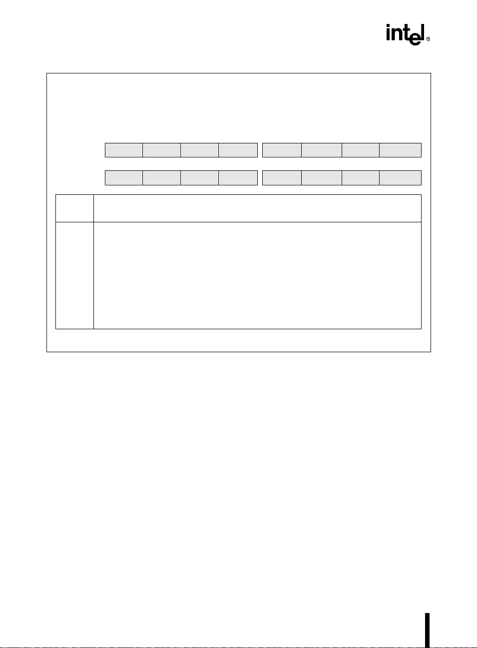
2.1 MICROCONTROLLER FEATURES
Table 2-1 lists the features of the 8XC196Lx and the 8XC196K x.
Table 2-1. Features of the 8XC196Lx and 8XC196Kx Product Famiies
Device Pins
87C196LA 52 24 K 768 —416 3 6— — 1
87C196LB 52 24 K 768 — 41 6 3 6 — 1 1
83C196LD 52 16 K 384 — 41 6 3 — — — 1
8XC196JV 52 48 K 1536 512 41 6 3 6 — — 1
8XC196KT 68 32 K 1024 512 56 10 3 8 — — 2
8XC196JT 52 32 K 1024 512 41 6 3 6 — — 1
87C196CA 68 32 K 1024 256 51 6 3 6 1 — 2
8XC196KR 68 16 K 512 256 56 10 3 8 — — 2
8XC196JR 52 16 K 512 256 41 6 3 6 — — 1
NOTES:
1. Optional. The second character of the device name indicates the presence and type of nonvolatile
memory. 80C196
2. Register RAM amounts include the 24 bytes allocated to core SFRs and the stack pointer.
OTPROM/
EPROM/
ROM (1)
xx
= none; 83C196xx = ROM; 87C196xx = OTPROM or EPROM.
Register
RAM (2)
Code
RAM
I/O
Pins
EPA
Pins
SIO/
SSIO
Ports
A/D CAN J1850
Ext.
Interrupt
Pins
2-1
Page 16
8XC196LX SUPPLEMENT
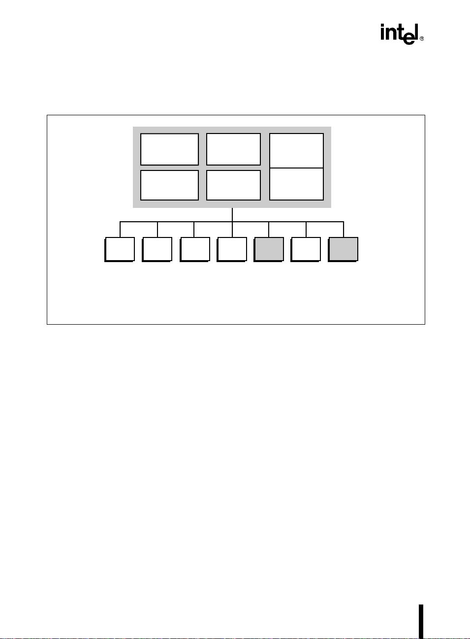
2.2 BLOCK DIAGRAM
Figure 2-1 is a simplified block diagram that shows the major blocks within the microcontroller.
Observe that the slave port peripheral does not exist on the 8XC196Lx.
Core
(CPU, Memory
Controller)
Clock and
Power Mgmt.
SIO
Note:
The J1850 peripheral is unique to the 87C196LB device.
The A/D peripheral is unique to the 87C196LA, LB devices.
Optional
ROM/
OTPROM
Optional
Code/Data
RAM
EPA
Controller
Peripheral
Transaction
A/DSSIOI/O
Interrupt
Server
WDT
J1850
A5253-01
Figure 2-1. 8XC196Lx Block Diagram
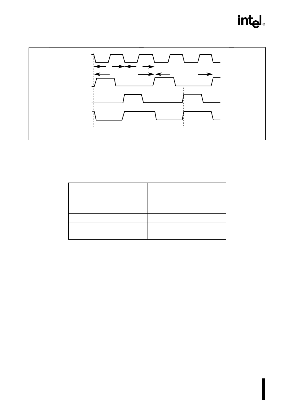
2.3 INTERNAL TIMING
The 87C196LA, LB clock circuitry (Figure 2-2) implements a phase-locked loo p and clock multiplier circuitry, which can substantially increase the CPU clock rate while using a lower-frequency input clock. The clock circuitry accepts an input clock signal on XTAL1 provided by an
external crystal or oscill ator. Depending on t he val u e of th e PLLEN pin, this frequency is routed
either through the phase-locked loop and m ultipl ier or directly to the divid e-by-two circuit. The
multiplier circuitry can double the input frequency (F
) before the frequency (f) reaches the
XTAL1
divide-by-two circuitry. The clock generators accept the divided input frequency (f/2) from the
divide-by-two circuit and produce two nonoverlapping internal timing signals, PH1 and PH2.
These signals are active when high.
2-2
NOTE
This manual uses lowercase “f” to represent the internal clock frequency. For
the 87C196LA and LB, f is equal to either F
XTAL1
or 2F
, depending on the
XTAL1
clock multiplier mode, which is controlled by the PLLEN input pin.
Page 17
ARCHITECTURAL OVERVIEW
XTAL1
XTAL2
F
XTAL1
Disable Oscillator
(Powerdown)
XTAL1
F
Disable
PLL
(Powerdown)
PLLEN
XTAL1
1
2F
0
Divide by two
Circuit
Clock
Generators
Programmable
Divider
(CLK1:0)
Phase
Comparator
Phase-locked
Oscillator
Phase-locked Loop
Clock Multiplier
f
Disable Clock Input (Powerdown)
f/2
Clock
Failure
Detection
f/2
Filter
To reset logic
Disable Clocks (Idle, Powerdown)
CPU Clocks (PH1, PH2)
Peripheral Clocks (PH1, PH2)
OSC
0
CLKOUT
1
Disable Clocks (Powerdown)
A5290-01
Figure 2-2. Clock Circuitry (87C196LA, LB Only)
The rising edges of PH1 and PH2 generate the internal CLKOUT signal (Figure 2-3). The clock
circuitry routes separat e internal cl ock sign als to the CPU an d the peri pherals to provi de flexi bility in power management. It also outputs the CLKOUT signal on the CLKOUT pin. Because of
the complex logic in the clock circuitry, the signal on the CLKOUT pin is a delayed version of
the internal CLKOUT signal. This delay varies with temperature and voltage.
2-3
Page 18
8XC196LX SUPPLEMENT
P H1 (in MHz)
f
2
-- - PH2==
XTAL1
PH1
PH2
CLKOUT
tt
1 State Time
1 State Time
Phase 1 Phase 2
Phase 1 Phase 2
A0805-01
Figure 2-3. Internal Clock Phases (Assumes PLL is Bypassed)
The combined period of phase 1 and phase 2 of the internal CLKOUT signal defines the basic
time unit known as a state time or state. T able 2 -2 lists state time durations at various frequencies.
Table 2-2. State Times at Various Frequencies
(Frequency Input to the
Divide-by-two Circuit)
f
State Time
8 MHz 250 ns
12 MHz 167 ns
16 MHz 125 ns
20 MHz 100 ns
The following formulas calculate the frequency of PH1 and PH2, the d uration of a state time, and
the duration of a clock period (t).
State Time (in µs)
2
-- -= t
f
1
-- -=
f
Because the device can operate at many frequencies, this manual defines time requirements (such
as instruction execution times) in terms of state times rather than specific measurements.
Datasheets list AC characteristics in terms of clock periods (t; sometimes called T
osc
).
Figure 2-4 illustrates the timing relationships between the input frequency (F
), the operating
XTAL1
frequency (f), and the CLKOUT signal with each PLLEN pin configuration. Table 2-3 details the
relationships between the input frequency (F
), the PLLEN pin, the operating frequency (f),
XTAL1
the clock period (t), and state times.
2-4
Page 19
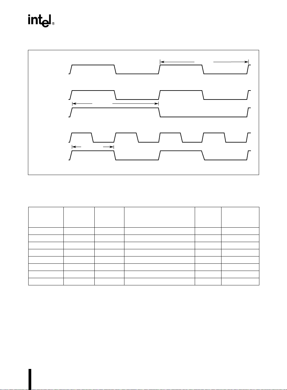
XTAL1
(16 MHz)
ARCHITECTURAL OVERVIEW
T
XHCH
PLLEN = 0
PLLEN = 1
f
t = 62.5ns
Internal
CLKOUT
f
t = 31.25ns
Internal
CLKOUT
A3376-01
Figure 2-4. Effect of Clock Mode on Internal CLKOUT Frequency
Table 2-3. Relationships Between Input Frequency, Clock Multiplier, and State Times
F
XTAL1
(Frequency
on XTAL1)
PLLEN Multiplier
(Input Frequency to
the Divide-by-two Circuit)
f
4 MHz 0 1 4 MHz 250 ns 500 ns
8 MHz 0 1 8 MHz 125 ns 250 ns
12 MHz 0 1 12 MHz 83.5 ns 167 ns
16 MHz 0 1 16 MHz 62.5 ns 125 ns
20 MHz 0 1 20 MHz 50 ns 100 ns
4 MHz 1 2 8 MHz 125 ns 250 ns
8 MHz 1 2 16 MHz 62.5 ns 125 ns
10 MHz 1 2 20 MHz 50 ns 100 ns
t
(Clock
Period)
State Time
2.4 EXTERNAL TIMING
You can control the output frequency on the CLKOUT pin by programming two uneraseable
PROM bits. Figure 2-5 illustrates the read-only USFR1, which reflects the state of the u nerasable
PROM bits. You can select one of three frequencies: f/2, f/4, or f/8. As Figure 2-2 on page 2-3
shows, the configurable divider accepts the output of the clock generators (f/2) and further divides that frequency to produce the desired output frequency. The CLK1:0 bits control the divisor
(divide f/2 by either 1, 2, or 4).
2-5
Page 20
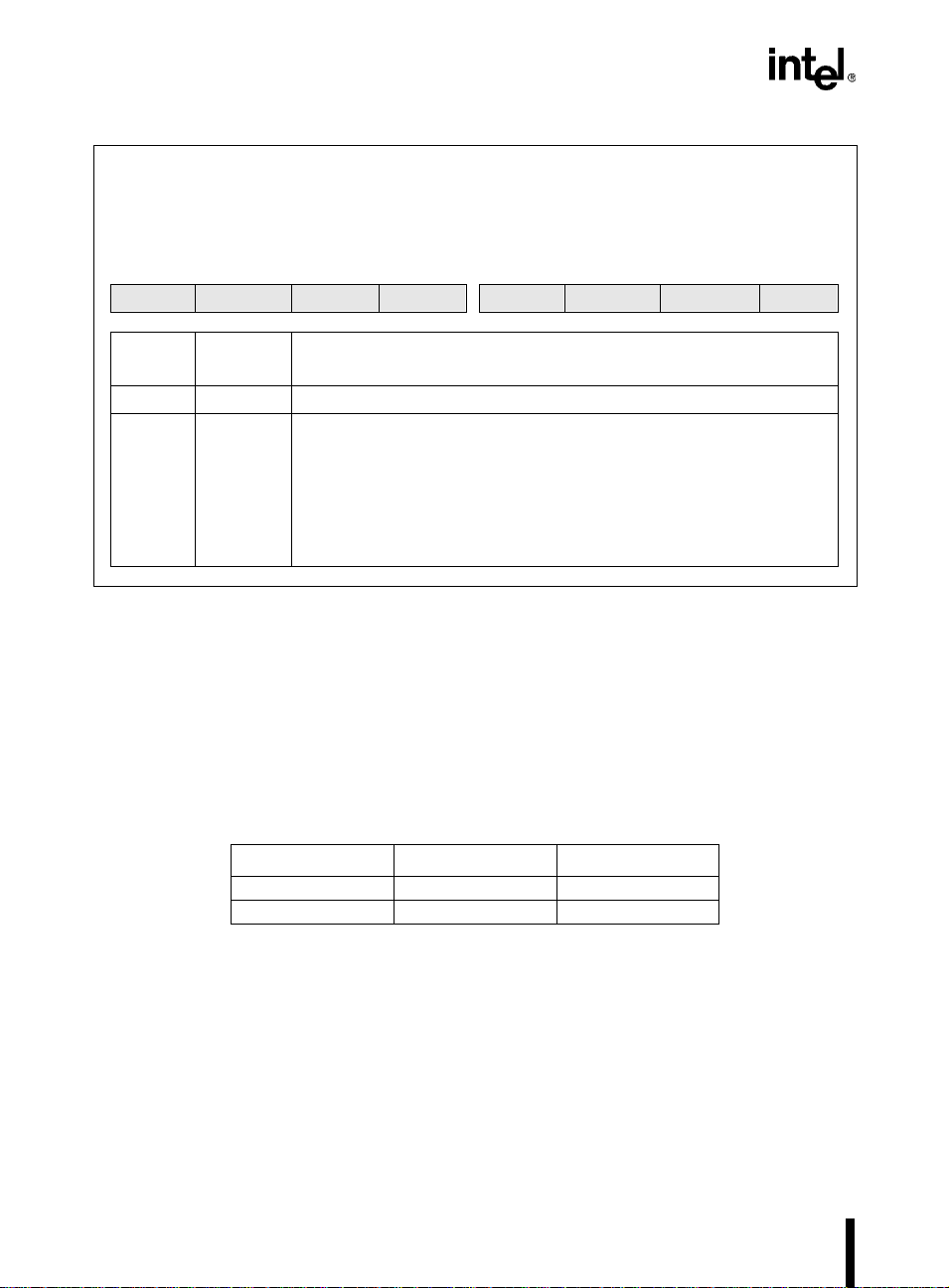
8XC196LX SUPPLEMENT
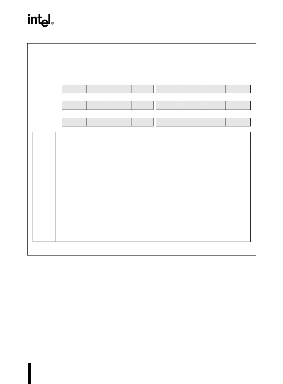
USFR1 (read only)
The UPROM special-function register 1 (USFR1) reflects the status of unerasable, programmable
read-only memory (UPROM) locations. This read-only register reflects the status of two bits that
control the output frequency on CLKOUT.
7 0
— — — — — — CLK1 CLK0
Bit
Number
7:2 — Reserved.
1:0 CLK1:0 CLKOUT Control
Bit
Mnemonic
Function
These bits reflect the programmed frequency of the CLKOUT signal:
CLK1 CLK0
0 0 divide by 1 (CLKOUT = f/2)
0 1 divide by 2 (CLKOUT = f/4)
1 0 divide by 4 (CLKOUT = f/8)
1 1 divide by 1 (CLKOUT = f/2)
Address:
Reset State:
1FF2H
XXH
Figure 2-5. Unerasable PROM 1 (USFR1) Register (LA, LB Only)
T o progr am these bits, write the co rrect value to the locations shown in Table 2-4 using slave programming mode. During normal operation , you can determine the values of these bits by reading
the UPROM SFR (Figure 2-5).
You can verify a UPROM bit to make sure it programmed, but you cannot erase it. For this reason, Intel cannot test the bits before shipment. However, Intel does test the features that t he UPROM bits enable, so the on ly undetectable defects ar e (unlikely) defects within the UPROM cells
themselves.
Table 2-4. UPROM Programming Values and Locations
To set this bit Write this value T o this location
CLK0 0001H 0768H
CLK1 0002H 0728H
2.5 INTERNAL PERIPHERALS
The internal peripheral modules provide special functions for a variety of applications. This section provides a brief description of the peripherals that differ between the 8XC196 Lx and the
8XC196Kx families.
2-6
Page 21

ARCHITECTURAL OVERVIEW
2.5.1 I/O Ports
The I/O ports of the 8XC196Lx are fu nctionally identical to those of th e 8XC196J x. However , on
the 87C196LA and LB the reset state level of all 41 general-purpose I/O pins has changed from
a weak logic “1” (wk1) to a weak logic “0” (wk0).
2.5.2 Synchronous Serial I/O Port
The synchronous serial I/O (SSIO) port on the 8XC196Lx has b een enhance d, implementing two
new special function registers (SSIO0_CLK and SSIO1_CLK) that allow you to select the operating mode and configure the phase and polarity of the serial clock signals.
2.5.3 Event Processor Array
The 8XC196L x’s event processor array (EPA) is functionally identical to that of the 8XC196Jx,
except that it has only two EPA capture/compare channels with out pins instead of four. In addition the LD has no compare-only channels.
2.5.4 J1850 Communications Controller
The 87C196LB microcon troller has a peri pheral no t found on the 8XC1 96Kx microcontrollers or
any other Lx microcontroller, the J1850 peripheral. The J1850 communications controller manages communications between multip le network nodes. This integrated peripheral s upports the
10.4 Kb/s VPW (variable pulse-width) medium-speed, class B, in-vehicle network protocol. It
also supports both the standard and in-frame response (IFR) message f raming as specified by the
Society of Automotive Engineering (SAE) J1850 (revised May 1994) technical standards.
2.6 DESIGN CONSIDERATIONS
With the exception of a few new multiplexed functions, the 8XC196Lx microcontrollers are pin
compatible with the 8XC1 96Jx microcontrollers . The 8XC196Jx microcontrollers are 52-lead
versions of 8XC196Kx microcontrollers. For registers that are implemented in both the
8XC196Lx and the 8XC196Jx, configure the 8XC196Lx register as y ou woul d fo r the 8XC 196Jx
unless differences are noted in this supplement.
2-7
Page 22

Page 23

Address Space
3
Page 24

Page 25

CHAPTER 3
ADDRESS SPACE
This chapter describes the differences in the address space of the 8XC196Lx from that of the
8XC196Kx.
3.1 ADDRESS PARTITIONS
Table 3-1 is an address map of the 8XC196Lx and 8XC196Kx microcontroller family members.
Table 3-1. Address Map
Device and Hex Address Range
JV
FFFF
E000
DFFF
2080
207F
2000
1FFF
1FE0
1FDF
1F00
1EFF
1E00
1DFF
1C00
FFFF
6000
5FFF
2080
207F
2000
1FFF
1FE0
1FDF
1F00
1EFF
1C00
LD
FFFF
8000
7FFF
2080
207F
2000
1FFF
1FE0
1FDF
1F00
1EFF
0300
LA, LB
JT, KT
FFFF
A000
9FFF
2080
207F
2000
1FFF
1FE0
1FDF
1F00
1EFF
1C00
CA
FFFF
A000
9FFF
2080
207F
2000
1FFF
1FE0
1FDF
1F00
1EFF
1E00
1DFF
1C00
—————
NOTES:
1. After a reset, the device fetches its first instruction from 2080H.
2. The content or function of these locations may change in future device revisions, in which case
a program that relies on a location in this range might not function properly.
JR, KR
FFFF
6000
5FFF
2080
207F
2000
1FFF
1FE0
1FDF
1F00
—————CAN SFRs
1EFF
1C00
Description
External device (memory
or I/O) connected to
address/data bus
Program memory
(internal nonvolatile or
external memory); see
Note 1
Special-purpose memory
(internal nonvolatile or
external memory)
Memory-mapped SFRs
Peripheral SFRs
(Includes J1850 SFRs on
87C196LB)
External device (memory
or I/O) connected to
address/data bus;
(future SFR expansion;
see Note 2)
Register RAM
Addressing
Modes
Indirect or
indexed
Indirect or
indexed
Indirect or
indexed
Indirect or
indexed
Indirect,
indexed, or
windowed
direct
Indirect,
indexed, or
windowed
direct
Indirect or
indexed
Indirect,
indexed, or
windowed
direct
3-1
Page 26

8XC196LX SUPPLEMENT
Table 3-1. Address Map (Continued)
Device and Hex Address Range
CA
1BFF
0500
04FF
0400
—
03FF
0100
00FF
0000
NOTES:
1. After a reset, the device fetches its first instruction from 2080H.
2. The content or function of these locations may change in future device revisions, in which case
a program that relies on a location in this range might not function properly.
JR, KR
1BFF
0500
04FF
0400
03FF
0200
01FF
0100
00FF
0000
LD
1BFF
0600
——
05FF
0180
017F
0100
00FF
0000
LA, LB
—
———
02FF
0100
00FF
0000
JT, KT
1BFF
0600
05FF
0400
03FF
0100
00FF
0000
JV
1BFF
0600
05FF
0400
03FF
0100
00FF
0000
Description
External device (memory
or I/O) connected to
address/data bus
Internal code or data RAM
External device (memory
or I/O) connected to
address/data bus
Upper register file
(general-purpose register
RAM)
Lower register file
(register RAM, stack
pointer, and CPU SFRs)
Addressing
Indirect or
indexed
Indirect or
indexed
Indirect or
indexed
Indirect,
indexed, or
windowed
direct
Direct,
indirect, or
indexed
Modes
3.2 REGISTER FILE
Figure 3-1 compares the register file addresses of the 8XC196Lx and 8XC196Kx. The register
file in Figure 3-1 is divi ded int o an upper register f ile and a lower regi ster fi le. The u pper register
file consists of general-purpose register RAM. The lower register file contains general-purpose
register RAM along with the stack pointer (SP) and the CPU special-function registers (SFRs).
T ab le 3-2 lists the register file memory addresses. The RALU accesses the lower register file directly, without the use of the memory controller. It also accesses a windowed location directly
(see “Windowing” on page 3-6). The upper register file and the peripheral SFRs can be win-
dowed. Registers in the lower register file and registers being windowed can be accessed with
register-direct addressing.
NOTE
The register file must not contain code. An attempt to execute an instruction
from a location in the register file causes the memory controller to fetch the
instruc tion from external memory.
3-2
Page 27
General-purpose
Register RAM
ADDRESS SPACE
Address
03FFH
(CA, JT, JV, KT)
02FFH (LA, LB)
01FFH (JR, KR)
017FH (LD)
Address
03FFH
0100H
00FFH
0000H
Upper
Register File
Lower
Register File
Figure 3-1. Register File Address Map
Table 3-2. Register File Memory Addresses
Device and Hex Address Range
JV CA,JT,KT LA, LB JR, KR LD
1DFF
1C00
03FF
0100
00FF
001A
0019
0018
0017
0000
— — — — Register RAM
03FF
0100
00FF
001A
0019
0018
0017
0000
02FF
0100
00FF
001A
0019
0018
0017
0000
01FF
0100
00FF
001A
0019
0018
0017
0000
017F
0100
00FF
001A
0019
0018
0017
0000
General-purpose
Register RAM
Stack Pointer
CPU SFRs
Description Addressing Modes
Upper register file (register RAM)
Lower register file (register RAM)
Lower register file (stack pointer)
Lower register file (CPU SFRs)
0100H
00FFH
001AH
0019H
0018H
0017H
0000H
A5260-01
Indirect, indexed, or
windowed direct
Indirect, indexed, or
windowed direct
Direct, indirect, or
indexed
Direct, indirect, or
indexed
Direct, indirect, or
indexed
3-3
Page 28
8XC196LX SUPPLEMENT
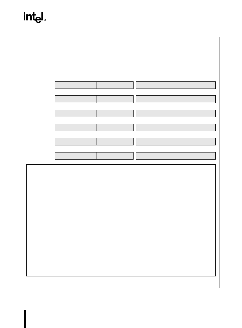
3.3 PERIPHERAL SPECIAL-FUNCTION REGISTERS
T ab le 3-3 l ist s the p eriph eral SF R addr esses . High light ed addr esses are un ique to t he 8 XC196L x.
T ab le 3- 3. 8XC19 6Lx Peripheral SFRs
Ports 3, 4, 5, and UPROM SFRs Ports 0, 1, 2, and 6 SFRs
Address High (Odd) Byte Low (Even) Byte Address High (Odd) Byte Low (Even) Byte
1FFEH P 4_PIN P3_PIN 1FDEH Reserved Reserved
1FFCH P4_REG P3_REG 1FDCH Reserved Reserved
1FFAH SLP_CON SLP_CMD 1FDAH Reserved P0_PIN
1FF8H Reserved SLP_STAT 1FD8H Reserved Reserved
1FF6H P5_PIN USFR 1FD6H P6_PIN P1_PIN
1FF4H P5_REG P34_DRV 1FD4H P6_REG P1_REG
1FF2H P5_DIR USFR1 (LA, LB) 1FD2H P6_DIR P1_DIR
1FF0H P5_MODE Reserved 1FD0H P6_MODE P1_MODE
1FEEH Reserved Reserved 1FCEH P2_PIN Reserved
1FECH Reserved Reserved 1FCCH P2_REG Reserved
1FEAH Reserved Reserved 1FCAH P2_DIR Reserved
1FE8H Reserved Reserved 1FC8H P2_MODE Reserved
1FE6H Reserved Reserved 1FC6H Reserved Reserved
1FE4H Reserved Reserved 1FC4H Reserved Reserved
1FE2H Reserved Reserved 1FC2H Reserved Reserved
1FE0H Reserved Reserved 1FC0H Reserved Reserved
†
Must be addressed as a word.
3-4
Page 29
ADDRESS SPACE
Table 3-3. 8XC196Lx Peripheral SFRs (Continued)
SIO and SSIO SFRs EPA SFRs (Continued)
Address High (Odd) Byte Low (Even) Byte Address High (Odd) Byte Low (Even) Byte
1FBEH Re served Reserved
1FBCH SP_BAUD (H) SP_BAUD (L) 1F7CH Reserved EPA7_CON
1FBAH SP_CON SBUF_TX
1FB8H SP_STATUS SBUF_RX 1F78H Reser ved EPA6_CON
1FB6H SSIO1_CLK Reserved
1FB4H SSIO0_CLK SSIO_BAUD 1F74H Reserved EPA5_CON
1FB2H SSIO1_CON SSIO1_BUF
1FB0H SSIO0_CON S SIO0_BUF 1F70H Reserved EPA4_CON
A/D SFRs (LA, LB Only)
Address High (Odd) Byte Low (Even) Byte
1FAEH AD_TIME AD_TEST
1FACH Reserved AD_COMMAND 1F68H Reserved EPA2_CON
1FAAH AD_RESULT (H) AD_RESULT (L)
EPA Interrupt SFRs
Address High (Odd) Byte Low (Even) Byte
1FA8H Reserved EPAIPV 1F60H Reserved EPA0_CON
1FA6H Reserved EPA_PEND1 J1850 SFRs (LB Only)
1FA4H Reserved EPA_MASK1 Address High (Odd) Byte Low (Even) Byte
†
1FA2H EP A_PEND (H) EPA_PEND (L) 1F5EH Reserved Reserved
†
1FA0H EPA_MASK (H) EPA_MASK (L) 1F5CH Reser ved Reserved
Timer 1, Timer 2, and EPA SFRs 1F5AH Reser ved Reserved
Address High (Odd) Byte Low (Even) Byte 1F58H Reserved J_DLY
†
1F9EH TIMER2 (H) TIMER2 (L) 1F56H Reserved Reserved
1F9CH Reserved T2CONTROL 1F54H Reserved J_CFG
†
1F9AH TIMER1 (H) TIMER1 (L) 1F52H J_STAT J_RX
1F98H Reserved T1CONTROL 1F50H J_CMD J_TX
1F96H Reserved Reserved
1F94H Reserved Reserved
1F92H Reserved RST_SRC
1F90H Reserved Reserved
EPA SFRs
Address High (Odd) Byte Low (Even) Byte
†
1F8EH COMP1_TIME (H) COMP1_TIME (L)
1F8CH Re served COMP1_CON
†
1F8AH COMP0_TIME (H) COMP0_TIME (L)
1F88H Reserved COMP0_CON
†
1F86H EPA9_TIME (H) E PA9_TIME (L)
1F84H Reserved EPA9_CON
†
1F82H EPA8_TIME (H) E PA8_TIME (L)
1F80H Reserved EPA8_CON
†
Must be addressed as a word.
†
1F7EH EPA7_TIME (H) EPA7_TIME (L)
†
1F7AH EPA6_TIME (H) EPA6_TIME (L)
†
1F76H EPA5_TIME (H) EPA5_TIME (L)
†
1F72H EPA4_TIME (H) EPA4_TIME (L)
†
1F6EH EPA3_TIME (H) EPA3_TIME (L)
†
1F6CH EPA3_CON (H) EPA3_CON (L)
†
1F6AH EPA2_TIME (H) EPA2_TIME (L)
†
1F66H EPA1_TIME (H) EPA1_TIME (L)
†
1F64H EPA1_CON (H) EPA1_CON (L)
†
1F62H EPA0_TIME (H) EPA0_TIME (L)
3-5
Page 30
8XC196LX SUPPLEMENT
3.4 WINDOWING
Windowing maps a segment of higher memory (the upper register file or peripheral SFRs) into
the lower register file. The window selection register (WSR) selects a 32-, 64- or 128-byte segment of higher memory to be windowed into the top of the lower register file space. Table 3-4
lists the WSR values for windowing the upper register file for both the 8XC196Lx and
8XC196Kx.
Table 3-4. Windows
Base
Address
Peripheral SFRs
1FE0H 7FH (Note)
1FC0H 7EH
1FA0H 7DH
1F60H 7BH
1F40H 7AH
1F20H 79H
CAN Peripheral SFRs (87C196CA Only)
1EE0H 77H
1EC0H 76H
1EA0H 75H
1E60H 73H
1E40H 72H
1E20H 71H
Register RAM (87C196JV Only)
1DE0H 6FH
1DC0H 6EH
1DA0H 6DH
1D60H 6BH
1D40H 6AH
1D20H 69H
NOTE: Locations 1FE0–1FFFH contain memory-mapped SFRs that cannot be accessed through a
window. Reading these locations through a window returns FFH; writing these locations
through a window has no effect.
WSR Value
for 32-byte Window
(00E0–00FFH)
WSR Value
for 64-byte Window
(00C0–00FFH)
3FH (Note)
3EH1F80H 7CH
3DH
3CH1F00H 78H
3BH
3AH1E80H 74H
39H
38H1E00H 70H
37H
36H1D80H 6CH
35H
34H1D00H 68H
WSR Value for
128-byte
Window
(0080–00FFH)
1FH (Note)
1EH
1DH
1CH
1BH
1AH
3-6
Page 31

ADDRESS SPACE
Table 3-4. Windows (Continued)
Base
Address
Register RAM (87C196JV Only; Continued)
1CE0H 67H
1CC0H 66H
1CA0H 65H
1C60H 63H
1C40H 62H
1C20H 61H
Upper Register File (CA, JT, JV, KT)
03E0H 5FH
03C0H 5EH
03A0H 5DH
0360H 5BH
0340H 5AH
0320H 59H
Upper Register File (CA, JT, JV, KT, LA, LB)
02E0H 57H
02C0H 56H
02A0H 55H
0260H 53H
0240H 52H
0220H 51H
Upper Register File (CA, JR, JT, JV, KR, KT, LA, LB)
01E0H 4FH
01C0H 4EH
01A0H 4DH
NOTE: Locations 1FE0–1FFFH contain memory-mapped SFRs that cannot be accessed through a
window. Reading these locations through a window returns FFH; writing these locations
through a window has no effect.
WSR Value
for 32-byte Window
(00E0–00FFH)
WSR Value
for 64-byte Window
(00C0–00FFH)
33H
32H1C80H 64H
31H
30H1C00H 60H
2FH
2EH0380H 5CH
2DH
2CH0300H 58H
2BH
2AH0280H 54H
29H
28H0200H 5 0H
27H
26H0180H 4CH
WSR Value for
128-byte
Window
(0080–00FFH)
19H
18H
17H
16H
15H
14H
13H
3-7
Page 32

8XC196LX SUPPLEMENT
Table 3-4. Windows (Continued)
Base
Address
Upper Register File (CA, JR, JT, JV, KR, KT, LA, LB, LD)
0160H 4BH
0140H 4AH
0120H 49H
NOTE: Locations 1FE0–1FFFH contain memory-mapped SFRs that cannot be accessed through a
window. Reading these locations through a window returns FFH; writing these locations
through a window has no effect.
WSR Value
for 32-byte Window
(00E0–00FFH)
WSR Value
for 64-byte Window
(00C0–00FFH)
25H
24H0100H 4 8H
WSR Value for
128-byte
Window
(0080–00FFH)
12H
3-8
Page 33

Standard and PTS
Interrupts
4
Page 34

Page 35

CHAPTER 4
STANDARD AND PTS INTERRUPTS
The interrupt structure of t he 8XC196Lx is the same as that of the 8XC196Jx. The o nly difference
is that the slave port interrupts (INT08:06) now support the J1850 controller peripheral.
4.1 INTERRUPT SOURCES, VECTORS, AND PRIORITIES
Ta ble 4-1 lists the 8XC196Lx’s interrupts sources, default priorities (30 is highest and 0 is lowest), and vector addresses.
4-1
Page 36

8XC196LX SUPPLEMENT
Table 4-1. Interrupt Sources, Vectors, and Priorities
Interrupt Source Mnemonic
Interrupt Controller
Service
PTS Service
†
Nonmaskable Interrupt NMI
Name
†
INT15 203EH 30 ———
Vector
Priority
Name
Vector
EXTINT Pin EXTINT INT14 203CH 14 PTS14 205CH 29
Reserved — INT13 203AH 13 PTS13 205AH 28
SIO Receive RI INT12 2038H 12 PTS12 2058H 27
SIO Transmit TI INT11 2036H 11 PTS11 2056H 26
SSIO Channel 1 Transfer SSIO1 INT10 2034H 10 PTS10 2054H 25
SSIO Channel 0 Transfer SSIO0 INT09 2032H 09 PTS09 2052H 24
J1850 Status (LB only) J1850ST INT08 2030H 08 PTS08 2050H 23
Reserved (LA, LD) — INT08 2030H 08 PTS08 2050H 23
Unimplemented Opcode — — 2012H — — — —
Software TRAP Instruction — — 2010H — — — —
J1850 Receive (LB only) J1850RX INT07 200EH 07 PTS07 204EH 22
Reserved (LA, LD) — INT07 200EH 07 PTS07 204EH 22
J1850 Transmit (LB only) J1850TX INT06 200CH 06 PTS06 204CH 21
Reserved (LA, LD) — INT06 200CH 06 PTS06 204CH 21
A/D Conv. Complete (LA, LB) AD_DONE INT05 200AH 05 PTS05 204AH 20
Reserved (LD) — INT05 200AH 05 PTS05 204AH 20
EPA Capture/Compare 0 EPA0 I NT04 2008H 04 PTS04 2048H 19
EPA Capture/Compare 1 EPA1 I NT03 2006H 03 PTS03 2046H 18
EPA Capture/Compare 2 EPA2 I NT02 2004H 02 PTS02 2044H 17
EPA Capture/Compare 3 EPA3 I NT01 2002H 01 PTS01 2042H 16
EPA Capture/Compare 6–9,
EPA 0–3, 8–9 Overrun,
EPA Compare 0–1
†††
,
x
INT00 2000H 00 PTS00 2040H 15
††
EPA
Timer 1 Overflow, &
Timer 2 Overflow
†
The NMI pin is not bonded out on the 8XC196Lx. To protect against glitches, create a dummy interrupt
service routine that contains a RET instruction.
††
These interrupts are individually prioritized in the EPAIPV register. Read the EPA pending registers
(EPA_PEND and EPA_PEND1) to determine which source caused the interrupt.
†††
87C196LA, LB only. The 83C196LD has no EPA compare-only channels.
Priority
4.2 INTERRUPT REGISTERS
This section describes the changes in the interrupt register bit definitions for the 8XC196Lx family.
4-2
Page 37

STANDARD AND PTS INTERRUPTS
4.2.1 Interrupt Mask Registers
Figures 4-1 and 4-2 illustrate the interrupt mask registers for the 8XC196Lx microcontrollers.
INT_MASK
Address:
Reset State:
0008H
00H
The interrupt mask (INT_MASK) register enables or disables (masks) individual interrupt requests.
(The EI and DI instructions enable and disable servicing of all maskable interrupts.) INT_MASK is the
low byte of the processor status word (PSW). PUSHF or PUSHA saves the contents of this register
onto the stack and then clears this register. Interrupt calls cannot occur immediately following a push
instruction. POPF or POPA restores it.
7 0
LA
— — AD EPA0 EPA1 EPA2 EPA3 EPA
x
7 0
LB
J1850RX J1850TX AD EPA0 EPA1 EPA2 EPA3 EPA
x
7 0
LD
Bit
Number
†
7:0
— — — EPA0 EPA1 EPA2 EPA3 EPA
Function
Setting a bit enables the corresponding interrupt.
x
Bit Mnemonic Interrupt Description
J1850RX J1850 Receive (LB only)
J1850TX J1850 Transmit (LB only)
AD A/D Conversion Complete (LA, LB)
EPA0 EPA Capture/Compare Channel 0
EPA1 EPA Capture/Compare Channel 1
EPA2 EPA Capture/Compare Channel 2
EPA3 EPA Capture/Compare Channel 3
††
x
EPA
††
EPA 6–9 capture/compare channel events, EPA 0–1 compare channel events
Shared EPA interrupt
†††
, EPA
0–3 and 8–9 capture/compare overruns, and timer overflows can generate this
x
multiplexed interrupt. The EPA mask and pending registers decode the EPA
interrupt.
Write the EPA mask registers to enable the interrupt sources; read the EPA pending
registers to determine which source caused the interrupt.
†††
87C196LA, LB only.
†
Bits 6–7 are reserved on the 87C196LA, and bits 5–7 are reserved on the 83C196LD. For
compatibility with future devices, write zeros to these bits.
Figure 4-1. Interrupt Mask (INT_MASK) Register
4-3
Page 38

8XC196LX SUPPLEMENT
INT_MASK1
Address:
Reset State:
0013H
00H
The interrupt mask 1 (INT_MASK1) register enables or disables (masks) individual interrupt requests.
(The EI and DI instructions enable and disable servicing of all maskable interrupts.) INT_MASK1 can
be read from or written to as a byte register. PUSHA saves this register on the stack and POPA
restores it.
7 0
LB
NMI EXTINT — RI TI SSIO1 SSIO0 J1850ST
7 0
LA, LD
Bit
Number
†
7:0
NMI EXTINT — RI TI SSIO1 SSIO0 —
Function
Setting a bit enables the corresponding interrupt.
Bit Mnemonic Interrupt Description
NMI
††
Nonmaskable Interrupt
EXTINT EXTINT Pin
Reserved —
RI SIO Receive
TI SIO Transmit
SSIO1 SSIO1 Tr ansfer
SSIO0 SSIO0 Tr ansfer
J1850ST J1850 Status (LB only)
††
NMI is always enabled. This nonfunctional mask bit exists for design symmetry with the
INT_PEND1 register. Always write zero to this bit.
†
Bit 5 is reserved on the 8XC196Lx devices, and bit 0 is reserved on the 87C196LA and 83C196LD.
For compatibility with future devices, always write zeros to these bits.
Figure 4-2. Interrupt Mask 1 (INT_MASK1) Register
4.2.2 Interrupt Pending Registers
Figures 4-3 and 4-4 illustrate the interrupt pending registers for the 8XC196Lx microcontrollers.
4-4
Page 39
STANDARD AND PTS INTERRUPTS
INT_PEND
Address:
Reset State:
0009H
00H
When hardware detects an interrupt request, it sets the corresponding bit in the interrupt pending
(INT_PEND or INT_PEND1) registers. When the vector is taken, the hardware clears the pending bit.
Software can generate an interrupt by setting the corresponding interrupt pending bit.
7 0
LA
— — AD EPA0 EPA1 EPA2 EPA3 EPA
x
7 0
LB
J1850RX J1850TX AD EPA0 EPA1 EPA2 EPA3 EPA
x
7 0
LD
Bit
Number
†
7:0
— — — EPA0 EPA1 EPA2 EPA3 EPA
Function
Any set bit indicates that the corresponding interrupt is pending. The interrupt bit is cleared
x
when processing transfers to the corresponding interrupt vector.
Bit Mnemonic Interrupt Description
J1850RX J1850 Receive (LB only)
J1850TX J1850 Transmit (LB only)
AD A/D Conversion Complete (LA, LB)
EPA0 EPA Capture/Compare Channel 0
EPA1 EPA Capture/Compare Channel 1
EPA2 EPA Capture/Compare Channel 2
EPA3 EPA Capture/Compare Channel 3
††
x
EPA
††
EPA 6–9 capture/compare channel events, EPA 0–1 compare channel events
Shared EPA Interrupt
†††
, EP A
0–3 and 8–9 capture/compare overruns, and timer overflows can generate this shared
interrupt. Write the EPA mask registersto enable the interrupt sources; read the EPA
pending registers to determine which source caused the interrupt.
†††
87C196LA, LB only.
†
Bits 6–7 are reserved on the 87C196LA, and bits 5–7 are reserved on the 83C196LD. For
compatibility with future devices, write zeros to these bits.
Figure 4-3. Interrupt Pending (INT_PEND) Register
4-5
Page 40
8XC196LX SUPPLEMENT
INT_PEND1
When hardware detects an interrupt request, it sets the corresponding bit in the interrupt pending
(INT_PEND or INT_PEND1) registers. When the vector is taken, the hardware clears the pending bit.
Software can generate an interrupt by setting the corresponding interrupt pending bit.
7 0
LB
LA, LD
Bit
Number
†
7:0
†
Bit 5 is reserved on the 8XC196Lx devices and bit 0 is reserved on the 87C196LA and 83C196LD.
For compatibility with future devices, always write zeros to these bits.
NMI EXTINT — RI TI SSIO1 SSIO0 J1850ST
7 0
NMI EXTINT — RI TI SSIO1 SSIO0 —
Function
Any set bit indicates that the corresponding interrupt is pending. The interrupt bit is cleared
when processing transfers to the corresponding interrupt vector.
Bit Mnemonic Interrupt Description
NMI Nonmaskable Interrupt
EXTINT EXTINT Pin
Reserved —
RI SIO Receive
TI SIO Transmit
SSIO1 SSIO 1 Transfer
SSIO0 SSIO 0 Transfer
J1850ST J1850 Status (LB only)
Address:
Reset State:
0012H
00H
Figure 4-4. Interrupt Pending 1 (INT_PEND1) Register
4.2.3 Peripheral Transaction Server Registers
Figures 4-5 and 4-6 illustrate the PTS interrupt select and service registers for the 8XC196Lx microcontrollers.
4-6
Page 41
STANDARD AND PTS INTERRUPTS
PTSSEL
Address:
Reset State:
0004H
0000H
The PTS select (PTSSEL) register selects either a PTS microcode routine or a standard interrupt
service routine for each interrupt request. Setting a bit selects a PTS microcode routine; clearing a bit
selects a standard interrupt service routine. In PTS modes that use the PTSCOUNT register, hardware
clears the corresponding PTSSEL bit when PTSCOUNT reaches zero. The end-of-PTS interrupt service
routine must reset the PTSSEL bit to re-enable the PTS channel.
15 8
LA
— EXTINT — RI TI SSIO1 SSIO0
—
7 0
— — AD EPA0 EPA1 EPA2 EPA3 EPA
x
15 8
LB
— EXTINT — RI TI SSIO1 SSIO0
J1850ST
7 0
J1850RX J1850TX AD EPA0 EPA1 EPA2 EPA3 EPA
x
15 8
LD
— EXTINT — RI TI SSIO1 SSIO0 —
7 0
Bit
Number
†
14:0
— — — EPA0 EPA1 EPA2 EPA3 EPA
Function
Setting a bit causes the corresponding interrupt to be handled by a PTS microcode routine.
x
The PTS interrupt vector locations are as follows:
Bit Mnemonic Interrupt PTS Vector
EXTINT EXTINT pin 205CH
Reserved
†
— 205AH
RI SIO Receive 2058H
TI S IO Transmit 2056H
SSIO1 SSIO 1 Transfer 2054H
SSIO0 SSIO 0 Transfer 2052H
J1850ST (LB) J1850 Status 2050H
J1850RX(LB) J1850 Receive 204EH
J1850TX(LB) J1850 Transmit 204CH
AD(LA, LB) A/D Conversion Complete 204AH
EPA0 EPA Capture/Compare Channel 0 2048H
EPA1 EPA Capture/Compare Channel 1 2046H
EPA2 EPA Capture/Compare Channel 2 2044H
EPA3 EPA Capture/Compare Channel 3 2042H
††
x
EPA
††
PTS service is not useful for shared interrupts because the PTS cannot readily
Multiplexed EPA 2040H
determine the source of these interrupts.
†
Bit 13 is reserved on the 8XC196Lx devices and bits 6–8 are reserved on the 87C196LA and
83C196LD. For compatibility with future devices, write zeros to these bits.
Figure 4-5. PTS Select (PTSSEL) Register
4-7
Page 42

8XC196LX SUPPLEMENT
PTSSRV
Address:
Reset State:
0006H
0000H
The PTS service (PTSSRV) register is used by the hardware to indicate that the final P TS interrupt has
been serviced by the PTS routine. When PTSCOUNT reaches zero, hardware clears the corresponding
PTSSEL bit and sets the PTSSRV bit, which requests the end-of-PTS interrupt. When the end-of-PTS
interrupt is called, hardware clears the PTSSRV bit. The end-of-PTS interrupt service routine must set
the PTSSEL bit to re-enable the PTS channel.
15 8
LA
— EXTINT — RI TI SSIO1 SSIO0
—
7 0
— — AD EPA0 EPA1 EPA2 EPA3 EPA
x
15 8
LB
— EXTINT — RI TI SSIO1 SSIO0
J1850ST
7 0
J1850RX J1850TX AD EPA0 EPA1 EPA2 EPA3 EPA
x
15 8
LD
— EXTINT — RI TI SSIO1 SSIO0 —
7 0
— — — EPA0 EPA1 EPA2 EPA3 EPA
x
Bits Function
†
14:0
A bit is set by hardware to request an end-of-PTS interrupt for the corresponding interrupt
through its standard interrupt vector.
The standard interrupt vector locations are as follows:
Bit Mnemonic Interrupt Standard Vector
EXTINT EXTINT pin 203CH
Reserved
†
— 203AH
RI SIO Receive 2038H
TI S IO Transmit 2036H
SSIO1 SSIO 1 Transfer 2034H
SSIO0 SSIO 0 Transfer 2032H
J1850ST (LB) J1850 Status 2030H
J1850RX (LB) J1850 Receive 202EH
J1850TX (LB) J1850 Transmit 202CH
AD (LA, LB) A/D Conversion Complete 202AH
EPA0 EPA Capture/Compare Channel 0 2028H
EPA1 EPA Capture/Compare Channel 1 2026H
EPA2 EPA Capture/Compare Channel 2 2024H
EPA3 EPA Capture/Compare Channel 3 2022H
††
x
EPA
††
PTS service is not useful for shared interrupts because the PTS cannot readily
Multiplexed EPA 2020H
determine the source of these interrupts.
†
Bit 13 is reserved on the 8XC196Lx devices and bits 6–8 are reserved on the 87C196LA and
83C196LD. For compatibility with future devices, write zeros to these bits.
Figure 4-6. PTS Service (PTSSRV) Register
4-8
Page 43

I/O Ports
5
Page 44

Page 45

CHAPTER 5
I/O PORTS
The I/O ports of the 8XC196Lx are fu nctionally identical to those of th e 8XC196J x. However , on
the 87C196LA and LB, the reset state level of all 41 general-purpose I/O pins has changed from
a weak logic “1” (wk1) to a weak logic “0” (wk0). This chapter outlines the differences between
the 87C196LA, LB and the 8XC196Kx controllers.
5.1 I/O PORTS OVERVIEW
Table 5-1 provides an overview of the 8XC196Lx and 8XC196Kx I/O ports.
T a ble 5-1. Mic rocontroller Ports
Port Pins Type
x
)
Port 0
Port 1
Port 2
Port 3 8 Memory mapped
Port 4 8 Memory mapped
Port 5
Port 6
8 (K
6 (CA, J
x
)
8 (K
4 (CA, J
x
)
8 (K
6 (CA, J
x
)
8 (K
3 (CA, J
x
)
8 (K
6 (CA, J
Standard Input-only
x, Lx
)
Standard
x, Lx
)
Standard
x, Lx
)
Memory mapped
x, Lx
)
Standard
x, Lx
)
Configuration
Options
Complementary
Open-drain
Complementary
Open-drain
Complementary
Open-drain
Complementary
Open-drain
Complementary
Open-drain
Complementary
Open-drain
Associated Peripheral or
System Function
A/D converter
(not supported on LD)
EPA and timers
J1850 (LB only), SIO,
interrupts, bus control, clock
gen.
Address/data bus
Address/data bus
Bus control, slave port
EPA, SSIO
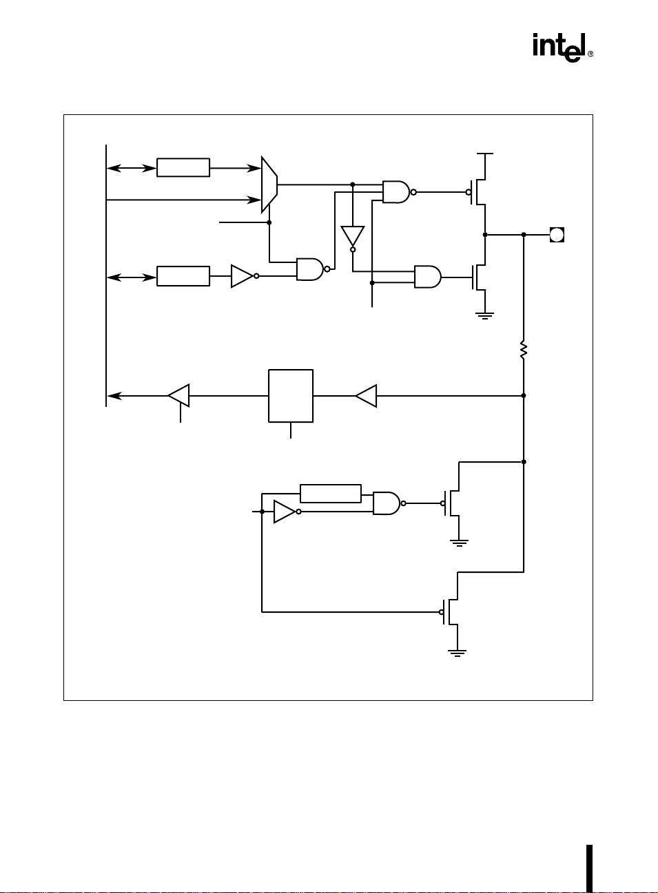
5.2 INTERNAL STRUCTURE FOR PORTS 1, 2, 5, AND 6 (BIDIRECTIONAL
PORTS)
Figure 5-1 shows the logic for driving the output transistors, Q1 and Q2. Consult the datasheet
for specifications on the amount of current that each port can source or sink.
In I/O mode (selected by clearing a port mode register bit), the port data output and the port direction registers are input to the multiplexers. These signals combine to drive the gates of Q1 and
Q2 so that the outp ut is high, low, or high impedance.
In special-function mode (selected by setting a port mode register bit), SFDIR and SFDATA are
input to the multiplexers. These signals combine to drive the gates of Q1 and Q2 so that the output
is high, low, or high impedance. Special-function output signals clear SFDIR; special-function
5-1
Page 46

8XC196LX SUPPLEMENT
input signals set SFDIR. Even if a pin is to be u sed in special-fun ction m ode, y ou mu st still in itialize the pin as an input or output by writing to the port direction reg ister.
Resistor R1 provides ESD protection for the pin. Input signals are buffered. The standard ports
use Schmitt-triggered buffers for improved noise immunit y. Port 5 uses a standard input buffer
because of the high speeds required for bus contro l functions. The signals ar e latched into the port
pin register sample latch and output onto the internal bus when the port pin register is read.
The falling edge of RESET# turns on transistor Q3, which remains on for about 300 ns, causing
the pin to change rapidly to its reset state. The active-low level of RESET# turns on transistor Q4,
which weakly holds the pin low. Q4 remains on, weakly holding the pin low, until your software
writes to the port mode register.
NOTE
P2.7 is an exception. After reset, P2.7 carries the CLKOUT signal (half the
crystal input frequency) rather than being held low. When CLKOUT is
selected, it is always a complementary output.
5-2
Page 47

I/O PORTS
Internal Bus
Px_REG
SFDATA
Px_DRV
SFDIR
Px_MODE
Read Port
RESET#
0
1
0
1
Sample
Latch
Px_PIN
LE
PH1 Clock
300ns Delay
V
CC
Q1
I/O Pin
Q2
RESET#
Buffer
DQ
V
SS
150Ω to 200Ω
Medium
Pullup
Q3
R1
V
SS
Weak
RESET#
Any Write to Px_MODE
R
Q
S
Pullup
Q4
V
SS
A5265-01
Figure 5-1. Ports 1, 2, 5, and 6 Internal Structure (87C196LA, LB Only)
5.2.1 Configuring Ports 1, 2, 5, and 6 (Bidirectional Ports)
Using the port mode register, you can individually configure each pin for port 1, 2, 5, and 6 to
operate either as a general-purpose I/O signal (I/O mode) or as a special-function signal (specialfunction mode). In either mode, three configurations are possible: complementary output, high-
5-3
Page 48

8XC196LX SUPPLEMENT
impedance input, or open-drain out put. The port direction and data output reg isters select t he configuration for each pin. Complementary output means that the microcontroller drives the signal
high or low. High-impedance input means that the microcontroller floats the signal. Open-drain
output means that the microcontroller drives the si gnal low or floats it. For I/O mode, the port
data output register determines whether the microcontroller drives the signal high , drives it low,
or floats it. For special-function mode, the on-chip peripheral or system function determines
whether the microcontroller drives the signal high or low for complementary outputs.
The pins for por ts 1, 2, 5, and 6 are weakly p ul le d lo w d uri ng an d after reset. Initializi ng the pins
by writing to the port mode register turns off the weak pull-downs. To ensure that the ports are
initialized correctly, follow this suggested initialization sequence:
1. Write to Px_DIR to configure the individual pins. Clearing a bit configures a pin as a
complementary output. Setting a bit configures a pin as a high-impedance input or opendrain output.
2. Write to Px_MODE to select either I/O or special-function mode. Writing to Px_MODE
(regardless of the value written) turns off the weak pull-downs. Even if the entire port is to
be used as I/O (its default configuration after reset), you must write to Px_MODE to
ensure that the weak pull-downs are turned off.
3. Write to Px_REG.
For complementary output configurations:
In I/O mode, write the data that is to be driven by the pins to the corresponding Px_REG
bits. In special-function mode, the value is immaterial because the on-chip peripheral or
system function controls the pin. However, you must still write to Px_REG to initialize the
pin.
For high-impedance input or open-drain output configurations:
In I/O mode, write to Px_REG to either float the pin, making it available as a high
impedance input, or pull it low. Setting the corresponding Px_REG bit floats the pin;
clearing the corresponding Px_REG bit pulls the pin low. In special-function mode, if the
on-chip peripheral uses the pin as an input signal, you must set the corresponding Px_REG
bit so that the pin can be driven externally. If the on-chip peripheral uses the pin as an
output signal, the value of the corresponding Px_REG bit is immaterial because the onchip peripheral or system function controls the pin . Howev e r, you must still write to
Px_REG to initialize the pin.
5.2.2 Special Bidirectional Port Considerations
This section outlines special considerati on for using the pins of ports 1, 2, 5, and 6.
1. After reset, your software must configure the device to match the external system. This
accomplished by writing appropriate configuration data into Px_MODE. Writing to
Px_MODE not only configures the pins but also turns off the transistor that weakly holds
the pins low. For this reason, even if your port is to be used as it is configured at reset, you
should still write data into Px_MODE.
2. P2.6/TXJ1850 is the enable pin for ONCE mode. Because a high input during reset can
cause the device to enter ONCE mode or a reserved test mode, caution must be exercised
5-4
Page 49

I/O PORTS
in using this pin. Be certain that your system meets the VIH specifications during reset to
prevent inadvertent entry into ONCE mode or a test mode.
3. Following reset, P2.7/CLKOUT carries the strongly driven CLKOUT signal. It is not held
low. When P2.7/CLKOUT is configured as CLKOUT, it is always a complementary
output.
5.3 INTERNAL STRUCTURE FOR PORTS 3 AND 4 (ADDRESS/DATA BUS)
Figure 5-2 shows the lo gic of ports 3 and 4. Co nsult the datasheet for specifications on the amo unt
of current ports 3 and 4 can source and sink.
During reset, the active-low level of RESET# turns off Q1 and Q2 an d turns on transistor Q4,
which weakly holds the pin low. Resistor R1 provides ESD protection for the pin. During normal
operation, the device controls the port through BUS CONTROL SELECT , an internal control signal.
When the device needs to access external memory, it clears BUS CONTROL SELECT, selecting
ADDRESS/DATA as the input to the multiplexer. ADDRESS/DATA then drives Q1 and Q2 as
complementary ou tputs.
When external memory access is not required, the device sets BUS CONTROL SELECT, selecting Px_REG as the input to the multiplexer. Px_REG then drives Q1 and Q2. If P34_DRV is set,
Q1 and Q2 are driven as complementary outputs. If P34_DRV is cleared, Q1 is disabled and Q2
is driven as an open-drain output requiring an external pull-up resistor. With the open-drain configuration (BUS CONTROL SELECT set and P34_DRV cleared) and Px_REG set, the pin can
be used as an input. The signal on the pin is latched in the Px_PIN register . The pins can be read,
making it easy to see which pins are driven low by the device and which are driven high by external drivers while in open-drain mode.
5-5
Page 50
8XC196LX SUPPLEMENT
Internal Bus
Px_REG
Address/Data
Bus Control Select
0 = Address/Data
1 = I/O
P34_DRV
Read Port
RESET#
1
0
Sample
Latch
Px_PIN
LE
PH1 Clock
DQ
300ns Delay
RESET#
Buffer
V
CC
Q1
Q2
V
SS
150Ω to 200Ω
Medium
Pullup
Q3
I/O Pin
R1
5-6
V
SS
Weak
Pullup
Q4
V
SS
Figure 5-2. Ports 3 and 4 Internal Structure (87C196LA, LB Only)
A5264-01
Page 51

Synchronous Serial
I/O Port
6
Page 52

Page 53

CHAPTER 6
SYNCHRONOUS SERIAL I/O PORT
The synchronous serial I/O (SSIO) port on the 8XC196Lx has b een enhance d, implementing two
new special function registers (SSIO0_CLK and SSIO1_CLK) that allow you to select the operating mode and configure the phase and polarity of the serial clock signals.
6.1 SSIO 0 CLOCK REGISTER
The SSIO 0 clock (SSIO_CLK) register selects the phase and polarity for the SC0 clock signal.
In standard mode, SC0 is channel 0’s clock signal. In duplex and channel-select modes, SC0 is
the common clock signal for both SSIO channels.
SSIO0_CLK
The SSIO 0 clock (SSIO0_CLK) register configures the serial clock for channel 0. In standard mode,
the SC0 is channel 0’s clock signal. In duplex and channel-select modes, SC0 is the common clock
signal for both SSIO channels.
7 0
— — — — — — PHAS POLS
Bit
Number
7:2 — Reserved; for compatibility with future devices, write zeros to these bits.
1 PH AS Phase and Polarity Select
0POLS
Bit
Mnemonic
Function
For normal transfers, these bits determine the idle state of the serial
clock and select the serial clock signal edge on which the SSIO samples
incoming data bits or shifts out outgoing data bits. These bits are ignored
for handshaking transfers. Use SSIO0_ CON to select the type of data
transfer (normal or handshaking) for channel 0.
For transmissions
PHAS POLS
0 0 low idle state; shift on falling edges
0 1 high idle state; shift on rising edges
1 0 low idle state; shift on rising edges
1 1 high idle state; shift on falling edges
For receptions
PHAS POLS
0 0 low idle state; sample on rising edges
0 1 high idle state; sample on falling edges
1 0 low idle state; sample on falling edges
1 1 high idle state; sample on rising edges
Address:
Reset State:
1FB5H
00H
Figure 6-1. SSIO 0 Clock (SSIO0_CLK) Register
6-1
Page 54

8XC196LX SUPPLEMENT
For transmissions, SSIO0_CLK determines whether the SSIO shifts out data bits on rising or falling clock edges. For receptions, SSIO0_CLK determines whether the SSIO samples data bits on
rising or falling clock edges.
6.2 SSIO 1 CLOCK REGISTER
SSIO1_CLK selects the SSIO mode of operation (standard, duplex, or channel-select), enables
the channel-select master contention interrupt request, and selects the phase and polarity for the
serial clock (SC1) for channels. In standard mode, use this register to configure the serial clock
for channel 1.
SSIO1_CLK
The SSIO 1 clock (SSIO1_CLK) register selects the SSIO mode of operation (standard, duplex, or
channel-select), enables the channel-select master contention interrupt request, and selects the
phase and polarity for the serial clock (SC1) for channel 1.
7 0
— — CHS DUP CONINT CONPND PHAS POLS
Address:
Reset State:
1FB7H
00H
Bit
Number
7:6 — Reserved; for compatibility with future devices, write zeros to these bits.
5 CHS These bits determine the SSIO operating mode.
4 DUP
3 CONINT Master Contention Interrupt
Bit
Mnemonic
Function
CHS DUP
0 0 standard mode
0 1 duplex mode
1 0 channel-select half-duplex mode (uses SD1 only)
1 1 channel-select full-duplex mode (uses both SD0 and SD1)
For channel-select master operations, the SSIO sets the master
contention interrupt pending bit (CONPND) when the CHS# pin is
externally activated. In a system with multiple masters, an external
master activates the CHS# signal to request control of the serial clock.
CONINT determines whether the SSIO sets both CONPND and the
SSIO0 interrupt pending bit or only CONPND when the CHS# pin is
externally activated.
0 = SSIO sets only CONPND
1 = SSIO sets both CONPND and the SSIO0 interrupt pending bit
This bit is valid for channel-select master operations and ignored for all
other operations.
Figure 6-2. SSIO 1 Clock (SSIO1_CLK) Register
6-2
Page 55

SYNCHRONOUS SERIAL I/O PORT
SSIO1_CLK (Continued)
The SSIO 1 clock (SSIO1_CLK) register selects the SSIO mode of operation (standard, duplex, or
channel-select), enables the channel-select master contention interrupt request, and selects the
phase and polarity for the serial clock (SC1) for channel 1.
7 0
— — CHS DUP CONINT CONPND PHAS POLS
Bit
Number
2 CONPN D Master Contention Interrupt Pending
1 PH AS Phase and Polarity Select
0POLS
Bit
Mnemonic
Function
For channel-select master operations, the SSIO sets this bit when the
CHS# pin is externally activated. In a system with multiple masters, an
external master activates the CHS# signal to request control of the serial
clock.
This bit is valid for channel-select master operations and ignored for all
other operations.
For normal transfers, these bits determine the idle state of the serial
clock and select the serial clock signal edge that the SSIO samples
incoming data bits or shifts out outgoing data bits.
For transmissions
PHAS POLS
0 0 low idle state; shift on falling edges
0 1 high idle state; shift on rising edges
1 0 low idle state; shift on rising edges
1 1 high idle state; shift on falling edges
For receptions
PHAS POLS
0 0 low idle state; sample on rising edges
0 1 high idle state; sample on falling edges
1 0 low idle state; sample on falling edges
1 1 high idle state; sample on rising edges
These bits are ignored for duplex and channel-select modes; these
modes use SC0 as the common clock signal. The SSIO0_CLK register
contains the phase and polarity select bits for the SC0 clock signal.
These bits are also ignored for handshaking transfers. Use SSIO1_ CON
to select the type of data transfer (normal or handshaking) for channel 1.
Address:
Reset State:
1FB7H
00H
Figure 6-2. SSIO 1 Clock (SSIO1_CLK) Register (Continued)
For transmissions, SSIO1_CLK determines whether the SSIO shifts out data bits on rising or falling clock edges. For receptions, SSIO1_CLK determines whether the SSIO samples data bits on
the rising or falling clock edges.
6-3
Page 56

Page 57

Event Processor
Array
7
Page 58

Page 59
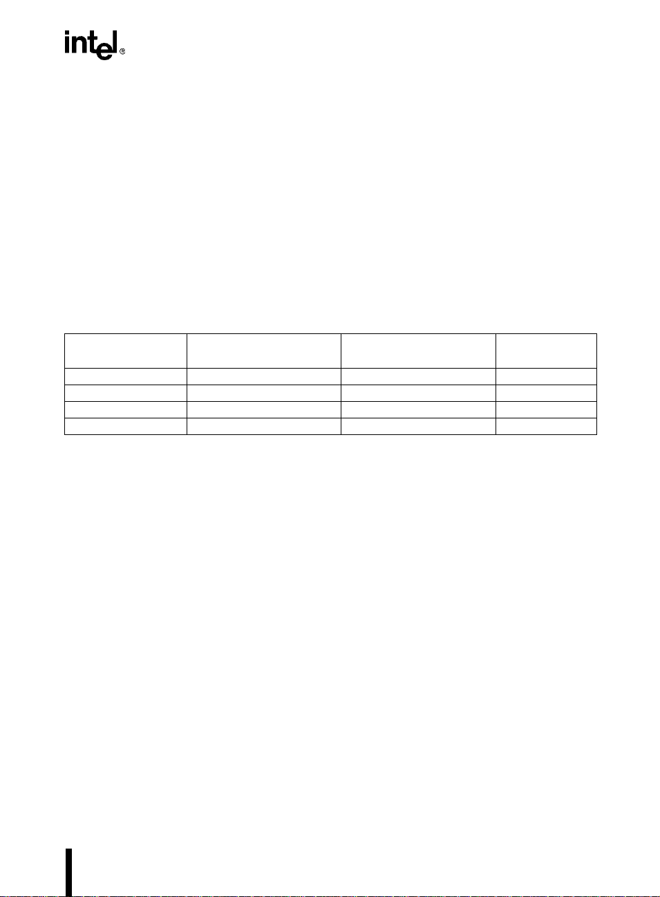
CHAPTER 7
EVENT PROCESSOR ARRAY
The EPA on the 8XC196Lx is functionally identical to that of the 8XC196Jx; however, the
8XC196Lx has only two capture/compare channels without pins instead of four. In addition, the
83C196LD has no compare-only channels.
7.1 EPA FUNCTIONAL OVERVIEW
Table 7-1 lists the capture/compare (with and without pins) and compare-only channels for each
device in the 8XC196Lx and 8XC196Kx families.
Table 7-1. EPA Channels
Device
8XC196LA, LB EPA3:0 and EPA9:8 EPA7:6 COMP1:0
8XC196LD EPA3:0 and EPA9:8 EPA7:6 —
87C196CA, 8XC196J
8XC196K
x
x
Capture/Compare
Channels With Pins
EPA3:0 and EPA9:8 EPA7:4 COMP1:0
EPA9:0 — COMP1:0
The 8XC196Lx’s EPA performs input and output functions associated with two timer/counters,
timer 1 and timer 2, as depicted in Figures 7-1 and 7-2.
Capture/Compare
Channels Without Pins
Compare-only
Channels
7-1
Page 60

8XC196LX SUPPLEMENT
Timer-Counter Unit
TIMER1
TIMER2
EPA 3:0
EPA8 / COMP0
EPA9 / COMP1
Capture/Compare
Channel 0–3
Capture/Compare
Channel 6–7
Capture/Compare
Channel 8
Compare-only
Channel 0
Capture/Compare
Channel 9
Compare-only
Channel 1
EPA 3:0 Interrupts
Indirect
Interrupt
Processor
Logic
Figure 7-1. EPA Block Diagram (87C196LA, LB Only)
EPA
x
Interrupt
A5269-01
7-2
Page 61

Timer-Counter Unit
TIMER1
TIMER2
EVENT PROCESSOR ARRAY
EPA 3:0
EPA8
EPA9
Capture/Compare
Channel 0–3
Capture/Compare
Channel 6–7
Capture/Compare
Channel 8
Capture/Compare
Channel 9
EPA 3:0 Interrupts
Indirect
Interrupt
Processor
Logic
Figure 7-2. EPA Block Diagram (83C196LD Only)
EPA
x
Interrupt
A5281-01
7-3
Page 62

8XC196LX SUPPLEMENT
7.1.1 EPA Mask Registers
Figures 7-3 and 7-4 illustrate the EPA mask registers, EPA_MASK and EPA_MASK1, for the
8XC196Lx microcontroller family.
EPA_MASK
The EPA interrupt mask (EPA_MASK) register enables or disables (masks) interrupts associated with
the shared EPA
Lx
Bit
Number
†
15:0
†
Bits 2–5 and 14–15 are reserved on the 8XC196Lx device family. For compatibility with future
devices, write zeros to these bits.
x
interrupt.
15 8
— — EPA6 EPA7 EPA8 EPA9 OVR0 OVR1
7 0
0VR2 OVR3 — — — — OVR8 OVR9
Function
Setting a bit enables the corresponding interrupt as a EPAx interrupt source. The shared
x
interrupt is enabled by setting its interrupt enable bit in the interrupt mask register
EPA
(INT_MASK.0 = 1).
Address:
Reset State:
1FA0H
0000H
Figure 7-3. EPA Interrupt Mask (EPA_MASK) Register
EPA_MASK1
The EPA interrupt mask 1 (EP A _MASK1) register enables or disables (masks) interrupts associated
with the multiplexed EPA
7 0
— — — — COMP0†COMP1†OVRTM1 OVRTM2
x
interrupt.
Address:
Reset State:
1FA4H
00H
Bit
Number
7:4 Reserved; for compatibility with future devices, write zeros to these bits.
3:0
†
Setting a bit enables the corresponding interrupt as a multiplexed EPAx interrupt source.
The multiplexed EPA
interrupt mask register (INT_MASK.0 = 1).
†
87C196LA, LB only; reserved on 83C196LD.
x
interrupt is enabled by setting its interrupt enable bit in the
Function
Figure 7-4. EPA Interrupt Mask 1 (EPA_MASK1) Register
7-4
Page 63

EVENT PROCESSOR ARRAY
7.1.2 EPA Pending Registers
Figures 7-5 and 7-6 illustrate the EPA pending registers, EPA_PEND and EPA_PEND1, for the
8XC196Lx microcontroller family.
EPA_PEND
When hardware detects a pending EPA6–9 or OVR0–3, 8–9 interrupt request, it sets the
corresponding bit in the EPA interrupt pending register (EPA_PEND or EPA_PEND1). The EPAIPV
register contains a number that identifies the highest priority, active, shared interrupt source. When
EPAIPV is read, the EPA interrupt pending bit associated with the EPAIPV priority value is cleared.
15 8
Lx
Bit
Number
†
15:0
†
Bits 2–5 and 14–15 are reserved on the 8XC196Lx device family. For compatibility with future
devices, write zeros to these bits.
— — EPA6 EPA7 EPA8 EPA9 OVR0 OVR1
7 0
0VR2 OVR3 — — — — OVR8 OVR9
Function
Any set bit indicates that the corresponding EPAx interrupt source is pending. The bit is
cleared when software reads the EPA interrupt priority vector register (EPAIPV).
Address:
Reset State:
1FA2H
0000H
Figure 7-5. EPA Interrupt Pending (EPA_PEND) Register
EPA_PEND1
x
When hardware detects a pending EPA
pending register (EPA_PEND or EPA_PEND1). The EPAIPV register contains a number that
identifies the highest priority, active, multiplexed interrupt source. When EPAIPV is read, the EPA
interrupt pending bit associated with the EPAIPV priority value is cleared.
7 0
— — — — COMP0†COMP1†OVRTM1 OVRTM2
interrupt, it sets the corresponding bit in the EPA interrupt
Address:
Reset State:
1FA6H
00H
Bit
Number
7:4 Reserved; always write as zeros.
3:0
†
Any set bit indicates that the corresponding EPAx interrupt source is pending. The bit is
cleared when the EPA interrupt priority vector register (EPAIPV) is read.
†
87C196LA, LB only; reserved on 83C196LD.
Figure 7-6. EPA Interrupt Pending 1 (EPA_PEND1) Register
Function
7-5
Page 64
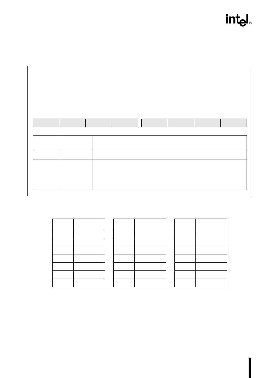
8XC196LX SUPPLEMENT
7.1.3 EPA Interrupt Priority Vector Register
Figure 7-7 illustrates the EPA interrupt priority vector (EPAIPV) register for the 8XC196Lx microcontroller family.
EPAIPV
x
When an EPA
that identifies the highest priority, active, multiplexed interrupt source (see Table 7-2).
EPAIPV allows software to branch via the TIJMP instruction to the correct interrupt service routine
when EPA
the value in EPAIPV. When all the EPA pending bits are cleared, the EPA
7 0
— — — PV4 PV3 PV2 PV1 PV0
Bit
Number
5:7 — Reserved; for compatibility with future devices, write zeros to these bits.
4:0 PV4:0 Priority Vector
interrupt occurs, the EPA interrupt priority vector (EPAIPV) register contains a number
x
is activated. Reading EPAIPV clears the EPA pending bit for the interrupt associated with
Bit
Mnemonic
These bits contain a number from 01H to 14H corresponding to the
highest-priority active interrupt source. This value, when used with the
TIJMP instruction, allows software to branch to the correct interrupt
service routine.
Function
Address:
Reset State:
x
pending bit is also cleared.
1FA8H
00H
Figure 7-7. EPA Interrupt Priority Vector Register (EPAIPV)
Table 7-2. EPA Interrupt Priority Vectors
Value Interrupt Value Interrupt Value Interrupt
14H — 0DH OVR1 06H OVR8
13H — 0CH OVR2 05H OVR9
12H EPA6 0BH OVR3 04H COMP0
11H EPA7 0AH — 03H COMP1
10H EPA8 09H — 02H OVRTM1
0FH EPA9 08H — 01H OVRTM2
0EH OVR0 07H — 00H None
†
87C196LA, LB only; reserved on 83C196LD.
†
†
7-6
Page 65

J1850
Communications
Controller
8
Page 66

Page 67
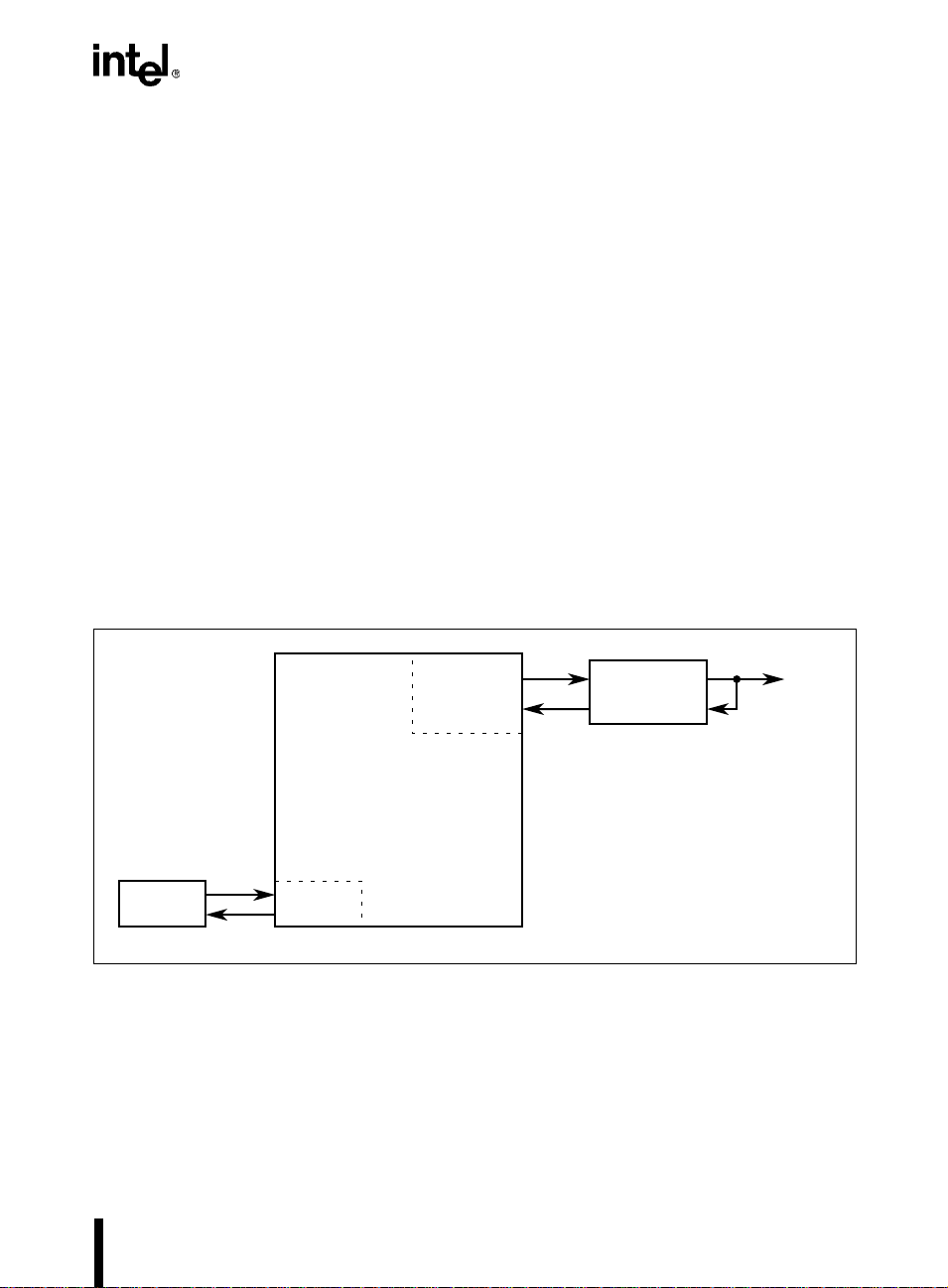
CHAPTER 8
J1850 COMMUNICATIONS CONTROLLER
The J1850 communications controller manages communications between multiple network
nodes. This integrated peripheral supports the 10.4 Kb/s VPW (variable pulse width) mediumspeed class B in-vehicle network protocol. It also supports both the standard and in-frame response (IFR) message framing as specified by the Society of Automotive Engineering (SAE)
J1850 (revised May 1994) techn ical stand ards. Its lower co st per no de makes it suitable f or diagnostics and non-real-time data sharing in applications with high numbers of nodes. This chapter
details the integrated J1850 controller and explains how to configure it.
8.1 J1850 FUNCTIONAL OVERVIEW
The integrated J1850 communications controller transfers messages between network nodes according to the J1850 protocol. The complete J1850 communications protocol solution includes
an on-chip, J1850 digital-logic controller working with an external analog bus transceiver circuit.
Figure 8-1 illustrates the J1850 protocol with the J1850 controller integrated o n the 87C196LB
16-bit microcontroller and a standalone J1850 bus transceiver device. The example uses the Har-
ris HIP7020 as the remote transceiver device.
Clock
TXJ1850
RXJ1850
87C196LB
Microcontroller
PLL/
CLKOUT
Figure 8-1. Integrated J1850 Communications Protocol Solution
TX
RX
HIP7020
The benefit of an integrated, J1850 protocol solution is threefold:
• Minimizes CPU overhead for reception and transmission of J1850 messages.
• Frees up serial and parallel communications ports for other purposes.
• Offers significant printed-circuit board area savings when compared with conventional
standalone protocol devices.
J1850
Bus
A5168-01
8-1
Page 68

8XC196LX SUPPLEMENT
The J1850 controller can handle network protocol functions including message frame sequencing, bit arbitratio n, in- frame re sponse (I FR ) messagi ng, error detecti on, and dela y comp ensatio n.
The J1850 communications controller (Figure 8-2) consists of a control state machine (CSM),
symbol synchronization and timing (SST) circuitry, six control and status registers, transmit and
receive buffers, and an interrupt handler.
J1850ST
J1850RX
J1850TX
OVR
Peripheral Data Bus
Internal Clocking
UNDR
JRX_BUF
Interrupt
Handler
J_DLY
J_STAT
J_TX
JTX_BUF
J_RX
J_CMD
J_CFG
Bus Error
RX
TX
Error
Detection
Circuitry
Bit
Arbitration
Circuitry
Cyclic
Redundancy
Check Circuitry
CSM
J1850 Communications Controller
Delay
Symbol
Encoder
Symbol
Decoder
Prescaler
Compensator
Digital
Filter
SST
TXJ1850
RXJ1850
A5169-01
8-2
Figure 8-2. J1850 Communications Controller Block Diagram
Page 69

J1850 COMMUNICATIONS CONTROLLER
8.2 J1850 CONTROLLER SIGNALS AND REGISTERS
Table 8-1 describes the J1850 contro ller’s pins, and Table 8-2 des cribes the con trol and sta tus
registers.
Table 8-1. J1850 Controller Signals
Signal Type Description
RXJ1850 I Receive
Carries digital symbols from a remote transceiver to the J1850 controller.
TXJ1850 O Transmit
Carries digital symbols from the J1850 controller to a remote transceiver.
Table 8-2. Control and Status Registers
Mnemonic Address Description
J_CFG 1F54H J1850 Configuration
Program this byte register to specify the oscillator prescaler
divisor, mode of operat ion, and normalization bit format. You must
write to this register during the initialization sequence.
J_CMD 1F51H J1850 Command
Program this byte register to specify the number of bytes to be
transmitted in the next message frame. This register also
monitors the status of the message transmission in progress, and
it can abort, ignore, or retry a message if necessary. Read this
register to determine the status of transmissions in progress.
J_DLY 1F58H J1850 Delay Compensation
Program this byte register to define the length of the delay time
through the external transceiver to compensate for the inherent
propagation delays and to accurately resolve bus contention
during arbitration. You must write to this register during the
initialization sequence.
J_RX 1F52H J1850 Receiver
Read this byte register to receive data in byte increments from the
J1850 bus to the microcontroller CPU. This register is buffered to
allow for reception of a second data byte while the first data byte
is being read.
J_STAT 1F53H J1850 Status
Read this byte register to determine the current status of the
receive and transmit buffers and the J1850 interrupt sources. You
can also determine bus status and in-frame response messaging
status. All bits of this register are cleared when read, with the
exception of the BUS_STAT bit.
J_TX 1F50H J1850 Transmitter
Program this byte register to transmit data in byte increments to
the J1850 bus from the microcontroller CPU. This register is
buffered to allow for writing of a second data byte while the first
data byte is being shifted out.
8-3
Page 70

8XC196LX SUPPLEMENT
Table 8-2. Control and Status Registers (Continued)
Mnemonic Address Description
INT_MASK 0008H Interrupt Mask
Bits 6 and 7 in this register enable and disable the J1850 receive
and transmit interrupt requests, respectively.
INT_MASK1 0013H Interrupt Mask 1
Bit 0 in this register enables and disables the J1850 bus error
interrupt request.
INT_PEND 0009H Interrupt Pending
Bits 6 and 7 in this register, when set, indicate pending J1850
receive and transmit interrupt requests, respectively.
INT_PEND1 0012H Interrupt Pending 1
Bit 0 in this register, when set, indicates a pending J1850 bus
error interrupt request.
PTSSEL 0004H PTS Select
Bits 6, 7, and 8 of this word register select either a PTS service
request or a standard interrupt service request for J1850TX,
J1850RX, and J1850ST interrupts, respectively.
PTSSRV 0006H PTS Service
Bits 6, 7, and 8 of this word register are set by hardware to
request an end-of-PTS interrupt for the J1850.
8.3 J1850 CONTROLLER OPERATION
This section describes the control state machine (which contains the cyclic redundancy check
generator) and the symbol synchron ization and timing circuitry fo r J1850 transm issions an d receptions.
8.3.1 Control State Machine
The control state machine (CSM) represents the engine of the digital circuitry portion of the
J1850 communications controller. The CSM handles all message framing for standard and inframe response (IFR) messaging, data validation, bus contention, bit arbitration, and error detection.
8.3.1.1 Cyclic Redundancy Check Generator
The cyclic red undancy ch eck (CRC) generato r circuitry calculate s and checks the CRC byte g en-
erated for both transmitted and received standard messages as specified by SAE J1850 protocol
specification for class B in-vehicle networks. The CRC calculation is a code byte of information
that verifies the proper reception or transmission of yo ur message. Th e calculated CRC code byte
is always appended as the last byte of your transmitted message. On reception, the calculated
CRC checksum byte always results in a value of C4H for valid messages. An inv alid CRC checksum during reception signals the presence of an error in your incoming message, which immediately sets the J1850 bus error (J1850BE) bit in the J_STAT register (Figure 8-19 on page 8-21).
8-4
Page 71

J1850 COMMUNICATIONS CONTROLLER
8.3.1.2 Bus Contention
Bus contention arises when multiple nodes attempt to access and transmit message frames across
the J1850 bus simultaneously. This creates a conflict on the bus. The recognition of conflicting
symbols or bits on th e bus is ref e rred to as contention detection. For example, if a node observes
a difference between a symbol it transmits to the J1850 bus and the symbol that it detects on the
bus, that node has detected contention to the transmission of its message fr ame. Only one message
frame from one node vying for the bus wins arbitration on each symbol or bit of its frame. This
winning message frame does not experience or detect contention. The message frames that were
not awarded arbitration will experience contention.
8.3.1.3 Bit Arbitration
A bit arbitration scheme is used to resolve such conflicts as bus contention. The J1850 protocol
uses the carrier sense multiple access (CSMA) bit arbitration scheme. Bit arbitration is th e process of settling conflicts that occur when multiple nodes attempt to transmit one bit or symbol at
a time across a single bus. A symbol is simply a timing-level formatted bit. By definition, a node
that detects contention has lost arb itration and will discontinue transmitting any further symbols
remaining in its message frame. Remainin g nodes vying for the bus will continu e to send their
symbols until the next in stance of con tention is detected or arbitration is awarded. This p rocess
continues until a complete message frame from one node has been transmitted. For details on this
arbitration scheme, refer to the “Bit Arbitration Example” on page 8-7.
8.3.1.4 Error Detection
The J1850 controller’s error detection logic monitors the bus for four error conditions, and sets
the J1850BE interrupt pending bit in the J_STAT register if an error occurs. The following list
describes each error type:
• CRC error — the calculated CRC checksum received on incoming messages has a value
other than C4H (the expected value for all received message frames).
• bus symbol timing error — the symbol stream on the J1850 bus contains an invalid symbol.
An invalid symbol is any signal that is between 8 µs and 34 µs in duration.
• incomplete byte error — an EOD/EOF symbol occurred,but was not on a byte boundary;
the number of bits recieved was not a multiple of eight.
• no echo — the message is transmitted; however, the transmission’s echo back through the
feedback loop to the receiver has not been detected within the allowable 60 µs window.
8.3.2 Symbol Synchronization and Timing Circuitry
The symbol synchronization and ti ming (SST) circuitry cons ists of a clock prescaler , digital filter ,
delay compensation circu itry, and synch ronization and symbol encoding/ deco ding ci rcuitry . The
SST supports Huntzicker encoding of symbols, which entails 10.4 Kb/s variable pulse-width
(VPW) operation for valid edge detection on message receptions.
8-5
Page 72
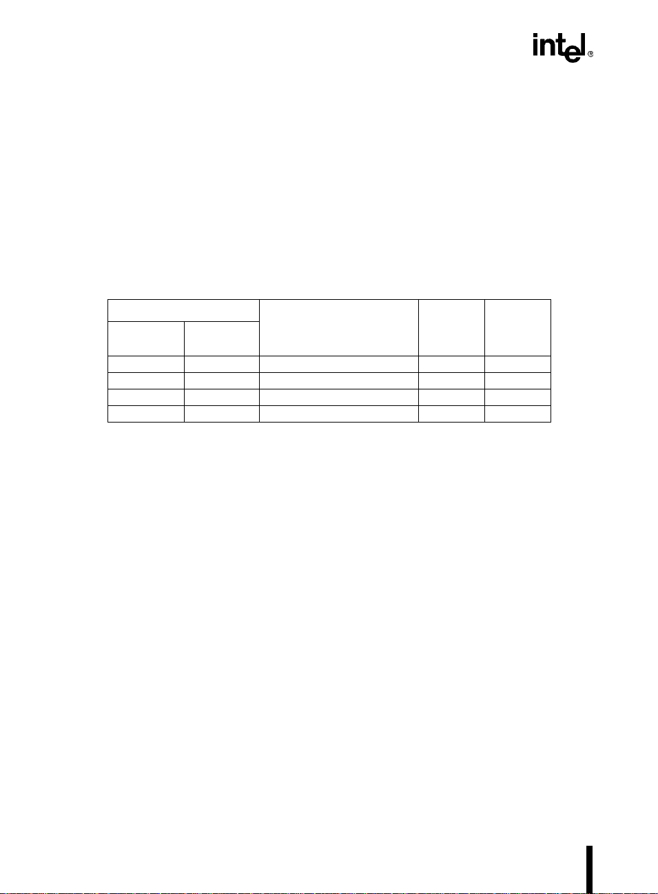
8XC196LX SUPPLEMENT
8.3.2.1 Clock Prescaler
Because the 87C196LB microcontroller can operate at a variety of input freq uencies (F
XTAL
), the
1
clock prescaler circuitry is used to provide a single, internal clock frequency (f/2) to ensure that
the J1850 peripheral is clocked at the proper operating frequency. This is accomplished through
the programmable clock prescaler bits, PRE1:0 in the J_CFG register (Figu re 8-17 on page 8-18).
The prescale bits support input frequencies of 8, 12, 16, and 20 MHz on the XTAL1 pin. With
the phase-locked loop (PLL) cir c uit ry en able d, the prescale bits can support input frequ enci es of
4, 6, 8, and 10 MHz on the XTAL1 pin.
T ab le 8-3 details the relations hips b etween the inp ut fr equen cy, the configuration of PLL, the internal clock frequency, and the prescaler bits.
Table 8-3. Relationships Between Input Frequency, PLL, and Prescaler Bits
F
XTAL1
PLL
Disabled
8 MHz 4 MHz 4 MHz 0 0
12 MHz 6 MHz 6 MHz 0 1
16 MHz 8 MHz 8 MHz 1 0
20 MHz 10 MHz 10 MHz 1 1
8.3.2.2 Digital Filter
PLL
Enabled
Internal Clock Frequency
(f/2)
PRE1 PRE0
T o automatically reject no is e spikes of 8 µs or less in duration, t he J 1850 controller uses a di g ita l
filter between the RXJ1850 input pin and the symbol synchronization logic.
A noise spike is defined as an active or passive state pulse that is shorter in duration than a valid
receive symbol at that state. A valid receive symbol is at least 34 µs in duration. Any symbol captured on the bus between 8 µs and 34 µs in duration is considered invalid and is flagged by the
J_STAT register as a bus-symbol timing error.
8.3.2.3 Delay Compensation
Because the digital portion of the J1850 protocol is integrated onto the microcontroller and physically separated from the transceiver and J1850 bus, control over critical timing parameters of
various manufacturers’ remote transceivers is required. The delay compensation circuitry addresses this requirement by providing the flexib ility to compensate for propagation delay and
pulse-width variations among various transceivers. The compensation circuitry synchronizes itself to the leading edge of each input symbol, which allows for accurate detection of bus contention during bit arbi trat i on. The del ay compensation is programmable thro ugh t he J_DLY register
(Figure 8-18 on page 8-20).
8.3.2.4 Symbol Encoding and Decoding
The J1850 protocol supports the Huntzicker encoding method, which is based on variable pulsewidth (VPW) bus modulat ion. VPW modulati on is a forced high /low symbol trans ition formattin g
scheme that tracks the duration between two consecutive transitions and the level of the bus, active or passive (Figure 8-3).
8-6
Page 73

J1850 COMMUNICATIONS CONTROLLER
1
0
1
0
128µS
"passive 1"
64µS
"passive 0"
1
or
0
1
or
0
64µS
"active 1"
128µS
"active 0"
A5219-01
Figure 8-3. Huntzicker Symbol Definition for J1850
A symbol is defined as a timing-level formatted bit. The VPW symbol timing requirements stipulate that there is one symbol per transition and one transition per symbol. This ensures that a
message frame will always result in a uniform square wavefo rm of v a rying level durations. Figure 8-4 depicts a typical Huntzicker formatted data byte of hex value CCH.
"1"
B7
"1"B5"0"
B6
"1""0"
B4 B3
"1"
B2
"0"
B1
"0"
B0
A5222-01
Figure 8-4. Typical VPW Waveform
Bits 7 and 3 carry logic level 1 data; however, they are represented by a passive-level symbol in
keeping with the VPW requirements. Bits 4 and 0 carry logic level 0 data an d are r epresented b y
an active-level symbol.
8.3.3 Bit Arbitration Example
The drive capacity of each symbol establishes the priority for arbitration. By definition, an active
bus level is a driven state, and a passive bus level is a non -driven, or idle , state. A driven bus state
is always given priority over an idle bus in arbitration. An “active 0” state has priority over an
“active 1” state in arbitration, because the “active 0” state is driven over a longer duration, 128
µs versus the “active 1” state’s drive time of 64 µs. Similarly, a “passive 0” state has priority over
a “passive 1” state, because the “passive 0” state comes out of its idle state in a shorter period of
time, 64 µs versus the “passive 1” state’s idle time of 128 µs.
For example, Figure 8-5 illustrates four node s vyi ng for the bus . Node B is th e first no de to d iscontinue transmitting when it attempts to transmit a “passive 1” symbol onto the bus. At the point
8-7
Page 74

8XC196LX SUPPLEMENT
of arbitration, nodes A, C, and D are all transmitting an “active 0” symbol, thus the idle state of
the “passive 1” symbol is overruled in favor of the driven state of the “active 0” symbol.
Node C is the next node to discontinue transmitting when it attempts to take control of the bus by
transmitting an “active 1” symbol. However, nodes A and D maintain control by continuing to
drive the bus with an “active 0” symbol.
Finally, node D discontinues transmitting when its attempt to hold the bus in an idle state is overruled by the driven state of the “active 1” symbol on node A. Th us, node A is awarded arbitration.
The busline signal, detected on the bus by the receiver, reflects node A’s message, as this is the
only node that did not experience contention.
Node A
Node B
Node C
Node D
Busline
"0" "0" "0" "1""0" "1""0""0"
"0" "0"
"0" "0" "0" "1""0" "1"
"0" "0" "0" "1""0" "1""0"
"1"
Point of
Arbitration
Point of
Arbitration
Point of
Arbitration
A5223-01
Figure 8-5. Bit Arbitration Example
8.4 MESSAGE FRAMES
A message transmission or reception is transferred within a message frame that adds control and
error-detection bits to the content of the message. The frame for an IFR message differs slightly
from that for a standard message, but they contain similar information (Figure 8-6).
8-8
Page 75
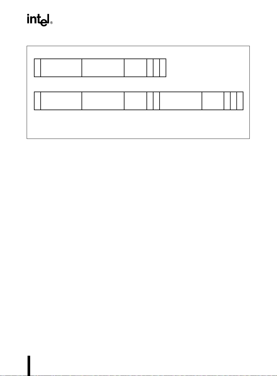
J1850 COMMUNICATIONS CONTROLLER
Standard Frame
E
E
S
1-3 Bytes
O
Header
F
In-frame Response (IFR) Frame
S
1-3 Bytes
O
Header
F
†
The number of data bytes to be transferred is unspecified if 0EH is written to J_CMD3:0.
1-11 Bytes
†
Data
1-11 Bytes
†
Data
1 Byte
CRC
1 Byte
CRC
I
O
O
F
D
F
S
I
E
O
D
1-32 Bytes
N
IFR Data
B
0-1 Byte
CRC
E
O
D
E
F
O
S
F
A5225-01
Figure 8-6. J1850 Message Frames
A standard message frame is initiated by the responder and contains no more than 11 data bytes
to be transmitted. An IFR m e ssage is a request initiating the recipien t(s) to respond by transmitting data within the same frame. The following subsections describe each of the messaging forms.
8.4.1 Standard Messaging
A standard message frame can best be described as a “send mode only” format that is initiated by
the responder either to request inform ation or to reply to a received message fro m a remo te node.
In addition to the actual data that is being transmitted, the standard messag e is composed of a
header (1–3 bytes), a CRC byte, and a series of start and end symbols.
8.4.1.1 Header
The header provides general information o n the p hysical networ k an d the n ecessary interface requirements. For a complete description of the header, refer to the Society of Automotive Engineer-
ing (SAE) J1850 specifications (revised May 1994).
8.4.1.2 CRC Byte
The CRC byte, calculated through the cyclic redundancy check generator, is a checksum value
that verifies the accuracy of the data message transmitted onto the bus. The CRC byte is appended
to all data messages and optionally appended to IFR response messages. Upon reception, the
CRC byte is compared with the value C4H. If the values match, the transmitted message is valid;
otherwise, it is invalid, and an error flag in the J_STAT register is set.
8.4.1.3 Normalization Bit
The normalization bit (NB), found only in IFR messaging, defines the start of the IFR message
response data. The NB is trigger ed by bit J_CMD.6 and is transmitted after an end -of-data (EOD)
symbol is detected on the bus. The timing format of the NB is assigned by the J_CFG register
8-9
Page 76

8XC196LX SUPPLEMENT
(J_CFG.7) and considers whether the IFR message response has a CRC byte appended. Figure
8-7 depicts the SAE preferred, active-level state bit format timing for the NB.
1
0
NB for IFR without CRC
Figure 8-7. Huntzicker Symbol Definition for the Normalization Bit
8.4.1.4 Start and End Message Frame Symbols
64µS
or
1
0
128µS
NB for IFR with CRC
A5220-01
Five symbols are used to mark the start and end of a message frame and to allow the J1850 bus
to properly recognize the interruption of a message transmission or reception. Figure 8-8 illustrates the formats and their respective timing.
The following is a description of each symbol:
• start of frame (SOF) — this symbol signals the start of a message frame. This is an active-
level state symbol only and appears once per frame.
• end of data (EOD) — this symbol signals the end of the data transmission. This is a passive-
level state symbol only. It appears twice in IFR messaging: at the end of the initial request
data field and at the end of the IFR data field.
• end of frame (EOF) — this symbol signals the end of a message frame and returns the bus
to an idle state. This is a passive-level state symbol only. It appears once per frame.
• in-frame separation (IFS) — the timing of this sym bol allo ws for pro per sy nchronization of
multiple nodes during back-to-back transmissions. Nodes contending for the bus must
comply with one of two conditions b e fore transmitting:
— wait for the IFS minimum timing to expire
— wait for a rising edge on the bus after the EOF minimum timing has expired
• break (BRK) — this symbol signals an interruption during a bus transmission. At the point
of termination, all nodes are reset. This is an active-level state sym bol.
8-10
Page 77

J1850 COMMUNICATIONS CONTROLLER
1
0
1
0
1
0
1
0
1
0
200µS
"Start of Frame (SOF)"
200µS
"End of Data (EOD)"
280µS
"End of Frame (EOF)"
300µS+
"In-frame Separation (IFS)"
768µS+
"Break Signal (BRK)"
Figure 8-8. Definition for Start and End of Frame Symbols
Table 8-4 details the symbol timing characteristics supported by the 87C196LB.
A5221-01
Table 8-4. Huntzicker Symbol Timing Characteristics
Name Symbol Bus Level TTXmin TTXnom TTXmax TRXmin TRXmax Units
Logic Level 0 0
Logic Level 1 1
Start of Frame SOF Active 193 200 207 163 <239 µs
End of Data EOD Passive 193 200 207 163 <239 µs
End of Frame EOF Passive 271 280 289 239 <300 µs
In-frame Separation IFS Passive >300 — — >300 — µs
Break BRK Active 768 — — >239 — µs
NOTE: Timings are based on the standard bus rate of 10.4 Kb/s. When operating in 4x mode, the bus
rate becomes 41.6 Kb/s and all symbol timings are one fourth that shown.
Passive 60 64 68 34 <96 µs
Active 122 128 134 96 <163 µs
Passive 122 128 134 96 <163 µs
Active 60 64 68 34 <96 µs
8-11
Page 78

8XC196LX SUPPLEMENT
8.4.2 In-frame Response Messaging
There are three types of in-frame response (IFR) message framings: type 1 (a single byte from a
single responder), type 2 (a single byte from multiple responders), and type 3 (multiple bytes from
a single responder). Like the standard m essage frame, the IFR frame is composed of header , data,
and CRC bytes, and a series of start and end symbols. Unlike the standard message frame, the
actual length of the IFR message frame will differ based on the desired respons e.
Consider the following example: a system’s controller (the requestor) requests an information update from each of four nodes (the responders) in the system. W ith type 1 messaging, the controller
can receive a limited information update if it sends out four separate transmissions. With type 2
messaging, the controller can receive a limited info rmation update by sending one message. W ith
type 3 messaging, the controller can receive unlimited information; however, it will require four
separate transmissions. The following subsections detail this example for the three IFR messaging types.
8.4.2.1 IFR Messaging Type 1: Single Byte, Single Responder
No IFR messaging type carries a distinct advantage or disadvantage over the other messaging
types. IFR messaging type 1 (Figure 8-9) is ideal for use when requesting small amounts of information from a single source in your system. In the above example, suppose you want to know
how many pounds of pressure each of the fou r remote nod e sites exper ienced after the controller
sent out a request to each node sensor to exert a given amount of pr essure. If y ou use type 1 messaging, the controller will send four separat e serial messages to the remote node sites in the system and wait for their responses. Keeping the data timing a constant, the CPU overhead of
transmitting these messages alone amounts to a minimum of 4.96 ms (refer to Table 8-4 on page
8-11 for all symbol timings).
In-frame Response (IFR) Frame
S
1-3 Bytes
O
Header
F
†
The number of data bytes to be transferred is unspecified if 0EH is written to J_CMD3:0.
1-11 Bytes
†
Data
1 Byte
CRC
E
1Byte
N
O
IFR Data
B
D
0-1 Byte
CRC
E
E
I
O
O
F
D
F
S
A5229-01
Figure 8-9. IFR Type 1 Message Frame
8.4.2.2 IFR Messaging Type 2: Single Byte, Multiple Responders
When response time is the highest consideration, IFR messaging type 2 is desirable. IFR type 2
messaging can monitor up to 32 remote nodes on a given request (see Figure 8-10). While it allows only one byte of information per response, in many cases a single byte of information is
more than adequate. In our example, suppose that each node sensor detected a pressure of 75
P.S.I. (pounds per square inch). The response (the value 75) would take a single byte, 46H, to
communicate the reply. The maximum overhead required is 1.24 ms, or one fourth the time it
would take type 1 messaging to achieve the same results.
8-12
Page 79

J1850 COMMUNICATIONS CONTROLLER
††
E
E
D
31
0-1 Byte
CRC
O
D
I
O
F
F
S
A5227-01
N
0
B
IFR Data Field
. . . . . . . . . .
D1D
In-frame Response (IFR) Frame
S
1-3 Bytes
O
Header
F
†
The number of data bytes to be transferred is unspecified if 0EH is written to J_CMD3:0.
††
block in the IFR data field represents a byte of data from a different remote node.
Each D
X
1-11 Bytes
†
Data
1 Byte
CRC
E
O
D
Figure 8-10. IFR Type 2 Message Frame
8.4.2.3 IFR Messaging Type 3: Multiple Bytes, Single Responder
IFR messaging type 3 (Figure 8-11) is ideal for requesting large amounts of information from a
single source in your system. You can compile up to 12 bytes of data from a remote node on a
single request. In our example, for the same amount of CPU overhead as IFR type 1 messaging
exhausted (4.96 ms), you can gather up to twelve times as much information.
In-frame Response (IFR) Frame
S
1-3 Bytes
O
Header
F
†
The number of data bytes to be transferred is unspecified if 0EH is written to J_CMD3:0.
1-11 Bytes
†
Data
1 Byte
CRC
E
O
D
1-12 Bytes
N
IFR Data
B
0-1 Byte
CRC
E
O
D
E
I
O
F
F
S
A5228-01
Figure 8-11. IFR Type 3 Message Frame
8.5 TRANSMITTING AND RECEIVING MESSAGES
The J1850 controller can transmit and receive messages in either standard or IFR form.
8.5.1 Transmitting Messages
To transmit a standard message, prepare the message in register RAM and then write it to the
J1850 transmit (J_TX) register (Figure 8-12) one byte at a time.
8-13
Page 80

8XC196LX SUPPLEMENT
J_TX
The J1850 transmitter (J_TX) register transfers data in byte increments to the J1850 bus from the
microcontroller CPU. This register is buffered to allow for transmission of a second data byte while the
first data byte is being shifted out. This byte register can be read or written, and is addressable
windowing
through
7 0
.
Address:
Reset State:
1F50H
00H
Transmit Byte
Bit
Number
7:0 DB7:0 Data Bits
Bit
Mnemonic
Function
These eight bits compose the data byte to be transmitted to the J1850 bus.
Figure 8-12. J1850 Transmitter (J_TX) Register
Transmitting the message requires that you first program the J1850 command (J_CMD) register
to specify the number of bytes you want to transfer across the J1850 bus. The number of bytes
specified must include the header byte(s). After the start of frame (SOF) symbol is put on the bus,
the first header byte is transferred to J_TX for transmission. This byte will automatically be transferred into the J1850 transmit buffer (JTX_BUF) and the second byte of the mess age frame will
be written to J_TX. The transfer of the first byte to JTX_BUF triggers the transm ission process
and generates the J1850 trans missi on (J1 850T X) int errupt (if it is en abled), s ignalin g that J_TX
is available for another byte (Figure 8-13).
CPU
J_TX
JTX_BUF
Message transmit
interrupt (J1850TX) set
J1850 Bus
A5235-01
Figure 8-13. J1850 Transmit Message Structure
After the byte in JTX_BUF is transmitted, the byte residing in J_TX is automatically shifted into
JTX_BUF, freeing J_TX for another byte. This process cont inues un til th e CSM has res olved the
number of message bytes (MSG3:0) programmed into the J_CMD register.
If the last message byte being transmitted is shifted out before the MSGx count expires, a
J1850ST core interrupt is generated and the OVR_UNDR (J_STAT.3) bit records a transmitter
underflow error in the J_STAT register.
8-14
Page 81
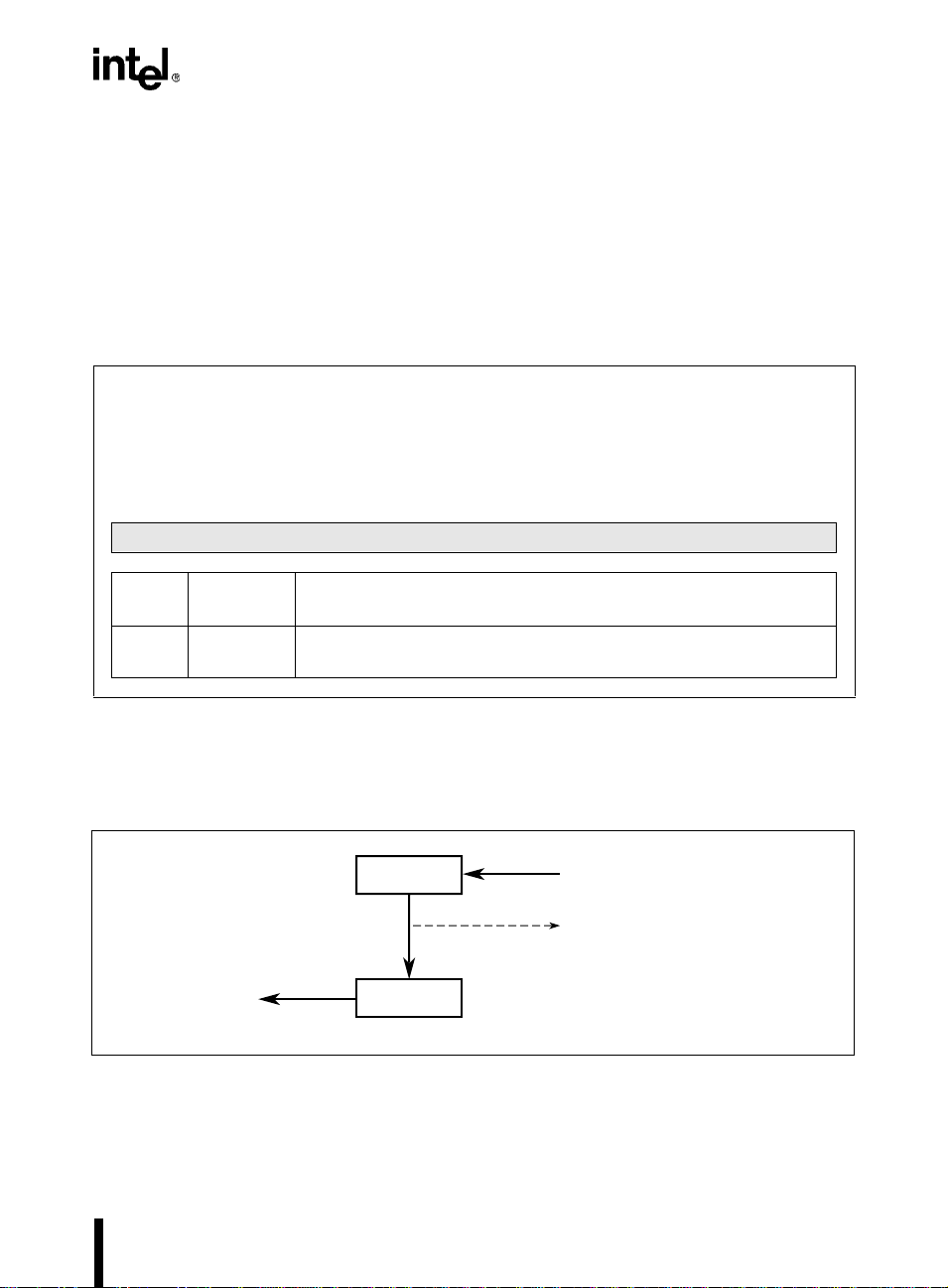
J1850 COMMUNICATIONS CONTROLLER
NOTE
An overrun condition can occur on transmission if the transmit buffer,
JTX_BUF, is overwritten.
8.5.2 Receiving Messages
For a message reception, after a SOF is detected on th e bus, the controller star ts to shift data symbols into the J1850 receive buffer (JRX_BUF) until an entire data byte has been received. This
byte is automatically transferred into the J185 0 receive (J_RX) r egister (Figure 8-14) and the subsequent byte is written into the empty JRX_BUF.
J_RX
The J1850 receiver (J_RX) register transfers received data in byte increments from the J1850 bus to
the microcontroller CPU. This register is buffered to allow for reception of a second data byte while
the first data byte is being read. This byte register can be read or written, and is addressable through
windowing
7 0
.
Address:
Reset State:
1F52H
00H
Receive Byte
Bit
Number
7:0 DB7:0 Data Bits
Bit
Mnemonic
Function
These eight bits compose the last data byte received from the J1850 bus.
Figure 8-14. J1850 Receiver (J_RX) Register
The transfer of the first byte to J_RX triggers the reception process and generates the J1850 reception (J1850RX) interrupt (if it is enabled), sign aling that JRX_BUF is available for an other
byte (Figure 8-15).
JRX_BUF
J1850 Bus
Message receive
interrupt (J1850RX) set
CPU
J_RX
A5236-01
Figure 8-15. J1850 Receive Message Structure
After J_RX is read, the byte residing in JRX_BUF is automatically shifted into J_RX, freeing
JRX_BUF for another reception. This process continues until an end of data (EOD) symbol is encountered.
8-15
Page 82

8XC196LX SUPPLEMENT
If a third byte is received before J_RX is read, a J1850ST core interrupt is generated and the
OVR_UNDR (J_STAT.3) bit records a receiver overrun error in the J_STAT register.
8.5.3 IFR Messages
In-frame response (IFR) messaging is identical in setup to standard messaging for both transmission and reception. It uses the same registers to configure, communicate, and control data. The
difference is that the requestor initiating the IFR message sequen ce writes the message specifying
a response from either one or more nodes in the system. Framing a message in this manner bypasses needless CPU overhead that can result from lengthy EOF symbols, and it gives you a faster
response to the information you are accessing from remote sites in your system. (Refer to “In-
frame Response Messaging” on page 8-12 for a detailed explanation).
8.6 PROGRAMMING THE J1850 CONTROLLER
This section explains how to configure the J1850 controller. Several registers combine to control
the configuration: the command register, the configuration register, the delay compensation register, and the status register.
Programming the J1850 controller requires that you first program the configuration and delay
registers during initialization. You need to program these two registers only once per initialization sequence.
After initialization, you must first program the command register, followed by either the receive
or transmit register, and then the status register.
8.6.1 Programming the J1850 Command (J_CMD) Register
The J1850 command register (Figure 8-1 6) d etermines the messag ing ty pe, specifies the num ber
of bytes to be transmitted in the next message frame, and updates the status of the messag e transmission in progress.
8-16
Page 83

J1850 COMMUNICATIONS CONTROLLER
J_CMD
The J1850 command (J_CMD) register determines the messaging type, specifies the number of bytes
to be transmitted in the next message frame, and updates the status of the message transmission in
progress. This byte register can be directly addressed through
register prior to transmitting every message.
7 0
AUTO IFR IGNORE ABORT MSG3 MSG2 MSG1 MSG0
Bit
Number
7 AUTO Automatic Transmit Retry
6 IFR In-frame Response Indicator
5 IGNORE Ignore Incoming Message
4 ABO RT Ab ort Transmission
3:0 MSG3:0 Message
Bit
Mnemonic
This bit, when arbitration is lost on the first byte of your message, prompts
the transmitter to automatically retry until the byte is successfully
transmitted. Automatic retry applies only to the first byte.
0 = normal operation
1 = enable automatic retry
This bit signals that a normalization bit (NB) is to be sent after an end-ofdata symbol is detected on the bus and that the subsequent byte written to
the J1850 transmitter (J_TX) register is an in-frame response (IFR).
0 = standard messaging
1 = next byte written to J_TX is an IFR
This bit instructs the bus to ignore the incoming message until an EOF
symbol is detected. The bit is cleared after an EOF symbol is detected.
0 = normal operation
1 = ignore incoming message
This bit aborts any transmission in progress and flushes the transmit buffer
(JTX_BUF). To prevent another node from mistakenly assuming that the
last byte was a CRC byte, two extra ‘1’s are appended.
0 = normal operation
1 = abort transmission in progress
These four bits specify the number of bytes to be transmitted in the next
message frame. This number includes the header, but not the CRC byte. In
normal messaging, the maximum number of bytes you can transmit in a
message frame is eleven.
MSG3:0 Operation Purpose
FH Termination byte Terminate block transmission
EH Block transmission Transmit unspecified number of bytes
DH Reserved —
CH Reserved —
B:0H Normal messaging Transmit specified number of bytes
windowing
Function
Address:
Reset State:
. You must write to this
1F51H
00H
Figure 8-16. J1850 Command (J_CMD) Register
8-17
Page 84

8XC196LX SUPPLEMENT
8.6.2 Programming the J1850 Configuration (J_CFG) Register
The J1850 configuration register (Figure 8-17) selects th e proper os cillator prescaler, initiates a
transmission break for debugging, invokes clock quadrupling operation, and selects the normalization bit format.
J_CFG
The J1850 configuration (J_CFG) register selects the proper oscilator prescaler, initiates transmission
break for debug, invokes clock quadrupling operation, and selects the normalizartion bit format. This
byte register can be directly addressed through
first write to this register.
7 0
NBF IFR3 4XM TXBRK RXPOL — PRE1 PRE0
Bit
Number
7 NB F Normalization Bit Format
6 IFR3 Type 3 IFR Messaging
5 4X M Oscillator Quadruple (4x) Mod e
4 T XB RK Transmission Break
3 RX POL Receive Polarity
Bit
Mnemonic
This bit specifies which normalization bit (NB) format is to be used.
IFR with CRC Byte IFR without CRC Byte
0 = active long NB 0 = active short NB
1 = active short NB 1 = active long NB
This bit selects type 3 IFR messaging, which supports the in-frame transfer
of an unspecified number of data bytes.
0 = normal operation
1 = type 3 IFR messaging
This bit allows the J1850 peripheral to operate at four times the normal bit
transfer rate (41.6 Kb/s versus 10.4 Kb/s).
0 = normal operation
1 = 4x mode operation
This bit will terminate any transmission in progress by writing a break (BRK)
symbol to the bus.
0 = normal operation
1 = transmit BRK symbol onto bus
This bit changes the polarity of the receive symbol.
0 = normal operation – Rx input inverted
1 = receive polarity enabled – Rx input non-inverted
windowing
. All J1850 bus activity is ignored until you
Function
Address:
Reset State:
1F54H
00H
8-18
Figure 8-17. J1850 Configuration (J_CFG) Register
Page 85

J1850 COMMUNICATIONS CONTROLLER
J_CFG
The J1850 configuration (J_CFG) register selects the proper oscilator prescaler, initiates transmission
break for debug, invokes clock quadrupling operation, and selects the normalizartion bit format. This
byte register can be directly addressed through
first write to this register.
7 0
NBF IFR3 4XM TXBRK RXPOL — PRE1 PRE0
Bit
Number
2 — Reserved; for compatibility with future devices, write zero to this bit.
1:0 PRE1:0 J1850 Oscillator Prescaler
Bit
Mnemonic
These bits ensure proper operation of the J1850 peripheral at the supported
input frequencies (F
PRE1 PRE0 F
00 8 MHz
0 1 12 MHz
1 0 16 MHz
1 1 20 MHz
windowing
).
XTAL1
XTAL1
. All J1850 bus activity is ignored until you
Function
Address:
Reset State:
1F54H
00H
Figure 8-17. J1850 Configuration (J_CFG) Register (Continued)
8.6.3 Programming the J1850 Delay Compensation (J_DLY) Register
The J1850 delay compensation register (Figur e 8-1 8) allows y ou to pro gram the n ecessary delay
time through the external transceiver to compensate for the inherent propagation delays and to
accurately resolve bus contention during arbitration.
8-19
Page 86
8XC196LX SUPPLEMENT
J_DLY
The J1850 delay (J_DLY) register allows you compensate for the inherent propagation delays and to
accurately resolve bus contention during arbitration. This byte register can be directly addressed
windowing
through
7 0
— — — DLY4 DLY3 DLY2 DLY1 DLY0
Bit
Number
7:5 — Re served; for compatibility with future devices, write zeros to these bits.
4:0 DLY4:0 Delay Time
.
Bit
Mnemonic
Function
These five bits specify the desired propagation delay between the J1850
controller circuitry and the off-chip transceiver device, in units of
microseconds (µs).
Address:
Reset State:
1F58H
00H
Figure 8-18. J1850 Delay (J_DLY) Register
8-20
Page 87

J1850 COMMUNICATIONS CONTROLLER
8.6.4 Programming the J1850 Status (J_STAT) Register
The J1850 status register (Figure 8-19) provides the current status of the message and the four
interrupt sources associated with the J1850 protocol.
J_STAT
The J1850 status (J_STAT) register provides the current status of the message transfer, the receive
and transmit buffers, and the four interrupt sources associated with the J1850 protocol. This byte
register can be directly addressed through
transmitting each message. Reading this register clears all bits except BUS_STAT.
7 0
IFR_RCV BUS_CONT BUS_STAT BRK_RCV OVR_UNDR MSG_TX MSG_RX J1850BE
Bit
Number
7 IFR_RC V In-frame Response Received
6 BUS_CONT J1850 Bus Contention
5 BUS_STAT J1850 Bus Status
4 BR K_RCV Break Received
3 OVR_UNDR Receive Overrun/Transmit Underflow Interrupt
Bit
Mnemonic
This bit indicates whether the IFR byte has been received and is ready to
be read from the J1850 receiver (J_RX) register.
0 = no action
1 = IFR byte received
This bit indicates whether bus contention has been detected and arbitration
has been lost.
0 = no action
1 = bus contention
This bit indicates whether a transmission or reception is in progress on the
J1850 bus.
0 = J1850 bus idle
1 = J1850 bus busy
This bit indicates whether a BRK symbol has been detected on the J1850
bus.
0 = no action
1 = BRK symbol detected
This bit indicates whether a receive buffer overrun (OVR) or transmit buffer
underflow (UNDR) has occurred. An overrun occurs when a symbol is
received while both J_RX and JRX_BUF contain unread bytes. An
underflow occurs when a transmission is attempted while both J_TX and
JTX_BUF are empty.
0 = normal operation
1 = OVR or UNDR detected
windowing
. You must write to this register before
Function
Address:
Reset State:
1F53H
00H
Figure 8-19. J1850 Status (J_STAT) Register
8-21
Page 88

8XC196LX SUPPLEMENT
J_STAT
The J1850 status (J_STAT) register provides the current status of the message transfer, the receive
and transmit buffers, and the four interrupt sources associated with the J1850 protocol. This byte
register can be directly addressed through
transmitting each message. Reading this register clears all bits except BUS_STAT.
7 0
IFR_RCV BUS_CONT BUS_STAT BRK_RCV OVR_UNDR MSG_TX MSG_RX J1850BE
Bit
Number
2 MSG_TX Message Transmit Interrupt
1 MSG_RX Message Receive Interrupt
0 J1850BE J1850 Bus Error Interrupt
Bit
Mnemonic
This bit signals the successful transmission of a message upon detecting
the EOD symbol.
0 = no action
1 = message transmitted
This bit signals the successful reception of a message upon detecting the
EOD symbol.
0 = no action
1 = message received
This bit is set if one or more of the following conditions occur:
• the calculated CRC for a received message does not equal C4H
• an incomplete byte is received on the bus
• an invalid bus symbol is detected on the bus
• a transmission occurs and the feedback through the receiver is not
detected within 60 µs
windowing
. You must write to this register before
Function
Address:
Reset State:
1F53H
00H
8-22
Figure 8-19. J1850 Status (J_STAT) Register (Continued)
Page 89

Minimum Hardware
Considerations
9
Page 90

Page 91
CHAPTER 9
MINIMUM HARDWARE CONSIDERATIONS
This chapter discusses the major hardware consideration differences between the 8XC196Lx and
the 8XC196Kx. The 8XC196Lx has implemented a reset source SFR that reveals the source of
the most recent reset request.
9.1 IDENTIFYING THE RESET SOURCE
The reset source (RSTSRC) register indicates the source of the last reset that the m icrocon troller
encountered (Figure 9-1). If more than one reset occurs at the same time, all of the corr esponding
RSTSRC bits are set. Reading this SFR clears all the register bits.
RSTSRC
The reset source (RSTSRC) register indicates the source(s) of the last reset that the microcontroller
encountered.
7 0
— — — — CFDRST WDTRST SFWRST EXTRST
Bit
Number
7:4 — Reserved; for compatibility with future devices, write zeros to these bits.
3 CFDRST Clock Failure Detection Reset
2 WDTRST Watchdog Timer Reset
1 SFWRST Software Reset
0 EXTRST External Reset
NOTE:
1. The State of the RSTSRC register is inderterminate on a V
states will have the corresponding reset event bit set in the register.
Bit
Mnemonic
Function
When set, this bit indicates that a failed clock caused the last reset.
When set, this bit indicates that the watchdog timer caused the last reset.
When set, this bit indicates that either the RST instruction or the IDLPD
instruction used with an illegal key caused the last reset.
When set, this bit indicates that the RESET# pin being asserted caused the
last reset.
power up condition. All other reset
CC
Address:
Reset State:
1F92H
XXH
Figure 9-1. Reset Source (RSTSRC) Register
(1)
9-1
Page 92

8XC196LX SUPPLEMENT
9.2 DESIGN CONSIDERATIONS FOR 8XC196LA, LB, AND LD
With the exception of a few new multiplexed functions, the 8XC196Lx microcontrollers are pin
compatible with the 8XC1 96Jx microcontrollers . The 8XC196Jx microcontrollers are 52-lead
versions of 8XC196Kx microcontrollers.
Follow these recommendations to hel p maintain hardware and software compatibility between
the 8XC196Lx, 8XC196Kx, and future microcontrollers.
• Bus width. Since the 8XC196Lx has neither a WRH# nor a BUSWIDTH pin, the
microcontroller cannot dynamically switch between 8- and 16-bit bus widths. Program the
CCBs to select 8-bit bus mode.
• Wait states. Since the 8XC196Lx has no READY pin, the microcont ro l ler cannot rely on a
READY signal to control wait states. Program the CCBs to limi t the number of wait states
(0, 1, 2, or 3).
• EPA6–EPA7. These functions exist in the 8XC196Lx, but the associated pins are omitted.
You can use these functions as software timers, to start A/D conversions (on 87C196LA
and LB only), or to reset the timers.
• Slave port. Since the 8XC196Lx has no P5.1/SLPCS and P5.4/SLPINT pins, you cannot
use the slave port.
• ONCE mode. On the 8XC196Lx, the ONCE mode entry function is multiplexed with P2.6
(and TXJ1850 on the 87C196LB) rather than with P5.4 as it is on the 8XC196Kx
(P5.4/SLPINT/ONCE).
• NMI. Since the 8XC196Lx has no NMI pin, the nonmaskable interrupt is not supported.
Initialize the NMI vector (at location 203EH) to point to a RET instructi on. This method
provides glitch protection only.
• I/O ports. The following port pins do not exist in the 8XC196Lx: P0.0–P0.1, P1.4–P1.7,
P2.3 and P2.5, P5.1 and P5.4–P5.7, P6.2 and P6.3. Software can still read and write the
associated Px_REG, Px_MODE, and Px_DIR registers. Configure the registers for the
omitted pins as f ollows:
— Clear the corresponding Px_DIR bits. (Configures pins as complementary outputs.)
— Clear the corresponding Px_MODE bits. (Selects I/O port function.)
— Write either “0” or “1” to the corresponding P x_REG bits. (Effectively ties signals low
or high.)
Do not use the bits associated with the omitted port pins for conditional branch instructions.
Treat these bits as reserved.
• Auto programming. During auto programming, the 8XC196Lx supports only a 16-bit,
zero-wait-state bus configuration.
9-2
Page 93

Special Operating
Modes
10
Page 94

Page 95

CHAPTER 10
SPECIAL OPERATING MODES
The 8XC196Lx’s idle and powerdown modes are the same as those of the 8XC1 96Kx. However,
the clock circuitry has changed, and the on-circuit emulation (ONCE) special-purpose mode operation has changed slightly because of the new reset state pin levels that have been implemented.
10.1 INTERNAL TIMING
The 87C196LA and LB clock circuitry (Figure 10-1) implements a phase-locked loop and clock
multiplier circuitry, which can substantially increase the CPU clock rate while using a lower-frequency input clock.
10-1
Page 96

8XC196LX SUPPLEMENT
XTAL1
XTAL2
F
XTAL1
Disable Oscillator
(Powerdown)
XTAL1
F
Disable
PLL
(Powerdown)
PLLEN
XTAL1
1
2F
0
Divide by two
Circuit
Clock
Generators
Programmable
Divider
(CLK1:0)
Phase
Comparator
Phase-locked
Oscillator
Phase-locked Loop
Clock Multiplier
f
Disable Clock Input (Powerdown)
f/2
Clock
Failure
Detection
f/2
Filter
To reset logic
Disable Clocks (Idle, Powerdown)
CPU Clocks (PH1, PH2)
Peripheral Clocks (PH1, PH2)
OSC
0
CLKOUT
1
Disable Clocks (Powerdown)
A5290-01
Figure 10-1. Clock Circuitry (87C196LA, LB Only)
10.2 ENTERING AND EXITING ONCE MODE
ONCE mode isolates the device from other components in the system to allow printed-circuitboard testing or debugg ing with a clip-on em ulator. During ONCE mode, all pins except XTAL1,
XTAL2, V
, and VCC are weakly pulled either high or low. During ONCE mode, RESET# must
SS
be held high or the device will exit ONCE mode and enter the reset state.
On the 87C196LA and LB, the reset state level of all 41 general-purpose I/O pins has changed
from a weak logic “1” (wk1) to a weak logic “0” (wk0). ONCE shares a package with port pin
2.6. Asserting and holding the ONCE signal high during the rising edge of RESET# causes the
device to enter ONCE mode. To prevent accidental entry into ONCE mode, configure this pin as
10-2
Page 97

SPECIAL OPERATING MODES
an output. If you cho os e t o conf igure this pin as an input , al ways hol d i t l ow d uri n g r e set and ensure that your system meets the V
specification to prevent inadvertent entry into ONCE mode.
IH
10-3
Page 98

Page 99

Programming the
Nonvolatile Memory
11
Page 100

 Loading...