

Page 1

R
Intel® 855PM Chipset Platform
Design Guide
For use with Intel® Pentium® M and Intel® Celeron® M Processors
May 2004
Revision Number 003
Document Number: 252614-003
Page 2

R
Information in this document is provided in connection with Intel products. No license, express or implied, by estoppel or otherwise, to any intellectual
property rights is granted by this document. Except as provided in Intel’s Terms and Conditions of Sale for such products, Intel assumes no liability
whatsoever, and Intel disclaims any express or implied warranty, relating to sale and/or use of Intel products including liability or warranties relating to
fitness for a particular purpose, merchantability, or infringement of any patent, copyright or other intellectual property right. Intel products are not intended
for use in medical, life saving, or life sustaining applications.
Actual system-level properties, such as skin temperature, are a function of various factors, including component placement, component power
characteristics, system power and thermal management techniques, software application usage and general system design. Intel is not responsible for its
customers’ system designs, nor is Intel responsible for ensuring that its customers’ products comply with all applicable laws and regulations. Intel
provides this and other thermal design information for informational purposes only. System design is the sole responsibility of Intel’s customers, and
Intel’s customers should not rely on any Intel-provided information as either an endorsement or recommendation of any particular system design
characteristics.
Intel may make changes to specifications and product descriptions at any time, without notice.
Designers must not rely on the absence or characteristics of any features or instructions marked "reserved" or "undefined." Intel reserves these for future
definition and shall have no responsibility whatsoever for conflicts or incompatibilities arising from future changes to them.
The Intel® Pentium® M processor, Intel® Pentium® M processor on 90nm process with 2-MB L2 Cache, Intel® Celeron® M Processor and Intel® 855PM
Chipset may contain design defects or errors known as errata which may cause the product to deviate from published specifications. Current
characterized errata are available on request.
Contact your local Intel sales office or your distributor to obtain the latest specifications and before placing your product order.
Alert on LAN is a result of the Intel-IBM Advanced Manageability Alliance and a trademark of IBM.
Copies of documents which have an ordering number and are referenced in this document, or other Intel literature, may be obtained from:
Intel Corporation
www.intel.com
or call 1-800-548-4725
Intel, the Intel logo, Pentium, Celeron, Intel SpeedStep, and Intel Centrino are trademarks or registered trademarks of Intel Corporation and its
subsidiaries in the United States and other countries.
*Other brands and names are the property of their respective owners.
2 Intel
®
855PM Chipset Platform Design Guide
Page 3

R
Contents
1.
2.
3.
4.
Introduction .................................................................................................................................19
1.1. Terminology ...................................................................................................................19
1.2. Referenced Documents .................................................................................................21
System Overview........................................................................................................................23
2.1. Intel® CentrinoTM Mobile Technology Features..............................................................23
2.2. Intel® Pentium® M Processor/Intel® Celeron® M Processor ............................................25
2.2.1. Architectural Features ....................................................................................25
2.2.1.1. Packaging/Power ............................................................................25
2.3. Intel 855PM Memory Controller Hub (MCH)..................................................................25
2.3.1. Front Side Bus Support..................................................................................25
2.3.2. Integrated System Memory DRAM Controller................................................26
2.3.3. Accelerated Graphics Port (AGP) Interface...................................................26
2.3.4. Packaging/Power ...........................................................................................26
2.4. Intel 82801DBM I/O Controller Hub (ICH4-M) ...............................................................27
2.4.1. Packaging/Power ...........................................................................................27
2.5. Intel PRO/Wireless Network Connection.......................................................................27
2.5.1. Packaging and Power ....................................................................................28
2.6. Firmware Hub (FWH).....................................................................................................28
2.6.1. Packaging/Power ...........................................................................................28
General Design Considerations .................................................................................................29
3.1. Nominal Board Stack-Up ...............................................................................................29
FSB Design Guidelines ..............................................................................................................33
4.1. FSB Design Recommendations.....................................................................................33
4.1.1. Recommended Stack-up Routing and Spacing Assumptions .......................33
4.1.1.1. Trace Space to Trace – Reference Plane Separation Ratio ..........33
4.1.1.2. Trace Space to Trace Width Ratio..................................................34
4.1.1.3. Recommended Stack-up Calculated Coupling Model ....................34
4.1.1.4. Signal Propagation Time to Distance Relationship
and Assumptions.............................................................................35
4.1.2. Common Clock Signals..................................................................................36
4.1.3. Source Synchronous Signals.........................................................................41
4.1.3.1. Source Synchronous General Routing Guidelines .........................41
4.1.3.2. Source Synchronous – Data ...........................................................43
4.1.3.3. Source Synchronous – Address .....................................................44
4.1.3.4. Source Synchronous Signals Recommended Layout Example .....45
4.1.3.5. Trace Length Equalization Procedures...........................................50
4.1.4. Asynchronous Signals....................................................................................51
4.1.4.1. Topologies.......................................................................................51
4.1.4.1.1. Topology 1A: Open Drain (OD) Signal Driven by the
Processor – IERR# .......................................................52
4.1.4.1.2. Topology 1B: Open Drain (OD) Signals Driven by the
Processor – FERR# and THERMTRIP#.......................53
4.1.4.1.3. Topology 1C: Open Drain (OD) Signals Driven by the
Processor – PROCHOT#..............................................54
4.1.4.1.4. Topology 2A: Open Drain (OD) Signal Driven by Intel
82801DBM ICH4-M – PWRGOOD ...............................55
4.1.4.1.5. Topology 2B: CMOS Signals Driven by Intel 82801DBM
ICH4-M – DPSLP#........................................................56
®
Intel
855PM Chipset Platform Design Guide 3
Page 4

5.
R
4.1.4.1.6.
4.1.4.1.7. Topology 3: CMOS Signals Driven by Intel 82801DBM
4.1.4.2. Voltage Translation Logic ............................................................... 60
4.1.5. Processor RESET# Signal ............................................................................ 60
4.1.5.1. Processor RESET# Routing Example............................................ 62
4.1.6. Processor and Intel 855PM MCH Host Clock Signals .................................. 63
4.1.7. GTLREF Layout and Routing Recommendations ......................................... 65
4.1.8. AGTL+ I/O Buffer Compensation .................................................................. 69
4.1.8.1. Processor AGTL+ I/O Buffer Compensation ..................................69
4.1.8.2. Intel 855PM MCH AGTL+ I/O Buffer Compensation...................... 71
4.1.9. Processor FSB Strapping .............................................................................. 73
4.1.10. Processor V
4.2. Intel System Validation Debug Support ........................................................................ 76
4.2.1. In Target Probe (ITP) Support ....................................................................... 76
4.2.1.1. Background and Justification ......................................................... 76
4.2.1.2. Implementation ............................................................................... 76
4.2.2. Processor Logic Analyzer Support (FSB LAI) ............................................... 76
4.2.2.1. Background and Justification ......................................................... 76
4.2.2.2. Implementation ............................................................................... 77
4.2.3. Intel Pentium M Processor and Intel Celeron M Processor On-Die Logic
Analyzer Trigger Support (ODLAT) ............................................................... 77
4.3. Onboard Debug Port Routing Guidelines ..................................................................... 77
4.3.1. Recommended Onboard ITP700FLEX Implementation................................ 78
4.3.1.1. ITP Signal Routing Guidelines........................................................ 78
4.3.1.2. ITP Signal Routing Example........................................................... 82
4.3.1.3. ITP_CLK Routing to ITP700FLEX Connector ................................ 83
4.3.1.4. ITP700FLEX Design Guidelines for Production Systems .............. 85
4.3.2. Recommended ITP Interposer Debug Port Implementation ......................... 86
4.3.2.1. ITP_CLK Routing to ITP Interposer................................................ 86
4.3.2.2. ITP Interposer Design Guidelines for Production Systems ............ 87
4.3.3. Logic Analyzer Interface (LAI) ....................................................................... 87
4.3.3.1. Mechanical Considerations ............................................................88
4.3.3.2. Electrical Considerations ................................................................88
4.4. Intel Pentium M Processor / Intel Celeron M Processor and Intel 855PM MCH FSB
Signal Package Lengths ...............................................................................................88
Platform Power Requirements ................................................................................................... 91
5.1. General Description....................................................................................................... 91
5.2. Intel 855PM MCH Phase Lock Loop Power Delivery Design Guidelines ..................... 91
5.2.1. Intel 855PM MCH PLL Power Delivery.......................................................... 91
5.2.2. Intel 855PM MCH PLL Voltage Supply Power Sequencing .......................... 92
5.3. Processor Phase Lock Loop Power Delivery Design Guidelines ................................. 92
5.3.1. Processor PLL Power Delivery...................................................................... 92
5.3.2. Processor PLL Voltage Supply Power Sequencing ......................................94
5.3.2.1. Voltage Identification for Intel Pentium M/
Intel Celeron M Processor .............................................................. 94
5.3.2.2. V
5.4. V
5.5. V
5.6. Thermal Power Dissipation ........................................................................................... 98
Output Requirements............................................................................................ 97
CCP
Output Requirements .......................................................................................98
CC-MCH
Topology 2C: CMOS Signals Driven by Intel 82801DBM
ICH4-M – LINT0/INTR, LINT1/NMI, A20M#, IGNNE#,
SLP#, SMI#, and STPCLK# .........................................58
ICH4-M to Processor and FWH – INIT#....................... 59
CCSENSE/VSSSENSE
CC-CORE
Power Sequencing ........................................................... 97
Design Recommendations.............................. 75
4 Intel
®
855PM Chipset Platform Design Guide
Page 5

R
6.
5.7.
Voltage Regulator Topology ........................................................................................100
5.8. Voltage Regulator Design Recommendations ............................................................100
5.8.1. High Current Path, Top MOSFET Turned ON .............................................101
5.8.2. High Current Paths During Abrupt Load Current Changes .........................101
5.8.3. High Current Paths During Switching Dead Time........................................102
5.8.4. High Current Path with Bottom MOSFET(s) Turned ON .............................102
5.8.5. General Layout Recommendations .............................................................103
5.9. Processor Decoupling Recommendations ..................................................................104
5.9.1. Transient Response .....................................................................................104
5.9.2. High Frequency, Mid Frequency, and Bulk Decoupling...............................105
5.9.3. Processor Core Voltage Plane and Decoupling ..........................................106
5.9.4. Intel Pentium M Processor / Intel Celeron M Processor
and Intel 855PM MCH V
5.9.4.1. Processor V
5.9.4.2. Intel 855PM MCH V
5.9.5. Intel 855PM MCH Core Voltage Plane and Decoupling ..............................119
System Memory Design Guidelines (DDR-SDRAM)................................................................125
6.1. DDR 200/266/333 MHz System Memory Topology and Layout Design Guidelines ...126
6.1.1. Data Signals – SDQ[71:0], SDQS[8:0].........................................................126
6.1.1.1. Data to Strobe Length Matching Requirements............................129
6.1.1.2. Strobe to Clock Length Matching Requirements ..........................131
6.1.1.3. Data Routing Example ..................................................................133
6.1.1.4. Support for Small Form Factor Design DDR Data Bus Routing...134
6.1.2. Control Signals – SCKE[3:0], SCS#[3:0] .....................................................134
6.1.2.1. Control to Clock Length Matching Requirements .........................136
6.1.2.2. Control Routing Example ..............................................................138
6.1.3. Command Signals – SMA[12:0], SBS[1:0], SRAS#, SCAS#, SWE#...........139
6.1.3.1. Command Topology 1 Solution.....................................................139
6.1.3.1.1. Routing Description for Command Topology 1...........139
6.1.3.1.2. Command Topology 1 to Clock Length Matching
6.1.3.1.3. Command Topology 1 Routing Example ....................143
6.1.3.2. Command Topology 2 Solution.....................................................144
6.1.3.2.1. Routing Description for Command Topology 2...........144
6.1.3.2.2. Command Topology 2 to Clock Length Matching
6.1.3.2.3. Command Topology 2 Routing Example ....................148
6.1.4. Clock Signals – SCK[5:0], SCK#[5:0] ..........................................................149
6.1.4.1. Clock Signal Length Matching Requirements...............................151
6.1.4.1.1. Clock Routing Example...............................................154
6.1.4.2. Intel 855PM Chipset High Density Memory Support ....................155
6.1.5. Feedback – RCVENOUT#, RCVENIN#.......................................................155
6.1.5.1. RCVEN# Routing Example ...........................................................156
6.1.6. Support for “DDP Stacked” SO-DIMM Modules ..........................................157
6.1.7. Recommended Design Option to Support PC2700 DDR SDRAM
with Existing PC1600 and PC2100 Intel 855PM Platforms .........................158
6.1.7.1. Shortened Data Signal Group Trace Length ................................158
6.1.7.1.1. Supporting PC2700 Based on an Existing PC Platform
6.1.7.1.2. Additional Design Considerations for Adapting Intel
6.2. Intel 855PM MCH DDR Signal Package Lengths .......................................................160
Voltage Plane and Decoupling........................114
CCP
Voltage Plane and Decoupling............................114
CCP
Voltage Plane and Decoupling................118
CCP
Requirements..............................................................141
Requirements..............................................................146
Layout .........................................................................158
855PM DDR 200/266 MHz Platforms To Support
PC2700 .......................................................................159
®
Intel
855PM Chipset Platform Design Guide 5
Page 6

7.
8.
9.
R
6.3.
DDR System Memory Interface Strapping .................................................................. 161
6.4. ECC Disable Guidelines.............................................................................................. 161
6.4.1. Intel 855PM MCH ECC Functionality Disable ............................................. 161
6.4.2. DDR Memory ECC Functionality Disable.................................................... 162
6.5. System Memory Compensation .................................................................................. 162
6.6. SMVREF Generation................................................................................................... 162
6.7. DDR Power Delivery ................................................................................................... 162
6.8. External Thermal Sensor Based Throttling (ETS#)..................................................... 163
6.8.1. ETS# Usage Model...................................................................................... 163
6.8.2. ETS# Design Guidelines ............................................................................. 164
6.8.3. Thermal Sensor Placement Guidelines....................................................... 164
AGP Port Design Guidelines.................................................................................................... 167
7.1. AGP Interface.............................................................................................................. 167
7.2. AGP 2.0 Spec.............................................................................................................. 168
7.2.1. AGP Interface Signal Groups ...................................................................... 168
7.3. AGP Routing Guidelines ............................................................................................. 169
7.3.1. 1x Timing Domain Routing Guidelines ........................................................ 169
7.3.1.1. Trace Length Requirements for AGP 1X...................................... 169
7.3.1.2. Trace Spacing Requirements....................................................... 170
7.3.1.3. Trace Length Mismatch ................................................................ 170
7.3.2. 2X/4X Timing Domain Routing Guidelines .................................................. 170
7.3.2.1. Trace Length Requirements for AGP 2X/4X ................................ 170
7.3.2.2. Trace Spacing Requirements....................................................... 171
7.3.2.3. Trace Length Mismatch Requirements ........................................ 172
7.3.3. AGP Clock Skew ......................................................................................... 173
7.3.4. AGP Signal Noise Decoupling Guidelines................................................... 173
7.3.5. AGP Routing Ground Reference ................................................................. 174
7.3.6. Pull-ups........................................................................................................ 174
7.3.7. AGP VDDQ and VREF ................................................................................ 176
7.3.8. VREF Generation for AGP 2.0 (2X and 4X) ................................................ 176
7.3.8.1. 1.5-V AGP Interface (2X/4X) ........................................................ 176
7.3.9. AGP Compensation ..................................................................................... 176
Hub Interface............................................................................................................................ 177
8.1. Hub Interface Compensation ...................................................................................... 177
8.2. Hub Interface Data HI[7:0] and Strobe Signals........................................................... 177
8.2.1. Internal Layer Routing ................................................................................. 178
8.2.2. External Layer Routing ................................................................................ 178
8.3. Hub Interface Data HI[10:8] Signals............................................................................ 179
8.3.1. Internal Layer Routing ................................................................................. 179
8.3.2. External Layer Routing ................................................................................ 179
8.3.3. Terminating HI[11] ....................................................................................... 179
8.4. HIREF/HI_VSWING Generation/Distribution ..............................................................179
8.5. Hub Interface Decoupling Guidelines.......................................................................... 181
I/O Subsystem.......................................................................................................................... 183
9.1. IDE Interface................................................................................................................ 183
9.1.1. Cabling......................................................................................................... 183
9.1.2. Primary IDE Connector Requirements ........................................................ 184
9.1.3. Secondary IDE Connector Requirements ................................................... 185
9.1.4. Mobile IDE Swap Bay Support ....................................................................186
9.1.4.1. Intel 82801DBM ICH4-M IDE Interface Tri-State Feature............ 186
9.1.4.2. S5/G3 to S0 Boot Up Procedures for IDE Swap Bay................... 187
6 Intel
®
855PM Chipset Platform Design Guide
Page 7

R
9.1.4.3.
9.1.4.4. Power Up Procedures After Device “Hot” Swap Completed ........187
9.2. PCI ...............................................................................................................................188
9.3. AC’97 ...........................................................................................................................188
9.3.1. AC’97 Routing ..............................................................................................192
9.3.2. Motherboard Implementation .......................................................................193
9.3.2.1. Valid Codec Configurations ..........................................................193
9.3.3. SPKR Pin Configuration...............................................................................193
9.4. USB 2.0 Guidelines and Recommendations ...............................................................194
9.4.1. Layout Guidelines ........................................................................................194
9.4.1.1. General Routing and Placement...................................................194
9.4.1.2. USB 2.0 Trace Separation ............................................................195
9.4.1.3. USBRBIAS Connection.................................................................195
9.4.1.4. USB 2.0 Termination.....................................................................196
9.4.1.5. USB 2.0 Trace Length Pair Matching ...........................................196
9.4.1.6. USB 2.0 Trace Length Guidelines ................................................196
9.4.2. Plane Splits, Voids, and Cut-Outs (Anti-Etch)..............................................196
9.4.2.1. VCC Plane Splits, Voids, and Cut-Outs (Anti-Etch)......................197
9.4.2.2. GND Plane Splits, Voids, and Cut-Outs (Anti-Etch) .....................197
9.4.3. USB Power Line Layout Topology ...............................................................197
9.4.4. EMI Considerations......................................................................................198
9.4.4.1. Common Mode Chokes ................................................................198
9.4.5. ESD ..............................................................................................................199
9.5. I/O APIC (I/O Advanced Programmable Interrupt Controller) .....................................199
9.6. SMBus 2.0/SMLink Interface .......................................................................................200
9.6.1. SMBus Architecture and Design Considerations.........................................201
9.6.1.1. SMBus Design Considerations .....................................................201
9.6.1.2. General Design Issues/Notes .......................................................202
9.6.1.3. High Power/Low Power Mixed Architecture..................................202
9.6.1.4. Calculating the Physical Segment Pull-Up Resistor .....................202
9.7. FWH .............................................................................................................................204
9.7.1. FWH Decoupling ..........................................................................................204
9.7.2. In Circuit FWH Programming .......................................................................204
9.7.3. FWH INIT# Voltage Compatibility ................................................................204
9.7.4. FWH VPP Design Guidelines ........................................................................205
9.7.5. FWH INIT# Assertion/Deassertion Timings .................................................205
9.8. RTC..............................................................................................................................206
9.8.1. RTC Crystal..................................................................................................207
9.8.2. External Capacitors......................................................................................208
9.8.3. RTC Layout Considerations .........................................................................209
9.8.4. RTC External Battery Connections ..............................................................209
9.8.5. RTC External RTCRST# Circuit...................................................................210
9.8.6. V
9.8.7. SUSCLK .......................................................................................................211
9.8.8. RTC-Well Input Strap Requirements ...........................................................211
9.9. Internal LAN Layout Guidelines ...................................................................................212
9.9.1. Footprint Compatibility .................................................................................212
9.9.2. Intel 82801DBM ICH4-M – LAN Connect Interface Guidelines ...................213
9.9.2.1. Bus Topologies .............................................................................213
9.9.2.2. Signal Routing and Layout............................................................214
Power Down Procedures for Mobile Swap Bay ............................187
DC Voltage and Noise Measurements................................................211
BIAS
9.9.2.1.1. LOM (LAN On Motherboard) Point-To-Point
Interconnect ................................................................214
®
Intel
855PM Chipset Platform Design Guide 7
Page 8

10.
11.
R
9.9.2.3.
9.9.2.4. Impedances .................................................................................. 215
9.9.2.5. Line Termination........................................................................... 215
9.9.2.6. Terminating Unused LAN Connect Interface Signals................... 215
9.9.3. Intel 82562ET / Intel 82562 EM Guidelines................................................. 215
9.9.3.1. Guidelines for Intel 82562ET / Intel 82562EM Component
9.9.3.2. Crystals and Oscillators................................................................ 216
9.9.3.3. Intel 82562ET / Intel 82562EM Termination Resistors................. 216
9.9.3.4. Critical Dimensions....................................................................... 217
9.9.3.5. Reducing Circuit Inductance ........................................................ 218
9.9.4. Intel 82562ET/EM Disable Guidelines......................................................... 220
9.9.5. Design and Layout Consideration for Intel 82540EP / 82551QM ............... 221
9.9.6. General Intel 82562ET / 82562EM / 82551QM / 82540EP Differential Pair
9.9.6.2. Common Physical Layout Issues ................................................. 224
9.10. Power Management Interface ..................................................................................... 225
9.10.1. SYS_RESET# Usage Model ....................................................................... 225
9.10.2. PWRBTN# Usage Model............................................................................. 225
9.10.3. Power Well Isolation Control Strap Requirements ...................................... 225
9.11. CPU I/O Signals Considerations .................................................................................226
Platform Clock Routing Guidelines .......................................................................................... 229
10.1. Clock Routing Guidelines ............................................................................................ 229
10.2. Clock Group Topology and Layout Routing Guidelines.............................................. 232
10.2.1. HOST_CLK Clock Group............................................................................. 232
10.2.1.1. BCLK Length Matching Requirements .........................................234
10.2.1.2. BCLK General Routing Guidelines............................................... 235
10.2.1.3. EMI constraints ............................................................................. 235
10.2.2. CLK66 Clock Group..................................................................................... 236
10.2.3. AGPCLK Clock Group ................................................................................. 237
10.2.4. CLK33 Clock Group..................................................................................... 238
10.2.5. PCICLK Clock Group................................................................................... 239
10.2.6. USBCLK Clock Group ................................................................................. 242
10.2.7. CLK14 Clock Group..................................................................................... 243
10.2.8. CK-408 Clock Chip Decoupling ................................................................... 243
10.3. CK-408 Updates for Systems based on Intel Pentium M Processor / Intel Celeron M
Processor and Intel 855PM Chipset ...........................................................................244
10.4. CK-408 PWRDWN# Signal Connections.................................................................... 244
Platform Power Delivery Guidelines ........................................................................................ 245
11.1. Definitions.................................................................................................................... 245
11.2. Platform Power Requirements ....................................................................................246
11.2.1. Platform Power Delivery Architectural Block Diagram ................................ 247
11.3. Voltage Supply ............................................................................................................248
Crosstalk Consideration ............................................................... 215
Placement..................................................................................... 216
9.9.3.4.1. Distance from Magnetics Module to RJ-45 (Distance A)218
9.9.3.4.2. Distance from Intel 82562ET / 82562ET to Magnetics
Module (Distance B)................................................... 218
9.9.3.5.1. Terminating Unused Connections.............................. 219
9.9.3.5.2. Termination Plane Capacitance ................................. 219
Trace Routing Considerations ..................................................................... 221
9.9.6.1.1. Trace Geometry and Length ...................................... 222
9.9.6.1.2. Signal Isolation ........................................................... 222
9.9.6.1.3. Magnetics Module General Power and Ground Plane
Considerations............................................................ 223
8 Intel
®
855PM Chipset Platform Design Guide
Page 9

R
12.
13.
14.
11.3.1.
11.4. Intel 855PM MCH / 82801DBM ICH4-M Platform Power-Up Sequence.....................248
11.4.1. Intel 82801DBM ICH4-M Power Sequencing Requirements.......................251
11.4.2. Intel 855PM MCH Power Sequencing Requirements..................................253
11.4.3. DDR Power Sequencing Requirements ......................................................253
11.5. DDR Power Delivery Design Guidelines .....................................................................254
11.5.1. DDR Interface Decoupling Guidelines .........................................................255
11.5.2. 2.5-V Power Delivery Guidelines .................................................................255
11.5.3. DDR Reference Voltage...............................................................................256
11.5.4. DDR SMRCOMP Resistive Compensation .................................................262
11.5.5. DDR VTT Termination..................................................................................262
11.5.6. DDR SMRCOMP, SMVREF, VTT 1.25-V Supply Disable in S3/Suspend ..262
11.6. Clock Driver Power Delivery Guidelines......................................................................263
11.7. Decoupling Recommendations....................................................................................265
11.7.1. Processor Decoupling Guidelines................................................................265
11.7.2. Intel 855PM MCH Decoupling Guidelines....................................................265
11.7.3. Intel 82801DBM ICH4-M Decoupling Guidelines.........................................265
11.7.4. DDR VTT High Frequency and Bulk Decoupling.........................................267
11.7.5. AGP Decoupling...........................................................................................267
11.7.6. Hub Interface Decoupling.............................................................................267
11.7.7. FWH Decoupling ..........................................................................................267
11.7.8. General LAN Decoupling .............................................................................267
11.7.9. CK-408 Clock Driver Decoupling .................................................................268
11.8. Intel 855PM MCH Power Consumption Numbers .......................................................268
11.9. Intel 82801DBM ICH4-M Power Consumption Numbers ............................................269
11.10. Thermal Design Power ................................................................................................270
Intel® PRO/Wireless 2100 and Bluetooth Design Requirements .............................................271
12.1. PCB Interface Requirements .......................................................................................271
12.2. DC Power Requirements for Bluetooth .......................................................................271
12.3. Selective Suspend Support .........................................................................................272
12.4. Wake on Bluetooth Requirements...............................................................................272
12.5. RF Disable Support Requirements for Intel PRO/Wireless 2100
Reserved, NC, and Test Signals ..............................................................................................273
13.1. Intel Pentium M Processor and Intel Celeron M RSVD Signals ..................................273
13.2. Intel 855PM MCH RSVD Signals.................................................................................274
Platform Design Checklist ........................................................................................................275
14.1. General Information .....................................................................................................275
14.2. Customer Implementation............................................................................................276
14.3. Design Checklist Implementation ................................................................................276
14.4. Intel Pentium M Processor and Intel Celeron M Processor..........................................277
Power Management States..........................................................................248
11.4.1.1. 3.3/1.5 V and 3.3/1.8 V Power Sequencing..................................251
11.4.1.2. V
11.4.1.3. V
11.5.1.1. Intel 855PM MCH VCCSM Decoupling Guidelines ......................255
11.5.1.2. DDR SO-DIMM System Memory Decoupling Guidelines.............255
11.5.3.1. SMVREF Design Recommendations............................................259
11.5.3.2. DDR VREF Requirements ............................................................261
11.5.6.1. VTT Rail Power Down Sequencing During Suspend ...................262
11.5.6.2. VTT Rail Power Up Sequencing During Resume.........................263
and Bluetooth Devices.................................................................................................272
3.3 V Sequencing................................................................251
5REF/
5REF_SUS
Design Guidelines .........................................................251
®
Intel
855PM Chipset Platform Design Guide 9
Page 10

15.
R
14.4.1.
14.4.2. In Target Probe (ITP)................................................................................... 284
14.4.3. Thermal Sensor ........................................................................................... 288
14.4.4. Decoupling Recommendations.................................................................... 288
14.5. CK-408 Clock Checklist............................................................................................... 290
14.5.1. Resistor Recommendations ........................................................................ 290
14.5.2. CK-408 Decoupling Recommendation ........................................................ 292
14.6. Intel 855PM MCH Checklist ........................................................................................293
14.6.1. System Memory........................................................................................... 293
14.6.2. Miscellaneous Signals ................................................................................. 298
14.6.3. Resistive Compensation.............................................................................. 300
14.6.4. Decoupling Recommendations (MCH)........................................................ 301
14.6.5. Memory Decoupling Recommendation ....................................................... 301
14.6.6. MCH Reference Voltage.............................................................................. 302
14.7. AGP Interface.............................................................................................................. 303
14.7.1. Resistor Recommendations ........................................................................ 303
14.8. ICH4-M Checklist ........................................................................................................ 306
14.8.1. ICH4-M Resistor Recommendations........................................................... 306
14.8.2. GPIO ............................................................................................................ 308
14.8.3. AGP Busy/Stop Design Requirements........................................................ 309
14.8.4. System Management Bus (SMBus) Interface ............................................. 310
14.8.5. AC ’97 Interface ........................................................................................... 311
14.8.6. ICH4-M Power Management Interface........................................................ 312
14.8.7. FWH/LPC Interface...................................................................................... 314
14.8.8. USB Interface .............................................................................................. 314
14.8.9. Hub Interface ............................................................................................... 315
14.8.10. RTC Circuitry ............................................................................................... 317
14.8.11. LAN Interface............................................................................................... 319
14.8.12. Primary IDE Interface .................................................................................. 320
14.8.13. IDE Interface (Secondary IDE Connector) ..................................................321
14.8.14. Miscellaneous Signals ................................................................................. 322
14.8.15. ICH4-M Power Signals & Decoupling Recommendations .......................... 323
14.9. USB Checklist ............................................................................................................. 324
14.9.1. Resistor Recommendations ........................................................................ 324
14.9.2. Decoupling Recommendations.................................................................... 325
14.10. FWH Checklist............................................................................................................. 325
14.10.1. Resistor Recommendations ........................................................................ 325
14.10.2. Decoupling Recommendations.................................................................... 325
14.11. LAN / HomePNA Checklist.......................................................................................... 326
14.11.1. LAN Interface (82562ET / 82562EM) .......................................................... 326
Intel Customer Reference Board Schematics.......................................................................... 329
Resistor Recommendations ........................................................................ 277
14.4.2.1. ITP700FLEX Connector
14.4.2.2. ITP Interposer
14.4.2.3. Required Strapping when ITP Debug Port Disable
14.6.1.1. MCH System Memory Interface ................................................... 293
14.6.1.2. DDR SO-DIMM Interface.............................................................. 296
14.7.1.1. AGP Connector ............................................................................ 304
14.7.1.2. AGP Decoupling Recommendations............................................ 304
14.7.1.3. AGP VREF Reference Voltage Dividers ...................................... 304
14.8.9.1. Hub Interface Resistor Recommendations .................................. 315
14.8.9.2. Reference Voltage Dividers.......................................................... 315
14.11.1.1. Resistor Recommendations .........................................................326
14.11.1.2. Decoupling Recommendations .................................................... 327
1, 2
.......................................................................... 287
1, 2
.......................................................... 284
1, 2
................. 288
10 Intel
®
855PM Chipset Platform Design Guide
Page 11

R
Figures
Figure 1. Basic System Block Diagram ................................................................................... 24
Figure 2. Recommended Board Stack-Up Dimensions .......................................................... 30
Figure 3. Trace Spacing vs. Trace to Reference Plane Example ........................................... 34
Figure 4. Trace Spacing vs. Trace Width Example................................................................. 34
Figure 5. Recommended Stack-up Capacitive Coupling Model ............................................. 35
Figure 6. Common Clock Signals Example – Intel 855PM MCH Escape Routing ................. 39
Figure 7. Common Clock Signals Example – Processor Escape Routing.............................. 39
Figure 8. Common Clock Signals Example – Processor to Intel 855PM MCH
Layer 6 Routing........................................................................................................ 40
Figure 9. Layer 6 FSB Source Synchronous Signals GND Referencing
to Layer 5 and Layer 7 Ground Planes.................................................................... 42
Figure 10. Layer 3 FSB Source Synchronous Signals GND Referencing
to Layer 2 and Layer 4 Ground Planes.................................................................... 42
Figure 11. Intel 855PM MCH Source Synchronous Signals Recommended Escape Routing
Example ................................................................................................................... 47
Figure 12. Processor Source Synchronous Signals Recommended Escape Routing
Example ................................................................................................................... 48
Figure 13. Processor to Intel 855PM MCH Source Synchronous Signals Routing Example .49
Figure 14. Reference Trace Length Selection ........................................................................ 50
Figure 15. Trace Length Equalization Procedures with Allegro*............................................. 51
Figure 16. Routing Illustration for Topology 1A....................................................................... 52
Figure 17. Routing Illustration for Topology 1B....................................................................... 53
Figure 18. Routing Illustration for Topology 1C....................................................................... 54
Figure 19. Routing Illustration for Topology 2A....................................................................... 55
Figure 20. Routing Illustration for Topology 2B....................................................................... 56
Figure 21. DPSLP# Layout Routing Example ......................................................................... 57
Figure 22. Routing Illustration for Topology 2C....................................................................... 58
Figure 23. Routing Illustration for Topology 3 ......................................................................... 59
Figure 24. Voltage Translation Circuit ..................................................................................... 60
Figure 25. Processor RESET# Signal Routing Topology with NO ITP700FLEX Connector .. 61
Figure 26. Processor RESET# Signal Routing Topology With ITP700FLEX Connector........ 61
Figure 27. Processor RESET# Signal Routing Example with ITP700FLEX Debug Port........ 62
Figure 28. Processor and Intel 855PM MCH Host Clock Layout Routing Example ............... 64
Figure 29. Processor GTLREF Voltage Divider Network ........................................................ 65
Figure 30. Processor GTLREF Motherboard Layout .............................................................. 66
Figure 31. Intel 855PM MCH HVREF[4:0] Reference Voltage Generation Circuit ................. 67
Figure 32. Intel 855PM MCH HVREF[4:0] Motherboard Layout ............................................. 68
Figure 33. Processor COMP[3:0] Resistor Layout .................................................................. 70
Figure 34. Processor COMP[1:0] Resistor Alternative Primary Side Layout .......................... 70
Figure 35. Processor COMP[2] and COMP[0] 18-Mil Wide Dog Bones and Traces .............. 71
Figure 36. Intel 855PM MCH HRCOMP[1:0] Resistor Layout................................................. 72
Figure 37. Intel 855PM MCH HSWNG[1:0] Reference Voltage Generation Circuit................ 72
Figure 38. Intel 855PM MCH HSWNG[1:0] Layout ................................................................. 73
Figure 39. Processor Strapping Resistor Layout .................................................................... 74
Figure 40. V
Figure 41. ITP700FLEX Debug Port Signals........................................................................... 79
Figure 42. ITP_CLK to ITP700FLEX Connector Layout Example .......................................... 84
Figure 43. ITP700FLEX Signals Layout Example ................................................................... 85
Figure 44. ITP_CLK to CPU ITP Interposer Layout Example ................................................. 87
Figure 45. Intel 855PM MCH 1.8 V V
Figure 46. Processor 1.8 V VCCA[3:0] Recommended Power Delivery and Decoupling ...... 94
CCSENSE/VSSSENSE
Routing Example....................................................................... 75
CCGA
and V
Recommended Power Delivery ........... 92
CCHA
®
Intel
855PM Chipset Platform Design Guide 11
Page 12

Figure 47. Intel® Pentium® M Processor / Intel® Celeron® M Processor VID[5:0] Escape
Routing Layout Example ..........................................................................................95
Figure 48. Power On Sequencing Timing Diagram .................................................................97
Figure 49. V
Figure 50. V
Figure 51. Voltage Regulator Multi-Phase Topology Example.............................................. 100
Figure 52. Buck Voltage Regulator Example......................................................................... 101
Figure 53. High Current Path With Top MOSFET Turned ON ..............................................101
Figure 54. High Current Path During Abrupt Load Current Changes.................................... 102
Figure 55. High Current Path with Top and Bottom MOSFETs Turned Off (Dead Time) .....102
Figure 56. High Current Path With Bottom MOSFET(s) Turned ON .....................................103
Figure 57. Estimated Processor Current Consumption Change During STPCLK Exit .........105
Figure 58. Intel Pentium M Processor and Intel Celeron M ProcessorSocket Core Power
Figure 59. Processor Core Power Delivery and Decoupling Concept................................... 108
Figure 60. V
Figure 61. Processor Core Power Delivery “North Corridor” Zoom In View.......................... 112
Figure 62. V
Figure 63. Recommended SP Cap Via Connection Layout (Secondary Side Layer) ...........113
Figure 64. Processor V
Figure 65. Processor V
Figure 66. Intel 855PM MCH V
Figure 67. Intel 855PM MCH V
Figure 68. Intel 855PM MCH V
Figure 69. V
Figure 70. V
Figure 71. V
Figure 72. Data Signal Routing Topology.............................................................................. 127
Figure 73. DQ/CB to DQS Trace Length Matching Requirements ........................................ 130
Figure 74. SDQS to SCK/SCK# Trace Length Matching Requirements ...............................132
Figure 75. Data Signals Group Routing Example.................................................................. 133
Figure 76. Control Signal Routing Topology.......................................................................... 135
Figure 77. Control Signal to SCK/SCK# Trace Length Matching Requirements................... 137
Figure 78. Control Signals Group Routing Example.............................................................. 138
Figure 79. Command Signal Routing for Topology 1............................................................. 139
Figure 80. Command Signal to SCK/SCK# Trace Length Matching Requirements.............. 142
Figure 81. Command Signals Topology 1 Routing Example................................................. 143
Figure 82. Command Signal Routing for Topology 2............................................................. 144
Figure 83. Command Signal to SCK/SCK# Trace Length Matching Requirements.............. 147
Figure 84. Command Signals Topology 2 Routing Example................................................. 148
Figure 85. DDR Clock Routing Topology (SCK/SCK#[5:0]) .................................................. 149
Figure 86. SCK/SCK# Trace Length Matching Requirements ..............................................152
Figure 87. Clock Pair Trace Length Matching Requirements1...............................................153
Figure 88. Clock Signal Routing Example .............................................................................154
Figure 89. DDR Feedback (RCVEN#) Routing Topology...................................................... 155
Figure 90. RCVEN# Signal Routing Example........................................................................ 157
Figure 91. Data Signal Group (SDQ[71:0], SDQS[8:0]) Routing Topology –
Figure 92. DDR Memory Thermal Sensor Placement ...........................................................165
Figure 93. AGP Layout Guidelines ........................................................................................171
Figure 94. Hub Interface Routing Example............................................................................ 177
Figure 95. Hub Interface with Single Reference Voltage Divider Circuit ...............................180
Block Diagram ................................................................................................98
CCP
Block Diagram............................................................................................ 98
CC-MCH
Delivery Corridor..................................................................................................... 107
CC-CORE
(Primary and Secondary Side Layers) ................................................................... 112
CC-CORE
Example.................................................................................................................. 118
CC-MCH
CC-MCH
CC-MCH
PC2700, PC2100 and PC1600 Compliant .............................................................158
Power Delivery and Decoupling Example –
Power Delivery and Decoupling Example (Layers 3, 5, and 6) .............113
Power Delivery and Decoupling Concept ...................................116
CCP
Power Plane and Decoupling Example ......................................117
CCP
Power Plane and Decoupling Concept........................... 118
CCP
Power Plane and Decoupling Recommended Layout
CCP
Power Delivery Recommended Layout (Zoom In View). 119
CCP
Power Delivery and Decoupling Concept ................................................ 121
Power Planes and Decoupling Example .................................................122
Secondary Layer Decoupling Capacitor Placement (Zoom in View) ......123
R
12 Intel
®
855PM Chipset Platform Design Guide
Page 13

R
Figure 96. Hub Interface with Locally Generated Reference Voltage Divider Circuit ........... 180
Figure 97. Connection Requirements for Primary IDE Connector ........................................ 184
Figure 98. Connection Requirements for Secondary IDE Connector ................................... 185
Figure 99. PCI Bus Layout Example ..................................................................................... 188
Figure 100. Intel 82801DBM ICH4-M AC’97 – Codec Connection ....................................... 189
Figure 101. Intel 82801DBM ICH4-M AC’97 – AC_BIT_CLK Topology ............................... 190
Figure 102. Intel 82801DBM ICH4-M AC’97 – AC_SDOUT/AC_SYNC Topology ............... 190
Figure 103. Intel 82801DBM ICH4-M AC’97 – AC_SDIN Topology ..................................... 191
Figure 104. Example Speaker Circuit.................................................................................... 194
Figure 105. Recommended USB Trace Spacing .................................................................. 195
Figure 106. USBRBIAS Connection...................................................................................... 196
Figure 107. Good Downstream Power Connection............................................................... 198
Figure 108. Common Mode Choke Schematic ..................................................................... 198
Figure 109. SMBUS 2.0/SMLink Protocol ............................................................................. 201
Figure 110. High Power/Low Power Mixed VCC_
Figure 111. FWH VPP Isolation Circuitry .............................................................................. 205
Figure 112. RTCX1 and SUSCLK Relationship in Intel 82801DBM ICH4-M........................ 206
Figure 113. External Circuitry for Intel 82801DBM ICH4-M Where the Internal RTC
is Not Used............................................................................................................. 206
Figure 114. External Circuitry for the Intel 82801DBM ICH4-M RTC.................................... 207
Figure 115. Diode Circuit to Connect RTC External Battery ................................................. 210
Figure 116. RTCRST# External Circuit for the ICH4-M RTC ................................................ 210
Figure 117. Intel 82801DBM ICH4-M/Platform LAN Connect Section.................................. 213
Figure 118. Single Solution Interconnect .............................................................................. 214
Figure 119. LAN_CLK Routing Example............................................................................... 215
Figure 120. Intel 82562ET / Intel 82562EM Termination ...................................................... 217
Figure 121. Critical Dimensions for Component Placement ................................................. 217
Figure 122. Termination Plane .............................................................................................. 219
Figure 123. Example Intel 82562ET/EM Disable and Power Down Circuitry ....................... 220
Figure 124. Trace Routing..................................................................................................... 222
Figure 125. Ground Plane Separation................................................................................... 223
Figure 126. RTC Power Well Isolation Control ..................................................................... 226
Figure 127. Intel 82801DBM ICH4-M CPU CMOS Signals with CPU and FWH .................. 227
Figure 128. Platform Clock Topology Diagram ..................................................................... 231
Figure 129. Source Shunt Termination Topology ................................................................. 232
Figure 130. Clock Skew as Measured from Agent-to-Agent................................................. 235
Figure 131. CLK66 Group Topology ..................................................................................... 236
Figure 132. AGPCLK to AGP Connector Topology .............................................................. 237
Figure 133. AGPCLK to AGP Device Down Topology.......................................................... 237
Figure 134. CLK33 Group Topology ..................................................................................... 239
Figure 135. PCICLK Group to PCI Device Down Topology .................................................. 240
Figure 136. PCICLK Group to PCI Slot Topology ................................................................. 241
Figure 137. USBCLK Group Topology .................................................................................. 242
Figure 138. CLK14 Group Topology ..................................................................................... 243
Figure 139. Platform Power Delivery Map............................................................................. 247
Figure 140. Intel® 855PM/82801DBM Platform Power-Up Sequence................................... 249
Figure 141. Example V
Figure 142. V5REF_SUS With 5V_ALWAYS Connection Option ........................................ 252
Figure 143. V5REF_SUS With 3.3V_ALWAYS and VCC5 or
VCC5_SUS Connection Option ............................................................................. 252
Figure 144. DDR Power Delivery Block Diagram.................................................................. 254
Figure 145. Decoupling Capacitors Placement and Connectivity ......................................... 264
Figure 146. Minimized Loop Inductance Example ................................................................ 266
Figure 147. Recommended Topology for Coexistence Traces............................................. 271
/ 3.3 V Sequencing Circuitry ...................................................... 251
5REF
SUSPEND/VCC_CORE
Architecture ................... 202
®
Intel
855PM Chipset Platform Design Guide 13
Page 14

Figure 148. Processor GTLREF Voltage Divider Network ....................................................282
Figure 149. Routing Illustration for INIT# ............................................................................... 282
Figure 150. Voltage Translation Circuit..................................................................................283
Figure 151. Routing Illustration for PROCHOT#.................................................................... 283
Figure 152. Clock Power Down Implementation.................................................................... 292
Figure 153. Reference Voltage Level for SMVREF[1:0] ........................................................ 295
Figure 154. Intel 855PM MCH HSWNG[1:0] Reference Voltage Generation Circuit ...........299
Figure 155. Intel 855PM MCH HVREF[4:0] Generation Circuit............................................. 299
Figure 156. AGPREF Implementation (On Intel CRB)........................................................... 305
Figure 157. Hub Interface with Signal Reference Voltage Divider Circuit .............................316
Figure 158. Hub Interface with Locally Generated Reference Voltage Divider Circuit.......... 316
Figure 159 External Circuitry for the RTC.............................................................................. 318
Figure 160. USBPWR_CONN[E:A] Design Recommendation.............................................. 324
Figure 161. LAN_RST# Design Recommendation (On Intel CRB) .......................................327
R
14 Intel
®
855PM Chipset Platform Design Guide
Page 15

R
Tables
Table 1. FSB Common Clock Signal Internal Layer Routing Guidelines ................................ 37
Table 2. FSB Common Clock Signal External Layer Routing Guidelines.............................. 38
Table 3. FSB Data Source Synchronous Signal Trace Length Mismatch Mapping ............... 43
Table 4. FSB Source Synchronous Data Signal Routing Guidelines Topology 1................... 44
Table 5. FSB Source Synchronous Data Signal Routing Guidelines Topology 2................... 44
Table 6. FSB Address Source Synchronous Signal Trace Length Mismatch Mapping......... 45
Table 7. FSB Source Synchronous Address Signal Routing Guidelines ................................ 45
Table 8. Layout Recommendations for Topology 1A .............................................................. 52
Table 9. Layout Recommendations for Topology 1B .............................................................. 53
Table 10. Layout Recommendations for Topology 1C............................................................ 54
Table 11. Layout Recommendations for Topology 2A ............................................................ 55
Table 12. Layout Recommendations for Topology 2B ............................................................ 56
Table 13. Layout Recommendations for Topology 2C............................................................ 58
Table 14. Layout Recommendations for Topology 3 .............................................................. 59
Table 15. Processor RESET# Signal Routing Guidelines with ITP700FLEX Connector........ 62
Table 16. ITP Signal Default Strapping When ITP Debug Port Not Used .............................. 74
Table 17. Recommended ITP700FLEX Signal Terminations ................................................. 82
Table 18. Processor and MCH FSB Signal Package Trace Lengths...................................... 89
Table 19. VID vs. V
Table 20. V
Table 21. V
Table 22. V
Table 23. Intel 855PM Chipset DDR Signal Groups ............................................................. 125
Table 24. Data Signal Group Routing Guidelines ................................................................. 127
Table 25. SDQ[71:0] to SDQS[8:0] Length Mismatch Mapping ............................................ 129
Table 26. Control Signal to SO-DIMM Mapping .................................................................... 134
Table 27. Control Signal Routing Guidelines ........................................................................ 135
Table 28. Command Topology 1 Routing Guidelines ........................................................... 140
Table 29. Command Topology 2 Routing Guidelines ........................................................... 145
Table 30. Clock Signal Mapping1........................................................................................... 149
Table 31. Clock Signal Group Routing Guidelines................................................................ 150
Table 32. Feedback Signal Routing Guidelines .................................................................... 156
Table 33. Data Signal Group (SDQ[71:0], SDQS[8:0]) Routing Guidelines –
Table 34. Existing PC2100/PC1600 DDR SDRAM Design Guidelines Required
Table 35. Intel 855PM Chipset DDR Signal Package Lengths ............................................. 160
Table 36. AGP 2.0 Signal Groups ......................................................................................... 168
Table 37. AGP 2.0 Data/Strobe Associations ....................................................................... 169
Table 38. Layout Routing Guidelines for AGP 1X Signals .................................................... 170
Table 39. Layout Routing Guidelines for AGP 2X/4X Signals............................................... 172
Table 40. AGP 2.0 Data Lengths Relative to Strobe Length................................................. 172
Table 41. AGP 2.0 Routing Guideline Summary................................................................... 173
Table 42. AGP Pull-Up/Pull-Down Requirements and Straps .............................................. 175
Table 43. AGP 2.0 Pull-up Resistor Values .......................................................................... 175
Table 44. Hub Interface RCOMP Resistor Values ................................................................ 177
Table 45. Hub Interface Signals Internal Layer Routing Summary....................................... 178
Table 46. Hub Interface Signals External Layer Routing Summary...................................... 179
Table 47. Hub Interface HIREF/HI_VSWING Generation Circuit Specifications .................. 180
Table 48. AC’97 AC_BIT_CLK Routing Summary ................................................................ 190
CC-CORE
CCP
CC-MCH
PC2700, PC2100 and PC1600 Compliant ............................................................ 158
for PC2700 Support ............................................................................................... 159
CC-CORE
Decoupling Guidelines1........................................................................... 109
Decoupling Guidelines .................................................................................. 114
Decoupling Guidelines.............................................................................. 120
Voltage ......................................................................................... 96
®
Intel
855PM Chipset Platform Design Guide 15
Page 16

Table 49. AC’97 AC_SDOUT/AC_SYNC Routing Summary ................................................ 191
Table 50. AC’97 AC_SDIN Routing Summary....................................................................... 191
Table 51. Supported Codec Configurations........................................................................... 193
Table 52. USBRBIAS/USBRBIAS# Routing Summary.......................................................... 196
Table 53. USB 2.0 Trace Length Guidelines (With Common-mode Choke) .........................196
Table 54. Bus Capacitance Reference Chart ........................................................................203
Table 55. Bus Capacitance/Pull-Up Resistor Relationship.................................................... 203
Table 56. RTC Routing Summary.......................................................................................... 207
Table 57. LAN Component Connections/Features ................................................................ 212
Table 58. LAN Design Guide Section Reference ..................................................................213
Table 59. LAN LOM Routing Summary .................................................................................214
Table 60. Intel 82562ET/EM Control Signals......................................................................... 220
Table 61. Intel 855PM Chipset Clock Groups........................................................................ 229
Table 62. Platform System Clock Cross-reference................................................................ 230
Table 63. BCLK/BCLK#[1:0] Routing Guidelines................................................................... 233
Table 64. CLK66 Group Routing Guidelines .........................................................................236
Table 65. AGPCLK Routing Guidelines ................................................................................. 238
Table 66. CLK33 Group Routing Guidelines .........................................................................239
Table 67. PCICLK Group Routing Guidelines .......................................................................240
Table 68. PCICLK Group Routing Guidelines .......................................................................241
Table 69. USBCLK Routing Guidelines .................................................................................242
Table 70. CLK14 Group Routing Guidelines .........................................................................243
Table 71. Power Management States.................................................................................... 248
Table 72. Timing Sequence Parameters for Figure 140........................................................ 250
Table 73. DDR Power-Up Initialization Sequence ................................................................. 253
Table 74. Absolute vs. Relative Voltage Specification........................................................... 256
Table 75. DDR SDRAM Memory Supply Voltage and Current Specification ........................257
Table 76. MCH System Memory Supply Voltage and Current Specification......................... 258
Table 77. Termination Voltage and Current Specifications ................................................... 259
Table 78. Intel 855PM MCH System Memory I/O.................................................................. 260
Table 79. Effects of Varying Resistor Values in the Divider Circuit .......................................260
Table 80. DDR VREF Calculation.......................................................................................... 261
Table 81. Reference Distortion Due to Load Current ............................................................261
Table 82. Decoupling Requirements for the Intel 855PM MCH............................................. 265
Table 83. Decoupling Requirements for the Intel 82801DBM ICH4-M.................................. 266
Table 84. Intel 855PM MCH Power Consumption Estimates ................................................268
Table 85. Intel 82801DBM ICH4-M Power Consumption Estimates ..................................... 269
Table 86. Intel 855PM MCH Component Thermal Design Power .........................................270
Table 87. Intel 82801DBM ICH4-M Component Thermal Design Power ..............................270
Table 88. Processor RSVD and TEST Signal Pin-Map Locations ........................................273
Table 89. MCH RSVD and NC Signal Pin-Map Locations ....................................................274
R
16 Intel
®
855PM Chipset Platform Design Guide
Page 17

R
Revision History
Rev. Order No. Description Date
001
002
003
252614 Initial Release
252614
252614
Updates include:
Added Support for the Intel
Incorporated information from Design Guide Update 253479-002
Updated design guidelines for supporting PC2700 (333 MHz) DDR
SDRAM
Transition from Intel 855PM DDR 266/200 MHz Chipset to Intel
855PM DDR 200/266/333 MHz Chipset Design Guidelines
System Memory SMVREF Design Update
®
PRO/Wireless 2100 and Bluetooth* Design Requirements
Intel
PSB to FSB nomenclature Change
High-density Memory Support Update
Updates include:
Added Support for the Intel Pentium
process with 2-MB L2 Cache
®
Celeron® M processor
®
M processor on 90nm
March 2003
January 2004
May 2004
®
Intel
855PM Chipset Platform Design Guide 17
Page 18

R
This page intentionally left blank.
18 Intel
®
855PM Chipset Platform Design Guide
Page 19
R
1. Introduction
This design guide organizes and provides Intel’s design recommendations for systems incorporating the
®
855PM chipset. These design guidelines have been developed to ensure maximum flexibility for
Intel
board designers while reducing the risk of board related issues. The Intel 855PM chipset supports the
®
Pentium® M Processor, Intel® Pentium® M Processor on 90nm process with 2-MB L2 Cache, and
Intel
the Intel
M processor and Intel Pentium M Processor on 90nm process with 2-MB L2 Cache are also applicable
to the Intel Celeron M processor.
1.1. Terminology
82801DBM ICH4-M Refers to Intel’s next generation Intel® 82801DBM Chipset I/O Controller Hub for
855PM MCH Refers to Intel’s next generation Intel 855PM Chipset Memory Controller Hub for
855PM Chipset Refers to the platform consists of Intel 855PM Chipset Memory Controller Hub
Intel Pentium M Processor Refers to the Intel Pentium M Processor and Intel Pentium M Processor on 90nm
AC Audio Codec
AGP Accelerated Graphics Port
AGTL+ Assisted Gunning Transceiver Logic+
AMC Audio/Modem Codec
Anti-Etch Any plane-split, void or cutout in a VCC or GND plane is referred to as an anti-etch
ASF Alert Standards Format
BER Bit Error Rate
CMC Common Mode Choke
CRB Customer Reference Board
EMI Electro Magnetic Interference
ESD Electrostatic Discharge
FS Full Speed – Refers to USB 1.1 Full Speed.
FSB Front Side Bus – Processor to MCH interface
FWH Firmware Hub – A non-volatile memory device used to store the system BIOS.
Future Pentium M Family
Processor
HS High Speed – Refers to USB 2.0 High Speed
LPC Low Pin Count
®
Celeron® M Processor. Unless specifically noted, all guidelines referencing the Intel Pentium
Convention/Terminology Definition
mobile platforms. Also referred to as ICH4-M.
mobile platforms. Also referred to as MCH.
(MCH) and Intel 82801 DBM Chipset I/O Controller Hub (ICH4-M)
process with 2-MB L2 Cache. Intel Pentium M Processor will reference both
processors unless specified
Refers to Intel’s future processors based on the Intel Pentium M processor microarchitecture
Introduction
®
Intel
855PM Chipset Platform Design Guide 19
Page 20

Introduction
R
Convention/Terminology Definition
LS Low Speed – Refers to USB 1.0 Low Speed
MC Modem Codec
MCH Intel’s next generation chipset memory controller hub for mobile platforms
PCM Pulse Code Modulation
PLC Platform LAN Connect
RTC Real Time Clock
SMBus System Management Bus – A two-wire interface through which various system
components can communicate
SPD Serial Presence Detect
S/PDIF Sony/Phillips Digital Interface
STD Suspend-To-Disk
STR Suspend-To-Ram
TCO Total Cost of Ownership
TDM Time Division Multiplexed
TDR Time Domain Reflectometry
UBGA Micro Ball Grid Array
UPGA Micro Pin Grid Array
USB Universal Serial Bus
VRM Voltage Regulator Module
20 Intel
®
855PM Chipset Platform Design Guide
Page 21
R
1.2. Referenced Documents
Contact your Intel Field Representatives for the latest revisions.
Document Location
Introduction
Intel® Pentium® M Processor on 90nm process with
2-MB L2 Cache Datasheet
Intel® Pentium® M Processor Datasheet http://developer.intel.com
Intel® Pentium® M Processor Specification Update http://developer.intel.com
Intel® Celeron® M Processor Datasheet http://developer.intel.com
Intel® 855PM Memory Controller Hub (MCH) DDR
200/266 MHz Datasheet
®
Intel
82801DBM I/O Controller Hub 4 Mobile
(ICH4-M) Datasheet
Intel 82801DBM I/O Controller Hub 4 Mobile
(ICH4-M) Specification Update
Intel® 82802AB/82802AC Firmware Hub (FWH)
Datasheet
ITP700 Debug Port Design Guide http://developer.intel.com/design/Xenon/guides/249679.htm
AGP Interface Specification http://www.intel.com/technology/agp/agp_index.htm
Application Note AP-728: ICH Family Real Time
Clock (RTC) Accuracy and Considerations Under
Test Conditions
PCI Local Bus Specification http://www.pcisig.com
JEDEC PC2100 DDR SDRAM Unbuffered SO-
DIMM Reference Design Specification
JEDEC Standard, JESD79, Double Data Rate
(DDR) SDRAM Specification
http://developer.intel.com
http://developer.intel.com
http://developer.intel.com/design/mobile/datashts/252337.htm
http://developer.intel.com/design/chipsets/specupdt
http://www.intel.com/design/chipsets/datashts/290658.htm
http://www.intel.com/design/chipsets/applnots/292276.htm
http://www.jedec.org
http://www.jedec.org/download/search/JESD79R2.pdf
®
Intel
855PM Chipset Platform Design Guide 21
Page 22

Introduction
R
This page intentionally left blank.
22 Intel
®
855PM Chipset Platform Design Guide
Page 23

R
2. System Overview
2.1. Intel® CentrinoTM Mobile Technology Features
The technologies represented by the Intel Centrino brand will include an Intel Pentium M processor,
Intel 855PM chipset, and 802.11 (Wi-Fi) wireless networking capability.
The integrated Wi-Fi Certified Intel PRO/Wireless Network Connection has been designed and
validated to work with all of the Intel Centrino mobile technology components and is able to connect to
802.11 Wi-Fi certified access points. It also supports advanced wireless LAN security including Cisco*
LEAP, 802.1X, and WEP in addition to providing software-upgradeable support for future security
protocols, like WPA and full Cisco Compatible features. Finally, for comprehensive security support,
the Intel PRO/Wireless Network Connection has been verified with leading VPN suppliers like Cisco,
CheckPoint*, Microsoft* and Intel
Figure 1 illustrates the basic system block diagram.
®
NetStructure™.
System Overview
®
Intel
855PM Chipset Platform Design Guide 23
Page 24
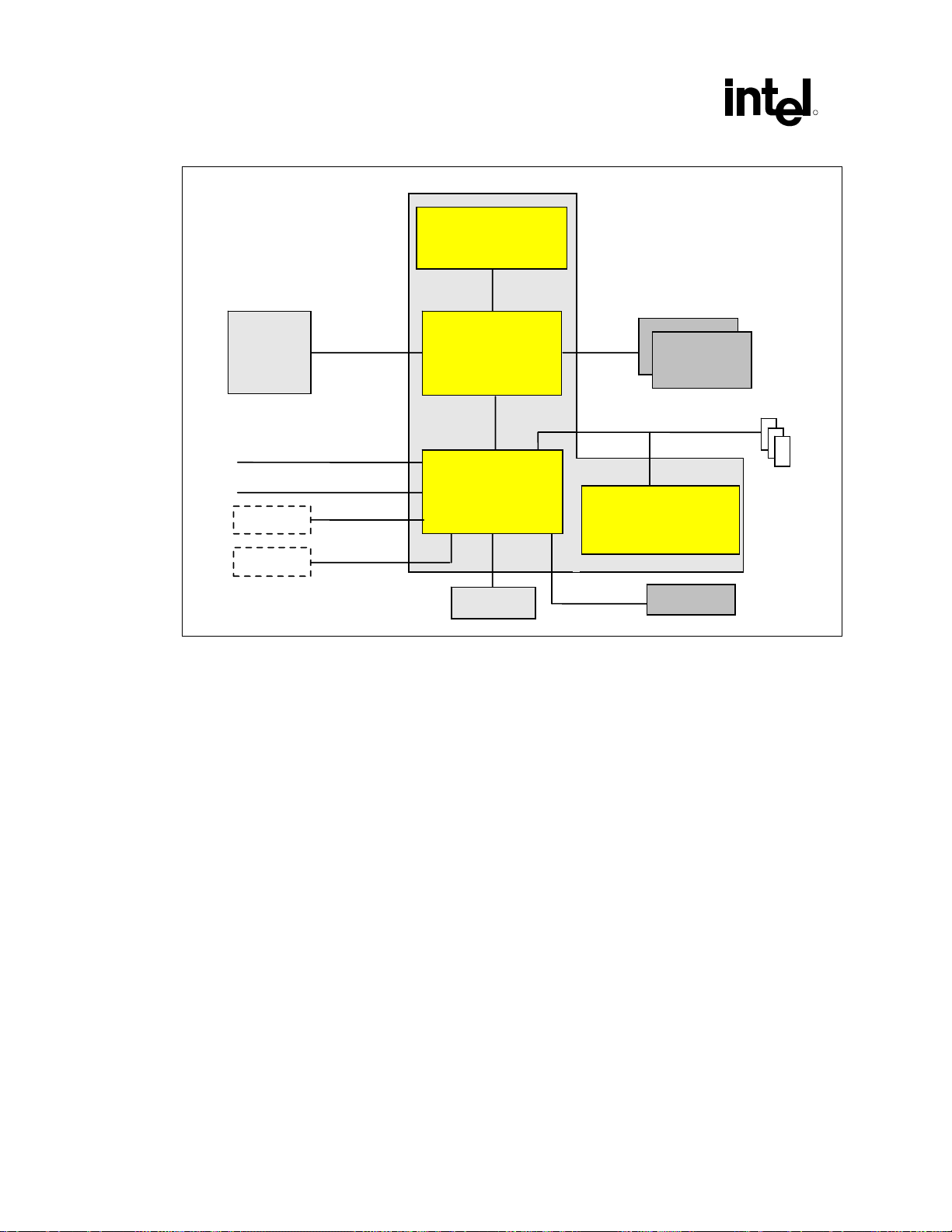
System Overview
Figure 1. Basic System Block Diagram
Intel® Pentium® M or
®
Celeron® M
Intel
Processor
400 MHz FSB
R
AGP
Graphics
Controller
USB2.0/1.1 (6)
IDE (2)
LAN PHY
Codecs
AGP 4X/2X
1.5V
AC97
Intel® 855PM
MCH 593 Micro
FCBGA
Hub
Interface
1.0
Intel® 82801DBM
421 BGA
(ICH4-M)
FWH
200/266/333
MHz DDR
PCI Bus
Mini PCI
Intel® PRO/Wireless
Network Connection
LPC I/F
Super I/O
PCI
Devices
.
24 Intel
®
855PM Chipset Platform Design Guide
Page 25

R
2.2. Intel® Pentium® M Processor/Intel® Celeron® M
Processor
2.2.1. Architectural Features
Supports Intel Architecture with Dynamic Execution
High performance, low-power core
On-die, primary 32-kB instruction cache and 32-kB write-back data cache
On-die, second level cache with Advanced Transfer Cache Architecture
2-MB for Intel Pentium M Processor on 90nm process with 2-MB L2 Cache
1-MB for Intel Pentium M Processor
512-kB for Intel Celeron M Processor
Advanced Branch Prediction and Data Prefetch Logic
System Overview
Streaming SIMD Extensions 2 (SSE2)
400-MHz, Source-Synchronous Front Side Bus
Advanced Power Management features including Enhanced Intel SpeedStep technology (not
supported by Intel Celeron M processor)
2.2.1.1. Packaging/Power
478-pin, Micro-FCPGA and 479-ball Micro-FCBGA packages
V
:
CC-CORE
®
¾ Refer to Intel
Pentium® M Processor Datasheet, Intel® Pentium® M Processor on 90nm
process with 2-MB L2 Cache Datasheet and Intel
CC-CORE
voltages
V
®
Celeron® M Processor Datasheet for
VCCA:
¾ Intel Pentium M processor and Intel Celeron M processor: 1.8 V
¾ Intel Pentium M processor on 90nm process with 2-MB L2 Cache: 1.8 V or 1.5 V
V
(1.05 V)
CCP
2.3. Intel 855PM Memory Controller Hub (MCH)
2.3.1. Front Side Bus Support
Optimized for the Intel Pentium M processor / Intel Celeron M processor in 478-pin Micro-FCPGA
and 479-ball Micro-FCBGA packages
AGTL+ bus driver technology with integrated GTL termination resistors (gated AGTL+ receivers
for reduced power)
®
Intel
855PM Chipset Platform Design Guide 25
Page 26

System Overview
Supports 32-bit AGTL+ bus addressing (no support for 36-bit address extension)
Supports Uni-processor (UP) systems
400 MT/s FSB support (100 MHz)
2X Address, 4X Data
8 deep In-Order Queue
2.3.2. Integrated System Memory DRAM Controller
Supports up to two double-sided SO-DIMMs (four rows populated) with unbuffered
PC1600/PC2100/2700 DDR-SDRAM (with or without ECC)
Supports 64 Mb, 128 Mb, 256 Mb, and 512 Mb technologies for x8 and x16 width devices
Maximum of 2 GB of system memory by using 512-Mb stacked memory technology devices
Supports 200 MHz, 266 MHz and 33MHz DDR devices
64-bit data interface (72-bit with ECC)
PC1600/2100 system memory interface
R
Supports up to 16 simultaneous open pages
Support for SO-DIMM Serial Presence Detect (SPD) scheme via SMBus interface STR power
management support via self refresh mode using CKE
2.3.3. Accelerated Graphics Port (AGP) Interface
Supports AGP 2.0 data transfers
Supports a single AGP (1X/2X/4X) device (either via a connector or on the motherboard)
Only supports 1.5-V VDDQ for AGP electricals
PCI semantic (FRAME# initiated) accesses to DRAM are snooped
AGP semantic (PIPE# and SBA) traffic to DRAM is not snooped on the FSB and is therefore not
coherent with the CPU caches
High priority access support
Delayed transaction support for AGP reads that cannot be serviced immediately
AGP Busy/Stop Protocol support
Support for D3 Hot and Cold Device states
AGP Clamping and Sense Amp control
2.3.4. Packaging/Power
593-pin, Micro-FCBGA package (37.5 mm x 37.5 mm)
V
(1.2 V); VCCSM (2.5 V); 1.5 V; VCCGA, VCCHA, & VCC1_8 (1.8 V); V
CC-MCH
26 Intel
(1.05 V)
CCP
®
855PM Chipset Platform Design Guide
Page 27

R
2.4. Intel 82801DBM I/O Controller Hub (ICH4-M)
The Intel 82801DBM provides the I/O subsystem with access to the rest of the system:
Upstream Accelerated Hub Architecture interface for access to the MCH
PCI 2.2 interface (6 PCI Request/Grant Pairs)
Bus Master IDE controller (supports Ultra ATA 100/66/33)
USB 1.1 and USB 2.0 Host Controllers and support for USB 2.0 High Speed Debug port
I/O APIC
SMBus 2.0 Controller
FWH Interface
LPC Interface
AC’97 2.2 Interface
Alert-On-LAN*
System Overview
IRQ Controller
2.4.1. Packaging/Power
421-pin, BGA package (31 mm x 31 mm)
VCC1_5 (1.5 V main logic voltage); VCCSUS1_5 (1.5 V resume logic voltage); VCCLAN1_5
(1.5 V LAN logic voltage); VCC3_3 (3.3 V main I/O voltage); VCCSUS3_3 (3.3 V resume I/O
voltage); VCCLAN3_3 (3.3 V LAN I/O voltage); V5REF (5 V); V5REF_SUS (5 V); VCCRTC;
VCCHI (1.8 V); V_CPU_IO/V
(1.05 V)
CCP
2.5. Intel PRO/Wireless Network Connection
Ability to connect to 802.11 Wi-Fi Certified networks
Industry standard and extended wireless security support (WEP, 802.1X and Cisco* LEAP)
®
Intel
Intel PROSet software with automatic WLAN switching support enables automatic switching
Intel PROSet software supports Cisco, Check Point, Microsoft and Intel VPN connections†
Intel PROSet software with ad hoc connection wizard support provides a simple interface for
PROSet software with advanced profile management support, allows multiple setup profiles
to connect to different WLAN networks
between wired & wireless LAN connections
setting up ad hoc networks
Intel Wireless Coexistence System support enables reduced interference between Intel
PRO/Wireless & certain Bluetooth* devices
Per-packet antenna selection enables optimized WLAN performance
Intel Intelligent Scanning technology, reduces power by controlling the frequency of scanning for
access points
®
Intel
855PM Chipset Platform Design Guide 27
Page 28

System Overview
Power saving capability with five different power settings allows users to trade off performance
and battery life.
2.5.1. Packaging and Power
Mini-PCI Type 3B: (59.45 mm x 44.45 mm x 5mm)
Mini-PCI Type 3A: (59.45 mm x 50.8 mm x 5 mm)
3.3V
2.6. Firmware Hub (FWH)
An integrated hardware Random Number Generator (RNG)
Register-based locking
Hardware-based locking
Five GPIs
R
2.6.1. Packaging/Power
32-pin TSOP/PLCC
3.3-V core and 3.3 V/12 V for fast programming
28 Intel
®
855PM Chipset Platform Design Guide
Page 29

General Design Considerations
R
3. General Design Considerations
This section documents motherboard layout and routing guidelines for Intel 855PM chipset platforms. It
does not discuss the functional aspects of any bus, or the layout guidelines for an add-in device.
If the guidelines listed in this document are not followed, it is very important that thorough signal
integrity and timing simulations are completed for each design. Even when the guidelines are followed,
Intel recommends that critical signals be simulated to ensure proper signal integrity and flight time. Any
deviation from the guidelines should be simulated.
The trace impedance typically noted (i.e. 55 ± 15%) is the “nominal” trace impedance for a 5-mil
wide external trace and a 4-mil wide internal trace. However, some stack-ups may lead to narrower or
wider traces on internal or external layers in order to meet the 55- impedance target. Note the trace
impedance target assumes that the trace is not subjected to the EMI created by changing current in
neighboring traces. It is important to consider the minimum and maximum impedance of a trace based
on the switching of neighboring traces when calculating flight times. Using wider spaces between the
traces can minimize this trace-to-trace coupling. In addition, these wider spaces reduce settling time.
Coupling between two traces is a function of the coupled length, the distance separating the traces, the
signal edge rate, and the degree of mutual capacitance and inductance. In order to minimize the effects
of trace-to-trace coupling, the routing guidelines documented in this section should be followed. Also,
all high-speed, impedance controlled signals (e.g. FSB signals) should have continuous GND referenced
planes and cannot be routed over or under power/GND plane splits.
3.1. Nominal Board Stack-Up
Systems incorporating the Intel 855PM chipsets requires a board stack-up yielding a target impedance of
55 ± 15%.
An example of an 8-layer board stack-up is shown in Figure 2. The left side of the figure illustrates the
starting dimensions of the metal and dielectric material thickness as well as drawn trace width
dimensions prior to lamination, conductor plating, and etching. After the motherboard materials are
laminated, conductors plated, and etched, somewhat different dimensions result. Dielectric materials
become thinner, under/over etching of conductors alters their trace width, and conductor plating makes
them thicker. It is important to note that for the purpose of extracting electrical models from
transmission line properties, the final dimensions of signals after lamination, plating, and etching should
be used.
The stack-up uses 1.2-mil (1 oz) copper on power planes to reduce I*R drops and 0.6-mil copper
thickness on the signal layers: primary side layer (L1), Layer 3 (L3), Layer 6 (L6), and secondary side
layer (L8). After plating, the external layers become 1.2 to 2 mils thick.
To meet the nominal 55- characteristic impedance primary and secondary side layer micro-strip lines
are drawn at 5-mil trace width but end up with a 5.5-mil final trace width after etching. For the same
reason, the 5-mil thick prepreg between the primary side layer and Layer 2 starts at 5 mils but becomes 4
mils after lamination. This situation and result also applies to Layer 7 and the secondary side layer.
®
Intel
855PM Chipset Platform Design Guide 29
Page 30
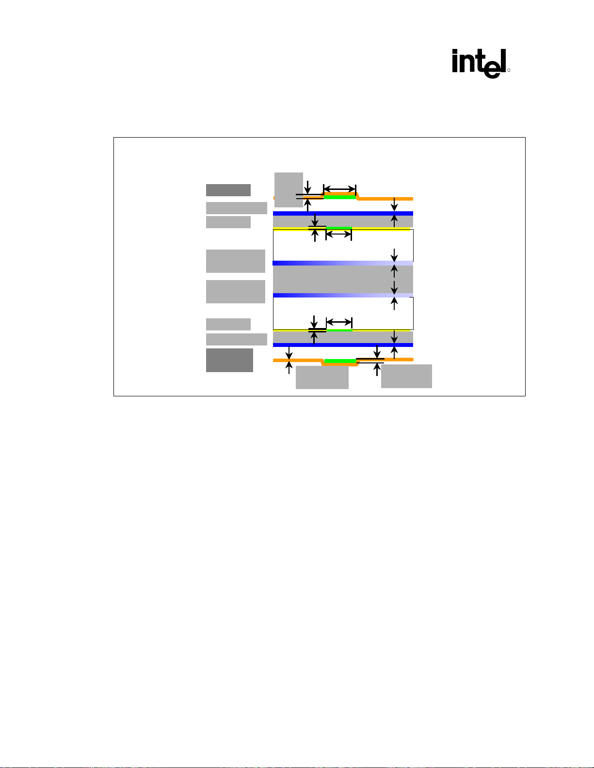
General Design Considerations
To ensure impedance control of 55 , the primary and secondary side layer micro-strip lines should
reference solid ground planes on Layer 2 and Layer 7, respectively.
Figure 2. Recommended Board Stack-Up Dimensions
Er=4.3
Er=4.3
1.5mil
1.5mil
After
L1 Signals
L1 Signals
L2 GND Plane
L2 GND Plane
L2 GND Plane
L3 Signals
L3 Signals
L3 Signals
L4 GND/PWR
L4 GND/PWR
L4 GND/PWR
Plane
Plane
Plane
L5 GND/PWR
L5 GND/PWR
L5 GND/PWR
Plane
Plane
Plane
L6 Signals
L6 Signals
L6 Signals
L7 GND Plane
L7 GND Plane
L7 GND Plane
L8 Signals/
L8 Signals/
Power
Power
After
plating
plating
Final Dimensions after
Final Dimensions after
Lamination, Etching, Plating
Lamination, Etching, Plating
5.0mil
5.0mil
Prepreg 4.0mil
Prepreg 4.0mil
Core 4.0mil
Core 4.0mil
4.0mil
0.6mil
0.6mil
Prepreg 11.0mil
Prepreg 11.0mil
Prepreg 11.0mil
Prepreg 11.0mil
0.6mil
0.6mil
1.0mil
1.0mil
Solder Mask
Solder Mask
Core 12.0mil
Core 12.0mil
Core 4mil
Core 4mil
Prepreg 4.0mil
Prepreg 4.0mil
4.0mil
4.0mil
4.0mil
1.2mil
1.2mil
1.2mil
1.2mil
1.2mil
1.2mil
1.2mil
1.2mil
1.5mil
1.5mil
After plating
After plating
R
Internal signal traces on Layer 3 and Layer 6 are unbalanced strip-lines. To meet the nominal 55-
characteristic impedance for these traces, they reference a solid ground plane on Layer 2 and Layer 7.
Since the coupling to Layer 4 and Layer 5 is still significant, (especially true when thinner stack-ups use
balanced strip-lines on internal layers) these layers are converted to ground floods in the areas of the
motherboard where the high-speed interfaces like the FSB or DDR system memory are routed. In the
remaining sections of the motherboard layout the Layer 4 and Layer 5 layers are used for power
delivery.
For 55- characteristic impedance Layer 3 (Layer 6), strip-lines have a 4-mil final trace width and are
separated by a core dielectric thickness of 4 mils after lamination from the Layer 2 (Layer 7) ground
plane and 11-mil thickness prepreg after lamination to separate it from Layer 4 (Layer 5). The starting
thickness of these core and prepreg dielectric layers before lamination is 5 mils and 12 mils,
respectively.
The secondary side layer is also used for power delivery in many cases since it benefits from the thick
copper plating of the external layer plating as well as referencing the close (4-mil prepreg thickness)
Layer 7 ground plane. The benefit of such a stack-up is low inductance power delivery.
OEMs may choose to use different stack-ups (number of layers, thickness, trace width, etc.) from the
one example outlined in Figure 2. However, the following key elements should be observed:
1. Final post lamination, post etching, and post plating dimensions should be used for electrical
model extractions.
2. Power plane layers should be 1 oz thick and signal layers should be ½ oz thick.
3. External layers become 1 – 1.5 oz (1.2 – 2 mils) thick after plating
30 Intel
®
855PM Chipset Platform Design Guide
Page 31

General Design Considerations
R
4. All high-speed signals should reference solid ground planes through the length of their routing
and should not cross plane splits. To guarantee this, both planes surrounding strip-lines should be
GND.
5. Intel recommends that high-speed signal routing be done on internal, strip-line layers.
6. High-speed signals transitioning between layers next to the component, signal pins should be
accounted for by the GND stitching vias that would stitch all the GND plane layers in that area of
the motherboard. Due to the arrangement of the Intel® Pentium® M Processor / Intel® Celeron®
M Processor and Intel 855PM MCH pin-maps, GND vias placed near all GND lands will also be
very close to high-speed signals that may be transitioning to an internal layer. Thus, no additional
ground stitching vias (besides the GND pin vias) are required in the immediate vicinity of the
processor and MCH packages to accompany the signal transitions from the component side into
an internal layer.
7. High-speed routing on external layers should be minimized in order to avoid EMI. Routing on
external layers also introduces different delays compared to internal layers, making it extremely
difficult to do length matching if some routing is done on both internal and external layers.
®
Intel
855PM Chipset Platform Design Guide 31
Page 32

General Design Considerations
R
This page intentionally left blank.
32 Intel
®
855PM Chipset Platform Design Guide
Page 33

R
4. FSB Design Guidelines
The following layout guidelines support designs using the Intel Pentium M processor / Intel Celeron M
processor and the Intel 855PM MCH chipset. Due to on-die Rtt resistors on both the processor and the
chipset, additional resistors do not need to be placed on the motherboard for most FSB signals. A simple
point-to-point interconnect topology is used in these cases.
4.1. FSB Design Recommendations
For proper operation of the processor and the chipset, the system designer must meet the timing and
voltage specification of each component. The following recommendations are Intel’s best guidelines
based on extensive simulation and experimentation that make assumptions, which may be different than
an OEM’s system design. The most accurate way to understand the signal integrity and timing of the
FSB in your platform is by performing a comprehensive simulation analysis. It is possible that
adjustments to trace impedance, line length, termination impedance, board stack-up, and other
parameters can be made that improve system performance.
FSB Design Guidelines
®
Refer to the latest Intel
process with 2-MB L2 Cache Datasheet or Intel
signal types, and definitions. Below are the design recommendations for the data, address, and strobes.
For the following discussion, the pad is defined as the attach point of the silicon die to the package
substrate. The guidelines are derived from empirical testing with Intel 855PM chipset MCH package
models.
Pentium® M Processor Datasheet, Intel® Pentium® M Processor on 90nm
®
Celeron® M Processor Datasheet for a FSB signal list,
4.1.1. Recommended Stack-up Routing and Spacing Assumptions
The following section describes in more detail, the terminology and definitions used for different routing
and stack-up assumptions that apply to the recommended motherboard stack-up show in Figure 2.
4.1.1.1. Trace Space to Trace – Reference Plane Separation Ratio
Figure 3 illustrates the recommended relationship between the edge-to-edge trace spacing (2X) versus
the trace to reference plane separation (X). An edge-to-edge trace spacing (2X) to trace – reference
plane separation (X) ratio of 2 to 1 ensures a low crosstalk coefficient. All the effects of crosstalk are
difficult to simulate. The timing and layout guidelines for the Intel Pentium M/Intel Celeron M
processor have been created with the assumption of a 2:1 trace spacing to trace – reference plane ratio.
A smaller ratio would have an unpredictable impact due to crosstalk.
®
Intel
855PM Chipset Platform Design Guide 33
Page 34

FSB Design Guidelines
Figure 3. Trace Spacing vs. Trace to Reference Plane Example
Reference Plane (VSS)
Trace
4.1.1.2. Trace Space to Trace Width Ratio
Figure 4 illustrates the recommended relationship between the edge-to-edge trace spacing versus trace
width ratio for the best signal quality results. In general, a 3:1 trace space to trace width ratio is preferred
and highly recommended. In case of routing difficulties on the motherboard, using a 2:1 ratio would be
acceptable only if additional simulations conclude that it is possible, and this may include some changes
to the stack-up or routing assumptions. In the case of the FSB signals, routing recommendations for a
2:1 trace spacing to trace width ratio can be found in Topology 2 for the source synchronous signals (see
Table 5).
R
X
2X
Trace
Figure 4. Trace Spacing vs. Trace Width Example
v
3X
Trace
Trace
v
X
4.1.1.3. Recommended Stack-up Calculated Coupling Model
The importance of maintaining an adequate trace space to trace width ratio is to achieve the best signal
quality possible given routing constraints. The simulations performed that resulted in the recommended
3:1 trace space to trace width ratio is to keep the coupling between adjacent traces below a maximum
value. For the recommended stack-up, the constants shown in Figure 5 are assumed to be constant for a
typical stack-up. This means the mutual to self-coupling relationship given below does not take into
account the normal tolerances that are allowed for in the recommended board stack-up’s parameters. For
the recommended stack-up shown in Figure 2, the calculated capacitive coupling maximum value is
represented by the following relationship:
/ C
( C
MUTUAL
) x 100 = 8.15%
SELF
As shown in Figure 5, the coupling values are calculated based on a three-line model, represented by
Trace 1, Trace 2, and Trace 3. Based on the capacitive coupling model shown, the aforementioned
parameters are:
= C21 + C23
C
MUTUAL
34 Intel
®
855PM Chipset Platform Design Guide
Page 35

R
C
= C22 (Trace 2, i.e. CS2a + CS2b)
SELF
If a stack-up that is employed does not adhere to the recommended stack-up, then a new extraction must
be made for the stack-up using a 2D field solver program. According to the 2D field solver results, new
coupling calculations must be performed to ensure that the coupling results are less than the
aforementioned capacitive coupling maximum value of 8.15%. If the coupling results are greater than
the maximum value, then additional system level simulations must be performed to avoid any signal
quality issues due to crosstalk effects.
Figure 5. Recommended Stack-up Capacitive Coupling Model
Note : CS1a + CS1b = C11
CS2a + CS2b = C22
CS3a +CS3b = C33
GND
FSB Design Guidelines
CS2aCS1a
CS3a
11.2 Mil
Trace 1 Trace 2 Trace 3
C21 C23
CS1b
CS2b
CS3b
4.8 Mil
GND
4.1.1.4. Signal Propagation Time to Distance Relationship and Assumptions
Due to the high frequency nature of some interfaces and signals, length matching may or may not exist
as part of the routing requirements for a given interface. In general, the tolerances that specific signals in
a bus must be routed to will be stated as a length measured in mils or inches and is specific to the
recommended motherboard stack-up (see Figure 2). However, some length matching tolerances for
signals listed in this design guide may be stated as a measurement of time. In such cases, the correlation
of the period of time to an actual length value will depend on board stack-up.
Based on the recommended stack-up, the signal propagation time to distance relationship, for the
purpose of this design guide, is as follows:
Strip-line (internal layer) Routing: 180 ps for 1.0 inch
Micro-strip (external layer) Routing: 162 ps for 1.0 inch
For example, a length-matching requirement of ± 50 ps for routing on a strip-line (internal) layer would
correlate to a trace length whose tolerance is within ± 278 mils of an associated trace. The signal
propagation time to distance relationship listed above is based on a single transmission line model
incorporating a typical stack-up. Thus, no other signals or traces are accounted for in such a model and
there is an assumption of zero coupling with other traces. Also, the recommended stack-up’s parameter
tolerances are not taken into account in the “typical” stack-up assumptions. Finally, in cases that need to
account for worst-case stack-up parameters and for even or odd mode coupling, new extractions from
the stack-up model must be done to provide an accurate signal propagation time to distance relationship.
®
Intel
855PM Chipset Platform Design Guide 35
Page 36

FSB Design Guidelines
4.1.2. Common Clock Signals
All common clock signals use an AGTL+ bus driver technology with on die integrated GTL termination
resistors connected in a point-to-point, Zo = 55 , controlled impedance topology between the processor
and the Intel 855PM chipset MCH. No external termination is needed on these signals. These signals
operate at the FSB frequency of 100 MHz.
Common clock signals should be routed on an internal or external layer while referencing solid ground
planes. Common clock signal routing on internal layers implemented with complete reference to ground
planes both above and below the signal layer is recommended. Based on current simulation results,
routing on internal layers allows for a minimum pin-to-pin motherboard length of 1.0 inch and a
maximum of 6.5 inches. Routing on external layers allows for a pin-to-pin motherboard length of 1.0
inch and a maximum of 6.5 inches. Trace length matching for the common clock signals is not required.
Intel recommends routing these signals on the same internal or external layer for the entire length of the
bus. If routing constraints require routing of these signals with a transition to a different layer, a
minimum of one ground stitching via for every two signals should be placed within 100 mils of the
signal transition vias.
Routing of the common clock signals should use a minimum of 1:2 trace spacing. This implies a 4-mil
trace width with a minimum of 8-mil spacing (i.e. 12-mil minimum pitch) for routing on internal layers.
For external layers, route using a 5-mil trace width and a 10-mil minimum spacing (i.e. 15-mil pitch).
Practical cases of escape routing under the MCH or the processor package outline and near by vicinity
may not allow the implementation of 1:2 trace spacing requirements. Although every attempt should be
made to maximize the signal spacing in these areas, it is allowable to have 1:1 trace spacing underneath
the MCH and the processor package outlines and up to 200 – 300 mils outside the package outline.
R
Table 1 summarizes the list of common clock and key routing requirements. RESET# (CPURST# of
MCH) is also a common clock signal but requires a special treatment for the case where an
ITP700FLEX debug port is used. See Section 4.1.5 for further details. Figure 6 and Figure 7 illustrate
an example of escape routing from the processor and the Intel 855PM chipset MCH package vicinity for
the common clock signals. To allow for flat routing, DEFER#, DRDY#, HIT#, HITM#, TRDY#, and
BNR# would have to have minimal routing on the primary side in the vicinity of the MCH package and
then the rest of the routing continues on internal layer 6. The ground vias of the MCH pins provide the
needed ground stitching vias for a layer transition for these signals. The remaining signals have standard
dog bone (a land for a BGA ball followed by a short trace to a via with a 25-mil offset in the X and Y
directions) vias on the primary side and continue to the processor in a simple point-to-point connection.
The processor only has straightforward dog bones on the primary side for this group of signals. Figure 8
shows a global routing summary of these common clock signals as a simple point-to-point connection
on Layer 6 between the processor and the Intel 855PM MCH.
36 Intel
®
855PM Chipset Platform Design Guide
Page 37

R
Table 1. FSB Common Clock Signal Internal Layer Routing Guidelines
FSB Design Guidelines
Signal Names Total Trace Length
CPU MCH
ADS# ADS# Strip-line 1.0 6.5 55 ± 15% 4 & 8
BNR# BNR# Strip-line 1.0 6.5 55 ± 15% 4 & 8
BPRI# BPRI# Strip-line 1.0 6.5 55 ± 15% 4 & 8
BR0# BREQ0# Strip-line 1.0 6.5 55 ± 15% 4 & 8
DBSY# DBSY# Strip-line 1.0 6.5 55 ± 15% 4 & 8
DEFER# DEFER# Strip-line 1.0 6.5 55 ± 15% 4 & 8
DPWR# DPWR# Strip-line 1.0 6.5 55 ± 15% 4 & 8
DRDY# DRDY# Strip-line 1.0 6.5 55 ± 15% 4 & 8
HIT# HIT# Strip-line 1.0 6.5 55 ± 15% 4 & 8
HITM# HITM# Strip-line 1.0 6.5 55 ± 15% 4 & 8
LOCK# HLOCK# Strip-line 1.0 6.5 55 ± 15% 4 & 8
RS[2:0]# RS[2:0]# Strip-line 1.0 6.5 55 ± 15% 4 & 8
TRDY# HTRDY# Strip-line 1.0 6.5 55 ± 15% 4 & 8
RESET#1 CPURST# Strip-line 1.0 6.5 55 ± 15% 4 & 8
Transmission Line
Type
Min
(inches)
Max
(inches)
Nominal
Impedance
( )
Width &
spacing
(mils)
NOTE: For topologies where an ITP700FLEX debug port is implemented, see Section 4.1.5 for RESET#
(CPURST#) implementation details.
®
Intel
855PM Chipset Platform Design Guide 37
Page 38

FSB Design Guidelines
Table 2. FSB Common Clock Signal External Layer Routing Guidelines
R
Signal Names Total Trace Length
CPU MCH
ADS# ADS# Micro-strip 1.0 6.5 55 ±15% 5 & 10
BNR# BNR# Micro-strip 1.0 6.5 55 ±15% 5 & 10
BPRI# BPRI# Micro-strip 1.0 6.5 55 ± 15% 5 & 10
BR0# BREQ0# Micro-strip 1.0 6.5 55 ± 15% 5 & 10
DBSY# DBSY# Micro-strip 1.0 6.5 55 ± 15% 5 & 10
DEFER# DEFER# Micro-strip 1.0 6.5 55 ± 15% 5 & 10
DPWR# DPWR# Micro-strip 1.0 6.5 55 ± 15% 5 & 10
DRDY# DRDY# Micro-strip 1.0 6.5 55 ±15% 5 & 10
HIT# HIT# Micro-strip 1.0 6.5 55 ±15% 5 & 10
HITM# HITM# Micro-strip 1.0 6.5 55 ±15% 5 & 10
LOCK# HLOCK# Micro-strip 1.0 6.5 55 ± 15% 5 & 10
RS[2:0]# RS[2:0]# Micro-strip 1.0 6.5 55 ± 15% 5 & 10
TRDY# HTRDY# Micro-strip 1.0 6.5 55 ± 15% 5 & 10
RESET#1 CPURST# Micro-strip 1.0 6.5 55 ± 15% 5 & 10
Transmission Line
Type
Min
(inches)
Max
(inches)
Nominal
Impedance
( )
Width &
spacing
(mils)
NOTE: For topologies where an ITP700FLEX debug port is implemented, see Section 4.1.5 for RESET#
(CPURST#) implementation details.
38 Intel
®
855PM Chipset Platform Design Guide
Page 39

R
Figure 6. Common Clock Signals Example – Intel 855PM MCH Escape Routing
FSB Design Guidelines
Layer 6
DPSLP#
RESET#
PRIMARY SIDE
COMMON
Clock
Signals
Figure 7. Common Clock Signals Example – Processor Escape Routing
Layer 6
HIT#
DEFER#
DRDY#
HITM#
TRDY#
BNR#
DPSLP#
RESET#
COMMON
Clock
Signals
®
Intel
855PM Chipset Platform Design Guide 39
Page 40

FSB Design Guidelines
Figure 8. Common Clock Signals Example – Processor to Intel 855PM MCH Layer 6 Routing
Mother Board Layer 6 routing
Mother Board Layer 6 routing
Mother Board Layer 6 routing
Mother Board Layer 6 routing
Mother Board Layer 6 routing
Mother Board Layer 6 routing
Mother Board Layer 6 routing
Mother Board Layer 6 routing
Mother Board Layer 6 routing
Mother Board Layer 6 routing
Mother Board Layer 6 routing
Mother Board Layer 6 routing
Intel®
Intel®
Intel®
Intel®
Intel®
Intel®
Intel®
Intel®
Intel Pentium M
Intel Pentium M
Intel Pentium M
Intel Pentium M
Pentium M
Pentium M
Pentium M
Pentium M
Pentium M
Pentium M
Pentium M
Pentium M
Pentium M
Pentium M
Pentium M
Pentium M
processor
processor
processor
processor
Pentium® M
Pentium® M
Pentium® M
Pentium® M
Pentium® M
Pentium® M
Pentium® M
Pentium® M
Intel
Intel
Intel
Intel
Intel®
Intel®
Intel®
Intel®
Intel®
Intel®
Intel®
Intel®
Intel®
Intel®
Intel®
Intel®
855PM
855PM
855PM
855PM
855PM
855PM
855PM
855PM
855PM
855PM
855PM
855PM
855PM
855PM
855PM
855PM
855PM
855PM
855PM
855PM
855PM
855PM
855PM
855PM
855PM
855PM
855PM
855PM
MCH-M
MCH-M
MCH-M
MCH-M
MCH
MCH
MCH-M
MCH-M
MCH-M
MCH-M
MCH-M
MCH-M
MCH-M
MCH-M
MCH-M
MCH-M
MCH-M
MCH-M
COMMON
COMMON
COMMON
COMMON
COMMON
COMMON
COMMON
COMMON
COMMON
COMMON
COMMON
COMMON
Clock Signals
Clock Signals
Clock Signals
Clock Signals
Clock Signals
Clock Signals
Clock Signals
Clock Signals
Clock Signals
Clock Signals
Clock Signals
Clock Signals
R
40 Intel
®
855PM Chipset Platform Design Guide
Page 41

R
4.1.3. Source Synchronous Signals
All source synchronous signals use an AGTL+ bus driver technology with on-die GTL termination
resistors connected in a point-to-point, Zo = 55 controlled impedance topology between the Intel
Pentium M/Intel Celeron M processor and the Intel 855PM MCH. No external termination is needed on
these signals. Source synchronous FSB address signals operate at a double pumped rate of 200 MHz
while the source synchronous FSB data signals operate at a quad pumped rate of 400 MHz. High-speed
operation of the source synchronous signals requires careful attention to their routing considerations.
The following guidelines should be strictly adhered to, to guarantee robust high-frequency operation of
these signals.
4.1.3.1. Source Synchronous General Routing Guidelines
Source synchronous data and address signals and their associated strobes are partitioned into groups of
signals. Flight time skew minimization within the same group of source synchronous signals is a key
parameter that allows their high frequency (400 MHz) operation. All the source synchronous signals that
belong to the same group should be routed on the same internal layer for the entire length of the bus.
It is acceptable to split different groups of source synchronous signals between different motherboard
layers as long as all the signals that belong to that group are kept on the same layer. Grouping of FSB
source synchronous signals is summarized in Table 3 and Table 6. This practice results in a significant
reduction of the flight time skew since the dielectric thickness, line width, and velocity of the signals
will be uniform across a single layer of the stack-up. There is no guarantee of a relationship of dielectric
thickness, line width, and velocity between layers.
FSB Design Guidelines
The source synchronous signals should be routed as a strip-line on an internal layer with complete
reference to ground planes both above and below the signal layer. Routing with references to split
planes or power planes other than ground is not allowed. For the recommended stack-up example as
shown in Figure 2, source synchronous FSB signals are routed on Layer 3 and Layer 6. Layer 2 and
Layer 7 are solid grounds across the entire motherboard. However, this is not sufficient since significant
coupling exists between signal Layer 3 and power plane Layer 2 as well as signal Layer 6 and power
plane Layer 5. To guarantee complete ground referencing, Layer 4 and Layer 5 are converted to ground
plane floods in the areas where the source synchronous FSB signals are routed. In addition all the
ground plane areas are stitched with ground vias in the vicinity of the processor and Intel 855PM MCH
package outlines with the vias of the ground pins of the processor and MCH pin-map.
Figure 9 illustrates a motherboard layout and a cross-sectional view of the recommended stack-up of the
FSB source synchronous DATA and ADDRESS signals referencing ground planes on both Layer 7 and
Layer 5. Notice that in the socket cavity of the processor Layer 5 and Layer 6 layers is used for VCC
core power delivery. However, outside the socket cavity Layer 6 signals are routed on top of a solid
Layer 7 ground plane and also Layer 5 is converted to a ground flood under the shadow of the FSB
signals routing between the processor and MCH. Stitching of all the GND planes is provided by the
ground vias in the pin-map of the processor and MCH.
®
Intel
855PM Chipset Platform Design Guide 41
Page 42

FSB Design Guidelines
Figure 9. Layer 6 FSB Source Synchronous Signals GND Referencing to Layer 5 and Lay er 7
Ground Planes
R
L6 and L5 top side view
VCC
Stackup cross-section
L4
L5
GND
L6
L7
BSB DATA
GND
VCC
BSB ADDRESS
In a similar way, Figure 10 illustrates a recommended layout and stack-up example of how another
group of FSB source synchronous DATA and ADDRESS signals can reference ground planes on both
Layer 2 and Layer 4. Note that in the socket cavity of the processor, Layer 3 is used for VCC core
power delivery to reduce the I*R drop. However, outside of the socket cavity Layer 3 signals are routed
below a solid Layer 2 ground plane and also Layer 4 is converted to a ground flood under the shadow of
the FSB signals routing between the processor and MCH.
Figure 10. Layer 3 FSB Source Synchronous Signals GND Referencing to Layer 2 and Lay er 4
Ground Planes
L3 and L4 top side view
VCC
Stackup cross-section
L2
L3
L4
BSB DATA
BSB ADDRESS
100MHz CLKs
GND
GND
VCC
42 Intel
®
855PM Chipset Platform Design Guide
Page 43

R
Skew minimization requires pin-to-pin trace length matching of the FSB source synchronous signals that
belong to the same group including the strobe signals of that group. Trace length matching of the
processor and MCH packages does not need to be accounted for in the motherboard routing since both
packages have the source synchronous signals and the strobes length matched within the group inside
the package routing.
Current simulation results provide routing guidelines using 1:3 spacing (Topology 1) for the FSB source
synchronous signals. This implies 4-mil trace width with a minimum of 12-mil spacing (i.e. 16-mil
minimum pitch). Practical cases of escape routing under the MCH or processor package outline and near
by vicinity may not even allow the implementation of 1:2 trace spacing requirements. Although every
attempt should be made to maximize the signal spacing in these areas, it is allowable to have 1:1 trace
spacing underneath the MCH and the processor package outlines and up to 200 – 300 mils outside the
package outline.
Routing guidelines using 1:2 spacing is available and can be used wherever 1:3 spacing cannot be
implemented by using Topology 2. The benefits of additional spacing include increased signal quality
and voltage margining. The trace routing and length matching requirements are provided in the
following sections.
4.1.3.2. Source Synchronous – Data
FSB Design Guidelines
Robust operation of the 400-MHz, source synchronous data signals require tight skew control. For this
reason, these signals are split into matched groups as outlined in Table 3. All the signals within the same
group should be kept on the same layer of motherboard routing and should be routed to the same pad-topad length within ± 100 mils of the associated strobes. Because the processor and Intel 855PM MCH
packages provide package trace equalization for signals within each data group, all signals should be
routed on the system board to meet the pin-to-pin matching requirement of ± 100 mils. The two
complementary strobe signals associated with each group should be length matched to each other within
± 25 mils and tuned to the average length of the data signals of their associated group. This will
optimize setup/hold time margin.
Table 3. FSB Data Source Synchronous Signal Trace Length Mismatch Mapping
CPU Signal Name Signal Matching
D[15:0]#, DINV0# ± 100 mils DSTBP0#, DSTBN0# ± 25 mils 1
D[31:16]#, DINV1# ± 100 mils DSTBP1#, DSTBN1# ± 25 mils 1
D[47:32]#, DINV2# ± 100 mils DSTBP2#, DSTBN2# ± 25 mils 1
D[63:48]#, DINV3# ± 100 mils DSTBP3#, DSTBN3# ± 25 mils 1
NOTE: Strobes of the same group should be trace length matched to each other within ±25 mil and to the average
length of their associated Data signal group.
Strobes associated With the
Group
Strobe Matching Notes
Table 4 lists the source synchronous data signal general routing requirements. Due to the 400-MHz,
high-frequency operation of the data signals, 1:3 spacing is strongly advised and should be limited to a
pin-to-pin trace length minimum of 0.5 inches and maximum of 5.5 inches.
®
Intel
855PM Chipset Platform Design Guide 43
Page 44

FSB Design Guidelines
Table 4. FSB Source Synchronous Data Signal Routing Guidelines Topology 1
R
Signal Names Total Trace Length
CPU MCH
DINV[3:0]# DBI[3:0]# Strip-line 0.5 5.5 55 ± 15% 4 & 12
D[63:0]# HD[63:0]# Strip-line 0.5 5.5 55 ±15% 4 & 12
DSTBN[3:0]# HDSTBN[3:0]# Strip-line 0.5 5.5 55 ± 15% 4 & 12
DSTBP[3:0]# HDSTBP[3:0]# Strip-line 0.5 5.5 55 ±15% 4 & 12
Transmission
Line Type
Min
(inches)
Max
(inches)
Nominal
Impedance
( )
If routing space constraints do not allow 1:3 spacing of the source synchronous data signals, Table 5
lists alternative routing requirements for some of these signals if 1:2 spacing is used. In both topologies,
the pin-to-pin trace length should be limited to a minimum of 0.5 inches and a maximum of 5.5 inches.
The adherence to tighter characteristic trace impedance tolerances for the alternative routing
requirements allows the closer spacing of the data and bus inversion signals to be achieved. The use of ±
10% tolerance for the trace impedance in the alternative topology allows designs to maintain the same
overall minimum and maximum trace lengths as the primary topology that utilizes a looser ± 15%
tolerance. Although the data and bus inversion signals for the FSB can be routed with 1:2 spacing when
using the tighter trace impedance tolerance, the data strobes must maintain 1:3 spacing. In this case, the
processor’s DSTBN[3:0]# and DSTBP[3:0]# strobe signals must be routed to the MCH’s
HDSTBN[3:0]# and HDSTBP[3:0]# strobe signals with 1:3 spacing from all signals even if ± 10% trace
impedance tolerance is used.
Table 5. FSB Source Synchronous Data Signal Routing Guidelines Topology 2
Width &
spacing (mils)
Signal Names Total Trace Length
CPU MCH
DINV[3:0]# DBI[3:0]# Strip-line 0.5 5.5 55 ± 10% 4 & 8
D[63:0]# HD[63:0]# Strip-line 0.5 5.5 55 ± 10% 4 & 8
DSTBN[3:0]# HDSTBN[3:0]# Strip-line 0.5 5.5 55 ±10% 4 & 12
DSTBP[3:0]# HDSTBP[3:0]# Strip-line 0.5 5.5 55 ± 10% 4 & 12
Transmission
Line Type
4.1.3.3. Source Synchronous – Address
Source synchronous address signals operate at 200 MHz. Thus, their routing requirements are very
similar to the data signals. Refer to Sections 4.1.3.1 and 4.1.3.2 for further details. Table 6 details the
partition of the address signals into matched length groups. Due to the lower operating frequency of the
address signals, pin-to-pin length matching is relaxed to ± 200 mils. Each group is associated with only
one strobe signal. To maximize setup/hold time margin, the address strobes should be trace length
matched to the average trace length of the address signals of their associated group. In addition, each
address signal should be trace length matched within ± 200 mils of its associated strobe signal.
Min
(inches)
Max
(inches)
Nominal
Impedance
( )
Width & spacing
(mils)
44 Intel
®
855PM Chipset Platform Design Guide
Page 45

R
Table 6. FSB Address Source Synchronous Signal Trace Length Mismatch Mapping
FSB Design Guidelines
CPU Signal Name Signal Matching Strobe Associated With the Group
REQ[4:0]#, A[16:3]# ± 200 mils ADSTB0# ± 200 mils 1, 2
A[31:17]# ± 200 mils ADSTB1# ± 200 mils 1, 2
NOTES:
1. ADSTB[1:0]# should be trace length matched to the average length of their associated Address signals group.
2. Each Address signal should be trace length matched to its associated Address Strobe within ± 200 mils.
Table 7 lists the source synchronous address signals general routing requirements. Due to the 200-MHz,
high frequency operation of the address signals, 1:3 spacing is strongly advised and trace lengths should
be limited to a pin-to-pin trace length minimum of 0.5 inches and a maximum of 6.5 inches. The routing
guidelines listed in Table 7 allows for 1:2 spacing for the address signals given a 55 ± 15%
characteristic trace impedance. But if space permits, 1:3 spacing should be applied to these signals. For
the address strobes, 1:3 spacing is required irrespective of the tolerance of the trace impedance. This is a
change from previous recommendations where 1:2 spacing was acceptable for ± 15% impedance
tolerances.
Table 7. FSB Source Synchronous Address Signal Routing Guidelines
Signal Names Total Trace Length
CPU MCH
A[31:3]# HA[31:3]# Strip-line 0.5 6.5 55 ± 15% 4 & 8
Transmission
Line Type
Min
(inches)
Max
(inches)
Strobe to Assoc. Address
Signal Matching
Nominal
Impedance
( )
Width & Spacing
(mils)
Notes
REQ[4:0]# HREQ[4:0]# Strip-line 0.5 6.5 55 ± 15% 4 & 8
ADSTB#[1:0] HADSTB[1:0]# Strip-line 0.5 6.5 55 ± 15% 4 & 12
4.1.3.4. Source Synchronous Signals Recommended Layout Example
Figure 11 illustrates escape routing of the FSB source synchronous signals in the vicinity of the Intel
855PM MCH package. The primary side has minimum length dog bones from the BGA lands that
transition with vias into internal routing Layer 3 and Layer 6. Note the change in orientation of the dog
bone “dipoles” as it changes from place to place to allow smooth escape routing on Layer 3 and Layer 6
later on in between the GND vias. The signals are split about half and half between Layer 3 and Layer 6.
For address signals, the first group containing REQ[4:0]#, A[16:3]#, and ADSTB[0]# are routed on
Layer 3. The second group of address signals containing A[31:17]# and ADSTB[1]# is routed on Layer
6. Similarly, D[15:0]#, DINV[0]#, DSTBN[0]#, DSTBP[0]# and D[47:32]#, DINV[2]#, DSTBN[2]#,
DSTBP[2]# are routed on Layer 3. The remaining two data signals groups with associated strobe and
DINV signals are routed on Layer 6. A vertical corridor with no routing on Layer 6 to the left of the
D[63:48]# group is used to feed the 1.2-V core power plane of the MCH.
Figure 11 also illustrates how a horizontal corridor with no routing on Layer 3 in between the address
and data signals allows feeding of the VCCA (1.8 V) power plane to the PLL power delivery pins
VCCGA and VCCHA of the Intel 855PM MCH and continues to the VCCA[3:0] pins of the processor.
Notice that this 1.8-V VCCA power plane “forks” as a separate branch from the 1.8-V decoupling
capacitor while the Hub Interface (HI) 1.8-V power pins connect to a separate branch of the 1.8-V
power plane flood on Layer 3. This is done to reduce noise pickup of the PLL power delivery due to HI
switching activity.
®
Intel
855PM Chipset Platform Design Guide 45
Page 46

FSB Design Guidelines
Figure 12 illustrates the processor socket vicinity escape routing of the source synchronous FSB signals
and their successful coexistence with robust power delivery. All source synchronous signals are
connected with minimum length dog bones from the BGA lands of the socket on the primary side layer
into internal layers Layer 3 and Layer 6. In Figure 11, note the changing orientation of the dog bone
“dipoles” as they rotate around the sides of the pin field to guarantee smooth escape routing on Layer 3
and Layer 6.
In addition to signal routing on the primary side, Layer 3 and Layer 6 are also used to feed the core
power delivery into the areas free of signals routing. VCCA (1.8 V) starts from the MCH in Figure 11
and is routed on Layer 3 and is connected with a cluster of vias to a VCCA flood on the primary side
layer. This feeds the primary side “U shape” on the three sides of the processor socket that feeds the
VCCA[3:0] pins. To minimize loop inductance of the VCCA (1.8 V) vias, they are accompanied by two
GND stitching vias.
Figure 13 shows a global view of FSB source synchronous signal routing and its coexistence with a
robust power delivery layout solution. Source synchronous signals are serpentine length matched on
Layer 3 and Layer 6 in the area in between the processor and Intel 855PM MCH packages per the
procedure described in Section 4.1.3.5. Also, the source synchronous address signals route around the
thermal backing plate hole and utilize the space on Layer 3 and Layer 6 in the socket vicinity to perform
trace length equalization.
R
Since GTLREF generation and the COMP[3:0] resistor connections minimize via use, there is minimal
interaction between these vias with the routing of the source synchronous signals. Refer to Section 4.1.7,
Figure 29, Figure 31, and Section 4.1.8.1 for further details.
Also the complete corridor flood routing of VCCA from the MCH can be seen on Figure 13 starting on
Layer 3 and then transitioning to the primary side of the motherboard with the cluster of vias next to the
processor socket. Figure 13 also illustrates why the 100-MHz clocks that are routed on Layer 3 can not
get to the processor pins on either Layer 3 nor Layer 6. Thus, the two clocks transition to the secondary
side of the motherboard (not shown in Figure 13) to obtain the shortest vertical distance to the
processor’s BCLK[1:0] pins and the ITP_CLK[1:0] pins of the ITP700FLEX debug port. See Section
4.3.1 for further details.
46 Intel
®
855PM Chipset Platform Design Guide
Page 47

FSB Design Guidelines
R
Figure 11. Intel 855PM MCH Source Synchronous Signals Recommended Escape Routing
Example
PRIMARY SIDE
PRIMARY SIDE
1.8v Decap
1.8v Decap
HI 1.8v
HI 1.8v
Branch
Branch
LAYER 3
LAYER 3
VCCHAVCCGA
VCCHAVCCGA
VCCA=1.8v
VCCA=1.8v
A[16:3]#, REQ*#
A[16:3]#, REQ*#
100MHz
100MHz
CLKs
CLKs
D[47:32]#
D[47:32]#
D[15:0]#
D[15:0]#
PRIMARY SIDE
PRIMARY SIDE
LAYER 6
LAYER 6
1.2v
1.2v
1.2v
1.2v
855PM
855PM
855PM
855PM
MCH
MCH
Core
Core
Core
Core
D[63:48]#
D[63:48]#
D[31:16]#
D[31:16]#
A[31:17]#
A[31:17]#
®
Intel
855PM Chipset Platform Design Guide 47
Page 48

FSB Design Guidelines
Figure 12. Processor Source Synchronous Signals Recommended Escape Routing Example
R
VCCA=1.8v
VCCA=1.8vVCCA=1.8v
VIAS to L3
VIAS to L3VIAS to L3VIAS to L3
PRIMARY SIDE
PRIMARY SIDE
PRIMARY SIDEPRIMARY SIDE
D[47:32]#
D[47:32]#D[47:32]#
VCC-CORE VCC-CORE
VCC-COREVCC-CORE VCC-COREVCC-CORE
D[15:0]#
D[15:0]#D[15:0]#
VCCP
VCCPVCCP
A[16:3]#, REQ*#
A[16:3]#, REQ*#A[16:3]#, REQ*#
VCCA=1.8v
VCCA=1.8vVCCA=1.8v
PRIMARY SIDEPRIMARY SIDE
PRIMARY SIDEPRIMARY SIDE
PRIMARY SIDEPRIMARY SIDE
D[63:48]#
D[63:48]#D[63:48]#
VCC-CORE
VCC-COREVCC-CORE
D[31:16]#
D[31:16]#D[31:16]#
VCCP
VCCPVCCP
LAYER 3
LAYER 3
LAYER 3LAYER 3
LAYER 6
LAYER 6
LAYER 6LAYER 6
VCC-CORE
VCC-COREVCC-CORE
VCCA=1.8v
VCCA=1.8vVCCA=1.8v
A[31:17]#
VIAS to L3
VIAS to L3VIAS to L3VIAS to L3
A[31:17]#A[31:17]#
48 Intel
®
855PM Chipset Platform Design Guide
Page 49

FSB Design Guidelines
R
Figure 13. Processor to Intel 855PM MCH Source Synchronous Signals Routing Example
Intel®
Intel®
Intel®
Intel®
Intel®
Intel®
Intel®
L3
L3
L3
L3
L3
L3
L3
L3
L3
L3
L3
L3
L3
L3
L3
L3
L6
L6
L6
L6
L6
L6
L6
L6
L6
L6
L6
L6
L6
L6
L6
L6
1.2v
1.2v
1.2v
1.2v
1.2v
1.2v
1.2v
1.2v
1.2v
1.2v
1.2v
1.2v
1.2v
1.2v
1.2v
1.2v
1.8v
1.8v
1.8v
1.8v
1.8v
1.8v
1.8v
1.8v
1.8v
1.8v
1.8v
1.8v
1.8v
1.8v
1.8v
1.8v
Intel®
Intel®
Intel®
Intel®
Intel®
Intel®
Intel®
Intel®
Intel
Intel
Intel
Intel
855PM
855PM
855PM
855PM
855PM
855PM
855PM
855PM
855PM
855PM
855PM
855PM
855PM
855PM
855PM
855PM
855PM
855PM
855PM
855PM
855PM
855PM
855PM
855PM
855PM
855PM
855PM
855PM
MCH-M
MCH-M
MCH-M
MCH-M
MCH-M
MCH-M
MCH-M
MCH-M
MCH-M
MCH-M
MCH-M
MCH-M
MCH
MCH
DATA
DATA
DATA
DATA
DATA
DATA
DATA
DATA
DATA
DATA
DATA
DATA
DATA
DATA
DATA
DATA
DATA
DATA
DATA
DATA
DATA
DATA
DATA
DATA
DATA
DATA
DATA
DATA
DATA
DATA
DATA
DATA
ADDRESS
ADDRESS
ADDRESS
ADDRESS
ADDRESS
ADDRESS
ADDRESS
ADDRESS
ADDRESS
ADDRESS
ADDRESS
ADDRESS
ADDRESS
ADDRESS
ADDRESS
ADDRESS
Pentium M
Pentium M
Pentium M
Pentium M
Pentium M
Pentium M
Pentium M
Pentium M
Pentium M
Pentium M
Pentium M
Pentium M
Pentium M
Pentium M
Pentium M
Pentium M
Intel®
Intel Pentium
Intel Pentium
Intel Pentium
Intel Pentium
Pentium® M
Pentium® M
Pentium® M
Pentium® M
Pentium® M
Pentium® M
Pentium® M
Pentium® M
M processor
M processor
M processor
M processor
processor
processor
processor
processor
processor
processor
processor
processor
VCCORE
VCCORE
VCCORE
VCCORE
VCCORE
VCCORE
VCCORE
VCCORE
VCCORE
VCCORE
VCCORE
VCCORE
VCCORE
VCCORE
VCCORE
VCCORE
VCCCOR
VCCCOR
VCCCOR
VCCCOR
VCCCOR
VCCCOR
VCCCOR
VCCCOR
VCCCOR
VCCCOR
VCCCOR
VCCCOR
VCCCOR
VCCCOR
VCCCOR
VCCCOR
100MHz CLKs
100MHz CLKs
100MHz CLKs
100MHz CLKs
100MHz CLKs
100MHz CLKs
100MHz CLKs
100MHz CLKs
100MHz CLKs
100MHz CLKs
100MHz CLKs
100MHz CLKs
100MHz CLKs
100MHz CLKs
100MHz CLKs
100MHz CLKs
Intel®
Intel®
Intel®
Intel®
Intel®
Intel®
Intel®
Intel®
Pentium M
Pentium M
Pentium M
Pentium M
Pentium M
Pentium M
Pentium M
Pentium M
Pentium M
Pentium M
Pentium M
Pentium M
Pentium M
Pentium M
Pentium M
Pentium M
Intel Pentium
Intel Pentium
Intel Pentium
Intel Pentium
Pentium® M
Pentium® M
Pentium® M
Pentium® M
Pentium® M
Pentium® M
Pentium® M
Pentium® M
M processor
M processor
M processor
M processor
processor
processor
processor
processor
processor
processor
processor
processor
VCCCOR
VCCCOR
VCCCOR
VCCCOR
VCCCOR
VCCCOR
VCCCOR
VCCCOR
VCCCOR
VCCCOR
VCCCOR
VCCCOR
VCCCOR
VCCCOR
VCCCOR
VCCCOR
VCCORE
VCCORE
VCCORE
VCCORE
VCCORE
VCCORE
VCCORE
VCCORE
VCCORE
VCCORE
VCCORE
VCCORE
VCCORE
VCCORE
VCCORE
VCCORE
ADDRESS
ADDRESS
ADDRESS
ADDRESS
ADDRESS
ADDRESS
ADDRESS
ADDRESS
ADDRESS
ADDRESS
ADDRESS
ADDRESS
ADDRESS
ADDRESS
ADDRESS
Intel
Intel
Intel
Intel
Intel®
Intel®
Intel®
Intel®
Intel®
Intel®
Intel®
Intel®
855PM
855PM
855PM
855PM
855PM
855PM
855PM
855PM
855PM
855PM
855PM
855PM
855PM
855PM
855PM
855PM
855PM
855PM
855PM
855PM
855PM
855PM
855PM
855PM
855PM
855PM
855PM
855PM
MCH-M
MCH-M
MCH-M
MCH-M
MCH-M
MCH-M
MCH-M
MCH-M
MCH-M
MCH-M
MCH-M
MCH-M
MCH
MCH
®
Intel
855PM Chipset Platform Design Guide 49
ADDRESS
Page 50

FSB Design Guidelines
4.1.3.5. Trace Length Equalization Procedures
The following example describes how to adjust a trace so that it will be length-matched to its reference.
A spreadsheet software program i.e. Microsoft* Excel* is used to facilitate the trace length matching
process. The layout editor used in this example is Allegro*. Figure 15 illustrates the trace length
matching procedure as described below:
1. Cell B3 in Excel is preset to calculate the , which is the difference between the starting length
and reference length. This cell will calculate the function “B1 - B2.”
2. Cell B4 calculates half of the which is equal to the value in Cell B3 divided by 2 This cell will
calculate the function “B3 / 2.”
3. Pre-route all the traces to approximately the same length using serpentines. The serpentines have
to use the same 1:3 spacing as the rest of the routing. It will be useful to make the traces 16 – 32
mils longer than needed in this stage. It is also important that there should be no 90 angles in the
serpertines.
4. Select the trace in the group of traces to be equalized that cannot be made any shorter. Taking
A[31:17]# as an example, in Figure 14 the longest trace that defines the reference length turns out
to be A29#. Note that there are no serpentines on this signal. Use the Allegro I (info) command to
report the reference length of the longest trace in the group. Record the reference length in cell B1
of Excel*.
R
Figure 14. Reference Trace Length Selection
5. Use the Allegro* I (info) command to report the current length of the trace to be equalized.
Record the length in cell B2 of the Excel* spreadsheet.
A[31:17]#
A29#
Reference Length 5950mil
6. Use the Allegro* “Cut” command to cut the trace in two locations of the serpentine as shown in
Figure 15. This will generate a floating section of the serpentine.
50 Intel
®
855PM Chipset Platform Design Guide
Page 51

R
∆
∆
/
7. Use the Allegro* “Move ix” (i.e. if vertical routing) command to move the floating section by
the /2 distance listed in cell B4.
8. Reconnect the floating segment if needed.
9. Repeat steps 5 through 8 for the reminder of the traces in the group
Figure 15. Trace Length Equalization Procedures with Allegro*
REFERENCE LENGTH 5950
STARTING LENGTH 6012
2
-62
-31
FSB Design Guidelines
CUT
Move ix - ∆/2
4.1.4. Asynchronous Signals
4.1.4.1. Topologies
The following sections describe the topologies and layout recommendations for the Asynchronous Open
Drain and CMOS Signals found on the platform.
All Open Drain signals listed in the following sections below must be pulled-up to V
of these Open Drain signals are pulled-up to a voltage higher than V
consumption of the processor may be affected. Therefore, it is very important to follow the
recommended pull-up voltage for these signals.
∆=Starting Length – Reference Length
CCP
, the reliability and power
CCP
(1.05 V). If any
®
Intel
855PM Chipset Platform Design Guide 51
Page 52

FSB Design Guidelines
4.1.4.1.1. Topology 1A: Open Drain (OD) Signal Driven by the Processor – IERR#
The Topology 1A OD signal IERR# should adhere to the following routing and layout
recommendations. Table 8 lists the recommended routing requirements for the IERR# signal of the
processor. The routing guidelines allow the signal to be routed as either micro-strip or strip-lines using
55 ± 15% characteristic trace impedance. Series resistor R1 is a dampening resistor for reducing
overshoot/undershoot reflections on the transmission line. The pull-up voltage for termination resistor
Rtt is V
implemented in a number of ways to meet design goals. IERR# can be routed as a test point or to any
optional system receiver.
Figure 16. Routing Illustration for Topology 1A
(1.05 V). Due to the dependencies on system design implementation, IERR# can be
CCP
R
Intel
Pentium M
processor
L1
Table 8. Layout Recommendations for Topology 1A
L1 L2 L3 R1 Rtt
0.5” – 12.0” 0” – 3.0” 0” – 3.0” 56 ± 5% 56 ± 5% Micro-strip
0.5” – 12.0” 0” – 3.0” 0” – 3.0” 56 ± 5% 56 ± 5% Strip-line
R1
System
Receiver
L2
L3
VCCP
Rtt
Transmission Line
Type
52 Intel
®
855PM Chipset Platform Design Guide
Page 53

FSB Design Guidelines
R
4.1.4.1.2. Topology 1B: Open Drain (OD) Signals Driven by the Processor – FERR# and
THERMTRIP#
The Topology 1B OD signals FERR# and THERMTRIP# should adhere to the following routing and
layout recommendations. Table 9 lists the recommended routing requirements for the FERR# and
THERMTRIP# signals of the processor. The routing guidelines allows the signals to be routed as either
micro-strips or strip-lines using 55 ± 15% characteristic trace impedance. Series resistor R1 is a
dampening resistor for reducing overshoot/undershoot reflections on the transmission line. The pull-up
voltage for termination resistor Rtt is V
Intel recommends that the FERR# signal of the processor be routed to the FERR# signal of the Intel
82801DBM ICH4-M. THERMTRIP# can be implemented in a number of ways to meet design goals. It
can be routed to the ICH4-M or any optional system receiver. Intel recommends that the THERMTRIP#
signal of the processor be routed to the THRMTRIP# signal of the ICH4-M. The ICH4-M’s
THRMTRIP# signal is a new signal to the I/O controller hub architecture that allows the ICH4-M to
quickly put the whole system into a S5 state whenever the catastrophic thermal trip point has been
reached.
If either FERR# or THERMTRIP# is routed to an optional system receiver rather than the ICH4-M and
the interface voltage of the optional system receiver does not support a 1.05-V voltage swing, then a
voltage translation circuit must be used. If the recommended voltage translation circuit described in
Section 4.1.4.2 is used, the driver isolation resistor shown in Figure 24, Rs, should replace the series
dampening resistor R1 in Topology 1B. Thus, it is important to note that R1 will no longer be required
in such a topology.
(1.05 V).
CCP
Figure 17. Routing Illustration for Topology 1B
Intel
Pentium M
processor
L1
Table 9. Layout Recommendations for Topology 1B
L1 L2 L3 R1 Rtt
0.5” – 12.0” 0” – 3.0” 0” – 3.0” 56 ± 5% 56 ± 5% Micro-strip
0.5” – 12.0” 0” – 3.0” 0” – 3.0” 56 ± 5% 56 ± 5% Strip-line
Intel ICH4-M
(or sys. receiver)
L2
R1
L3
VCCP
Rtt
Transmission Line
Type
®
Intel
855PM Chipset Platform Design Guide 53
Page 54

FSB Design Guidelines
4.1.4.1.3. Topology 1C: Open Drain (OD) Signals Driven by the Processor – PROCHOT#
The Topology 1C OD signal PROCHOT#, should adhere to the following routing and layout
recommendations. Table 10 lists the recommended routing requirements for the PROCHOT# signal of
the processor. The routing guidelines allows the signal to be routed as either a micro-strip or strip-line
using 55 ± 15% characteristic trace impedance. Figure 18 shows the recommended implementation
for providing voltage translation between the processor’s PROCHOT# signal and a system receiver that
utilizes a 3.3-V interface voltage (shown as V_IO_RCVR).
Series resistor Rs is a component of the voltage translation logic and serves as a driver isolation resistor.
Rs is shown separated by distance L3 from the first bipolar junction transistor (BJT), Q1, to emphasize
the placement of Rs with respect to Q1. The placement of Rs a distance L3 before the Q1 BJT is a
specific implementation of the generalized voltage translator circuit shown in Figure 24. Rs should be
placed at the beginning of the T-split from the PROCHOT# signal. The pull-up voltage for termination
resistor Rtt is V
Intel recommends that PROCHOT# be routed using the voltage translation logic shown in Figure 18.
The receiver at the output of the voltage translation circuit can be any system receiver that can function
properly with the PROCHOT# signal given the nature and usage model of this pin. PROCHOT# is
capable of toggling hundreds of times per second to signal a hot temperature condition.
(1.05 V).
CCP
R
Figure 18. Routing Illustration for Topology 1C
Intel
Pentium M
Processor
VCCP
Rtt
L2
L1
L3
Rs
Table 10. Layout Recommendations for Topology 1C
L1 L2 L3 L4 Rs R1 R2- Rtt
0.5” – 12.0” 0” – 3.0” 0” – 3.0” 0.5” – 12.0” 330 ± 5% 1.3 k ± 5% 330 ± 5% 56 ± 5% Micro-strip
0.5” – 12.0” 0” – 3.0” 0” – 3.0” 0.5” – 12.0” 330 ± 5% 1.3 k ± 5% 330 ± 5% 56 ± 5% Strip-line
Q1
3.3V
R1
3904
Q2
3.3V
R2
3904
System Receiver
V_IO_RCVR
L4
Transmission
Line Type
54 Intel
®
855PM Chipset Platform Design Guide
Page 55

FSB Design Guidelines
R
4.1.4.1.4. Topology 2A: Open Drain (OD) Signal Driven by Intel 82801DBM ICH4-M –
PWRGOOD
The Topology 2A OD signal PWRGOOD driven by the Intel 82801DBM ICH4-M (processor CMOS
signal input) should adhere to the following routing and layout recommendations. Table 11 lists the
recommended routing requirements for the PWRGOOD signal of the processor. The routing guidelines
allows the signal to be routed as either micro-strip or strip-lines using 55 ± 15% characteristic trace
impedance. The pull-up voltage for termination resistor Rtt is V
(1.05 V). Note that the Intel ICH4-
CCP
M’s CPUPWRGD signal should be routed point-to-point to the processor’s PWRGOOD signal. The
routing from the processor’s PWRGOOD pin should fork out to both to the termination resistor, Rtt, and
the ICH4-M. Segments L1 and L2 from Figure 19 should not T-split from a trace from the processor
pin.
Figure 19. Routing Illustration for Topology 2A
VCCP
Rtt
Intel
Pentium M
processor
L2
Table 11. Layout Recommendations for Topology 2A
L1 L2 Rtt Transmission Line Type
0.5” – 12.0” 0” – 3.0” 330 ± 5% Micro-strip
0.5” – 12.0” 0” – 3.0” 330 ±5% Strip-line
Intel
ICH4-M
L1
®
Intel
855PM Chipset Platform Design Guide 55
Page 56

FSB Design Guidelines
4.1.4.1.5. Topology 2B: CMOS Signals Driven by Intel 82801DBM ICH4-M – DPSLP#
The Topology 2B CMOS DPSLP# signal driven by the Intel 82801DBM ICH4-M ( processor CMOS
signal input) should adhere to the following routing and layout recommendations illustrated in Figure
20. As listed in Table 12, the L1 and L2 segments of the DPSLP# signal topology can be routed as either
micro-strip or strip-lines using 55 ± 15% characteristic trace impedance. Note that the ICH4-M’s
DPSLP# signal should be routed point-to-point with the daisy chain topology shown. The routing of
DPSLP# at the processor should fork out to both the ICH4-M and the Intel 855PM MCH. Segments L1
and L2 from Figure 20 should not T-split from a trace from the processor pin.
Figure 20. Routing Illustration for Topology 2B
R
Intel 855PM
MCH
Intel
Pentium M
processor
L2
Table 12. Layout Recommendations for Topology 2B
L1 L2 Transmission Line Type
0.5” – 12.0” 0.5” – 6.5” Micro-strip
0.5” – 12.0” 0.5” – 6.5” Strip-line
Figure 21 illustrates a DPSLP# signal routing example to conform to Topology 2B recommendations.
The routing starts from the ICH4-M’s DPSLP# signal on the secondary side layer of the motherboard to
the processor ’s DPSLP# pin. The dog bone via allows switching of the routing layer to Layer 6 thereby
allowing routing to the Intel 855PM MCH’s DPSLP# pin located in the same cluster as the remaining
common clock signals routed between the processor and MCH. The routing layer change from the
secondary side to Layer 6 using the processor DPSLP# pin dog bone via is strongly advised to avoid any
stub tapering of the CPU connection off of the ICH4-M to MCH connection to minimize transmission
line effects.
L1
Intel
ICH4-M
56 Intel
®
855PM Chipset Platform Design Guide
Page 57

R
Figure 21. DPSLP# Layout Routing Example
Intel 855PM
Intel 855PM
Intel 855PM
Intel 855PM
Intel 855PM
Intel 855PM
855PM
855PM
855PM
855PM
MCH-M
MCH-M
MCH-M
MCH-M
MCH
MCH
L6
L6
L6
L6
COMMON
COMMON
COMMON
COMMON
Clock Signals
Clock Signals
Clock Signals
Clock Signals
DPSLP#
DPSLP#
DPSLP#
DPSLP#
FSB Design Guidelines
Intel Pentium M
Intel Pentium M
Intel Pentium M
Intel Pentium M
Pentium M
Pentium M
Pentium M
Pentium M
processor
processor
processor
processor
Secondary Side
Secondary Side
Secondary Side
Secondary Side
From
From
From
From
From
From
Intel
Intel
ICH4-M
ICH4-M
ICH4-M
ICH4-M
ICH4-M
ICH4-M
®
Intel
855PM Chipset Platform Design Guide 57
Page 58

FSB Design Guidelines
4.1.4.1.6. Topology 2C: CMOS Signals Driven by Intel 82801DBM ICH4-M – LINT0/INTR,
LINT1/NMI, A20M#, IGNNE#, SLP#, SMI#, and STPCLK#
The Topology 2C CMOS LINT0/INTR, LINT1/NMI, A20M#, IGNNE#, SLP#, SMI#, and STPCLK#
signals should implement a point-to-point connection between the Intel 82801DBM ICH4-M and the
processor. The routing guidelines allow both signals to be routed as either micro-strip or strip-lines
using 55 ± 15% characteristic trace impedance. No additional motherboard components are necessary
for this topology.
Figure 22. Routing Illustration for Topology 2C
R
Intel
Pentium M
processor
Table 13. Layout Recommendations for Topology 2C
L1 Transmission Line Type
0.5” – 12.0” Micro-strip
0.5” – 12.0” Strip-line
Intel
ICH4-M
L1
58 Intel
®
855PM Chipset Platform Design Guide
Page 59

FSB Design Guidelines
R
4.1.4.1.7. Topology 3: CMOS Signals Driven by Intel 82801DBM ICH4-M to Processor and
FWH – INIT#
The signal INIT# should adhere to the following routing and layout recommendations. Table 14 lists the
recommended routing requirements for the INIT# signal of the ICH4-M. The routing guidelines allow
both signals to be routed as either micro-strip or strip-lines using 55 ± 15% characteristic trace
impedance. Figure 23 shows the recommended implementation for providing voltage translation
between the ICH4-M’s INIT# voltage signaling level and any firmware hub (FWH) that utilizes a 3.3 V
interface voltage (shown as a supply V_IO_FWH). See Section 4.1.4.2 for more details on the voltage
translator circuit. For convenience, the entire topology and required transistors and resistors for the
voltage translator is shown in Figure 23.
Series resistor Rs is a component of the voltage translator logic circuit and serves as a driver isolation
resistor. Rs is shown separated by distance L3 from the first bipolar junction transistor (BJT), Q1, to
emphasize the placement of Rs with respect to Q1. The placement of Rs a distance of L3 before the Q1
BJT is a specific implementation of the generalized voltage translator circuit shown in Figure 24. The
routing recommendations of transmission line L3 in Figure 23 is listed in Table 14 and Rs should be
placed at the beginning of the T-split of the trace from the ICH4-M’s INIT# pin.
Figure 23. Routing Illustration for Topology 3
Intel
Pentium M
processor
L2 L3
Intel
ICH4-M
L1
Rs
Table 14. Layout Recommendations for Topology 3
L1 + L2 L3 L4 Rs R1 R2
0.5” – 12.0” 0” – 3.0” 0.5” – 6.0” 330 ± 5% 1.3 k ± 5% 330 ± 5% Micro-strip
0.5” – 12.0” 0” – 3.0” 0.5” – 6.0” 330 ± 5% 1.3 k ± 5% 330 ± 5% Strip-line
For details on INIT# assertion/deassertion timings, see Section 9.7.5 for more details.
Q1
3.3V
R1
3904
Q2
3.3V
R2
3904
Intel
FWH
V_IO_FWH
L4
Transmission Line
Type
®
Intel
855PM Chipset Platform Design Guide 59
Page 60

FSB Design Guidelines
r
4.1.4.2. Voltage Translation Logic
A voltage translation circuit or component is required on any signals where the voltage signaling level
between two components connected by a transmission line may cause unpredictable signal quality. The
recommended voltage translation circuit for the platform is shown in Figure 24. For the INIT# signal
(Section 4.1.4.1.7), a specialized version of this voltage translator circuit is used where the driver
isolation resistor, Rs, is place at the beginning of a transmission line that connects to the first bipolar
junction transistor, Q1. Though the circuit shown in Figure 24 was developed to work with signals that
require translation from a 1.05-V to a 3.3-V voltage level, the same topology and component values, in
general, can be adapted for use with other signals as well provided the interface voltage of the receiver
is also 3.3 V. Any component value changes or component placement requirements for other signals
must be simulated in order to guarantee good signal quality and acceptable performance from the circuit.
In addition to providing voltage translation between driver and receiver devices, the recommended
circuit also provides filtering for noise and electrical glitches. A larger first-stage collector resistor, R1,
can be used on the collector of Q1, however, it will result in a slower response time to the output falling
edge. In the case of the INIT# signal, resistors with values as close as possible to those listed in Figure
24 should be used without exception.
R
With the low 1.05-V signaling level of the FSB, the voltage translation circuit provides ample isolation
of any transients or signal reflections at the input of transistor Q1 from reaching the output of transistor
Q2. Based on simulation results, the voltage translation circuit can effectively isolate transients as large
as 200 mV and that last as long as 60 ns.
Figure 24. Voltage Translation Circuit
1.3K ohm
+/- 5%
From Driver
330 ohm
+/- 5%
Rs
Q1
4.1.5. Processor RESET# Signal
The RESET# signal is a common clock signal driven by the Intel 855PM MCH CPURST# pin. In a
production system where no ITP700FLEX debug port is implemented, a simple point-to-point
connection between the CPURST# pin of the MCH and processor’s RESET# pin is recommended (see
Figure 25). On-die termination of the AGTL+ buffers on both the processor and the MCH provide
proper signal quality for this connection. This is the same case as for the other common clock signals
listed in Section 4.1.2. Length L1 of this interconnect should be limited to minimum of 1 inch and
maximum of 6.5 inches.
3.3V
R1
3904
330 ohm
+/- 5%
Q2
3.3V
R2
To Receive
3904
60 Intel
®
855PM Chipset Platform Design Guide
Page 61

FSB Design Guidelines
R
Figure 25. Processor RESET# Signal Routing Topology with NO ITP700FLEX Connector
Intel
Pentium M
processor
Intel
855PM
MCH
L1
For a system that implements an ITP700FLEX debug port a more elaborate topology is required in order
to guarantee proper signal quality at both the processor signal pad and the ITP700FLEX input receiver.
In this case the topology illustrated in Figure 26 should be implemented. The CPURST# signal from the
MCH should fork out (do not route one trace from MCH pin and then T-split) towards the processor’s
RESET# pin as well as towards the Rtt and Rs resistive termination network placed next to the
ITP700FLEX debug port connector. Rtt (54.9 ± 1%) pulls-up to the V
end of the L2 line that is limited to a 12-inch maximum length. Rs (22.6 ± 1%) should be placed right
next to Rtt to minimize the routing between them in the vicinity of the ITP700FLEX connector to limit
the L3 length to less than 0.5 inches. ITP700FLEX operation requires the matching of L2 + L3 - L1
length to the length of the BPM[4:0]# signals length within ± 50 ps. Refer to Section 4.3.1 for more
details on ITP700FLEX signal routing and Section 4.1.1.4 for more details on signal propagation time to
distance correlation. See Table 15 for routing length summary and termination resistor values.
Currently 1% tolerance resistors are recommended for Rs and Rtt. The use of 5% tolerant resistors for
these resistors and whether it could provide adequate signal quality performance is under investigation.
voltage and is placed at the
CCP
Figure 26. Processor RESET# Signal Routing Topology With ITP700FLEX Connector
Pentium M
Intel 855PM
MCH
CPURESET#
L1
processor
RESET#
VCCP
L2
Rtt
Rs
L3
ITPFLEX
CONNECTOR
RESET#
Intel
®
Intel
855PM Chipset Platform Design Guide 61
Page 62

FSB Design Guidelines
Table 15. Processor RESET# Signal Routing Guidelines with ITP700FLEX Connector
L1 L2 + L3 L3 Rs Rtt
1.0” – 6.0” 12.0” max 0.5” max Rs = 22.6 ± 1% Rtt = 54.9 ± 1%
4.1.5.1. Processor RESET# Routing Example
Figure 27 illustrates a board routing example for the RESET# signal with an ITP700FLEX debug port
implemented. Figure 27 illustrates how the CPURST# pin of Intel 855PM MCH forks out into two
branches on Layer 6 of the motherboard. One branch is routed directly to the processor’s RESET# pin
amongst the rest of the common clock signals. Another branch routes below the address signals and vias
down to the secondary side that route to the Rs and Rtt resistors. These resistors are placed in the
vicinity of the ITP700FLEX debug port. Note the placement of Rs and Rtt next to each other to
minimize the routing between Rs and Rtt as well as the minimal routing between Rs and the
ITP700FLEX connector. Also, since a transition between Layer 6 and the secondary side occurs, a GND
stitching via is added to guarantee continuous ground reference of the secondary side routing of the
RESET# signal to ITP700FLEX connector.
Figure 27. Processor RESET# Signal Routing Example with ITP700FLEX Debug Port
R
FORK
FORK
FORK
FORK
FORK
FORK
MCH-M
MCH-M
MCH-M
MCH-M
MCH-M
MCH-M
CPURESET#
CPURESET#
CPURESET#
CPURESET#
CPURESET#
CPURESET#
Intel
Intel
Intel
Intel
Intel
Intel
855PM
855PM
855PM
855PM
855PM
855PM
855PM
855PM
855PM
855PM
855PM
855PM
MCH-M
MCH-M
MCH-M
MCH-M
MCH-M
MCH-M
L2
L2
L2
L2
L2
L2
COMMON
COMMON
COMMON
COMMON
COMMON
COMMON
Clock Signals
Clock Signals
Clock Signals
Clock Signals
Clock Signals
Clock Signals
ADDR
ADDR
ADDR
ADDR
ADDR
ADDR
L1
L1
L1
L1
L1
L1
VCCP
VCCP
VCCP
VCCP
VCCP
VCCP
Rtt
Rtt
Rtt
Rtt
Rtt
Rtt
Secondary
Secondary
Secondary
Secondary
Secondary
Layer 6
Layer 6
Layer 6
Layer 6
Layer 6
Layer 6
CPU
CPU
CPU
CPU
CPU
CPU
RESET#
RESET#
RESET#
RESET#
RESET#
RESET#
ITPFLE X
ITPFLE X
ITPFLE X
ITPFLE X
ITPFLE X
ITPFLE X
CONNECTOR
CONNECTOR
CONNECTOR
CONNECTOR
CONNECTOR
L3
L3
L3
L3
L3
L3
CONNECTOR
RESET#
RESET#
RESET#
RESET#
RESET#
RESET#
Rs
Rs
Rs
Rs
Rs
Rs
Intel P en tiu m M
Intel P en tiu m M
Intel P en tiu m M
Intel P en tiu m M
Pentium M
Pentium M
Pentium M
Pentium M
Pentium M
Pentium M
processor
processor
processor
processor
GND
GND
GND
GND
GND
GND
VIA
VIA
VIA
VIA
VIA
VIA
ITPFLEX
ITPFLEX
ITPFLEX
ITPFLEX
ITPFLEX
ITPFLEX
connector
connector
connector
connector
connector
connector
Secondary
Side
Side
Side
Side
Side
Side
Rs
Rs
Rs
Rs
Rs
Rs
VCCP
VCCP
VCCP
VCCP
VCCP
VCCP
Rtt
Rtt
Rtt
Rtt
Rtt
Rtt
62 Intel
®
855PM Chipset Platform Design Guide
Page 63

FSB Design Guidelines
R
4.1.6. Processor and Intel 855PM MCH Host Clock Signals
Figure 28 illustrates processor and Intel 855PM MCH host clock signal routing. Both the processor and
the MCH’s BCLK[1:0] signals are initially routed from the CK-408 clock generator on Layer 3. Figure
13 shows how vertical routing on both Layer 3 and Layer 6 is blocked by the FSB address signals’
horizontal routing. Thus, a transition to secondary side layer routing is needed to complete the
BCLK[1:0] routing to the processor’s pins. In the recommended routing example (Figure 28) secondary
side layer routing of BCLK[1:0] is 507 mils long. To meet length-matching requirements between the
processor and MCH’s BCLK[1:0] signals, a similar transition from Layer 3 to the secondary side layer
is done next to the MCH package outline. Routing of the MCH’s BCLK[1:0] signals on the secondary
side is also trace tuned to 507 mils. BCLK[1:0] layer transition vias are accompanied by GND stitching
vias. For similar reasons, routing for the ITP interposer’s BCLK[1:0] signals also transition from Layer
3 to the secondary side layer and have 507-mil long traces on this layer. Throughout the routing length
on Layer 3, BCLK[1:0] signals should reference a solid GND plane on Layer 2 and Layer 4 as shown in
Figure 10. See Section 10.2.1 for more details on host clock topologies and routing recommendations.
If a system supports either the on-board ITP700FLEX connector or ITP Interposer only, then differential
host clock routing to either the ITP700FLEX connector or CPU socket but not both, is required.
®
Intel
855PM Chipset Platform Design Guide 63
Page 64

FSB Design Guidelines
Figure 28. Processor and Intel 855PM MCH Host Clock Layout Routing Example
Secondary
Secondary
Secondary
Secondary
Side
Side
Side
Side
GND
GND
GND
GND
Via
Via
Via
Intel 855PM
Intel 855PM
Intel 855PM
Intel 855PM
Intel 855PM
Intel 855PM
MCH-M
MCH-M
MCH-M
MCH-M
MCH
MCH
855PM
855PM
855PM
855PM
L3
L3
L3
L3
Via
855PM
855PM
855PM
855PM
855PM MCH
855PM MCH
BCLK[1:0]
BCLK[1:0]
BCLK[1:0]
BCLK[1:0]
BCLK[1:0]
BCLK[1:0]
507mil on L8
507mil on L8
507mil on L8
507mil on L8
507mil on L8
507mil on L8
Pentium M
Pentium M
Pentium M
Pentium M
BCLK[1:0]
BCLK[1:0]
BCLK[1:0]
BCLK[1:0]
507mil on L8
507mil on L8
507mil on L8
507mil on L8
ITP
ITP
ITP
ITP
INTERPOSER
INTERPOSER
INTERPOSER
INTERPOSER
BCLK[1:0]
BCLK[1:0]
BCLK[1:0]
BCLK[1:0]
507mil on L8
507mil on L8
507mil on L8
507mil on L8
Pentium M
Pentium M
Pentium M
Pentium M
Intel Pentium M
Intel Pentium M
Intel Pentium M
Intel Pentium M
processor
processor
processor
processor
R
ITP
ITP
ITP
ITP
BCLK[1:0]
BCLK[1:0]
BCLK[1:0]
BCLK[1:0]
ITP
ITP
ITP
ITP
FLEX
FLEX
FLEX
FLEX
FROM
FROM
FROM
FROM
CK-408
CK-408
CK-408
CK-408
64 Intel
®
855PM Chipset Platform Design Guide
Page 65

R
4.1.7. GTLREF Layout and Routing Recommendations
There is one AGTL+ reference voltage pin on the processor, GTLREF, which is used to set the
reference voltage level for the AGTL+ signals (GTLREF). The reference voltage must be supplied to the
GTLREF signal, pin AD26 of the processor pin-map. The voltage level that needs to be supplied to
GTLREF must be equal to 2/3 * V
(MCH_GTLREF) to be supplied to its HVREF[4:0] pins. The GTLREF voltage divider for both the
processor and MCH cannot be shared. Thus, both the processor and MCH must have their own locally
generated GTLREF networks. Figure 29 shows the recommended topology for generating GTLREF for
Intel Pentium M processor using a R1 = 1 k ± 1% and R2 = 2 k ± 1% resistive divider.
± 2%. The Intel 855PM MCH also requires a reference voltage
CCP
FSB Design Guidelines
Since the input buffer trip point is set by the 2/3* V
CCP
voltage fluctuations, no decoupling should be placed on the GTLREF pin. The node between R1 and R2
(GTLREF) should be connected to the GTLREF pin of processor with a Zo = 55 trace shorter than
0.5 inches. Space any other switching signals away from GTLREF with a minimum separation of 25
mils. Do not allow signal lines to use the GTLREF routing as part of their return path (i.e. do not allow
the GTLREF routing to create splits or discontinuities in the reference planes of the FSB signals).
Figure 29. Processor GTLREF Voltage Divider Network
+VCCP
< 1/2"
R1
1K
1%
GTLREF
R2
2K
1%
Zo = 55Ω trace
GTLREF
(pin AD26)
RSVD
(pin E26)
on GTLREF and to allow tracking of V
RSVD
(pin AC1)
Intel
Pentium M
processor
RSVD
(pin G1)
CCP
®
Intel
855PM Chipset Platform Design Guide 65
Page 66

FSB Design Guidelines
A recommended layout of GTLREF for the processor is shown in Figure 30. To avoid interaction with
FSB routing and power delivery, GTLREF’s R1 and R2 components are placed next to each other on the
primary side of the motherboard and connected with a Zo = 55 370-mil long trace to the GTLREF pin
on processor, which meets the 0.5-inch maximum length requirement. The BGA ball lands on the
primary side for the RSVD signal pins E26, G1, and AC1 are shown for illustrative purposes and are not
routed.
Figure 30. Processor GTLREF Motherboard Layout
R1R1
R1R1
R2R2
R2R2
VCCPVCCP
VCCPVCCP
GTLREF
GTLREF
GTLREF
GTLREF
Zo=55Ω
Zo=55Ω
Zo=55Ω
Zo=55Ω
<0.5”
<0.5”
<0.5”
<0.5”
Intel
Intel
Pentium M
Pentium M
Pentium M
Pentium M
processor
processor
Pin AG1Pin AG1
Pin AG1Pin AG1
R
Pin E26Pin E26
Pin E26Pin E26
Pin G1Pin G1
PRIMARY SIDE
PRIMARY SIDE
A recommended MCH_GTLREF generation circuit for the Intel 855PM MCH is shown in Figure 31.
The circuit includes a resistive divider network with R1 = 49.9 ± 1% and R2 = 100 ± 1% and three
decoupling capacitors C1 = C2 = 200 pF and C3 = 1 F all bypassed to GND. The MCH_GTLREF
voltage connects to five Intel 855PM MCH HVREF pins: AB16, AB12, AA9, P8, and M7.
Pin G1Pin G1
66 Intel
®
855PM Chipset Platform Design Guide
Page 67

R
Figure 31. Intel 855PM MCH HVREF[4:0] Reference Voltage Generation Circuit
+VCCP
R1
Ω
1%
AB16
AB12
AA9
P8
M7
HVREF
HVREF
HVREF
HVREF
HVREF
R2
1%
MCH_GTLREF
C1
Ω
200 pF
C2
200 pF
C3
1 uF
A recommended layout for the MCH_GTLREF generation circuit is shown in Figure 32. The
MCH_GTLREF generation circuit components are located on the secondary side to minimize
motherboard space usage and optimize robustness of the connection. Each of the AB16, AB12, and P8
HVREF pins has a decoupling capacitor (C1, C2, and C3) next to them. GND side of the C1, C2, and
C3 capacitors is connected to the GND flood on the secondary side and stitched with vias to internal
GND planes. R1 is placed next to pin AB16 and R2 is placed next to pin P8. Layer 3 of the motherboard
shorts the two clusters of HVREF pins P8, M7, AB16, AB12, and AA9. The two clusters are further
shorted on the primary side layer.
FSB Design Guidelines
Intel
855PM
MCH
®
Intel
855PM Chipset Platform Design Guide 67
Page 68

FSB Design Guidelines
Figure 32. Intel 855PM MCH HVREF[4:0] Motherboard Layout
PRIMARY SIDE
MCH_GTLREF
R
1.8v
LAYER 3
PRIMARY SIDE
C1
R1
MCH_GTLREF
SECONDARY SIDE
C3
R2
C2
68 Intel
®
855PM Chipset Platform Design Guide
Page 69

R
4.1.8. AGTL+ I/O Buffer Compensation
The processor has four pins, COMP[3:0], and the Intel 855PM MCH has two pins, HRCOMP[1:0], that
require compensation resistors to adjust the AGTL+ I/O buffer characteristics to specific board and
operating environment characteristics. Also, the MCH requires two special reference voltage generation
circuits to pins HSWNG[1:0] for the same purpose described above. Refer to the Intel
Processor Datasheet, Intel
process with 2-MB L2 Cache Datasheet, and Intel
DDR200/266MHz Datasheet for details on resistive compensation.
4.1.8.1. Processor AGTL+ I/O Buffer Compensation
For the processor, the COMP[2] and COMP[0] pins must each be pulled-down to ground with 27.4 ±
1% resistors and should be connected to the processor with a Zo = 27.4 trace that is less than 0.5
inches from the processor pins. The COMP[3] and COMP[1] pins must each be pulled-down to ground
with 54.9 ± 1% resistors and should be connected to the processor with a Zo = 55 trace that is less
than 0.5 inches from the processor pins.. COMP[3:0] traces should be at least 25 mils (> 50 mils
preferred) away from any other toggling signal.
®
Celeron M Processor Datasheet, Intel® Pentium® M Processor on 90nm
®
855PM Memory Controller Hub (MCH)
FSB Design Guidelines
®
Pentium M
The recommended layout of the processor COMP[3:0] resistors is illustrated in Figure 33. To avoid
interaction with FSB routing on internal layers and VCCA power delivery on the primary side, Layer 1,
COMP[1:0] resistors are placed on the secondary side. Ground connections to the COMP[1:0] resistors
use a small ground flood on the secondary side layer and connect only with a single GND via to stitch
the GND planes. The compact layout as shown in Figure 33 should be used to avoid excessive
“perforation” of the V
plane power delivery. Figure 33 illustrates how a 27.4- resistor connects
CCP
with an ~18-mil wide (Zo = 27.4 ) and 160-mil long trace to COMP0. Necking down to 14 mils is
allowed for a short length to pass in between the dog bones. The 54.9- resistor connects with a regular
5-mil wide (Zo = 55 ) and 267-mil long trace to COMP1.
Placement of COMP[1:0] on the primary side is possible as well. An alternative placement
implementation is shown if Figure 34.
To minimize motherboard space usage and produce a robust connection, the COMP[3:2] resistors are
also placed on the secondary side (Figure 33, right side). A 27.4- resistor connects with an 18-mil
wide (Zo = 27.4 ) and 260-mil long trace to COMP2. Necking down to 14 mils is allowed for a short
length to pass in between the dog bones. Notice that the COMP2 (Figure 33, left side) dog bone trace
connection on the primary side is also widened to 14 mils to meet the Zo = 27.4- characteristic
impedance target. The right side of Figure 33 also illustrates how the 54.9 ± 1% resistor connects with
a regular 5-mil wide (Zo = 55 ) and 100-mil long trace to COMP3. The ground connection of
COMP[3:2] is done with a small flood plane on the secondary side that connects to the GND vias of
pins AA1 and Y2 of the processor pin-map. This is done to avoid via interaction with the FSB routing
on Layer 3 and Layer 6.
For COMP2 and COMP0, it is extremely important that 18-mil wide dog bone connections on the
primary side and 18-mil wide traces on the secondary sides be used to connect the signals to
compensation resistors on the secondary side. The use of 18-mil wide dog bones and traces is used to
achieve the Zo = 27.4 target to ensure proper operation of the FSB. See Figure 35 for more details.
®
Intel
855PM Chipset Platform Design Guide 69
Page 70

FSB Design Guidelines
Figure 33. Processor COMP[3:0] Resistor Layout
R
Pin AG1Pin AG1
VCCP to
VCCP to
855PM
855PM
COMP[0]COMP[0]
COMP[1]COMP[1]
VCCPVCCP
One GND ViaOne GND Via
VCCA=1.8vVCCA=1.8v
Figure 34. Processor COMP[1:0] Resistor Alternative Primary Side Layout
VCCA=1.8v
VCCA=1.8v
PRIMARY SIDE SECONDARY SIDE
PRIMARY SIDE
PRIMARY SIDE
COMP[2]COMP[2]
COMP[3]COMP[3]
AA1
AA1
Y2
Y2
GND
GND
pins
pins
VCCPVCCP
GND
GND
Via
Via
COMP[1]
COMP[1]
COMP[0]
COMP[0]
VCCP
VCCP
70 Intel
®
855PM Chipset Platform Design Guide
Page 71

R
Figure 35. Processor COMP[2] and COMP[0] 18-Mil Wide Dog Bones and Traces
FSB Design Guidelines
PRIMARY SIDE
PRIMARY SIDE
COMP1
COMP1
PRIMARY SIDE
PRIMARY SIDE
COMP2
COMP2
COMP0
COMP0
18-mil Dog Bone
18-mil Dog Bone
COMP3
COMP3
SECONDARY SIDE
SECONDARY SIDE
27.4Ω 1%
27.4Ω 1%
SECONDARY SIDE
SECONDARY SIDE
18-mil Trace
18-mil Trace
27.4Ω 1%
27.4Ω 1%
4.1.8.2. Intel 855PM MCH AGTL+ I/O Buffer Compensation
The Intel 855PM MCH AGTL+ I/O buffer resistive compensation signals pins of the MCH,
HRCOMP[1:0], should each be pulled-down to ground with a 27.4 ± 1% resistor. The maximum trace
length from pin to resistor should be less than 0.5 inches long and includes the dog bone connection on
the primary side from the BGA land to the dog bone via. This < 0.5 inch long connection should be 18
mils wide to achieve the Zo = 27.4 target. Also, the routing for HRCOMP should be at least 25 mils
away from any switching signal. Figure 36 illustrates the recommended layout for the Intel 855PM
MCH HRCOMP[1:0] resistors that are placed on the motherboard’s secondary side to save space as well
as to make the shortest possible connection without interacting with FSB routing. To avoid GND via
interaction of the HRCOMP[1:0] resistors, each should share the ground pin vias of the MCH’s AE1
and AD12 ground pins to make the ground connection.
®
Intel
855PM Chipset Platform Design Guide 71
Page 72

FSB Design Guidelines
Figure 36. Intel 855PM MCH HRCOMP[1:0] Resistor Layout
R
SECONDARY SIDE
AD12
Pin
GND
Via
AE1
Pin
GND
Via
HRCOMP[0]
HRCOMP[1]
The MCH’s AGTL+ I/O buffer resistive compensation mechanism also requires the generation of
reference voltages to the HSWNG[1:0] pins with a value of 1/3* V
HSWNG[1:0] voltage generation is illustrated in Figure 37. Two resistive dividers with R1a = R1b =
301 ± 1% and R2a = R2b = 150 ± 1% generate the HSWNG[1:0] voltages. C1a = C1b = 0.01 µF
act as decoupling capacitors and connect HSWNG[1:0] to V
CCP
within 0.5 inches of their respective pins and connected with a 15-mil wide trace. To avoid coupling
with any other signals, maintain a minimum of 25 mils of separation to other signals.
. The schematics for
CCP
. HSWNG components should be placed
Figure 37. Intel 855PM MCH HSWNG[1:0] Reference Voltage Generation Circuit
R1a
301Ω
1%
R2a
150Ω
1%
C1a
0.1uF
HSWNG[0] HSWNG[1]
HSWNG[0] HSW NG[1]
Intel
855PM
MCH
Figure 38 illustrates recommended layout for the HSWNG[1:0] components that are placed on the
secondary side to minimize their interconnect length and space they occupy. In the example, C1a and
C1b are placed closer to HSWNG pins than R1a, R1b, R2a, and R2b. It is important to keep only the
connection of C1a and C1b to the HSWNG[1:0] with a 15-mil wide trace. The R1a (R1b) to R2a (R2b)
connection can be done with a narrow trace as well as the connection to the pin that in the layout
72 Intel
®
855PM Chipset Platform Design Guide
C1b
0.1uF
+VCCP+VCCP
R1b
301
1%
R2b
150
1%
Page 73

R
example below is done by means of a via to Layer 6 and a short trace from the via to the dog bone via of
HSWNG[1:0] pin as illustrated on the right side of Figure 38.
Figure 38. Intel 855PM MCH HSWNG[1:0] Layout
C1b
HSWNG1
FSB Design Guidelines
R2b
R1b
R2a
R1a
C1a
HSWNG0
SECONDARY SIDE
4.1.9. Processor FSB Strapping
The Intel Pentium M processor / Intel Celeron M processor and Intel 855PM MCH both have pins that
require termination for proper component operation.
1. For the processor, a stuffing option should be provided for the TEST[3:1] pins to allow a 1-k ±
5% pull-down to ground for testing purposes. For proper processor operation, the resistor should
not be stuffed. Resistors for the stuffing option on these pins should be placed within 2.0 inches of
the processor. Figure 39 illustrates the recommended layout for the stuffing options. For normal
operation, these resistors should not be stuffed.
2. For the MCH, the ST[1] signal does not require an external pull-up for normal operation. This
signal has an internal pull-up that straps the FSB for 100-MHz operation. However, a stuffing
option for a 1-k ± 5% pull-up to a 1.5-V source can be provided for testing purposes. For details
on the ST[0] signal, refer to Section 6.3.
3. The processor’s ITP signals, TDI, TMS, TRST and TCK should assume default logic values even
if the ITP debug port is not used. The TDO signal may be left open or no connect in this case.
Table 16 summarizes the default strapping resistors for these signals. These resistors should be
connected to the processor within 2.0 inches from their respective pins. It is important to note that
Table 16 is applicable only when neither the onboard ITP nor ITP interposer are planned to be
used. See Section 4.2 on cautions against designs with lack of debug tools support. Intel does not
recommend use of the ITP interposer debug port if there is a dependence only on the motherboard
termination resistors. The signals below should be isolated from the motherboard via specific
termination resistors on the ITP interposer itself per interposer debug port recommendations. For
the case where the onboard ITP700FLEX debug port is used refer to Section 4.3 for default
termination recommendations.
L6
®
Intel
855PM Chipset Platform Design Guide 73
Page 74

FSB Design Guidelines
Table 16. ITP Signal Default Strapping When ITP Debug Port Not Used
Signal Resistor Value Connect To Resistor Placement
R
TDI
TMS
TRST#
TCK
TDO Open NC N/A
150
39
680
27
±
±
±
±
5%
5%
5%
5%
V
CCP
V
CCP
GND Within 2.0” of the CPU
GND Within 2.0” of the CPU
Figure 39 illustrates the recommended layout for the processor’s strapping resistors. To avoid
interaction with FSB routing, the TEST[3:1] signal resistors are placed on the secondary side of the
motherboard. To avoid GND via interaction with the FSB routing, the resistors share GND via
connections with the A8, A17, and A20 ground pins of the processor.
The 150- pull-up resistor to V
(1.05 V) for TDI is shown in Figure 39 on the secondary side of the
CCP
board. The placement of the strapping resistors for TDI, TMS, TRST#, and TCK is not critical.
Figure 39. Processor Strapping Resistor Layout
SECONDARY SIDE
TEST[2]
A8, A17 & A20
GND
Pins
Within 2.0” of the CPU
Within 2.0” of the CPU
TEST[1]
TEST[3]
74 Intel
TDI
TMS
TRST#
TCK
®
855PM Chipset Platform Design Guide
Page 75

FSB Design Guidelines
R
4.1.10. Processor V
The VCCSENSE and VSSSENSE signals of the processor provide isolated, low impedance connections
to the processor’s core power (VCC) and ground (VSS). These pins can be used to sense or measure
power (VCC) or ground (VSS) near the silicon with little noise. To make them available for
measurement purposes, it is recommended that VCCSENSE and VSSSENSE both be routed with a Zo =
55 ± 15% trace of equal length. Use 3:1 spacing between the routing for the two signals and all other
signals should be a minimum of 25 mils (preferably 50 mils) from VCCSENSE and VSSSENSE
routing. Terminate each line with an optional (default is No Stuff) 54.9 ± 1% resistor. Also, a ground
via spaced 100 mils away from each of the test point vias for VCCSENSE and VSSSENSE should be
added. A third ground via should also be placed in between them to allow for a differential probe
ground. See Figure 40 for the recommended layout example.
Figure 40. V
CCSENSE/VSSSENSE
CCSENSE/VSSSENSE
Routing Example
Design Recommendations
VCCSENSE
GND
Ω
54.9
54.9
100mil
VSSSENSE
Ω
®
Intel
855PM Chipset Platform Design Guide 75
Page 76

FSB Design Guidelines
4.2. Intel System Validation Debug Support
In any PC design, it is critical to enable industry-standard tools to allow for debug of a wide range of
issues that arise in the normal design cycle. In a mobile design, electrical/logic visibility is very limited,
and often making progress on debugging such issues is very time consuming. In some cases progress is
not possible without board redesign or extensive rework. Two topics in particular are very important to
general system debug capabilities: ITP support and processor logic analyzer support (FSB LAI)
4.2.1. In Target Probe (ITP) Support
4.2.1.1. Background and Justification
The In Target Probe (ITP) is needed to debug BIOS, logic, signal integrity, general software, and
general hardware issues involving CPUs, chipsets, SIOs, PCI devices, and other hardware in a design.
The ITP is widely used by validation, test, and debug groups within Intel (as well as by third party BIOS
vendors, OEMs, and other developers).
R
Note: Any Intel 855PM chipset based systems designed without ITP support may prevent assistance from
various Intel validation, test, and debug groups. For this reason, it is critical piece that ITP support is
provided. This can be done with zero additional BOM cost, and very minimal layout/footprint costs.
However, the cost for not providing this support can be anywhere from none (if there are no blocking
issues found in the system design) to schedule slips of a month or more. The latter scenario represents
the time needed to spin a board design and required assembly time to add an ITP port when it is
absolutely required and other mechanical and routing issues prevent the use of an ITP interposer, if one
exists.
4.2.1.2. Implementation
To minimize the ITP connector footprint, the ITP700FLEX alternative is a better option for mobile
designs. Note that the termination values do not need to be stuffed (thus zero additional BOM cost).
However, standard signal connection guidelines for the CPU’s TAP logic signals for the non-ITP case
still need to be followed. In other words, only the traces and component footprints need to be added to
the design, with all previous “non-ITP” guidelines followed otherwise. This way, when ITP support is
needed, the termination values and connector can be populated as needed for debug support. Note also
that if the ITP700FLEX footprint cannot be followed due to mechanical, routing, or footprint reasons, it
is acceptable to have a simple via grouping in lieu of the connector to allow for “blue-wiring” of the
ITP. This assumes that all signal topology and routing guidelines are still adhered to on the motherboard
and the “blue-wiring” from the signal vias to the ITP700FLEX connector is as short as possible.
4.2.2. Processor Logic Analyzer Support (FSB LAI)
4.2.2.1. Background and Justification
The second key tool that is needed to debug BIOS, logic, signal integrity, general software, and general
hardware issues involving CPUs, chipsets, SIOs, PCI devices, and other hardware in platform design is
the FSB Logic Analyzer probe (FSB LAI). This critical tool is widely used by various validation, test,
76 Intel
®
855PM Chipset Platform Design Guide
Page 77

FSB Design Guidelines
R
and debug groups within Intel (as well as by third party BIOS vendors, OEMs, and other developers).
For the Intel Pentium M and Intel Celeron M processors, Agilent* Corporation will develop this tool
and will likely be the only visibility to this critical system bus.
Note: Any Intel 855PM chipset based systems designed without FSB LAI support may severely limit the
ability of various Intel validation, test, and debug groups from debugging various issues in a reasonable
amount of time.
For this reason, it is critical that FSB LAI support is provided. There are two primary pieces to
providing this support:
1. Providing a motherboard with a processor socket. The FSB LAI is an interposer that plugs into
the CPU socket, and the CPU then plugs into the LAI. The use of non-standard sockets may
also prohibit the LAI from working as the locking mechanism may become inaccessible. It is
important to check the LAI design guidelines to ensure a particular socket will work. Note that
the LAI was designed to accommodate the most common (and at the time the only known) Intel
Pentium M processor sockets on the market.
2. Observing FSB LAI keepout requirements. There are several options to achieving this.
Removing the motherboard from the case is typically the first step to meeting keepout
requirements. If any components that would otherwise be in the keepout area can be relocated
for debug purposes (i.e. axial lead devices that can be de-soldered and re-soldered to the other
side of the board, parts that can be removed and blue-wired further away, etc.) that is also an
acceptable method of meeting keepout requirements. If keepouts still can not be met, Intel
strongly recommends that a separate debug motherboard be built which has the same bill of
material (BOM) and Netlist, but with FSB LAI keepout requirements met (this also gives the
opportunity to add other test-points).
4.2.2.2. Implementation
Details from Agilent* Corporation on the FSB LAI mechanicals (i.e. design guide with keepout volume
info) are currently available for ordering. Please contact your local Intel field representative on how to
obtain the latest design info. See Section 4.3.1.4 for more details.
4.2.3. Intel Pentium M Processor and Intel Celeron M Processor OnDie Logic Analyzer Trigger Support (ODLAT)
The Intel Pentium M and Intel Celeron M processor provides support for three address/data recognizers
on-die for setting on-die logic analyzer triggers (ODLAT) or breakpoints. Details from American
Arium* on the ODLAT are currently available for ordering.
4.3. Onboard Debug Port Routing Guidelines
For systems incorporating the Intel Pentium M and Intel Celeron M processors, the debug port should be
implemented as either an onboard debug port or via an interposer. Please reference the document
ITP700 Debug Port Design Guide, which can be found on
http://www.intel.com/design/Xeon/guides/24967912.pdf
, for the most up to date information.
®
Intel
855PM Chipset Platform Design Guide 77
Page 78

FSB Design Guidelines
4.3.1. Recommended Onboard ITP700FLEX Implementation
4.3.1.1. ITP Signal Routing Guidelines
Figure 41 illustrates recommended connections between the onboard ITP700FLEX debug port,
processor, Intel 855PM MCH, and CK-408 clock chip in the cases where the debug port is used.
For the purpose of this discussion on ITP700FLEX signal routing, refer to Section 4.1.1.4 for more
details on the signal propagation time to distance relationships for the length matching requirements
listed as periods of time below. It is understood that the time to distance relationships mentioned in
Section 4.1.1.4 apply to the specific assumptions made only and it is the responsibility of the system
designer to determine what is the appropriate length that correlates to the listed time periods as length
matching requirements.
R
78 Intel
®
855PM Chipset Platform Design Guide
Page 79

R
Figure 41. ITP700FLEX Debug Port Signals
FSB Design Guidelines
ITPCLK[1:0]
BaniasCLK[1:0]
OdemCLK[1:0]
CK 408
BCLK[1:0]
Intel
855PM
MCH
CPURESET#
L7
L5
L6
L8
1.05v
150Ω
5%
TDI
BCLK[1:0]
TDI TDI
TMS
TMS TMS
TRST#
TRST# TRST#
Intel
680Ω
5%
Pentium M
processor
BPM[3:0]# BPM[5:0]#
PRDY#
PREQ#
RESET#
FBO
TCK
TCK
TDO
TDO TDO
BPM[3:0]#
BPM[4]#
BPM[5]#
RESET#
L2
L3
39.2Ω
1%
54.9Ω
1%
54.9Ω
1%
1.05v
1.05v
1.05v
22.6Ω
22.6
1%
1%
TMS
0.1uF
27.4Ω
1%
L1
TDOITP
VCC
Ω
240
5%
RESETITP#
Ω
L4
240
5%
TRST#
1.05v
FBO
TCK
VCC
Ω
TDI
BCLKp
BCLKn
VTT
VTT
VTAP
FBO
TCK
DBR#
DBA#
RESET#
DBR#
DBA#
®
Intel
855PM Chipset Platform Design Guide 79
Page 80

FSB Design Guidelines
To connect to the debug port, follow the steps below:
Route the TDI signal between the ITP700FLEX connector and the processor. A 150- ± 5% pull-
up to V
Route the TMS signal between ITP700FLEX connector and the processor. A 39.2- ± 1% pull-up
to V
Route the TRST# signal between ITP700FLEX connector and the processor. A 510- to 680- ±
5% pull-down to ground should be placed on TRST#. Placement of the pull down resistor is not
critical. Avoid having any trace stub from the TRST# signal line to the termination resistor.
Route the TCK signal from the ITP700FLEX connector’s TCK pin to the processor’s TCK pin and
then fork back from the processor’s TCK pin and route back to ITP700FLEX connector’s FBO pin.
A 27.4- ± 1% pull-down to ground should be placed within ± 200 ps of the ITP700FLEX
connector pin.
(1.05 V) should be placed within ± 300 ps of the TDI pin.
CCP
should be placed within ± 200 ps of the ITP700FLEX connector pin.
CCP
R
Route the TDO signal from the processor to a 54.9- ± 1% pull-up resistor to V
that should be
CCP
placed close to ITP700FLEX connector’s TDO pin. Then insert a 22.6- ± 1% series resistor to
connect the 54.9- pull-up and “TDOITP” net (see Figure 41). Limit the L1 segment length of the
TDOITP net to be less than 1.0 inch.
The processor drives the BPM[4:0]# signals to the ITP700FLEX at a 100-MHz clock rate. Route the
BPM[4:0]# as a Zo=55 point-to-point transmission line connection between the processor and the
ITP700FLEX connector. Connect the ITP700FLEX connector’s BPM[3:0]# pins to processor’s
BPM[3:0]# pins. Connect the ITP700FLEX’s BPM[4]# signal to processor’s PRDY# pin. The
ITP700FLEX’s integrated far-end terminations as well as the processor’s AGTL+ integrated on-die
termination guarantee proper signal quality for the BPM[4:0]# signals. Due to the length of the
ITP700FLEX cable, the length L2 of the BPM[4:0]# signals on the motherboard should be limited to be
shorter than 6.0 inches. The BPM[4:0]# signals’ length L2 should be length matched to each other
within ± 50 ps. The BPM[4:0]# signal trace lengths are matched inside the processor package, thus
motherboard routing does not need to compensate for any processor package trace length mismatch.
Due to the processor’s AGTL+ on-die termination for BPM[3:0]# and PRDY#, there is no issue or
concern if the BPM[4:0]# pins of the ITP700FLEX connector are left floating when the ITP is not
being used and the ITP700FLEX cable is unplugged.
Route the ITP700FLEX connector’s BPM[5]# signal as a Zo = 55 point-to-point connection to
the processor’s PREQ# pin. Integrated on the ITP700FLEX BPM[5]# driver signal is a resistive
pull-up that guarantees proper signal quality at the processor’s PREQ# input pin. The processor has
an integrated, weak, on-die pull-up to V
for the PREQ# signal to guarantee a proper logic level
CCP
when the ITP700FLEX port connector is not plugged in. There is no need for any external
termination on the motherboard for the BPM[5]# = PREQ# signal. The maximum length of
BPM[5]#/PREQ# should not exceed 6.0 inches.
As explained in Sections 4.1.5 and 4.1.5.1, the RESET# signal forks (see Figure 26) out from the Intel
855PM MCH’s CPURST# pin and is routed to the processor and ITP700FLEX debug port. One branch
from the fork connects to the processor’s RESET# pin and the second branch connects to a 54.9 ± 1%
termination pull-up resistor to V
placed close to the ITP700FLEX debug port. A series 22.6 ± 1%
CCP
resistor is used to continue the path to the ITP700FLEX RESET# pin with the RESETITP# net in Figure
41. The length of the RESETITP# net (labeled as net L4) should be limited to be less than 0.5 inches
There is no need for pull-up termination on the processor side of the RESET# net due to presence of
AGTL+ on-die termination on the processor and the MCH.
80 Intel
®
855PM Chipset Platform Design Guide
Page 81

FSB Design Guidelines
R
The ITP700FLEX debug port’s BCLKp/BCLKn inputs are driven with a 100-MHz differential clock
from the CK-408 clock chip. The CK-408 also feeds another two pairs of 100-MHz differential clocks
to the processor BCLK[1:0] and MCH BCLK[1:0] input pins. Common clock signal timing
requirements of the MCH and the processor requires matching of processor and MCH BCLK[1:0] nets
L6 and L7, respectively. To guarantee correct operation of ITP700FLEX, the BCLKp/BCLKn net L8
should be tuned to be within ± 50 ps to the sum of length L6 of the BCLK[1:0] lines and the additional
length L2 of the BPM#[4:0] signals.
i.e. L6 + L2 = L8 (within ± 50 ps)
The timing requirements for the BPM[5:0]#, RESET#, and BCLKp/BCLKn signals of the ITP700FLEX
debug port requires careful attention to their routing. Standard high frequency bus routing practices
should be observed.
1. Keep a minimum of 2:1 spacing in between these signals and to other signals.
2. Reference these signals to ground planes and avoid routing across power plane splits.
3. The number of routing layer transitions should be minimized. If layout constraints require a
routing layer transition, any such transition should be accompanied with ground stitching vias
placed within 100mils of the signal via with at least one ground via for every two signals making
a layer transition.
DBR# should be routed to the system reset logic (e.g. the SYSRST# signal of the ICH4-M)
and initiate the equivalent of a front panel reset commonly found in desktop systems. The 150 to 240- pull-up resistor should be placed within 1 ns of the ITP700FLEX connector. Note
that the CPU should not be power cycled when DBR# is asserted.
DBA# is an optional system signal that can be used to indicate to the system that the ITP/TAP
port is being used. If not implemented, this signal can be left as no connect. If implemented, it
should be routed with a 150- to 240- pull-up resistor placed within 1ns of the
ITP700FLEX connector. See the ITP700 Debug Port Design Guide for more details on DBA#
usage.
The ITP700FLEX VTT and VTAP pins should be shorted together and connected to the V
CCP
(1.05 V) plane with a 0.1-µF decoupling capacitor placed within 0.1 inch of the VTT pins.
Table 17 summarizes termination resistors values, placement, and voltages the ITP signals need to
connect to for proper operation for onboard ITP700FLEX debug port.
®
Intel
855PM Chipset Platform Design Guide 81
Page 82

FSB Design Guidelines
Table 17. Recommended ITP700FLEX Signal Terminations
Signal Termination Value Termination Voltage Termination/Decap Location Notes
TDI
TMS
TRST#
TCK
TDO
BCLK(p/n) 2
FBO
RESET#
BPM[5:0]# Not Required 3
DBA#
DBR#
VTAP
VTT
NOTES:
1. See Figure 41.
2. Refer to Section 4.3.1.1.
3. All the needed terminations to guarantee proper signal quality are integrated inside the processor AGTL+ buffers
or inside the ITP700FLEX debug port. No need for any external components for the BPM[5:0]# signals.
4. Only required if DBA# is used with any target system circuitry. This signal may be left unconnected if unused.
5. In cases where a system is designed to utilize the ITP700FLEX debug port for debug purposes but the
ITP700FLEX connector may or may not be populated at all times although the signal routing and termination or
decoupling components are implemented, the component placement guidelines should adhere to the ones listed
in Table 17. However, for signals where the termination component placement guidelines for non-ITP700FLEX
supported systems (see Table 16) are more restrictive or conservative than the component placement guidelines
for the ITP700FLEX supported case, then the more conservative/restrictive guidelines should be followed.
150 ± 5%
39.2 ± 1%
510 – 680 ± 5%
27.4 ± 1%
54.9 ± 1% pull-up and
22.6 ± 1% series
resistor
Connect to TCK pin of
CPU
54.9 ± 1% pull-up and
22.6 ± 1% series
resistor
150-240 ± 5%
150-240 ± 5%
Short to
Short to
V
plane
CCP
V
plane
CCP
V
(1.05 V)
CCP
V
(1.05 V)
CCP
GND
GND
V
(1.05 V)
CCP
N/A N/A 1
V
(1.05 V)
CCP
VCC of target system
recovery circuit.
VCC of target system
recovery circuit
V
(1.05 V)
CCP
V
(1.05 V)
CCP
R
±
Within
TDI pin
Within
connector TMS pin
Anywhere between processor and
ITP700FLEX connector
Within
FLEX connector TCK pin
Within 1” of the ITP700FLEX
connector TDO pin
Within 0.5” of the ITP700FLEX
connector RESET# pin
Within 1 ns of the ITP700FLEX
connector DBA# pin
Within 1 ns of the ITP700FLEX
connector DBR# pin
Add 0.1-µF decap within 0.1 inch of
VTT pins of ITP700FLEX connector
300 ps of the processor
±
200 ps of the ITP700FLEX
±
200 ps of the ITP700
5
5
5
5
1, 5
1
4
4.3.1.2. ITP Signal Routing Example
Figure 43 illustrates a recommended layout example for the ITP700FLEX signals. The ITP700FLEX
connector is placed on the primary side of the motherboard and results in a smooth, straight-forward
routing solution.
Note that the V
side of the motherboard through the pin field as shown on the right side of Figure 43. Three V
conjunction with three ground stitching vias allow a transition to the primary side to connect to the VTT
and VTAP pins of the ITP700FLEX connector and also a transition back to the secondary side of the
82 Intel
(1.05 V) power delivery continues from the processor socket cavity on the secondary
CCP
vias in
CCP
®
855PM Chipset Platform Design Guide
Page 83

FSB Design Guidelines
R
motherboard. A small V
flood is created on the secondary side under the body of the ITP700FLEX
CCP
connector with a 0.1-µF decoupling capacitor. This also provides a convenient connection for the two
54.9- pull-ups for RESET# and TDO signals as well as the 39.2- pull-up for the TMS signal.
Notice the very short trace from the 22.6- series resistors for the RESET# and TDO signals to the
ITP700FLEX pins. See also Section 4.1.5.1 for more details of RESET# signal routing.
The 150- pull-up resistor for TDI is connected to the V
(1.05 V) flood on the secondary side close
CCP
to processor pin.
The ITP700FLEX TCK pin has a 27.4- pull-down to ground very close to the ITP700FLEX connector
and also routes to the processor’s TCK pin and loops back with no stub to the FBO pin of the
ITP700FLEX connector.
BCLKp/BCLKn are routed in this example on Layer 3. For more BCLKp/BCLKn routing details, refer
to Figure 28 in Section 4.1.6.
All other signals incorporate a straight forward routing methodology between the ITP700FLEX and
processor pins.
4.3.1.3. ITP_CLK Routing to ITP700FLEX Connector
A layout example for ITP_CLK/ITP_CLK# routing to an ITP700FLEX connector is shown in Figure
42. The CK-408 clock chip is mounted on the primary side of the motherboard and the differential clock
pair also breaks out on the same side. The differential ITP clock pair routing requires the use of a pair of
33- ± 5% series resistors placed within 0.5 inches of the clock chip output pins followed by a pair of
49.9- ± 1% termination resistors to ground. The ITP_CLK/ITP_CLK# signals route as a differential
pair with a 4-mil trace width on 7-mil spacing from the junction of the 33- and 49.9- ± 5% resistors
across the internal Layer 6 through an open channel to the ITP700FLEX connector. Serpentining of the
ITP_CLK traces is also performed in order to meet the ± 50 ps length matching requirement between
ITP_CLK and the sum of length L6 of the BCLK[1:0] lines and the additional length L2 of the
BPM#[5:0] signals in Figure 41. The ITP_CLK pair routing then switches back to the primary side layer
through a via near the ITP700FLEX connector.
®
Intel
855PM Chipset Platform Design Guide 83
Page 84

FSB Design Guidelines
Figure 42. ITP_CLK to ITP700FLEX Connector Layout Example
PRIMARY SIDE
PRIMARY SIDE
49.9Ω
49.9Ω
33Ω
33Ω
CK-408
CK-408
ITP_CLK
LAYER 6
LAYER 6
ITP_CLK
ITP_CLK#
ITP_CLK#
ITP_CLK
ITP_CLK
R
ITP700FLEX
ITP700FLEX
Connector
Connector
84 Intel
®
855PM Chipset Platform Design Guide
Page 85

R
Figure 43. ITP700FLEX Signals Layout Example
FSB Design Guidelines
Primary Side
Secondary Side
1.05v
150Ω
TDI
VCCA=1.8v
TMS
TRST#
1.05v
27.4Ω
680Ω
39.2Ω
22.6Ω
54.9Ω
TDO
1.05v
54.9Ω
22.6Ω
RESET#
4.3.1.4. ITP700FLEX Design Guidelines for Production Systems
TCK
TDO
FBO
0.1uF
1.05v
BPM[5:0]#
VTT, VTAP
DBR#
For production systems that do not populate the onboard ITP700FLEX debug port connector, the
following guidelines should be followed to ensure that all necessary signals are terminated properly.
Table 16 summarizes all the signals that require termination when a system does not populate the
ITP700FLEX connector but still implements the routing for all the signals. This includes TDI, TMS,
TRST#, and TCK. Based on the recommended values in this table, the resistor tolerances for TMS and
TCK can be relaxed from ± 1% to ± 5% to reduce cost. Also, TDO can be left as a no connect, thus the
54.9 ± 1% pull-up and 22.6 ± 1% series resistors can be removed.
For the ITP700FLEX connector’s RESET# input signal, it is only possible to depopulate the 22.6 ±
1% series resistor. The 54.9 ± 1% pull-up resistor is required for termination purposes if the routing
for RESET# is not modified. RESET# would be a long, unterminated transmission line if the 54.9 ±
1% is not populated and could affect CPURST# signal quality and performance at the Intel 855PM
MCH and the processor. If the routing for RESET# is removed or disconnected at the output of the
MCH’s CPURST# pin, then it is possible to also remove the 54.9 ± 1% resistor.
The series 33- and 49.9- ± 1% parallel termination resistors on the ITP_CLK/ITP_CLK# differential
host clock inputs to the ITP700FLEX connector can also be depopulated for production systems. The
only requirement is that the BIOS should disable the third differential host clock pair routed from the
CK-408 clock chip to the ITP700FLEX connector.
Finally, the 150- to 240- pull-up resistor for the DBR# output signal from the ITP700FLEX
connector may or may not be depopulated depending on how it affects the system reset logic that it is
connected to. Thus, it is the responsibility of the system designer to determine whether termination for
DBR# is required or not for a given system implementation. The same is also true for DBA#, if
®
Intel
855PM Chipset Platform Design Guide 85
Page 86

FSB Design Guidelines
implemented. It is the responsibility of the system designer to determine whether termination for DBA#
is required or not.
4.3.2. Recommended ITP Interposer Debug Port Implementation
Intel is working with American Arium* to provide ITP interposer cards for use in debugging Intel
Pentium M and Intel Celeron M processor based systems as an alternative to the onboard ITP700FLEX
in cases where the onboard connector cannot be supported. The ITP interposer card is an additional
component that integrates a processor socket along with ITP700 connector on a single interposer card
that is compatible with the 478-pin Intel Pentium M processor / Intel Celeron M processor socket.
Table 16 summarizes all the signals that require termination for a system designed for use with the ITP
interposer. This includes TDI, TMS, TRST#, and TCK. Also, TDO can be left as a no connect.
DBR# should be routed to the system reset logic (e.g. the SYSRST# signal of the ICH4-M) and initiate
the equivalent of a front panel reset commonly found in desktop systems. The 150- to 240- pull-up
resistor should be placed within 1ns of the ITP connector. Note that the processor should not be power
cycled when DBR# is asserted.
DBA# is an optional system signal that can be used to indicate to the system that the ITP/TAP port is
being used. If not implemented, this signal can be left as no connect. If implemented, it should be routed
with a 150- to 240- pull-up resistor placed within 1 ns of the ITP connector. See the ITP700 Debug
Port Design Guide for more details on DBA# usage.
R
4.3.2.1. ITP_CLK Routing to ITP Interposer
A layout example for ITP_CLK/ITP_CLK# routing to the processor socket for supporting an ITP
interposer is shown in Figure 44. The CK-408 clock chip is mounted on the primary side layer of the
motherboard and the differential clock pair also breaks out on the same side. The differential ITP clock
pair routing also requires the use of a pair of 33- ± 5% series resistors placed within 0.5 inches of the
clock chip output pins and followed by a pair of 49.9- ± 1% termination resistors to ground.
ITP_CLK/ITP_CLK# signals connect as a differential pair with 4-mil trace width on 7-mil spacing from
the junction of the 33- and the 49- resistors. The majority of the ITP_CLK differential serpentine
routing takes place on internal Layer 6 below the FSB address signal routing.
Completion of ITP_CLK routing on Layer 6 is not possible due to FSB routing on Layer 6. Therefore,
the ITP_CLK differential pair then is routed to the secondary side layer to complete routing to the
ITP_CLK (pin A16) and ITP_CLK# (pin A15) pins of the processor while matching the BCLK[1:0]
routing on the secondary side for a 507-mil length (see Figure 28 and description in Section 4.1.6).
Routing to the processor socket on the primary side layer is not possible because of the presence of the
VCCA 1.8-V plane flood along the A signal side row of the pin-map. ITP_CLK routing to the ITP
interposer should achieve the ± 50 ps length matching requirement of the BCLK[1:0] lines.
86 Intel
®
855PM Chipset Platform Design Guide
Page 87

R
Figure 44. ITP_CLK to CPU ITP Interposer Layout Example
A16, A15 pins
A16, A15 pins
33Ω
33Ω
CK-408
CK-408
PRIMARY SIDE
PRIMARY SIDE
49.9Ω
49.9Ω
LAYER 6
LAYER 6
ITP_CLK
ITP_CLK
ITP_CLK#
ITP_CLK#
FSB Design Guidelines
SECONDARY
SECONDARY
SIDE
SIDE
4.3.2.2. ITP Interposer Design Guidelines for Production Systems
For production systems that do not use the ITP interposer, the following guidelines should be followed
to ensure that all necessary signals are terminated properly.
Table 16 summarizes all the signals that require termination when a system does not utilize the ITP
interposer. This includes TDI, TMS, TRST#, and TCK. TDO can be left as a no connect.
The series 33 and 49.9 ±1% parallel termination resistors on the ITP_CLK/ITP_CLK# differential
host clock inputs to the processor socket can also be depopulated for production systems. The only
requirement is that the BIOS should disable the third differential host clock pair routed from the CK-408
clock chip to the Intel Pentium M processor / Intel Celeron M processor socket.
Finally, the 150- to 240- pull-up resistor for the DBR# output signal from processor socket may or
may not be depopulated depending on how it affects the system reset logic that it is connected to. Thus,
it is the responsibility of the system designer to determine whether termination for DBR# is required or
not for a given system implementation. The same is also true for DBA#, if implemented. It is the
responsibility of the system designer to determine whether termination for DBA# is required or not.
4.3.3. Logic Analyzer Interface (LAI)
Intel is working with Agilent* Corporation to provide logic analyzer interfaces (LAIs) for use in
debugging Intel Pentium M/Intel Celeron M processor-based systems. LAI vendors should be contacted
to get specific information about their logic analyzer interfaces. The following information is general in
nature. Specific information must be obtained from the logic analyzer vendor.
Due to the complexity of an Intel Pentium M/Intel Celeron M processor-based system, the LAI is critical
in providing the ability to probe and capture FSB signals. There are two sets of considerations to keep in
mind when designing an Intel Pentium M/Intel Celeron M processor-based system that can make use of
an LAI: mechanical and electrical.
®
Intel
855PM Chipset Platform Design Guide 87
Page 88

FSB Design Guidelines
4.3.3.1. Mechanical Considerations
The LAI is installed between the processor socket and the Intel Pentium M/Intel Celeron M processor.
The LAI pins plug into the socket, while the processor in the 478-pin package plugs into a socket on the
LAI. Cabling this part of the LAI egresses the system to allow an electrical connection between the
processor and a logic analyzer. The maximum volume occupied by the LAI, known as the keep-out
volume, as well as the cable egress restrictions, should be obtained from the logic analyzer vendor.
System designers must make sure that the keepout volume remains unobstructed inside the system. Note
that it is possible that the keepout volume reserved for the LAI may include space normally occupied by
the processor heat sink. If this is the case, the logic analyzer vendor will provide a cooling solution as
part of the LAI.
4.3.3.2. Electrical Considerations
The LAI will also affect the electrical performance of the FSB. Therefore, it is critical to obtain
electrical load models from each of the logic analyzers to be able to run system level simulations to
prove that their tool will work in the system. Contact the logic analyzer vendor for electrical
specifications as load models for the LAI solution they provide.
R
4.4. Intel Pentium M Processor / Intel Celeron M Processor
and Intel 855PM MCH FSB Signal Package Lengths
Table 18 lists the package trace lengths of the Intel Pentium M processor / Intel Celeron M processor
and the Intel 855PM MCH for the source synchronous data and address signals. All the signals within
the same group are routed to the same length as listed below with ± 0.1-mil accuracy. As a result of this
package trace length matching, no motherboard trace length compensation is needed for these signals.
Refer to Section 4.1.3 for further details. The processor and MCH package traces are routed as microstrip lines with a nominal characteristic impedance of 55 ± 15%.
88 Intel
®
855PM Chipset Platform Design Guide
Page 89

R
Table 18. Processor and MCH FSB Signal Package Trace Lengths
FSB Design Guidelines
Signal Group CPU Signal Name
SOURCE SYNCHRONOUS – DATA & ADDRESS SIGNALS
D[15:0]# 722 HD[15:0]# 851
Data Group 1
Data Group 2
Data Group 3
DINV[0]# 722 DBI[0]# 851
DSTBP[0]# 722 HDSTBP[0]# 851
DSTBN[0]# 722 HDSTBN[0]# 851
D[31:16]# 564 HD[31:16]# 958
DINV[1]# 564 DBI[1]# 958
DSTBP[1]# 564 HDSTBP[1]# 958
DSTBN[1]# 564 HDSTBN[1]# 958
D[47:32]# 661 HD[47:32]# 760
DINV[2]# 661 DBI[2]# 760
DSTBP[2]# 661 HDSTBP[2]# 760
DSTBN[2]# 661 HDSTBN[2]# 760
Processor Package Trace
Length (mils)
MCH Signal Name
MCH Package
Trace Length (mils)
Data Group 4
Address
Group 1
Address
Group 2
D[63:48]# 758 HD[63:48]# 709
DINV[3]# 758 DBI[3]# 709
DSTBP[3]# 758 HDSTBP[3]# 709
DSTBN[3]# 758 H DSTBN[3]# 709
REQ[4:0]# 616 HREQ[4:0]# 662
A[16:3]# 616 HA[16:3]# 662
ADSTB[0]# 616 HADSTB[0]# 662
A[31:17]# 773 HA[31:17]# 686
ADSTB[1]# 773 HADSTB[1]# 686
COMMON CLOCK SIGNALS
ADS# 454 ADS# 338
BNR# 506 BNR# 536
BPRI# 424 BPRI# 425
BR0# 336 BREQ0# 329
DBSY# 445 DBSY# 440
®
Intel
855PM Chipset Platform Design Guide 89
Page 90

FSB Design Guidelines
R
Signal Group CPU Signal Name
Host Clocks
DEFER# 349 DEFER# 544
DPWR# 506 DPWR# 365
DRDY# 529 DRDY# 627
HIT# 420 HIT# 533
HITM# 368 HITM# 611
LOCK# 499 HLOCK# 611
RS[0]# 576 RS[0]# 350
RS[1]# 524 RS[1]# 467
RS[2]# 451 RS[2]# 442
TRDY# 389 HTRDY# 494
RESET# 455 CPURST# 499
BCLK0 447 BCLK0 503
BCLK1 447 BCLK1 503
Processor Package Trace
Length (mils)
DIFFERENTIAL HOST CLOCKS
MCH Signal Name
MCH Package
Trace Length (mils)
90 Intel
®
855PM Chipset Platform Design Guide
Page 91

Platform Power Requirements
R
5. Platform Power Requirements
5.1. General Description
The Intel Pentium M processor supports Enhanced Intel® SpeedStep® technology, which enables realtime dynamic switching of the voltage and frequency between multiple performance modes. This occurs
by switching the bus ratios, core operating voltage, and core processor speeds without resetting the
system. With Enhanced Intel
The processor will be able to operate in more than two voltage levels. Although this specification
addresses the highest processor core frequency and the lowest processor core frequency, there will be
other modes where the voltage command may be different than that of these two modes. The Intel
Celeron M processor does not support Enhanced Intel SpeedStep technology.
Terminology used to reference the names of the voltage rails are defined below.
®
SpeedStep® technology, there will be more than two modes of operation.
V
V
CPU ITP700FLEX debug port if used
V
is the core rail of the processor
CC-CORE
is the FSB rail of the processor and MCH. Also used for CPU signals of ICH4-M chipset and
CCP
is the core rail of the MCH
CC-MCH
5.2. Intel 855PM MCH Phase Lock Loop Power Delivery
Design Guidelines
5.2.1. Intel 855PM MCH PLL Power Delivery
V
and V
CCGA
on the MCH silicon. Since these PLLs are analog in nature, they require quiet power supplies for
minimum jitter. Jitter is detrimental to the system; it degrades external I/O timings as well as internal
core timings (i.e. maximum frequency). Traditionally these supply pins are low-pass filtered to prevent
any performance degradation. The MCH has an internal super filter for the 1.8-V analog supply. Thus,
the MCH does not require any external low-pass filtering for these power pins. However, one 10-nF
0603 form factor and one 10- F 1206 form factor decoupling capacitor should be placed as close as
possible to the VCCGA and VCCHA pins. It is acceptable to share one of the capacitors from each of
the listed types above for the two pins as long as a robust connection between the two pins is made. An
example of such a connection is shown below. The VCCGA and VCCHA pins will share the 1.8-V
power plane of the Hub Interface. However, it is advisable to connect the VCCGA and VCCHA pins
with a separate flood that will “fork out” from the bulk decoupling capacitors of the HI 1.8 V power
supplies and will route as a separate flood plane to the VCCGA and VCCHA pins without sharing the
power delivery pins of the MCH Hub Interface’s 1.8 V. To minimize inductance and resistance
parasitics, a flood with maximal width should be used along with 25-mil wide dog bone connections to
vias that connect BGA lands on the primary side.
are two pins on the Intel 855PM MCH that supply power to the PLL clock generators
CCHA
In Figure 45, the recommended power delivery layout and decoupling for VCCGA and VCCHA is
shown. Notice on the left side of Figure 45 how the 1.8-V supply that powers the Hub Interface forks
®
Intel
855PM Chipset Platform Design Guide 91
Page 92

Platform Power Requirements
from the bulk decoupling capacitor via on the secondary side layer also routes through Layer 3 as a
separate branch to the 1.8-V flood that shorts the MCH VCCGA and VCCHA pins. The Hub Interface
1.8-V power delivery pin vias do not connect to the Layer 3 branch of the flood that feeds the VCCGA
and VSSGA pins. The flood continues to the processor’s VCCA[3:0] pins (1.8 V) on Layer 3, routing
between the common clock and source synchronous address signal routing corridor as explained in
Section 4.1.3.4, Figure 11, Figure 12, and Figure 13. The right side of Figure 45 illustrates that the
VCCGA pin is connected with a small flood on the secondary side to a 10-nF 0603 form factor capacitor
while the VCCHA pin with anther flood connects to a 1206 form factor 10-µF capacitor. Each of the
capacitors connect through a via to a robust, wide 1.8 V flood of Layer 3 shown on the left side of
Figure 45. The Layer 1 dog bone connection (not shown in Figure 45) should have a width of 25 mils
for each of the VCCGA and VCCHA pins.
R
Figure 45. Intel 855PM MCH 1.8 V V
VCCGA VCCHA
VCCGA VCCHA
DO NOT SHORT
DO NOT SHORT
CCGA
HI 1.8V
HI 1.8V
and V
Recommended Power Delivery
CCHA
SECONDARY SIDELAYER 3
SECONDARY SIDELAYER 3
VCCGA VCCHA
VCCGA VCCHA
To Pentium M
To Pentium M
VCCA
VCCA
5.2.2. Intel 855PM MCH PLL Voltage Supply Power Sequencing
See Section 11.4.2 for more details on the platform power sequencing requirements for the 1.8-V supply
to the processor and Intel 855PM MCH’s PLLs.
5.3. Processor Phase Lock Loop Power Delivery Design
Guidelines
5.3.1. Processor PLL Power Delivery
V
[3:0] is a power source required by the PLL clock generators on the processor silicon. Since these
CCA
PLLs are analog in nature, they require quiet power supplies for minimum jitter. Jitter is detrimental to
the system: it degrades external I/O timings as well as internal core timings (i.e. maximum frequency).
Traditionally this supply is low-pass filtered to prevent any performance degradation. The processor has
an internal PLL super filter for the 1.8-V supply to the VCCA [3:0] pins that dispenses with the need for
any external low-pass filtering. However, one 0603 form factor 10-nF and one 1206 form factor 10- F
decoupling capacitor should be placed as close as possible to each of the four VCCA pins (i.e. a pair of
capacitors consisting of one 10-nF and one 10- F should be used for each VCCA pin). VCCA power
delivery should meet the 1.8 V ± 5% tolerance at the VCCA pins. As a result, to meet the current
92 Intel
®
855PM Chipset Platform Design Guide
Page 93

Platform Power Requirements
R
demand of the processor and future Intel Pentium M/Intel Celeron M family processor, it is strongly
recommended that the VCCA feed resistance from the 1.8 V power supply up to the VCCA shorting
scheme described below be less than 0.1 . Intel recommends that the main VCCA feed be connected to
the processor VCCA0 pin.
Figure 46 illustrates the recommended layout example of the VCCA[3:0] pins feed and decoupling. The
1.8-V flood on Layer 3 from Intel 855PM MCH is via’ed up to the primary side layer with a cluster of
five 1.8-V vias and two GND stitching vias as shown on the left and middle side of Figure 46. On the
primary layer side, a wide flood in a “U-Shape” shorts the four VCCA[3:0] pins of the processor. To
minimize resistance and inductance of the “U-Shaped” VCCA flood shorting the VCCA[3:0] pins, the
flood should be at least 100 mils wide and be spaced at least 25 mils from any switching signals. If
possible, a flood wider than the 100-mil minimum should be implemented and should reference a
ground plane only. Do not reference any switching signals or split planes. The recommended wide flood
on the primary side benefits from low inductance connections to the VCCA[3:0] pins due to the close
proximity of the Layer 2 solid ground plane 4 mils below the primary side 1.8-V flood. (Refer to the
stack-up description in Figure 2.) Decoupling capacitors for pin VCCA3 are placed on the primary side
in the vicinity of the GTLREF circuit (refer to Figure 30). No via is required to connect the VCCA3 side
of the capacitors to the VCCA3 pin. The groundside of the VCCA3 capacitors has a small ground flood
that is shared with the GTLREF circuit and connects to internal ground plane with two vias.
VCCA0 capacitors are also placed on the primary side. No via is needed on the VCCA0 side of the
capacitors that connect to the VCCA0 pin. A small ground flood on the primary side shorts the ground
side of the 1206 form factor 10- F VCCA0 decoupling capacitor via two GND stitching vias to
minimize interaction with FSB routing. The 0603 form factor 10-nF VCCA0 decoupling capacitor
connects to internal ground planes via a single GND stitching via.
VCCA1 decoupling capacitors are placed on the primary side on the bottom right corner of the
processor socket. No via is required to connect the VCCA1 side of the decoupling capacitors to the
VCCA1 pin. A small, ground plane connects the groundside of the 1206 form factor 10- F VCCA1
capacitors with a pair of vias to an internal ground plane. The 10- F decoupling capacitor connects to
internal ground planes via a single GND stitching via.
The decoupling capacitors for VCCA2 are placed on the primary side on the right side of the processor
socket. A small ground flood on the primary side is shared by the GND-side of the two required
decoupling capacitors for VCCA2. Both the 10-nF and 10- F capacitors are placed in a vertical
orientation on the primary side to avoid interaction with FSB routing and do not require vias on the
VCCA2 side to connect to the VCCA2 pin.
®
Intel
855PM Chipset Platform Design Guide 93
Page 94

Platform Power Requirements
Figure 46. Processor 1.8 V VCCA[3:0] Recommended Power Delivery and Decoupling
R
LAYER 3
LAYER 3
LAYER 3
LAYER 3
1.8V from
1.8V from
1.8v from
1.8v from
1.8v from
1.8v from
1.8v from
1.8v from
Intel 855PM
Intel 855PM
855PM
855PM
855PM
855PM
855PM
855PM
MCH
MCH
GTLREF0
GTLREF0GTLREF0
GTLREF0
GTLREF0GTLREF0
VCCA3
VCCA3VCCA3
VCCA3
VCCA3VCCA3
VCCA0
VCCA0VCCA0
VCCA0
VCCA0VCCA0
PRIMARY SIDE
PRIMARY SIDE
PRIMARY SIDE
PRIMARY SIDE
VCCA2
VCCA2VCCA2
VCCA2
VCCA2VCCA2
VCCA1
VCCA1VCCA1
VCCA1
VCCA1VCCA1
5.3.2. Processor PLL Voltage Supply Power Sequencing
See Section 11.4.2 for more details on platform power sequencing requirements for the 1.8-V supply to
the processor and Intel 855PM MCH’s PLLs.
5.3.2.1. Voltage Identification for Intel Pentium M/Intel Celeron M Processor
There are six voltage identification pins on the Intel Pentium M/Intel Celeron M processor. These
signals can be used to support automatic selection of V
support voltage specification variations on current and future processors. VID[5:0] is defined in Table
19 below.
The VID[5:0] signals are 1.05-V CMOS level outputs. Intel recommends that 1:2 spacing and routing
with a trace impedance of 55 ± 15% be used. No external termination is required for VID[5:0]. To
guarantee signal quality, a point-to-point routing between the Intel processor and the VRM should be
used. Figure 47 illustrates a signal escape routing example in the vicinity of the processor package
outline. To allow for the coexistence of V
routing, the VID[5:0] signals should utilize the remainder of the routing channels on Layer 3 ( for VID2
and VID0), Layer 6 (for VID4), and Layer 8 (for VID1, VID3, and VID5).
CC-CORE
and V
voltages. They are needed to cleanly
CC-CORE
power delivery routing as well as FSB signal
CCP
94 Intel
®
855PM Chipset Platform Design Guide
Page 95

Platform Power Requirements
R
Figure 47. Intel® Pentium® M Processor / Intel® Celeron® M Processor VID[5:0] Escape Routing
Layout Example
TO VRM
TO VRM
LAYER 3 LAYER 6
LAYER 3 LAYER 6
VCC_CORE
VCC_CORE
VID2
VID2
VID0
VID0
Secondary
VID4
VID4
VCC_CORE VCC_CORE
VCC_CORE VCC_CORE
Secondary
Side
Side
VID5
VID5
VID3
VID3
VID1
VID1
VCCP
VCCP
VCCP
VCCP
To ITPFLEX
To ITPFLEX
To ITPFLEX
To ITPFLEX
& ICH4-M
& ICH4-M
& ICH4
& ICH4
®
Intel
855PM Chipset Platform Design Guide 95
Page 96

Platform Power Requirements
R
Table 19. VID vs. V
5 4 3 2 1 0
0 0 0 0 0 0 1.708 1 0 0 0 0 0 1.196
0 0 0 0 0 1 1.692 1 0 0 0 0 1 1.180
0 0 0 0 1 0 1.676 1 0 0 0 1 0 1.164
0 0 0 0 1 1 1.660 1 0 0 0 1 1 1.148
0 0 0 1 0 0 1.644 1 0 0 1 0 0 1.132
0 0 0 1 0 1 1.628 1 0 0 1 0 1 1.116
0 0 0 1 1 0 1.612 1 0 0 1 1 0 1.100
0 0 0 1 1 1 1.596 1 0 0 1 1 1 1.084
0 0 1 0 0 0 1.580 1 0 1 0 0 0 1.068
0 0 1 0 0 1 1.564 1 0 1 0 0 1 1.052
0 0 1 0 1 0 1.548 1 0 1 0 1 0 1.036
0 0 1 0 1 1 1.532 1 0 1 0 1 1 1.020
0 0 1 1 0 0 1.516 1 0 1 1 0 0 1.004
0 0 1 1 0 1 1.500 1 0 1 1 0 1 0.988
0 0 1 1 1 0 1.484 1 0 1 1 1 0 0.972
0 0 1 1 1 1 1.468 1 0 1 1 1 1 0.956
0 1 0 0 0 0 1.452 1 1 0 0 0 0 0.940
0 1 0 0 0 1 1.436 1 1 0 0 0 1 0.924
0 1 0 0 1 0 1.420 1 1 0 0 1 0 0.908
0 1 0 0 1 1 1.404 1 1 0 0 1 1 0.892
0 1 0 1 0 0 1.388 1 1 0 1 0 0 0.876
0 1 0 1 0 1 1.372 1 1 0 1 0 1 0.860
0 1 0 1 1 0 1.356 1 1 0 1 1 0 0.844
0 1 0 1 1 1 1.340 1 1 0 1 1 1 0.828
0 1 1 0 0 0 1.324 1 1 1 0 0 0 0.812
0 1 1 0 0 1 1.308 1 1 1 0 0 1 0.796
0 1 1 0 1 0 1.292 1 1 1 0 1 0 0.780
0 1 1 0 1 1 1.276 1 1 1 0 1 1 0.764
0 1 1 1 0 0 1.260 1 1 1 1 0 0 0.748
0 1 1 1 0 1 1.244 1 1 1 1 0 1 0.732
0 1 1 1 1 0 1.228 1 1 1 1 1 0 0.716
0 1 1 1 1 1 1.212 1 1 1 1 1 1 0.700
Voltage
CC-CORE
VID VID
V
CC-CORE
V
CC-CORE
V
5 4 3 2 1 0
V
96 Intel
®
855PM Chipset Platform Design Guide
Page 97

R
5.3.2.2. V
CC-CORE
Power Sequencing
There is only one enable pin, VR_ON, used to enable the outputs of the voltage regulator. When
VR_ON is low, all output voltage rails (V
VR_ON is high, V
CCP
, V
CC_MCH
and V
illustrates the power on sequencing timing.
Figure 48. Power On Sequencing Timing Diagram
VID
t
SFT_START_VCC
Platform Power Requirements
, V
CC-CORE
are commanded ramp up at the same time. Figure 48
CC-CORE
CCP,
and V
) are driven to a 0-V state. When
CC_MCH
VR_ON
V
CC-CORE
CPU_UP
V
CCP
Vccp_UP
V
CC_MCH
MCH_PWRGD
-12%
t
CPU_UP
-12%
t
Vccp_UP
t
BOOT
- 12%
t
MCH-PWRGD
t
BOOT-VID-TR
V
BOOT
V
VID
CLK_ENABLE#
See Note 1.
t
IMVP4_PWRGD
NOTES:
1. Desired, but not required feature of a processor and chipset regulator controller. If not implemented by the
controller, both the CLK_ENABLE# and the t
2. Figure 48 depicts a number of signals that may or may not be platform visible.
CPU-PWRGD
timer must be implemented by platform control logic.
CPU_PWRGD
See Note 1.
See Section 11.4 for platform power sequencing details and timing requirements.
5.4. V
The V
Output Requirements
CCP
output voltage rail provides power to the FSB rail for the Intel Pentium M/Intel Celeron M
CCP
processor, the Intel 855PM MCH, the 82801DBM ICH4-M, and ITP700FLEX debug port if it is used.
For the ICH4-M, this rail is known as V
®
Intel
855PM Chipset Platform Design Guide 97
The voltage regulator can be programmed via an external
CPU_IO.
Page 98

Platform Power Requirements
resistor network. See Figure 49. V
selection of R5 & R6 in the resistor network.
is used to set the highest output voltage in conjunction with the
REF
R
Figure 49. V
5.5. V
The V
V
50. V
resistor network..
Block Diagram
CCP
Voltage
Regulator
V
CCP
Intel Pentium
M processor
Intel 855PM
* +/-0.1%
Tolerance
Recommended
R6 *
V
REF
R5 *
MCH
Intel 82801DBM
ICH4M
ITPFLEX
CC-MCH
CC-MCH
REF
Output Requirements
output rail provides power to the core of the Intel 855PM MCH. The nominal voltage of
CC-MCH
is 1.2 V. The voltage regulator can be programmed via an external resistor network. See Figure
is used to set the highest output voltage in conjunction with the selection of R7 and R8 in the
Figure 50. V
Block Diagram
CC-MCH
Voltage
V
CC_M CH
Regulator
* +/-0.1%
V
REF
R7 *
5.6. Thermal Power Dissipation
Power dissipation has traditionally been a thermal/mechanical challenge for mobile system designers.
The amount of current required from the processor power delivery circuit and the heat generated by
processors has increased as processor frequencies go up and the silicon process geometry shrinks. The
package of any integrated device can only dissipate so much heat into the surrounding environment. The
Tolerance
R8 *
Recommended
Intel
855PM
MCH
98 Intel
®
855PM Chipset Platform Design Guide
Page 99

Platform Power Requirements
R
temperature of a device, such as a processor power delivery circuit-switching transistor, is a balance of
heat being generated by the device and its ability to shed heat either through radiation into the
surrounding air or by conduction into the circuit board. Increased power will effectively raise the
temperature of the processor power delivery circuits. Switching transistor die temperatures can exceed
the recommended operating value if the heat cannot be removed from the package effectively.
As the current demands for higher frequency and performance processors increases, the amount of
power dissipated, i.e., heat generated, in the processor power delivery circuit has become of concern for
mobile system, thermal, and electrical design engineers. The high input voltage, low duty factor inherent
in mobile power supply designs leads to increasing power dissipation losses in the output stage of the
traditional buck regulator topology used in the mobile industry today.
These losses can be attributed to three main areas of the processor power delivery circuit. The switching
MOSFET dissipates a significant amount of power during switching of the top control MOSFET, power
dissipation resulting from drain to source resistance (R
) DC losses across the bottom synchronous
DS(ON)
MOSFET, and the power dissipation generated through the magnetic core and windings of the main
power inductor.
There has been significant improvement in the switching MOSFET technology to lower gate charge of
the control MOSFET allowing them to switch faster thus reducing switching losses. Improvements in
lowering the R
parametric of the synchronous MOSFET have resulted in reduced DC losses. The
DS(ON)
Direct Current Resistance (DCR) of the power inductor has been reduced, as well, to lower the amount
of power dissipation in the circuit’s magnetic.
These technology improvements by themselves are not sufficient to effectively remove the heat
generated during the high current demand and tighter voltage regulation required by today’s mobile
processors. There are several mechanisms for effectively removing heat from the package of these
integrated devices. Some of the most common methods are listed below.
Attaching a heat spreader or heat pipe to the package with a low thermal co-efficient bonding
material
Adding and/or increasing the copper fill area attached to high current carrying leads
Adding or re-directing air flow to flow across the device
Utilize multiple devices in parallel, as allowed, to reduce package power dissipation
Utilizing newer/enhanced technology and devices to lower heat generation but with equal or better
performance.
For the mobile designer, these options are not always available or economically feasible. The most
effective method of thermal spreading and heat removal, from these devices, is to generate airflow
across the package AND add copper fill area to the current carrying leads of the package.
The processor power delivery topology can also be modified to improve the thermal spreading
characteristic of the circuit and dramatically reduce the power dissipation requirements of the switching
MOSFET and inductor. This topology referred to as multi-phase, provides an output stage of the
processor regulator consisting of several smaller buck inductor phases that are summed together at the
processor. Each phase can be designed to handle and source a much smaller current. This can reduce the
size, quantity, and rating of the components needed in the design. This can also decrease the cost and
PCB area needed for the total solution. The implementation options for this topology are discussed in
the next section.
®
Intel
855PM Chipset Platform Design Guide 99
Page 100

Platform Power Requirements
5.7. Voltage Regulator Topology
In a single-phase topology, the duty cycle of the Control (top) MOSFET is roughly the ratio of the
output voltage and the input voltage. Due to the small ratio between V
the Control MOSFET is very small. The main power loss in the Control MOSFET is therefore due to the
transition or switching loss as it switches on and off. To minimize the transition loss in the Control
MOSFET, its transition time must be minimized. This is usually accomplished with the use of a smallsize MOSFET. Or similarly, the duty cycle of the Synchronous MOSFET is very large; hence, to
minimize the DC loss of the Synchronous MOSFET, its R
accomplished with the use of a large-size MOSFET or several small-size MOSFETs connected in
parallel, but this solution usually leads to shoot-through current as it is quite difficult to minimize the
effect of the Gate-Glitch phenomenon in the Synchronous MOSFET due to C
It is, therefore, necessary to go to multi-phase topology. In a multi-phase topology, the output load
current is sourced from multiple sources or output stages. The term multi-phase implies that the phases
or stages are out of phase with respect to each other. For example, in a dual-phase topology, the stages
are exactly 180 output of phase.
Refer to Figure 51 for a block diagram for a dual-phase topology.
Figure 51. Voltage Regulator Multi-Phase Topology Example
DS-ON
and VDC, the duty cycle of
CC-CORE
must be small. This is usually
charge coupling effect.
GD
R
V
V
DC
DC
L
R
CO1
CO1
DRIVER
DRIVER
STAGE
STAGE
L
R
R
S
S
e
Voltage
Regulator
g
IMVP-
ul
at
CO2
CO2
DRIVER
DRIVER
STAGE
STAGE
V
V
DC
DC
L
L
R
R
S
S
o
r
5.8. Voltage Regulator Design Recommendations
When laying out the processor power delivery circuit using a traditional Buck Voltage Regulator on a
printed circuit board, the following checklist should be followed.
V
V
CC
CC
C
C
BULK
BULK
100 Intel
®
855PM Chipset Platform Design Guide
 Loading...