

Page 1

Intel® 855GME Chipset and Intel® 6300ESB ICH Embedded Platform
For use with the Intel® Pentium® M Processor, Intel® Pentium® M
Processor on 90 nm process with 2 MB L2 cache, and the Intel®
Celeron® M Processor
Design Guide
October 2005
300669-006
Page 2

®
855GME Chipset and Intel® 6300ESB ICH Embedded Platform Design Guide
Intel
INFORMATION IN THIS DOCUMENT IS PROVIDED IN CONNECTION WITH INTEL® PRODUCTS. NO LICENSE, EXPRESS OR IMPLIED, BY
ESTOPPEL OR OTHERWISE, TO ANY INTELLECTUAL PROPERTY RIGHTS IS GRANTED BY THIS DOCUMENT. EXCEPT AS PROVIDED IN
INTEL'S TERMS AND CONDITIONS OF SALE FOR SUCH PRODUCTS, INTEL ASSUMES NO LIABILITY WHATSOEVER, AND INTEL DISCLAIMS
ANY EXPRESS OR IMPLIED WARRANTY, RELATING TO SALE AND/OR USE OF INTEL PRODUCTS INCLUDING LIABILITY OR WARRANTIES
RELATING TO FITNESS FOR A PARTICULAR PURPOSE, MERCHANTABILITY, OR INFRINGEMENT OF ANY PATENT, COPYRIGHT OR OTHER
INTELLECTUAL PROPERTY RIGHT. Intel products are not intended for use in medical, life saving, life sustaining applications.
Intel may make changes to specifications and product descriptions at any time, without notice.
Designers must not rely on the absence or characteristics of any features or instructions marked “reserved” or “undefined.” Intel reserves these for
future definition and shall have no responsibility whatsoever for conflicts or incompatibilities arising from future changes to them.
®
The Intel
product to deviate from published specifications. Current characterized errata are available on request.
Contact your local Intel sales office or your distributor to obtain the latest specifications and before placing your product order.
Copies of documents which have an ordering number and are referenced in this document, or other Intel literature may be obtained by calling
1-800-548-4725 or by visiting Intel's website at http://www.intel.com.
AlertVIEW, AnyPoint, AppChoice, BoardWatch, BunnyPeople, CablePort, Celeron, Chips, CT Connect, CT Media, Dialogic, DM3, EtherExpress,
ETOX, FlashFile, i386, i486, i960, iCOMP, InstantIP, Intel, Intel logo, Intel386, Intel486, Intel740, IntelDX2, IntelDX4, IntelSX2, Intel Create & Share,
Intel GigaBlade, Intel InBusiness, Intel Inside, Intel Inside logo, Intel NetBurst, Intel NetMerge, Intel NetStructure, Intel Play, Intel Play logo, Intel
SingleDriver, Intel SpeedStep, Intel StrataFlash, Intel TeamStation, Intel Xeon, Intel XScale, IPLink, Itanium, LANDesk, LanRover, MCS, MMX, MMX
logo, Optimizer logo, OverDrive, Paragon, PC Dads, PC Parents, PDCharm, Pentium, Pentium II Xeon, Pentium III Xeon, Performance at Your
Command, RemoteExpress, Shiva, SmartDie, Solutions960, Sound Mark, StorageExpress, The Computer Inside., The Journey Inside,
TokenExpress, Trillium, VoiceBrick, Vtune, and Xircom are trademarks or registered trademarks of Intel Corporation or its subsidiaries in the United
States and other countries.
*Other names and brands may be claimed as the property of others.
Copyright © Intel Corporation, 2007. All rights reserved.
855GME Chipset and Intel® 6300ESB ICH Embedded Platform may contain design defects or errors known as errata which may cause the
2
Page 3

Intel® 855GME Chipset and Intel® 6300ESB ICH Embedded Platform Design Guide
Contents
1 Introduction..................................................................................................................................21
1.1 Reference Documents.......................... ............... .............. .............. .............. ....... ..............23
2 System Overview.........................................................................................................................25
2.1 Terminology........................................................................................................................25
2.2 System Feature s................ ............... .............. ....... .............. .............. .............. ............... .... 25
2.3 Component Features ..........................................................................................................27
2.3.1 Intel
2.3.2 Intel
2.3.3 Intel
2.3.4 Intel
2.3.5 ULV Intel
2.3.6 Intel
2.3.7 Intel
2.3.8 Firmware Hub (FWH).............................................................................................31
®
Penti u m® M Processor ................................................................................ 27
2.3.1.1 Architect u ra l Features..... ........ .............. .............. .............. .............. .......27
2.3.1.2 Packaging/Power...................................................................................27
®
Penti u m® M Processor on 90 nm Process with 2 MB L2 Cache.................27
®
Celeron® M Processor.................................................................................28
®
Celeron® M Processor on 90 nm process...................................................28
®
Celeron® M Processor at 600 MHz......................................................28
®
855GME Chipset Graphics Memory Controller Hub (82855GME) ..............29
2.3.6.1 Intel
®
Pentium® M Processor/Intel® Celeron® M Processor Support....29
2.3.6.2 Integrated System Memory DRAM Controller........................................29
2.3.6.3 I nte rnal Graphics Controller ...................................................................29
2.3.6.4 Packaging/Power...................................................................................31
®
6300ESB System Features........ ....... .............. ............... .............. .............. ..31
2.3.8.1 Packaging/Power...................................................................................32
3 General Design Considerations .................................................................................................33
3.1 Nominal Board Stack-Up....................................................................................................33
3.2 Alternate Stack-Ups............................................................................................................35
4Intel
®
Pentium® M/Celeron® M Processor FSB Design and Power Delivery Gu idel ines......37
®
4.1 Intel
Penti u m® M/Celeron® M Processor FSB Design Recommendations....................... 37
4.1.1 Recommended Stack-Up Routing and Spac ing Assumpt ions...............................37
4.1.1.1 Trace Space to Trace – Reference Plane Separation Ratio..................37
4.1.1.2 Trace Space to Trac e Width Ratio........................... .............. .............. ..38
4.1.1.3 R ecom m ended S ta ck-up Calculate d Coupling Model ...........................38
4.1.1.4 S igna l Propagation Time-t o-Distan ce Relationship and Assumpt ions...39
4.1.2 Common Clock Signals ................................................. ............ ....... ....... ....... .......40
4.1.2.1 Intel
®
Pentium® M/Celeron® M Processor Common Clock Signal
Package Length Compensation............................................................. 41
4.1.3 Source Synchronous Signals General Routing Guidelin es....................................42
4.1.3.1 Source Synchronous – Data Group.......................................................47
4.1.3.2 Source Synchronous – Address Group .................................................48
4.1.3.3 Intel
®
Pentium® M/Celeron® M Processor and Intel® 855GME Chipset
GMCH (82855GME) FSB Signal Packa ge Lengths...............................49
4.1.4 Length Matching Constraints.................................................................................55
4.1.4.1 P ac kage Lengt h Com pensat ion............................................................. 56
4.1.4.2 Trace Length Equalization Procedures..................................................56
4.1.5 Asynchronous Signals............................ ....... .............. .............. .............. ..............58
4.1.5.1 Topology 1A: Open Drain (OD) Signals Driven by the Intel
Pentium M/Celer o n M Proce sso r – IE RR#................................. ...........59
3
Page 4

Intel® 855GME Chipset and Intel® 6300ESB ICH Embedded Platform Design Guide
4.1.5.2 Top ology 1B : Open Drain (OD) Signals Driven by the Intel
Pentium M/Celeron M Processor – FERR# and THERMTRIP# ............59
4.1.5.3 Topology 1C: Open Drain (OD) Signals Driven by the Intel
Pentium M/Celeron M Processor – PROCHOT#...................................60
4.1.5.4 Top ology 2A : Open Drain (OD) Signals Driven by AND Gate–
PWRGOOD............................................................................................61
4.1.5.5 Topology 2B: CMOS Signals Driven by 6300ESB-LINT0/INTR,
LINT1/NMI, A20M#, IGNNE#, SLP#, SMI#, and STPCLK#...................62
4.1.5.6 Topology 3: CMOS Signals Driven by 6300ESB
to CPU and FWH – INIT# ......................................................................62
4.1.5.7 V oltage Trans lation Logic ......................................................................63
4.1.6 Pentium
®
M/Cele r on® M Processor RESET# Signal.............................................64
4.1.6.1 Processor RESET# Rout ing Exa mp l e......... ........ .............. ....................65
4.1.7 Pentium
®
M/Cele r on® M Processor and Intel 855GME
Chipset GMCH (82855GME) Host Clock Signals..................................................66
®
4.1.8 Pentium
M/Cele r on® M Processor GTLREF Layout and
Routing Recommendations...................................................................................67
4.1.9 AGTL+ I/O Buffer Compensation................................................................ ....... ....69
4.1.9.1 Pentium
4.1.10 Pentium
4.1.11 Pentium
®
M/Cele r on® M Processor System Bus Strapping. .................................72
®
M/Cele r on® M Processor VCCSENSE/VSSSENSE
Design Recommendations.....................................................................................74
4.1.12 PLL Voltage Design for Low Voltage Intel
®
M/Cele ro n® M Processor AGTL+ I/O Buffer Compensation..69
®
Pentium® M
Processors on 90 nm proces s with 2 MB L2 Cache..............................................74
4.2 Intel System Validation Debug S upport..............................................................................75
4.2.1 ITP Support............................................................................................................75
4.2.1.1 Background/Justification........................................................................75
4.2.1.2 Implementation......................................................................................75
4.2.2 Pentium
®
M/Cele r on® M Processor Logic Analyzer Support (FSB LAI)................76
4.2.2.1 Background/Justification........................................................................76
4.2.2.2 Implementation......................................................................................76
®
4.2.3 Intel
Pentium® M/Cele r on® M Processor On-Die Logic
Analyzer Trigger (ODLAT) Support .......................................................................76
4.3 Onboard Debug Port Routing Guidelines....................................................................... ....77
4.3.1 Recommended Onboard I TP700F LE X Implementation........................................77
4.3.1.1 ITP Signal Routing Guidelin e s....... .............. ............... .............. ....... ......77
4.3.1.2 ITP Signal Routing Example............. .............. .............. .............. ....... ....81
4.3.1.3 ITP_CLK Routing to ITP700FLEX Connector........................................82
4.3.1.4 ITP700FLEX Design Guidelines for Production Systems......................83
4.3.2 Recommended ITP Interposer Debug Port Implementa tion..................................84
4.3.2.1 ITP_CLK Routing to ITP Interposer........... .............. .............. ............... .84
4.3.2.2 ITP Interposer Design Guidelines for Production Systems....................85
4.3.3 L ogic Analyzer Interface (LAI)...............................................................................85
4.3.3.1 Mechanical Considerations.................................................................... 86
4.3.3.2 Electri ca l Cons ide r a tions ....................................... .............. .............. ....86
4.3.4 Processor Phase Lock Loop (PLL) Design Guidelines..........................................86
4.3.4.1 Processor PLL Power Delivery..............................................................86
4.3.4.2 Processor PLL Voltage Supply Power Sequencing...............................88
4.3.4.3 Processor PLL Decoup ling Requiremen ts.................. .............. .............88
4.3.5 Intel
4.3.6 Thermal Power Dissipation....................................................................................89
4.4 Intel
®
Pentium® M/Cele r on® M Processor Decoupling Recommendations ........................90
®
Pentium® M/Cele r on® M Processor Power Status Indicator (PSI#) Signal.89
4
Page 5

Intel® 855GME Chipset and Intel® 6300ESB ICH Embedded Platform Design Guide
4.4.1 Transient Response............................................................................................... 90
4.4.2 High-Frequency/Mid-Frequency and Bulk Dec oupling Capac itors ........................91
4.4.3 Processor Core Voltage Plane and Decoupling..................................................... 91
4.4.4 Processor and GMCH VCCP Voltage Plane and Decoupling .............................100
4.4.5 GMCH Core Voltage Pla ne and Dec oupling......... .............. ..................... ............101
4.5 Power and Sleep State Def initions............................. .............. .............. .............. ............101
4.6 Power Delivery Ma p.... .............. ............... .............. .............. .............. .............. ............... ..103
4.7 Intel 855GME Chipset Platform Power-Up Sequen ce. .....................................................105
4.7.1 GMCH Power Sequencing Requirements ...........................................................105
4.7.2 6300ESB Power Sequencing Requirements .................................................. .....105
4.7.2.1 V5REF/3.3V Sequencing.....................................................................105
4.7.2.2 3. 3V/1 .5V Power Seque ncing ..............................................................106
4.7.3 PCI-X Power Sequencing .................................. ..... .. .......... .. ..... .. ..... ....... ..... .. .....106
4.7.4 DDR Memory Power Sequencing Requirements.................................................106
4.8 Intel 855GME Chipset Platform Power Delivery Guidelines.............................................107
4.8.1 Intel 855GME Chipset and Decoupling Guidelines..............................................1 08
4.8.1.1 G MCH VCCS M Decoupl ing.................................................................108
4.8.1.2 DDR SDRAM VDD Decoupling............................................................109
4.8.1.3 DDR VTT Decoupling Placement and Layout Guidelines....................109
4.8.2 DDR Memory Power Delivery Design Guidelines................................................ 1 09
4.8.2.1 2.5 V Power Delivery Guidelines .........................................................110
4.8.2.2 G MCH and DDR SMVRE F Design Recomm endations ....................... 111
4.8.2.3 DDR SMRCOMP Resistive Compensation. .........................................111
4.8.2.4 DDR VTT Termination .........................................................................112
4.8.2.5 DDR S MRC OM P and VTT 1.25 V Supply Disable in S3/Suspend......1 12
4.8.3 Other GMCH Reference Voltage and Analog Power Delivery............................. 1 13
4.8.3.1 GMCH GTLVREF ................................................................................ 1 13
4.8.3.2 GMCH AGTL+ I/O Buffer Compensation............................................. 1 15
4.8.3.3 GMCH AGTL+ Reference Voltage ....................................................... 1 15
4.8.3.4 GMCH Analog Power...........................................................................1 16
®
4.8.4 Intel
6300ESB Power Delive ry.. .............. .............. .............. .............. ........ .........118
4.8.5 Power Supply PS_ON Considerat ion....... ....... .............. .............. ............... ....... ..119
4.8.6 Intel
4.8.7 Intel
®
6300ESB Analog Power Del iver y............... .............. .............. .............. .....120
®
6300ESB Standby Power Distribution ....................................................... 120
4.8.8 Intel® 6300ESB Power Consumptio n......... ....... ............... .............. ....... ..............120
4.8.9 Intel
®
6300ESB Decouplin g Recommendations.. ................................................120
4.8.10 6300ESB Power Signal Decoupling ................. ....... .......... ....... .. ....... .......... .......121
4.8.11 Hub Interface Decoupling....................................................................................1 21
4.8.12 F WH Decoupl ing............................. ............... .............. .............. .............. ............121
4.9 Thermal Design Power.....................................................................................................121
5 System Memory Design Guidelines (DDR-SDRAM)............................................................... 1 23
5.1 Introduction.......................................................................................................................123
5.2 Length Matching and Length Formulas ............................................................................124
5.3 Package Length Compensation................................................................................... .....124
5.4 Topologi es and Routing Guideline s................ .............. .............. .............. ............... .........125
5.4.1 Clock Signals – SCK[5:0], SCK[5: 0 ]#....... .............. .............. .............. ............... ..125
5.4.2 Clock Topology Diagram ...................................................... ....... ....... .......... .......125
5.4.3 DDR Clock Routing Guidelines............................................................................126
5.4.3.1 C lo ck Length Ma tching Requirem ent s. ................................................1 27
5.4.3.2 C lo ck Reference Lengt hs..................................................................... 1 28
5
Page 6

Intel® 855GME Chipset and Intel® 6300ESB ICH Embedded Platform Design Guide
5.4.3.3 Clock Length Package Table...............................................................130
5.4.4 Data Signals – SDQ[71:0], SDM[8:0], SDQS[8:0] ...............................................130
5.4.4.1 Data Bus Topology........ .............. .............. .............. .............. ........ ......131
5.4.4.2 SDQS to Clock Length Matching Requirements..................................133
5.4.4.3 D ata to Strobe Length Matchin g Requirement s. . .................................134
5.4.4.4 SDQ to SDQS Mapping....................................................................... 135
5.4.4.5 SDQ/SDQS Signal Packa g e Le ngt h s.......... ...................... .............. ....136
5.4.5 Control Sig nals – SCKE[3:0], SCS[3 :0 ]#............................. ....... .............. ...........138
5.4.5.1 C ontrol Signal Routing To pology .........................................................139
5.4.5.2 C ontrol Signal Routing Gu idelines.......................................................140
5.4.5.3 C ontrol to Clock Length Matching Requ irem ents ................................140
5.4.5.4 C ontrol Group P acka ge Length Table .................................................142
5.4.6 Command Signals – SMA[12:6,3,0], SBA[1:0],
SRAS#, SCAS#, SWE#..................... ........ .............. .............. .............. .............. ..142
5.4.6.1 Command Signal Routing Topology....................................................142
5.4.6.2 Command Topology Routing Guidelines .............................................143
5.4.6.3 Command Topology Length Matching Requirements..........................144
5.4.6.4 Command Group Package Length Table ............................................146
5.4.7 CPC Signals – SMA[5,4,2,1], SMAB [5,4,2, 1] ......................................................146
5.4.7.1 CPC Signal Routing Topology.............................................................147
5.4.7.2 CPC Signal Routing Guidelines ...........................................................148
5.4.7.3 CPC to Clock Length Matching Requirements ....................................148
5.4.7.4 CPC Group Package Length Table ................................ ................... ..150
5.4.8 Feedback – RCVENOUT#, RCVENIN#...............................................................150
5.5 ECC Guidelines................................................................................................................150
5.5.1 GMCH ECC Functionality....................... .............. ............... .............. ..................150
5.5.2 D RAM Clock Flexibility........................................................................................151
6 Integrated Graphics Display Port.............................................................................................153
6.1 Analog RGB/CRT Guidelines........................................................................................... 153
6.1.1 R AMDAC/Display Interface.................................................................................153
6.1.2 Reference Resistor (RSET)................................ .............. .............. ............... ......153
6.1.3 RAMDAC Board Design Guide li n e s................. ..................... .............. .............. ..154
6.1.4 D AC Routing Guidelines......................................................................................155
6.1.5 DAC Power Requirements...................................................................................157
6.1.6 HSYNC and VSYNC Design Considerations.......................................................158
2
6.1.7 DDC and I
C Design Considerations................................................................... 158
6.2 LVDS Transmitter Interface.............................................................................................. 158
6.2.1 Length Matching Constraints........................................................ ......... ............ ..159
6.2.1.1 Package Length Compensation...........................................................159
6.2.2 L VDS Routing Guidelines .................................................................................... 160
6.3 Digital Video Out Port.......................................................................................................161
6.3.1 DVO Interface Signal Groups .................................................. ....... ....... ............ ..162
6.3.1.1 DVO/I2C to AGP Pin Mapping.............................................................162
6.3.2 D VOB and DVOC Port Interface Routing Guidelines.......................................... 163
6.3.2.1 Lengt h Mi smatc h Requirement s ..........................................................163
6.3.2.2 Package Length Compensation...........................................................164
6.3.2.3 DVOB and DVOC Routing Guidel i n e s................... .............. .............. ..165
6.3.2.4 DVOB and DVOC Port Termina tion.............................. ....... .............. ..166
6.3.3 D VOB and DVOC Assumptions, Definitions, and Specifications.........................167
6.3.4 D VOB and DVOC Simulation Method................................................................. 167
6.4 DVOB and DVOC Port Flexible (Modular) Design............................................................168
6
Page 7

Intel® 855GME Chipset and Intel® 6300ESB ICH Embedded Platform Design Guide
6.4.1 DVOB and DVOC Module Design ............................ .......... ....... ....... ....... ....... .....168
6.4.1.1 Generic Connector Model....................................................................169
6.5 DVO GMBUS and DDC Interface Considerations............................................................170
6.5.1 Leaving the GMCH DVOB or DVOC Port Unconnected......................................1 71
6.6 Miscellaneous Input Signals and Voltage Reference .................................... ............ .......171
7 AGP Port Design Guid elin es ....................................................................................................173
7.1 AGP Interfa ce...... .............. ....... ............... .............. .............. .............. .............. .................173
7.1.1 AGP 2.0 ................ ............... .............. .............. .............. .............. ............... ....... ..173
7.1.2 AGP Interface Signal Groups ............................................. ......... ................... .....174
7.2 AGP Routing Guidelines.......................... .............. .............. .............. .............. ............... ..175
7.2.1 1x Timing Domain Routing Guidelines.................................................................175
7.2.1.1 Trace Length Requirements for AGP 1X.............................................175
7.2.1.2 Trace Spacing Requi r e men ts................. .............. .............. ............... ..175
7.2.1.3 Trace Length Mismatch ................... .............. .............. ............... .........175
7.2.2 2x/4x Timing Domain Routing Guid elines...................... .............. ............... .........175
7.2.2.1 Trace Length Requirements for AGP 2X/4X........................................175
7.2.2.2 Trace Spacing Requi r e men ts................. .............. .............. ............... ..176
7.2.2.3 Trace Length Mismatch Requirements ................................................ 177
7.2.3 AGP Clock Skew .. ............... .............. .............. .............. .............. ............... .........177
7.2.4 AGP Signal Noise Decoupling Guidelines. ..........................................................1 78
7.2.5 AGP Interface Package Lengths .........................................................................178
7.2.6 AGP Routing Ground Reference .........................................................................179
7.2.7 Pull-Ups ............................................................................................................... 1 80
7.2.8 AGP VDDQ and VCC .......... .............. .............. .............. .............. ............... .........181
7.2.9 VREF Generation for AGP 2.0 (2X and 4X) . ....................................................... 181
7.2.9.1 1.5 V AGP Interface (2X/4X)................................................................181
7.2.10 AG P Comp ensa tion..... ........ .............. .............. .............. .............. ............... .........181
7.2.11 PM_SUS_CLK/AGP_PIPE# Design Consideration.............................................181
8Hub Interface..............................................................................................................................183
8.1 8-Bit Hub Interface Routing Guidelines. ...........................................................................1 83
8.1.1 8-Bit Hub Interface Data Signals ......................................................................... 1 83
8.1.2 8-Bit Hub Interface Signal Referencing . ..............................................................1 84
8.1.3 8-Bit Hub Interface Strobe Signals ......................................................................184
8.1.4 8-bit Hub Interface HIREF and HI_VSWING Generation/Dist r i b ut ion...... ....... .....184
8.1.4.1 G MCH Singl e Generated Vo ltage Reference Divider Circuit............... 187
8.1.4.2 S eparate GM CH Voltag e Divider Circuits for HLVREF and PSWING .188
8.1.5 Hub Interface Compensation...............................................................................189
8.1.6 8-Bit Hub Interface Decoupling Guidelines.......................................................... 189
8.1.7 Terminating HI_11 If Not Used ............................................................................189
9Intel
®
6300ESB Design Guidelines ..........................................................................................191
9.1 Serial ATA Interface..........................................................................................................1 91
9.1.1 Layout Guidelines........... ....... .............. .............. ............... .............. ....... ..............191
9.1.1.1 General Routing and Placement... .......................................................191
9.1.1.2 S erial ATA Trace Separat ion ...............................................................191
9.1.1.3 S erial ATA Trace Length Pa ir Matching...............................................192
9.1.1.4 S erial ATA Trace Length Guid eline s....................................................192
9.1.1.5 SATA BIAS Connections ................... ............ ....... ............ ............ .......192
9.1.1.6 SATALED# Implementation.................................................................1 93
7
Page 8

Intel® 855GME Chipset and Intel® 6300ESB ICH Embedded Platform Design Guide
9.2 IDE Interface.... .............. ....... ............... .............. .............. .............. .............. ............... ...... 194
9.2.1 C abling.................................................................................................................194
9.3 Cable Detection for Ultra ATA/66 and Ult ra ATA/10 0.... ....... .............. .............. .............. ..195
9.3.1 Combination Host-Side/Device-Side Cable Detection.........................................195
9.3.2 Device-Side Cable Detection......................... ...................... .............. .............. ....196
9.3.3 Primary IDE Connector Requirements .............................................................. ..198
9.3.4 Secondary IDE Connector Requirements............................................................199
9.4 AC’97................................................................................................................................200
9.4.1 AC’97 Routing........................... ..................... .............. ............... .............. ...........203
9.4.2 Motherboard Implementat ion.............................. .............. .............. ............... ......204
9.4.2.1 V alid Codec Configuration s .................................................................205
9.4.3 SPKR Pin Consideration. ............... .............. .............. .............. ....... ............... ......205
9.4.4 AC_SDOUT Pin Consideration............................................................................ 206
9.4.5 SIU0_DTR# Pin Consideration................................ .............. ..................... .........206
9.5 Communication Net wo r k Riser.............. .............. .............. ...................... .............. ...........206
9.5.1 AC’97 Audio Codec Detect Circuit and Configuration Options............................207
9.5.1.1 CNR 1.2 AC’97 Disable and Demotion Rules for the Motherboard .....207
9.5.2 CNR Routing Summary................... .............. .............. ............... ..................... ....209
9.6 USB 2.0............................................................................................................................210
9.6.1 L ayout Guidelines................................................................................................210
9.6.1.1 General Routing and Placement..........................................................210
9.6.1.2 USB 2.0 Trace Separation.................... ....... ............... .............. ...........211
9.6.1.3 U S B BIAS Connec tions .......................................................................211
9.6.1.4 USB 2.0 Termination............................................................................212
9.6.1.5 USB 2.0 Trace Length Pair Matching ..................................................212
9.6.1.6 USB 2.0 Trace Length Guidelines ............... ............ .............. ..............212
9.6.2 Plane Splits, Voids and Cut-Outs (An ti-Etch)............................... .............. .........213
9.6.2.1 VCC Plane Splits, Voids, and Cut-Outs (Anti-Etch).............................213
9.6.2.2 GND P lane Splits, Voids, and Cut-Outs (Anti-Etch).............................214
9.6.3 USB Power Line Layout Topology....................................................................... 214
9.6.4 EMI Considerations.............................................................................................214
9.6.4.1 Common-Mode Chokes........................ ............... .............. .............. ....215
9.6.5 ESD ..................................................................................................................... 215
9.6.6 Front Panel Solutions ............................................................................ ............ ..216
9.6.6.1 Interna l USB Cabl e s............... .............. ............... .............. .............. ....216
9.6.6.2 Motherboard/PCB Mating Connector...................................................217
9.6.6.3 Front Pan el Connector Card................................................................218
9.7 Low Pin Count (LPC) Inter fa c e ....................... ............... .............. .............. .............. .........219
9.7.1 General Routing and Placement..........................................................................220
9.7.2 L PC Trace Length Matching ................................................................................220
9.7.3 L PC Interface Routing Guidelines.......................................................................220
9.8 SMBus 2.0/SMLink Interface........................ .............. .............. ............... .............. ....... ....221
9.8.1 SMBus Architecture & Design Conside r a ti o n s............... .............. ..................... ..222
9.8.1.1 SMBus Design Considerations............................................................ 222
9.8.1.2 General Design Issues / Notes............................................................222
9.8.1.3 High Power/Low Power Mixed Architecture.........................................223
9.8.1.4 Calculating the Physical Segment Pull-Up Resistor............................223
9.9 PCI....................................................................................................................................224
9.9.1 PCI Routing Summary................ ............... .............. .............. .............. .............. ..224
9.9.2 PIRQ Routing Example........................................................................................227
9.10 PCI-X Design Guideli n e s....................... .............. .............. ............... .............. ..................228
8
Page 9

Intel® 855GME Chipset and Intel® 6300ESB ICH Embedded Platform Design Guide
9.10.1 66 MHz Topologies and Trac e Le ngt h...... ....... .............. .............. ............... .........229
9.10.1.1 PCI-X Clock Length Matching Guidelines............................................231
9.10.2 IDSEL Series Resistor.........................................................................................231
9.10.3 PCI-X Secondary Bus Reset .................... .............. ..................... ............... .........232
9.10.3.1 Secondary Bus Reset Not Utilized.................................................. .....232
9.10.4 PME# Signal Sharing ...........................................................................................232
9.10.4.1 Issues with Sharing PME#...................................................................232
9.11 RTC ..................................................................................................................................233
9.11.1 RTC Crystal .........................................................................................................2 34
9.11.2 External Capacitors ........................... .............. .............. .............. ............... .........235
9.11.3 RTC Layout Considerations.................................................................................236
9.11.4 RTC External Battery Connection........................................................................236
9.11.5 RTC External RTCRST# Circuit...........................................................................2 38
9.11.6 VBIAS DC Voltage and Noise Measurements.....................................................238
9.11.7 SUSCLK ..............................................................................................................2 39
9.11.8 RTC-Well Input Strap Requirements................................................................... 2 39
9.12 Serial I/O ...........................................................................................................................239
9.12.1 Ser ial I/ O I nter f ac e N ot Ut iliz e d ........ .... . .. .... . .... ... .. .. ... .. ... .. .... . .. .... . .... ............... .. .239
9.13 FWH..................................................................................................................................240
9.13.1 FWH Vendors ................................. ................... ....... ................... ................... .....240
9.13.2 FWH Decoupling......................... .............. .............. .............. .............. ............... ..240
9.13.3 In-circuit FWH Programming................................................................................240
9.13.4 FWH INIT# Voltage Compatibility........................................................................240
9.13.5 FWH VPP Design Guidelines................. .............. .............. .............. .............. .....241
9.14 GPIO Summary................................................................................................................242
9.15 Power Management....................... .............. ............... .............. .............. .............. ............244
9.15.1 SYS_RESET# Usage Model ...............................................................................244
9.15.2 PWRBTN# Usage Model.....................................................................................244
9.15.3 Power-Well Isolation Control Strap Requirements...............................................244
10 Miscellaneous Logic ................................................................................................................. 2 47
10.1 Glue Chip 4* ........................... .............. ............... .............. .............. .............. ...................2 47
10.2 Discrete Logic...................................................................................................................248
11 Platform Clock Routing Guidelines .........................................................................................249
11.1 System Clock Grou ps........ ....... ............... .............. .............. ....... .............. ............... .........249
11.2 Clock Group Topologies and Routing Constraints............................................................251
11.2.1 Host Clock Group ................................................................................................251
11.2.1.1 Host Clock Group General Routing Guidelines .............................. .....253
11.2.1.2 Clock-to-Clock Length Matching and Compensation...........................253
11.2.1.3 EMI Constraints ...................................................................................253
11.2.2 CLK66 Clock Group .............................................................................................254
11.2.3 CLK33 Clock Group .............................................................................................255
11.2.4 PCI Clock Group.................................................................................................. 2 56
11.2.5 CLK14 Clock Group .............................................................................................257
11.2.6 DOTCLK Clock Group ............................ .............. .............. ..................... ............258
11.2.7 SSCCLK Clock Group .........................................................................................2 59
11.2.8 USBCLK Clock Group .........................................................................................260
11.2.9 SRC Clock Group ....................... .............. .............. .............. ...................... .........261
11.2.9.1 SRC Clock Topology............................................................................261
11.2.9.2 SRC General Routing Guidelines ........................................................263
9
Page 10

Intel® 855GME Chipset and Intel® 6300ESB ICH Embedded Platform Design Guide
12 Schematic Checklist Summary................................................................................................265
12.1 Intel
®
Pentium® M/Cele r on® M Processor Checklist........................................................265
12.1.1 Connection Recommen dations ............................................................................265
12.1.2 In Target Probe (ITP)...........................................................................................268
12.1.3 Decoupling Recommendations......................................... ....... ....... ....... .......... ....269
12.1.3.1 VCCP (I/O)...........................................................................................269
12.1.3.2 VCCA (PLL).........................................................................................269
12.1.3.3 VCC (CORE)......................... .............. .............. .............. ............... ......269
12.2 CK409 Clock Checklis t..................... .............. ...................... .............. .............. .............. ..270
12.2.1 Connection Recommen dations ............................................................................270
®
12.3 Intel
855GME Chipset GMCH (82855GME) Checklist ...................................................272
12.3.1 System Memory...................................................................................................272
12.3.1.1 GMCH System Memory Interface Checklist ........................................ 272
12.3.1.2 DDR DIMM Interface Checklist............................................................274
12.3.1.3 DIMM Decoupling Recommendation Checklist....................................275
12.3.2 Frontside Bus (FSB) Checklist.............................................................................275
12.3.3 Hub Interfa ce Checklist...................... ............... .............. .............. .............. .........277
12.3.4 Graphics Interfaces Checklist..............................................................................278
12.3.4.1 Low Voltage Digital Signalling (LVDS) Checklist................................. 278
12.3.4.2 Digital Video Out (DVO) Checklist.......................................................278
12.3.4.3 Digital-to-Analog Converter (DAC) Checklist.......................................280
12.3.5 Miscellaneous Signal Checklist ...........................................................................281
12.3.5.1 Intel
12.3.6 GMCH Decoupling Recommendations Checklist .................................. .......... .. ..281
12.4 Intel
®
6300ESB Checklist............ ............... .............. .............. .............. .............. ..............283
®
Penti u m® M/Celeron® M Processor GST[2:0] Configurations ...281
12.4.1 PCI-X Interface Checklist... ....... .............. .............. ............... .............. .............. ....283
12.4.2 PCI Interface Checklist.................. .............. .............. .............. .............. ..............285
12.4.3 Hub Interfa ce Checklist...................... ............... .............. .............. .............. .........288
12.4.4 FWH/LPC Interf a ce Checkl ist...................... .............. .............. .............. ..............288
12.4.5 GPIO Checklist........ ....... ............... .............. .............. .............. .............. ..............289
12.4.6 U SB Checklist......................................................................................................290
12.4.7 Power Management Checklist.............................................................................290
12.4.8 CPU Signals Checklist. ........................................................................................291
12.4.9 System Management C heck list. ..........................................................................292
12.4.10 RTC Checklist......................................................................................................292
12.4.11 UART Checklist............................... .............. .............. ............... .............. ...........293
12.4.12 AC’97 Checklist........................ .............. .............. ............... .............. .............. ....294
12.4.13 Miscellaneous Signals.........................................................................................294
12.4.14 Serial ATA Checklis t................... ............... .............. .............. .............. .............. ..295
12.4.15 IDE Checklist....................... ....... ............... .............. .............. .............. .............. ..295
12.4.16 Power Checklist...................................................................................................297
13 Layout Checklist........................................................................................................................299
13.1 Processor Check li st................. ....... .............. .............. .............. ............... .............. ...........299
13.2 Intel
13.3 Intel
®
855GME Chipset GMCH (82855GME) Layout Checklist .......................................307
®
6300ESB Layout Check li st............ ............... .............. .............. .............. .............. ..312
13.3.1 8 -Bit Hub Interface Layout Checklist................................................................... 312
13.3.2 Serial ATA Interface Layout Checklist.................................................................313
13.3.3 IDE Interface Layout Checklist............................................................................314
13.3.4 U SB 2.0 Layout Checklist....................................................................................314
10
Page 11

Intel® 855GME Chipset and Intel® 6300ESB ICH Embedded Platform Design Guide
13.3.5 AC’97 Layout Checklist........................................................................................3 15
13.3.5.1 RTC Layout Checkli st............. .............. .............. .............. .............. .....315
13.3.6 PCI-X Layout Checklist...................... ..................... .............. .............. .................316
13.3.7 PCI Layout Checklist...........................................................................................3 16
13.3.8 FWH Decoupling Layout Checklist......................................................................316
13.3.9 Power Delivery Checklist........................ .............. .............. .............. ...................317
11
Page 12

Intel® 855GME Chipset and Intel® 6300ESB ICH Embedded Platform Design Guide
Figures
1 Embedded Intel® 855GME Chipset System Block Diagram...................................................... 26
2 Recommended Board Stack-up Dimensions................................................ ....... ....... ............ ....34
3 Tra ce Spaci n g versus Trace to Referenc e Pla n e Example.......... ..................... .............. ...........38
4 Two- to -One Trace Spacing-to-Trace Width Example.............. .............. .............. ............... ........38
5 Thr e e- to - O ne Trac e Sp a cing-to-Trace Wid th Exa mple...... .............. ............... .............. .............38
6 Recommended Stack-up Capacitive Coupling Model ................................................................39
7 Common Clock Topology............................ .............. .............. .............. .............. ............... ........42
8 Layer 6 Intel
Signals GND Referencing to Layer 5 and Layer 7 Ground Planes ............................................ 43
9 Layer 6 Intel
Data Signals...................... .............. .............. .............. .............. ............... .............. ....................44
10 Layer 6 Intel
Source Synchronous Address Signals ............................................. .......... ......... ....... .......... ......45
11 Layer 3 Intel
Signals GND Referencing to Layer 2 and Layer 4 Ground Planes ............................................46
12 Layer 3 Intel
Data Signals...................... .............. .............. .............. .............. ............... .............. ....................46
13 Layer 3 Intel
Address Sign als......... ........ .............. .............. .............. .............. ............... .............. ....................47
14 Reference Trace Length Selection........................................................................... ............ ......57
15 Trace Length Equalization Procedures with Allegro* . ................................................................57
16 Routing Illustration for Topology 1A .......................................... ....... .......... ....... .. ....... .......... ......59
17 Routing Illustration for Topology 1B .......................................... ....... .......... ....... .. ....... .......... ......60
18 Routing Illustration for Topology 1C .......................................... ..... ....... ....... ....... ....... .......... .. ....61
19 Routing Illustration for Topology 2A .......................................... ....... .......... ....... .. ....... .......... ......61
20 Routing Illustration for Topology 2B .......................................... ....... .......... ....... .. ....... .......... ......62
21 Routing Illustration for Topology 3..................................................................... ....... .. .......... .. ....63
22 Voltage Translation Circuit .........................................................................................................64
23 Processor RESET# Signal Routing Topology With NO ITP700FLEX Connector ...................... 64
24 Processor RESET# Signal Routing Topology With ITP700FLEX Connector............................. 65
25 Processor RESET# Signal Routing Example with ITP700FLEX Debug Port.............................65
26 Intel
27 Intel
28 Intel
29 Intel
30 Intel
®
(82855GME) Host Clock Layout Routing Example ....................................................................67
®
®
®
Resistive Compe nsation....................................... .............. .............. ...................... .............. ......70
®
Resistive Compe nsation....................................... .............. .............. ...................... .............. ......70
31 Intel
32 Intel
®
®
Primary Side Layout...................................................................................................................71
33 COMP2 and COMP0 18 -mi l Wid e Dog Bo nes an d Tr ac es.......... ....... ..................... .............. ....72
34 Intel
®
35 VCCSENSE/VSSSENSE Routing Example...............................................................................74
36 ITP700FLEX Debug Port Signals...............................................................................................78
37 ITP_CLK to ITP700FLEX Connector Layout Example. .............................................................. 82
38 ITP700FLEX Signals Layout Example .......................................................................................83
®
Pentium® M/Celeron® M Processor FSB Source Synchronous
®
Pentium® M/Celeron® M Processor FSB Source Synchronous
®
Pentium® M/Celeron® M Processor System Bus
®
Pentium® M/Celeron® M Processor FSB Source Synchronous
®
Pentium® M/Celeron® M Processor FSB Source Synchronous
®
Pentium® M/Celeron® M Processor FSB Source Synchronous
Penti u m® M/Cele r on® M Processor and Intel® 855GME Chipset GMCH
Penti u m® M/Cele r on® M Processor GTLREF Voltage Divider Network...........................68
Penti u m® M/Cele r on® M Processor GTLREF Motherboard Layout.................................69
Penti u m® M/Cele r on® M Processor COMP[2] and COMP[0]
Penti u m® M/Cele r on® M ProcessorCOMP[3] and COMP[1]
Penti u m® M/Cele r on® M Processor COMP[3:0] Resistor Layout.....................................71
Penti u m® M/Cele r on® M Processor COMP[1:0] Resistor Alternative
Penti u m® M/Cele r on® M Processor Strapping Resistor Layout.......................................73
12
Page 13

Intel® 855GME Chipset and Intel® 6300ESB ICH Embedded Platform Design Guide
39 ITP_CLK to CPU ITP Interposer Layout Example......................................................................85
40 Intel
41 Intel
42 Intel
43 Intel
®
Pentium® M/Celeron® M Processor 1.8-V VCCA[3:0] Recommended
Power Delivery and Decoupling.................................................................................................. 87
®
Pentium® M/Celeron® M Processor 1.8 V Intel® Customer Reference Board
Routing Example......... .............. ............... .............. .............. .............. .............. ............... ........... 88
®
Pentium® M/Celeron® M Processor Socket Core Power Delivery Corridor......................92
®
Pentium® M/Celeron® M Processor Core Power Delivery
and Decoupling Concept Exa mp le (Option #4) ....................................... .............. .............. .......93
44 VCC-CORE Power Delivery and Decoupling Example –
Option 4 (Primary and Secondary Side Layers) .........................................................................98
®
45 Intel
Pentium® M/Celeron® M Processor Core Power Delivery
‘North Corridor’ Zoom-in View ....................................................................................................99
46 VCC-CORE Power Delivery and Decoupling Example – Option 4 (Layers 3, 5, and 6).............99
47 Recommended SP Cap Via Connection Layout (Secondary Side Layer)................................100
48 Platform Power Deli v er y Map........... ........ .............. .............. .............. .............. ............... .........104
49 GMCH Power-up Sequence..................................................................................................... 1 05
50 Example V5REF/3 .3 V Sequencing Circuitry............................................................................106
51 Example for Minimizing Loop Inductance.................................................................................107
52 DDR Power Delivery Block Diagram ........................................................................................110
53 GMCH SMRCOMP Resistive Compensati on ...........................................................................111
54 GMCH System Memory Reference Voltage Generation Circuit...............................................1 12
55 GMCH HDVREF[2:0] Reference Voltage Generation Circuit...................................................113
56 GMCH HAVREF Reference Voltage Generation Circuit . ..... .. ..... .. ..... ..... ....... .. ..... .. ..... ..... .. .....113
57 GMCH HCCVREF Reference Voltage Generation Circuit........................................................114
58 Pr imary Side of the Moth erboard Layout...... ............................................................................114
59 Secondary Side of the Motherboard Layout............................................................................. 1 15
60 GMCH HXRCOMP and HYRCOMP Resist ive Comp ensation........................................ .........115
61 GMCH HXSWING and HYSWING Reference Voltage Generation Circuit. ..............................116
62 Example Analog Supply Filter...................................................................................................116
63 Intel
®
6300ESB Power Delivery Example ................................................................................118
64 DDR Clock Routing Topology (SCK[5:0]/SCK[5:0]#)................................................................1 26
65 DDR Clock Trace Length Matching Diagram............................................................................ 1 29
66 Data Signal Routing Topology..................................................................................................131
67 SDQS to Clock Trace Length Matching Diagram.. ...................................................................134
68 SDQ/SDM to SDQS Trace Length Matching Diagram .............................................................136
69 Control Signal Routing Topology.................................................................................. ....... .....139
70 Control Signal to Clock Trace Length Matching Diagram.........................................................141
71 Command Routing for Topology...............................................................................................143
72 Topology Command Signal to Clock Trace Length Matching Diagram....................................145
73 CPC Control Signal Routing Topology .....................................................................................1 47
74 CPC Signals to Clock Length Matching Diagram.....................................................................1 49
75 GM CH DAC Routing Gui d el i n e s...............................................................................................155
76 Rse t Placement ................................................................................................ ........................156
77 DAC R, G, B Routing and Resistor Layout Example................................................................157
78 DVOB and DVOC Simulations Model . ......................................................................................167
79 Driver-Receiver Waveforms Relationship Specification...........................................................168
80 DVO Enabled Simulation Model ..................................................................... ......... ............ .....169
81 Generic Module Connector Parasitic Model...................................................................... .......169
82 GV REF Refe r e n ce Volta g e. ..................................................................................................... .171
83 AGP Layout Guidelines ............................................................................................................176
13
Page 14

Intel® 855GME Chipset and Intel® 6300ESB ICH Embedded Platform Design Guide
84 DPMS Circuit............................................................................................................................182
85 8-Bit Hub Interface Routing Example .......................................................................................183
86 8-Bit Hub Interface Single HIREF/HI_VSWING Generation Circuit Option A...........................185
87 8-Bit Hub Interface Local HIREF/HI_VSWING Generation Circuit Option B............................186
88 8-Bit Hub Interface Single HIREF/HI_VSWING Generation Circuit Option C ..........................186
89 8-Bit Hub Interface Local HIREF/HI_VSWING Generation Circuit Option D............................187
90 GMCH Locally Generated Reference Voltage Divider Circuit ..................................................187
91 Individual HLVREF and PSWING Voltage Reference Divider Circuits for GMCH ..... .......... ....188
92 Serial ATA Trace Spacing Recommendation............................................................. ............ ..192
93 SATA BIAS Connections ..................................................................................... ....... ............ ..193
94 SATALED# Circuitry Exa mple ..................................................................................................193
95 Combination Host-Si de/Device-Side IDE Cable Detecti on.......................................................196
96 Device Side IDE Cable Detection.............................................................................................197
97 Connection Requirements for Primary IDE Connector.. ........................................................... 198
98 Connection Requirements for Secondary IDE Connector........................................................199
99 6300ESB AC'97 - Codec C onnection.......................................................................................200
100 6300ESB AC'97 – AC_BIT_CLK Topology ..............................................................................201
101 6300ESB AC'97 – AC_SDOUT/AC_SYNC Topology ..............................................................202
102 6300ESB AC'97 – AC_SDIN Topology....................................................................................202
103 Example Sp e ak er Circuit..........................................................................................................205
104 CNR Interface...........................................................................................................................207
105 Motherboard AC’97 CNR Implementation with a Single Codec Down On Board.....................208
106 Motherboard AC’97 CNR Implementation without Codec Down On Board..............................209
107 Trace Routing...........................................................................................................................211
108 Recommended Genera l USB Trace Spacing (55 Ω ± 10%).....................................................211
109 USB BIAS Connections............................................................................................................ 212
110 Good Downs tre a m Po wer Con nection .....................................................................................214
111 A Common-Mode Choke.................................................................. .......... ....... .. ....... .......... ....215
112 Front Panel Header Schematic . ...............................................................................................218
113 Motherboard Front Panel USB Support........................................................................... ....... ..219
114 LPC Interface Diagram.............................................................................................................220
115 LPC Interface Topology......... ....................................................................... ............................220
116 SMBUS 2.0/SMLink Interf a c e............ .......................................................................................222
117 High Power/Low Power M ixed VCC_SUSPEND/VCC_CORE Architecture ............................223
118 PCI Bus Layout Example..........................................................................................................225
119 PCI Bus Layout Example with IDSEL.......................................................................................225
120 PCI 33MHz Clock Layout Example ..........................................................................................226
121 Example PIRQ Routi n g............ ................................................................................................227
122 66 MHz PCI-X, Two Slots, Two Down Devices Configuration.................................................. 229
123 66 MHz PCI-X, One Down Device Configuration.....................................................................229
124 66 MHz PCI-X, Three Slot Configuration..................................................................................230
125 66 MHz Clock Signal Configuration..........................................................................................231
126 Usage Model for SBR Functionality..........................................................................................232
127 RTCX1 and SUSCLK Relationship in 6300ESB.......................................................................233
128 External Circuitry in the 6300ESB Without Use of Int e r n al RTC..................... .........................234
129 External Circuitry for the 6300ESB RTC ..................................................................................234
130 Diode Circuit to Connect RTC External Battery........................................................................237
131 RTCRST# External Circuit for the 6300ESB RTC.................................................... .. ..... ....... ..238
132 FWH/CPU UP Signal Topology Solution.................................................... ....... ....... ....... ....... ..241
133 FWH Level Tran slation Circuitry...... ........................................................................................ .241
14
Page 15

Intel® 855GME Chipset and Intel® 6300ESB ICH Embedded Platform Design Guide
134 FWH VPP Isol a tion Circuitry.....................................................................................................242
135 SYS_RESET# and PWRBTN# Connection......................................................................... .....244
136 RTC Power Well Iso l a tion Control.............. ..............................................................................245
137 Clock Distribution Diagram.......................................................................................................250
138 Source Shunt Termination Topology ........................................................................................2 51
139 CLK66 Clock Group Topology..................................................................................................254
140 CLK33 Group Topology............................................................................................................255
141 PCI Clock Group Topology........................................................................................... ....... .....256
142 CLK14 Clock Group Topology..................................................................................................257
143 DOTCLK Clock Topology .........................................................................................................2 58
144 SSCCLK Clock Topology..........................................................................................................259
145 USBCLK Clock Topology..........................................................................................................260
146 Source Shunt Termination........................................................................................................261
147 Tr ac e Spa cing for SRC Clocks......... ........................................................................................262
148 Routing Illustration for INIT# (for Intel
149 Voltage Translation Circuit for PROCHOT# (for Intel
150 Reference Voltage Level for SMVREF.....................................................................................2 74
151 Intel
®
855GME Chipset HXSWING and HYSWING Referen ce
®
Pentium® M/Celeron® M Processor)..........................267
®
Pentium® M/Celeron® M Processor)...268
Voltage Generation Circuit........................................................................................................277
15
Page 16

Intel® 855GME Chipset and Intel® 6300ESB ICH Embedded Platform Design Guide
Tables
1 Conventions and Terminology....................................................................................................21
2 Refer e n ce Documents................................................................................................................23
3Intel
4Intel
5Intel
6Intel
7Intel
8Intel
9Intel
10 Asyn ch r o nous AG TL+ Nets........................................................................................................58
11 Layout Recommendations for Topology 1A ............................ ....... ....... ....... ....... ....... .......... ......59
12 Layout Recommendations for Topology 1B ............................ ....... ....... ....... ....... ....... .......... ......60
13 Layout Recommendations for Topology 1C ...............................................................................61
14 Layout Recommendations for Topology 2A ............................ ....... ....... ....... ....... ....... .......... ......62
15 Layout Recommendations for Topology 2B ............................ ....... ....... ....... ....... ....... .......... ......62
16 Layout Recommendations for Topology 3.................................................... ....... ....... .......... ......63
17 Processor RESET# Signal Routing Guidelines with ITP700FLEX Connector ...........................65
18 ITP Signal Default Strapping When ITP Debug Port Not Used..................................................73
19 Recommended ITP700FLEX Signal Termin ations.....................................................................80
20 VCCA[3 :0 ] De co u pling Guidelines..............................................................................................88
21 Intel
22 Intel
23 DDR Power-Up Initializat ion Sequence.............. ......................................................................107
24 GMCH Decoupling Recommendations.....................................................................................108
25 Analog Supply Filter Requirements..........................................................................................117
26 Power Signal Decoupling ............. ....... .......... .. ....... ..... ....... ..... ....... .. .......... .. ....... ..... ....... ..... ....121
27 Intel
28 Length Matching Formulas.......................................................................................................124
29 Clock Signal Mapping....................................................... ........................................................125
30 DDR Clock Signal Group Routing Guidelines ..........................................................................126
31 DDR Clock Package Lengths.. .................................................................................................130
32 Data Signal Group Routing Guidelines. . ...................................................................................132
33 SDQ/SDM to SDQS Mapping ...................................................................................................135
34 DDR SDQ/SDM/SDQS Package Lengths................................................................................137
35 Control Signal to DIMM Mapping..............................................................................................138
36 Control Signal Routing Guidelines.. .......................................................................................... 140
37 Control Group Package Lengths ..............................................................................................142
38 Command Topology Routing Guidelines..................................................................................143
39 Command Group Package Lengths .........................................................................................146
40 Control Signal to DIMM Mapping..............................................................................................146
41 CPC Contro l Signal Routing Guid elines...................................................................................148
®
Penti u m® M/Cele r on® M Processor System Bus
Common Clock Signal Internal Layer Routing Guidelines..........................................................40
®
Penti u m® M/Cele r on® M Processor and Intel® GMCH FSB Common Clock
Signal Package Lengths and Minimum Board Trace Lengt hs....................................................42
®
Penti u m® M/Cele r on® M Processor FSB Data Source Synchronous Signal
Trace Length Mismatch Mapping ...............................................................................................48
®
Penti u m® M/Cele r on® M Processor System Bus Source Synchronous
Data Signal Routing Guidelines..................................................................................................48
®
Penti u m® M/Cele r on® M Processor FSB Address Source Synchronous
Signal Trace Length Mismatch Mapping....................................................................................49
®
Penti u m® M/Cele r on® M Processor FSB Source Synchronous
Address Sign al Routing Guidelin e s........ ....................................................................................49
®
Penti u m® M/Cele r on® M Processor and GMCH Source Synchronous
FSB Signal Pack a ge Leng ths.......... ............................ ...............................................................50
®
Penti u m® M/Cele r on® M Processor VCC-CORE Decoupling Guidelines ........................95
®
Penti u m® M/Cele r on® M Processor VCCP Decoupling Guidelines................................ 101
®
855GME Chipset DDR Signal Groups............................................................................123
16
Page 17

Intel® 855GME Chipset and Intel® 6300ESB ICH Embedded Platform Design Guide
42 CPC Group Package Lengths ..................................................................................................1 50
43 Recommended GMCH DAC Components ...............................................................................1 56
44 Signal Group and Signal Pair Names.......................................................................................158
45 LVDS Signal Trace Length Matching Requirements ................................................................159
46 L VDS Signal Group Routin g Guid e li n e s...................................................................................160
47 L VDS Pa cka g e Lengths...... ......................................................................................................161
48 DVO Interface Signal Groups...................................................................................................162
49 AG P/DVO Pin Muxing..... ..........................................................................................................1 63
50 DVO Interface Trace Length Mismatch Requirements.............................................................1 64
51 DVOB and DVOC Routing Guideline Summary .......................................................................165
52 DVOB Interface Package Lengths ............................................................................................165
53 DVOC Interface Package Lengths............................................................................................ 1 66
54 Allowable Interconnect Skew Calculation.................................................................................168
55 DVO Enabled Routing Guideline Summary......................................................................... .....169
56 GMBUS Pair Mapping and Options..........................................................................................170
57 AGP 2.0 Signal Groups ....................................... ................... ....... ................... ................... .....174
58 AGP 2.0 Data/Strobe Associations ...........................................................................................174
59 Layout Routing Guidelines for AGP 1X Signals........................................................................175
60 Layout Guidelines for AGP 2x/4x Signals .................................................................................176
61 AGP 2.0 Data Lengths Relative to Strobe Length....................................................................177
62 AG P 2. 0 Rou ting Guideline Sum mar y......................................................................................177
63 AGP Interface Package Lengths ..............................................................................................178
64 AGP Pull-Up/Pull-Down Requirements and Straps..................................................................180
65 AG P 2. 0 Pull-up Resistor Valu e s..................... .........................................................................181
66 Hub Interface 1.5 Data Signals Routing Summary................................................................... 1 83
67 Hub Interface 1.5 Stro be Signals Routing Summary................................................................184
68 8 -Bit Hub Interface HIREF/ HI_ VSW ING Gen er at ion Circuit Specifications........... ...................184
69 Recommended Resistor Values for Single VREF/VSWING Divider Circuit .............................188
70 Recommended Resistor Values for HLVREF and PSWING Divider Circuits for GMCH..........188
71 Hub Interface RCOMP Resistor Values....................................................................................189
72 SATA Routing Summary........................................................................ ...................................1 92
73 SATA BIAS Routing Summary .................................................................................................193
74 IDE Signal Groups....................................................................................................................194
75 IDE Ro u ting Summary........ ......................................................................................................194
76 AC’97 AC_BIT_CLK Routing Summary....................................................................................201
77 AC’97 AC_SDOUT/AC_SYNC Routing Summary.................................................................... 2 02
78 AC’97 AC_SDIN Routing Summary................................. .........................................................203
79 Supported Codec Configurations..............................................................................................205
80 Signal Descriptions....................... ............................................................................................2 07
81 CNR Routing Summary............................................................................................................209
82 USB BIAS Routing Summary...................................................................................................212
83 USB 2.0 Back Panel Trace Length Guidelines (Common-mode Choke, 55 Ω ± 10%) ............2 12
84 USB 2.0 CNR Trace Length Guidelines (Common-mode Choke, 55 Ω ± 10%).......................213
85 USB 2.0 Front Panel Trace Length Guidelines (Common-mode Choke, 55 Ω ± 10%)............2 13
86 Conductor Resistance (Table 6-6 from USB 2.0 Specification)................................................216
87 Front Panel Header Pin-Out..................................................................................................... 2 17
88 L PC In te rfa c e Routing Summary..............................................................................................221
89 Bus Capacitance Reference Chart...................................................................................... .....224
90 Bus Capacitance/Pull-Up Resistor Relationship....................................................................... 2 24
91 PCI Data Signals Routing Summary.........................................................................................226
17
Page 18

Intel® 855GME Chipset and Intel® 6300ESB ICH Embedded Platform Design Guide
92 PCI 33 MHz Clock Signals Routing Summary..........................................................................226
93 IOAPIC Interrupt Inputs 16 through 23 Usage...................................................................... .. ..227
94 PCI- X Sl ot /De v i c e Confi g u r a ti o n s................................ .............................................................228
95 PCI- X Routing Summary..........................................................................................................228
96 PCI-X Frequencies ...................................................................................................................228
97 66 MHz PCI-X, Two Slots, Two Down Device s Routing Length Parameters...........................229
98 66 MHz PCI-X, One Down Device Routing Length Para mete rs...............................................230
99 66 MHz PCI-X, Three Slot Configuration Routing Length Parameters.....................................230
100 IDSEL to PXAD Bit Assignment............................................................................................... 232
101 RTC Routing Summary ............................................................................................................235
102 GPIO Summary........................................................................................................................242
103 Glue Chip 4 Vendor Information.......................................................................... ....... ............ ..247
104 Individual Clock Breakdown ................................... .......... .. ....... ....... ..... ....... ....... ....... ..... .........249
105 Host Clock Group Routing Constraints . ....................................................................................252
106 Clock Pa cka g e Length......... .....................................................................................................253
107 CLK66 Clock Group Routing Constraints................................................................................. 254
108 CLK33 Clock Group Routing Constraints................................................................................. 255
109 PCICLK Clock Group Routing Constraints...............................................................................256
110 CLK14 Clock Group Routing Constraints................................................................................. 257
111 DOTCLK Clock Routing Constraints ........................................................................................258
112 SSCCLK Clock Routing Constraints......................................................................................... 259
113 USBCLK Clock Routing Constraints.........................................................................................260
114 SCR/SCR# Routing Guidelines................................................................................................261
115 Connection Recommendations ................................................................................................265
116 In Target Probe (ITP)................................................................................................................268
117 VCCP (I/O) Decoupling Recommendations .............................................................................269
118 VCCA (PLL) Decoupling Recommendations....................................................... ....... ..... ..... .. ..269
119 VCC (CORE) Decoupling Recommendations ..........................................................................269
120 CK409 Connection Recommendat ions ....................................................................................270
121 GMCH System M emory Interface Checklist.............................................................................272
122 DDR DIMM Interface Checklist.................................................................................................274
123 DIMM Decoupling Recommendation Checklist ........................................................................275
124 FSB Check li st...........................................................................................................................275
125 Hub Interface Ch ecklist ............................................................................................................277
126 LVDS Checkl ist......................................................................................................................... 278
127 DVO Checklist ..........................................................................................................................278
128 DAC Checklist..........................................................................................................................280
129 Miscellaneous Signal Checklist ................................................................................................281
130 GST[2:0] Configurations...........................................................................................................281
131 GMCH Decoupling Recommendations Checklist ......................................... ....... ..... ....... ....... ..282
132 PCI-X Inte r face Checklist .........................................................................................................283
133 PCI Interface Checklist.............................................................................................................285
134 Hub Interface Ch ecklist ............................................................................................................288
135 FWH/LPC Interface Checklist...................................................................................................288
136 GPIO Checklist......................................................................................................................... 289
137 USB Checklist...........................................................................................................................290
138 Power Man ageme n t Checklist..................................................................................................290
139 CPU Signal s Checklist....... .......................................................................................................291
140 System Management Checklist............................................................................................ ....292
141 RTC Checklist...........................................................................................................................292
18
Page 19

Intel® 855GME Chipset and Intel® 6300ESB ICH Embedded Platform Design Guide
142 UART Checklist........................................................................................................................293
143 AC’ 9 7 Checklist ...... ..................................................................................................................2 94
144 Miscellaneous Signals Checklist.. .............................................................................................294
145 Ser i a l AT A Checklist......... ....................................................................... .................................295
146 IDE Che cklist........ ....................................................................................................................295
147 Power Checklist........................................................................................................................297
148 Pro ce sso r L a yo ut Checkl ist ......................................................................................................300
149 Intel
®
855GME Chipset GMCH Layout Checklist.....................................................................307
150 8- Bi t Hub In te rface Layout Checklist ........ ................................................................................312
151 Ser i a l AT A In te r fa ce L ay out Checklist...... ................................................................................313
152 IDE Interface Layou t Checklist............ .....................................................................................314
153 USB 2.0 Layo u t Checklist........ ................................................................................................. 3 14
154 AC’ 9 7 Layo ut Checklist....... ......................................................................................................3 15
155 RTC Layout Checklist...............................................................................................................315
156 PCI-X Layout Checklist.............................................................................................................316
157 PCI La yo ut Checkl ist ................................................................................................................3 16
158 FWH Decoupling Layout Checklist...........................................................................................316
159 Power Delivery Checklist..........................................................................................................317
19
Page 20
Intel® 855GME Chipset and Intel® 6300ESB ICH Embedded Platform Design Guide
Revision History
Date Revision Description
January 2007 006 Updated Table 2., "Refer ence Documents".
-Added additional acr onyms to the termi nology table.
-Clarified feature listings to accurately reflect latest supported features and products.
-Added descriptions of processors currently supported by the 855GME.
-Updated related documents references w ith current URLs.
-Added additional references to reflect document changes/ad ditions.
-Revised stackup description in Chapter 3 to make sense.
-Fixed control signal to DIMM mapping.
-Added clarification on HSYNC/VSYNC isolation requirements.
-Added chapter for AGP de sign guidelines.
-Updat ed Section 6.2 reference s to 18bit LV DS suppo rt.
-Cleaned up formatting of Table 50 (LVDS Package Lengths).
-Repla ced Section 6.3.1 subsections with Table 51 for readability.
-Added DVO to AGP pin mapping section (Section 6.3.1.1).
-Small consistency changes made throughout the document .
October 2005 005
November 2004 004 Updated sections 8 and 11 with new Intel
August 2004 003 Added support for Intel
June 2004 002 Updated with support for the Intel
January 2004 001 Initial public release of thi s document.
-Corrected references to PWRGOOD: Changed table 10 (section 4.1.5) to say AND gate, edited
section 4.1.5.4 to remove 6300ESB and replace with AND gate Figure will be updated as well,
change d reference to 6300ESB in schematics checklist and layout che cklist to AND gate.
®
-Delet ed duplicate copy of lntel
-Added Standby power distribution section for lntel
-Delet ed section 4.8.8 (lnte l
-Change decoupling table for lntel
6300ESB power delivery figure in section 4.8.
®
®
6300ESB power estimates ) and added note.
®
6300ESB to match DG insert rev 1.6.
6300ESB.
-Delet ed section 4.9 Thermal Design pow er and added note.
-Delet ed superfluous transient response background information.
-Cleaned up Hub Interface chapter 8 deleted conf licting info etc.
®
-Updated all lntel
6300ESB information in chapter 9 to match the DG insert rev 1.6: Layout and
routing, FWH, GPIO and Power managment.
-Updated table 104 with 855GME spec update change (package length s) from November 20 04
revision.
-Updat ed Chapter 12 with all lntel
-Updat ed chapter 13 with all lntel
®
Pentium® M Low Voltage 738 Processor.
®
6300ESB recommend ati ons to matc h DG insert rev 1.6.
®
6300ESB layout recommendations to match DG insert rev 1.6.
®
6300ESB inform ation.
®
Pentium® M Processor on 90 nm process w ith 2 MB L2 cache
20
Page 21

Intel® 855GME Chipset and Intel® 6300ESB ICH Embedded Platform Design Guide
Introduction
Introduction 1
This design guide provides Intel's des ign recommendations for systems based on the Intel®
Pentium M
Intel
®
®
Processor, Intel® Pentium® M Processor on 90 nm process with 2 MB L2 cache, or
Celeron M Processor usi ng the Inte l® 855GME Chips et and Intel® 6300 ESB I/O Controller
Hub. These design guide lines have been developed to ensure maximum flexibil ity for board
designers while reducing the risk of board-related issues.
The Intel reference sche matics located at the end of this document may be used as a reference for
board designers . While the schema tics shall cover specific des igns, the core schematics remai n the
same for most Intel
®
855GME/6300ESB I/O Control ler Hub chipset platforms.
The Pentium M/Celeron M processor in the 478-pin or 479-BGA pa ckage with the Inte l 855GME/
6300ESB I/O controller hub chipset deli vers a high-per formance embed ded platf orm solution . The
processor and chips et support a 400 MHz source synchronous Pentium M/Celeron M processor
system bus using a split-transaction, deferred-repl y pr otocol. Table 1 presents conventions and
terminology used in this document.
Note: Unless otherwise noted, all design considerations for the Intel Pentium M Processor may also be
used for the Intel Pentiu m M Processor on 90 nm process with 2 MB L2 cache , or the Intel Cel eron
M Processor. Refer to the Intel
on 90 nm process with 2 MB L2 cache Datasheet, and the Intel
®
Pentium® M Processor Datasheet, Intel® Pentium® M Processor
®
Celeron® M Processor Datasheet
for detailed proces s or information.
Table 1. Conventions and Terminology (Sheet 1 of 2)
Convention/
Terminolog y
AC Audio Codec
AMC Audio/Modem Codec
Anti-Etch Any plane-split, void or cutout in a VCC or GND plane is referred to as an anti-etch
ASF Alert Standards Format
BER Bit Error Rate
CMC Common Mode Choke
CRB Customer Reference Board
CRT Cathode Ray Tube
DAC Digital-to-Analog Converter
DDR Double Data Rate
DVO Digital Video Out
EMI Electr o Magnetic Interference
ESD Electrostatic Discharge
FS Full Speed – Refers to USB 1.1 Full Speed
FSB Front Side Bus
FWH Firmware Hub – A non-volatile memory device used to store the system BIOS
GMCH Graphics Memory Controller Hub
Definition
21
Page 22

Intel® 855GME Chipset and Intel® 6300ESB ICH Embedded Platform Design Guide
Introduction
Tab le 1. Conventions and Terminology (Sheet 2 of 2)
Convention/
Terminology
HI Hub Interface
HS High Speed – Refers to USB 2. 0 High Speed
IDE Integrated Device Electronics
IMVP Intel Mobile Voltage Positioni ng
LCI LAN Connect Interface
LOM LA N on Motherbo ard
LPC Low Pin Count
LS Low Speed – Refers to USB 1.0 Low Speed.
LVDS
MC Modem Codec
PCI Peripheral Comp onent Inte rc onnect
PCM Pulse Code Modulation
PLC Platform LAN Connect
RTC Real Time Clock
SATA Serial Advanced Technology Attachment
SDRAM Synchronous Dynamic Random Access Memory
SMBus System Management Bus – A two-wire interface through which various system
SPD Serial Presence Detect
STD Suspend-To-Disk
STR Suspend-To-Ram
TCO To tal Cost of Owne r sh ip
TDM Time D iv is ion Mult ipl ex e d
TDR Time Domain Reflectometry
UBGA Micro Ball Grid Array
USB Univers al Serial Bus
VRM Voltage Regulator Module
Definition
Low Voltage Differential Signaling - often used to specify a type of digital display
output
components may communica te.
22
Page 23

Intel® 855GME Chipset and Intel® 6300ESB ICH Embedded Platform Design Gu ide
1.1 Reference Documents
Table 2 contains a list of reference documents.
Table 2. Reference Documents
Document Location
Introduction
®
Pent ium® M Proce ss or Datashee t
Intel
®
Intel
Pent ium® M Processor Specification Update
®
Intel
Pent ium® M Processor on 90 nm process with 2 MB L2 cache
Datasheet
®
Intel
Pent ium® M Processor on 90 nm process with 2 MB L2 cache
Specifi ca tion Update
®
Intel
Pent ium® M Processor on 90 nm Process with 2-MB L2 cache
for Embedded Applications Thermal Design Guide
®
Intel
Pent ium® M Process or and Intel® Celeron® M Processor for
Embedded Applications Thermal Design Guide
®
Intel
Celeron® M Processor Datasheet
®
Intel
Celeron® M Processor Specification Update
®
Intel
Celeron® M Processor on 90 nm Process for Embedded
Applications Thermal Design Guide
Ultra Low Voltage Intel
to the Intel
ULV Intel
®
Celeron® M Proce ss o r Datashee t
®
Celeron® M Processor at 600 MHz for Embedded
®
Celeron® M Proces sor at 60 0 MHz Ad dend um
Applications Thermal Design Guide
®
Intel
855GM/855GME Chipset (GMCH) Datasheet
®
Intel
855GM Chipset Graphics and Memory Control ler Hub (GMCH)
Specifi ca tion Update
®
Intel
855GME Chipset Graphics and Memory Controller Hub (GMCH)
Specification Update Addendum for Embedded Applications
®
855GME and Intel® 852GM Chipset Memory Cont roller H ub
Intel
(MCH) Thermal Design Guide for Embedded Applications
®
Intel
6300ESB I/O Controller Hub Datasheet
®
Intel
6300ESB I/O Controller Hub Thermal and Mechanical Design
Guide
Applic at io n Not e AP -72 8: IC H F ami ly R e al T im e Cl oc k ( R TC) Acc ur a cy
and Considerations Under Test Conditions
ITP700 Debug Port Design Guide
JEDEC Standard, JESD79, Double Data Rate (DDR) SDRAM
Specification
®
Intel
DDR 200/266/333 JEDEC Specification Addendum
http://www.intel.com/design/mobile/
datashts/252612.htm
http://developer.intel.com/design/
intarch/specupdt/252665.htm
http://developer.intel.com/design/
mobile/datashts/302189.htm
http://developer.intel.com/design/
mobile/specupdt/302209.htm
http://developer.intel.com/design/
intarch/designgd/302231.htm
http://developer.intel.com/design/
intarch/designgd/273885.htm
http://www.intel.com/design/mobile/
datashts/300302.htm
http://developer.intel.com/design/
mobile/specupdt/300303.htm
http://developer.intel.com/design/
intarch/designgd/305994.htm
http://www.intel.com/design/intarch/
datashts/301753.htm
http://developer.intel.com/design/
intarch/designgd/302288.htm
http://www.intel.com/design/
chipsets/datashts/252615.htm
http://developer.intel.com/design/
chipsets/specupdt/253572.htm
http://developer.intel.com/design/
intarch/specupdt/274004.htm
http://developer.intel.com/design/
intarch/designgd/273838.htm
http://developer.intel.com/design/
intarch/datashts/300641.htm
http://developer.intel.com/design/
intarch/designgd/300682.htm
http://www.intel.com/design/
chipsets/applnots/292276.htm
http://www.intel.com/design/Xeon/
guides/249679.htm
Contact Your Intel Field
Representative
http://www.intel.com/technology/
memory/ddr/specs/ddr200-266333_spec_addend_rev1.pdf
January 2007 23
Page 24

Intel® 855GME Chipset and Intel® 6300ESB ICH Embedded Platform Design Guide
Introduction
24
Page 25

Intel® 855GME Chipset and Intel® 6300ESB ICH Embedded Platform Design Gu ide
System Overview
System Overvie w 2
The Intel® 855GME chipset contains a Graphics Memory Con troller Hub (GMCH) component for
embedded platforms. The GMCH provides the processor interface, system memory interface
(DDR SDRAM), hub interface, CRT, LVDS, and a DVO interface. It is optimized for th e Intel
Pentium
The accelerate d hub architecture interface (the chipset component interconnect) is designed into
the chipset to provide an efficient, high bandwidth, communication cha nnel between the GMCH
and the 6300E SB ICH.
An ACPI-compliant Int el 855GME chipset embedded platform may support the Full-On (S0),
Power On Suspend (S1-M), Suspend to RAM (S3), Suspend to Disk (S4), and Soft-Of f (S5) power
management states. Through the use of an appropri ate LAN device, the chipset also support s wakeon LAN for remote administration and troublesho oting. The chipset architecture removes the
requirement for the ISA expansion bus that was traditionally integrated into the I/O subsystem of
PCIsets/AGPsets. Thi s removes many of the conflicts expe rienced when installing hardware and
drivers into legacy ISA systems. The eliminat ion of ISA provides true plug- and-play for the
platform. Traditiona lly, the ISA interface was us ed for audio and modem devices. The addition of
AC’97* allows the OEM to use software-configurable AC’97 audio and modem coder/de coders
(codecs) instead of the traditional ISA devices.
®
M processor and the Intel® 6300ESB ICH.
®
2.1 Terminology
For this document, the following te rminology applies.
82855GME Intel’s mobile Graphics Memory Controller Hub.
6300ESB Intel’s ICH southbridge device for embedded and enterprise
®
Pentium M Processor The Intel Pentium M process or or the Intel® Pentium® M
Intel
2.2 System Features
The 855GME chipset conta ins two core components : the GMCH and the 6300ESB ICH. The
GMCH in te g ra t es a 400 MHz Int el
controller, integrated graphi cs contro lle r inte rface, inte grated LVDS interface, two di git al vid eo out
ports, a 266/333 MHz DDR-SDRAM controller, and a high-speed accelerated hub architecture
interface for communication with the 6300E S B. The 6300ESB integrates an Ultra ATA 100/66/33
controller, USB host controller that supports the USB 1.1 and USB 2.0 specification, LPC
interface, FWH Flash BIOS interface controller, PCI interface controller, PCI-X interface
controller, two port Serial ATA controller, AC’97 digital cont roller, two 16550 UART se rial ports,
and a hub interface for communication with the GMCH. Figure 1 depicts the embedded Int el
855GME chipset system block diagram.
applications.
processor on 90nm process with 2MB L2 cache
®
Pentium® M processor/Celeron® M processor system bus
January 2007 25
Page 26
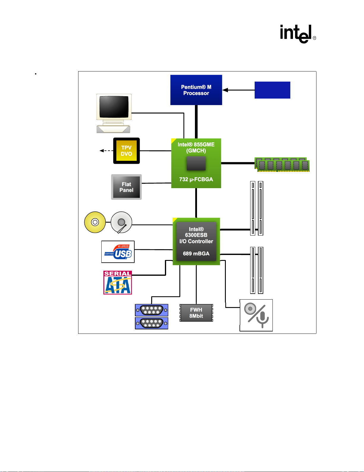
Intel® 855GME Chipset and Intel® 6300ESB ICH Embedded Platform Design Guide
System Overview
Figure 1. Embedd ed Intel® 855G M E Chipset System Block Diagram
CRT
TPV
DVO
Flat
Panel
DVO B/C
Interface
LVDS
Interface
2 Ultra ATA100
IDE Channels
4 USB
2.0 Ports
Pentium® M
Processor
400 MHz
Pentium® M
Processor
Bus
Intel® 855GME
(GMCH)
732 µ-FCBGA
266 MHz
Hub Interface 1.5
Intel®
Intel®
6300ESB
6300ESB
I/O Controller
I/O Controller
689 mBGA
689 mBGA
Voltage
Regulator
DDR
266/333
Up to 4 (66 MHz)
PCI-X Masters
2 SATA
150 Ports
Dual Integrated
16550 UARTs
26
LPC
Bus
FWH
8Mbit
Up to 4 (33 MHz)
PCI Masters
Audio
Page 27

Intel® 855GME Chipset and Intel® 6300ESB ICH Embedded Platform Design Gu ide
2.3 Component Features
2.3.1 Intel® Pentium® M Processor
2.3.1.1 Architectural Features
• On-d ie primary 32 Kbyte instruction cache and 32 Kbyte write-back data cache
• On-die 1 Mbyte second level cache
• Suppo rts Streaming SIMD Extens ions 2 (SSE2)
• Assisted Gunning Transceiver Logic (AGTL+) bus driver technology
• Enhanced Intel SpeedStep
multiple vol tage and frequency point s
• Supports host bus Dynamic Bus Inversion (DINV)
• Dynamic powe r down of data bus buffers
• BPRI# control to disable address/control buffers
2.3.1.2 Packaging/Power
®
technology to enable real-tim e dynamic switching between
System Overview
• 478-pin, Micro-FCPGA and 479-ball Micro-FCBGA packages
• VCC-CORE for Intel
to 0.956 V (lowest frequency mode); VCCA (1.8 V); VCCP (1.05 V)
• VCC-CORE for Low Voltage Intel
frequency mode) to 0.956 V (lowest frequency mode); VCCA (1.8 V); VCCP (1.05 V)
• TDP: 24.5 W for the Intel
• TDP: 12 W for the Low Voltage Intel
®
Pentium® M Processor at 1.6GHz: 1.484 V (highest frequency mode)
®
Pentium® M Processor at 1.1 GHz: 1.180 V (highest
®
Pentium® M Processor at 1.6 GHz
®
Pentium® M Processor at 1.1 GHz
2.3.2 Intel® Pentium® M Processor on 90 nm Process with 2 MB L2 Cache
All features of the Intel Pentium M processor are supported by the Intel Pentium M P rocessor on
the 90 nm process wi th 2 MB L2 ca che. The proces sors a lso uti li ze the s ame packa ge and f ootpr int.
This section only lists the additional on-die enhancements. For more details, see the I ntel Pentium
M Proce ssor on 90nm Process with 2 MB L2 Cache Datasheet.
New features on the Inte l P entium M Processor on the 90nm proce ss with 2MB L2 cache include:
• On-die 2-M B L2 ca ch e
• S tr ained silicon process technology
Voltage and Power Changes:
®
• Intel
Pentium® M Processor 745 (90 nm, 2 MB L2 Cache, 1.8 GHz, 400 MHz FSB):
—V
CC-CORE (HFM)
—V
CC-CORE (LFM)
—V
—TDP: 21 W
: 1.8 V only
CCA
: 1.276 V – 1.340 V
: 0.988 V
January 2007 27
Page 28

Intel® 855GME Chipset and Intel® 6300ESB ICH Embedded Platform Design Guide
System Overview
®
• Intel
Pentium® M Processor Low Voltage 738 (90 nm, 2 MB L2 Ca che, 1.4 GHz, 400 MHz
FSB):
—V
CC-CORE (HFM)
—V
CC-CORE (LFM)
—V
— TDP: 10 W
: 1.8 V and 1.5 V supported
CCA
: 1.052 V
: 0.956 V
2.3.3 Intel® Celeron® M Processo r
Most features of the Intel Pentium M processor are supported by the Intel Celeron M Processor.
For more details, see the Intel
Processor Features
• Pi n- compatible with the Intel
• 1.3 GHz operation, available in 478-pin micro FCPGA and 479-ball micro FCBGA packages
• On-die 512-KB second level cac he
• Voltage/Power Changes
— VCC-CORE for 1.3 GHz: 1.356V
— TDP for 1.3 GHz = 24.5 W
• No suppo rt for Enhanced Intel SpeedStep
Thermal Monitor 2.
®
Celeron® M Processor Datashee t.
®
Pentium® M processor.
®
Technology, Deeper Sleep operation, or Intel®
2.3.4 Intel® Celeron® M Processor on 90 nm process
Most features of the Intel Pentium M proc essor on 90 nm process with 2 MB L2 cache are
supported by the Intel Celeron M processor on 90nm process. For more details , see the Intel
Celeron
®
M Process or Datasheet on 90 nm process Datasheet.
®
• Intel
• Intel
Celer o n® M Processor 370 (90 nm, 1.5 GHz, 400 MHz FSB):
— On-die 1-MB L2 Cache
—TDP = 21 W
—V
— On- die 512-KB L2 Cache
—TDP = 5.5 W
—V
: 1.8 V and 1.5 V supported only
CCA
®
Celer o n® M Processor Ultra Low Voltage 373 (90 nm, 1.0 GHz, 400 MHz FSB):
: 1.8 V and 1.5 V supported
CCA
2.3.5 ULV Intel® Celeron® M Proce ssor at 600 MHz
Most features of the Inte l Celeron M processor are supported by the ULV Intel Celeron M at 600
MHz processor. For more details, see the Ultra Low Voltage Intel® Celeron® M Processor at 600
MHz Addendum to the Intel® Celeron® M Processor Datasheet.
®
28
Page 29

Intel® 855GME Chipset and Intel® 6300ESB ICH Embedded Platform Design Gu ide
System Overview
®
• Intel
Celeron® M Processor Ultra Low Voltage at 600 MHz (130 nm, 600 MHz, 400 MHz
FSB):
— On-die 512-KB L2 Cache
—TDP = 7 W
— VCC-CORE: 1.004 V
—V
— 479-ball micro FCBGA package
: 1.8 V supported
CCA
2.3.6 Intel® 855GME Chipset Graphics Memory Controller Hub (82855GME)
2.3.6.1 Intel® Pentium® M Processor/Intel® Celeron® M Proc essor Support
• Optimized for the Pentium M processor/ Celeron M processor in 478-pin micro-FCPGA and
479-ball micro-F CBGA package
• AGTL+ bus driver technology with integrated GTL termination resistors (gated AGTL+
receivers for re duced power)
• Suppo rts 32-bit AGTL+ bus addressi ng (no support for 36-bit address extension).
• Suppo rts Uni-processor (UP) systems.
• 400 MT/s Pentium M processor FSB support (100 MHz)
• 2X Addres s, 4X Data
• 12 deep in -order queue
2.3.6.2 Integrated System Memory DRAM Controller
• Suppo rts up to two double-sided DIMMs (four rows populated) with unbuffe red PC2100/
PC2700 DDR-SDRAM (with or without ECC)
• Suppo rts 64 Mbit, 128 Mbit, 256 Mbit and 512 Mbit technologies for x8 and x16 width
devices
• Maximum of 2 Gbytes system memory by using 512 Mbit technology devices (double side d)
• Suppo rts 266MHz, and 333 MHz DDR devices
• 64-bit data interface (72-bit with ECC)
• 2100/2700 system memory interface
• Suppo rts up to 16 simultaneous open pages
2.3.6.3 Internal Graphics Controller
• Graphics Core Frequency
— Display/Render frequency up to 250 MHz (with 1.35 V core voltage)
• 3D Graphic s Engine
— 3D Setup and Render Engine
January 2007 29
Page 30

Intel® 855GME Chipset and Intel® 6300ESB ICH Embedded Platform Design Guide
System Overview
— Zone Re ndering
— High quality performance Texture Engine
• Analog Display Support
— 350-MHz integrated 24-bit RAMDAC
— Hardwar e color cursor support
— Accompanying I2C and DDC channels provided through multiplexed interface
— Dual independent pipe for dua l independent display
— Si mul taneous displa y: same images and native display timings on each display device
• Digital V ideo Out Port (DVOB & DVOC) support
— DVOB & DVOC with 165-MHz dot clock s upport for each 12-bit interface
— Compliant with DVI Specification 1.5
• Dedic ated LFP (local flat panel ) support
— Single or dual channel LVDS panel support up to UXGA panel resolut ion with frequency
range from 25 MHz to 1 12 MHz per channel
— SSC support of 0.5%, 1.0%, and 2.5% center and down spread with externa l S S C cloc k
— Sup ports data format of 18 bpp
— LCD pan el power sequencing compliant with SPWG timing specification
— Compliant with ANSI/TIA/EIA –644-1995 spec
— Integra ted PWM interface for LCD backlight inverter control
— Bi-linear Panel fitting
• Interna l Graphics Features (855GME)
— Core Vcc = 1.2 V or 1.35 V (to support higher graphics core frequency and DDR333)
— Graphi cs core frequency
• Dis play core frequency at 133 MHz, 200 MHz, 250 MHz
• Render core frequency at 100 MHz, 133 MHz, 166 MHz, 200 MHz, 250 MHz
• Intel® Dual-Frequency Graphics Technology
— 3D Graphic s Engine
• Enhanced Hardware Binning Instruction Set supported
• Bi-Cubic Filtering supported
• Lin ear Gamma Blending for Video Mixer Rende ring (VMR)
• Video Mixer Rendering (VMR) supported
— Graphics Power Management
• • Dyna mic Core Frequency Switching
®
• Intel
Smart 2D Display Technology
• Memory Self-Refresh During C3
®
• Intel
Display Power Saving Technology
30
Page 31

Intel® 855GME Chipset and Intel® 6300ESB ICH Embedded Platform Design Gu ide
2.3.6.4 Packaging/Power
• 732-pin Micro-FCBGA (37.5 mm x 37.5 mm)
• VTTLF, VTTHF (1.05 V)
• VCC, VCCASM, VCCHL, VCCAHPLL, VCCAGPLL, VCCADPLLA, VCCADPLLB
(1.2 V or 1.35 V; as needed to support 250MHz graphics core frequency and DDR333)
• VCCADAC, VCCDVO, VCCDLVDS, VCCALVDS, (1.5 V)
• VCCSM, VCCQSM, VCCTXLVDS (2.5 V)
• VCCGPI O ( 3.3 V)
• Power Management (855GME)
— Optimized Clock Gating for 3D and Display Engines
— On-die thermal sensor
2.3.7 Intel® 6300ES B System Features
The Intel® 6300ESB I/O Controller Hub system consists of:
• The I/O Controller Hub (Inte l
subsystem with access to the rest of the system. Additionally, it integrates many I/O functions.
®
6300ESB I/O Controller Hub) which provides the I/O
System Overview
The Intel
®
6300ESB I/O Controller Hub integrates:
• Upstream Hub Interface for access to the MCH
• Two port Serial ATA controller
• Two channel Ultra ATA/100 Bus Master IDE controller
• One EHCI USB 2.0 host co ntroller and two UHCI USB 1.1 host controllers (expanded
capabilities for four ports)
• I/O APIC
• SMBus 2.0 controller
• FWH interface
• LPC interfac e
• AC’97 2.2 interface
• PCI-X 1.0 interface at 66MHz
• PCI 2.2 interface
• Two Serial I/O ports
• Two-Stage Watchdog timer
2.3.8 Firmware Hub (FWH)
• An integrated hardware Random Number Generator (RNG) on Intel parts
• Regi ster-based locking
January 2007 31
Page 32

Intel® 855GME Chipset and Intel® 6300ESB ICH Embedded Platform Design Guide
System Overview
• Hardware-ba sed locking
• Five GPIs
2.3.8.1 Packaging/Power
• 32-pin TS O P/PL CC
• 3.3-V core and 3.3 V/12 V for fast programming
32
Page 33

Intel® 855GME Chipset and Intel® 6300ESB ICH Embedded Platform Design Gu ide
General Design Cons iderations
General Design Considerations 3
This section documents motherboar d layout and routing guidelines for the Intel® 855GME/
6300ESB chipset platforms. It does not discuss the functional aspects of any bus or the la yout
guidelines for an add-in device.
When the guidelines lis ted in this document are not followed, it is very important that thorough
signal integrity and timing simulations are completed for each design. E ven when the guidelines
are followed, Intel recommends that critical signals be simulated to ensure proper s ignal integrity
and flight time . Any deviation from the guidelines shall be simulated.
The trace impedance typically noted (i.e., 55 Ω ± 15 percent ) is the nomin al trace impedance for a
5 m il wi d e ex ternal trace and a 4 mil wide internal trace. How ev e r, some st ack-ups may lead to
narrower or wider traces on internal or external layers in order to meet the 55 Ω impedance target.
That is, the impedance of the trace when not subje cted to the fields creat ed by changing current in
neighboring traces. No te the trace impedance target assumes that the trace is not subjected to the
EM fields created by changing current in neighboring traces. It is important to consider the
minimum and maximum impedance of a trace based on the switching of neighboring traces when
calculating flight times. Using wider spaces between the tra ce s may minim ize this trace-to-trace
coupling. In addition, these wid er s paces reduce settl ing time.
Coupling between two trac es is a function of the coupled length, the distance separating the traces,
the signal edge rate, and the degree of mutual capacita nc e and inductanc e. In order to minim ize the
effects of trace-to-trace coupling, the routing guidelines documented in this se ction shall be
followed. Also, al l high-speed, impedance-controlled si gnals (e.g., Intel
FSB signals) shall have continuous GND referenced planes and cannot be routed over or under
power/GND plane splits.
3.1 Nominal Board Stack-Up
The Intel 855GME /6300ESB chipset-based platforms require a board stack-up yielding a target
impedance of 55 Ω ± 15n percent. An e xample of an 8-laye r board stack-up is shown in Figure 2.
The left side of the figure illustrates the starting dimens ions of the metal and dielec tr ic materia l
thickness as well as drawn trace width dimensions prior to lamination, conductor plating, and
etching. After the motherboard materials are laminated, condu ctors plated, and etched, somewhat
different dimensions resul t. Dielectric mate rials become thinne r, under/over etching of conductors
alters their trace width, and conductor pla ting makes them thicker.
Note: For the purpose of extracting electrical models from transmission line properties, the final
dimensions of signals after lamina tion, plating, and etching should be used.
The stack-up us es 1.2-mil (1 oz.) copper on power planes to reduce I*R drops and 0.6-mil c opper
thickness on the outer signal layers: pri mary side layer (L1), and second ary s ide layer (L8).
Additionally, 1.2-mil copper th ic kness is us ed on t he i nterna l sig nal la yers: Layer 3 (L3 ), and L ayer
6 (L6). After plating, the external layers bec ome 1.2 to 2 mils thick.
®
Pentium® M processor
January 2007 33
Page 34

Intel® 855GME Chipset and Intel® 6300ESB ICH Embedded Platform Design Guide
CORE
General Design Cons i derations
To meet the nominal 55Ω characteristic impeda nce primary and secondary side layer micro-strip
lines are drawn at 5 mil trace widt h but end up with a 4 mil final trace width after etching. For the
same reason, th e 5 mil thick prepreg between t he primary si de layer and Laye r 2 start s at 5 mils but
becomes 4.5 mils after lami nation. This situation and result als o applies to Layer 7 and the
seco nd ary si de layer.
To ensure impedanc e con trol of 55 Ω, the primary and secondary side laye r mi cro-strip lines shall
reference solid ground pla nes on Layer 2 and Layer 7, respectively.
Figure 2. Recommend ed B oa r d Stack- up Dim e nsions
Dielectric Layer Layer Copper Trace Trace
Stackup
S
PRE PRE G
P2PLANE1
CORE
S3SIGNAL1455
PRE PRE G
P4PLANE1
CORE
P5PLANE1
PRE PRE G
S6SIGNAL1455
P7PLANE1
PRE PRE G
S
Thickness No. Type We ight Width Impedance
(mills)
1 SIGNAL 1/2+plating 5 55
>3
>5
>5
>28
>5
>5
>3
8 SIGNAL 1/2+plating 5 55
(oz) (mils) (ohms)
Internal s ignal traces on Layer 3 and Layer 6 are unbalanced strip-lines. To meet the nominal 55 Ω
characteris tic impe dance for these trac es, they refere nce a soli d ground plane on Layer 2 and Layer
7. Because the coupling to Layer 4 and Layer 5 is still si gnificant, (especially true when thinner
stack-ups use balanced strip-lines on internal layers) these layers are converted to ground floods in
the areas o f the mot h er b o ar d w he r e th e sp ee d - cr i ti cal inter fa c es such as the Intel P e nt i um
M/Celeron M Processor FSB or DDR system memory are routed. In the remaining sections of the
motherboard layout the Layer 4 and Layer 5 layers are used for power delivery.
For 55 Ω characteristic impedance Layer 3 (Layer 6), strip - lines have a 4 mil final trace width and
are separated by a core dielectric thickness of 4. 8 mils after la mination from the La yer 2 (Layer 7)
ground plane and 4. 8 mil thickness prepreg after lamination to separate it from Layer 4 (Layer 5).
The starti ng thickness of these core and prepreg dielectric layers before lamination is 5 mils and 5
mils, respectively.
The secondary side layer (L8) is also used for power delive ry in many ca ses since it benefits from
the thick c opper plating of the external layer plating as well as refer encing the clos e (3 mil prepreg
thickness) Layer 7 ground plane. The benefi t of such a stack-up is low inducta nce power delivery.
34
Page 35

Intel® 855GME Chipset and Intel® 6300ESB ICH Embedded Platform Design Gu ide
3.2 Alternate Stack-Up s
Designers may choose to use different stack-ups (number of layers, thi ckness, trace width , et c.)
from the one ex am ple ou tline d in Figure 2. However, the followi ng key elements shal l be observe d:
1. Final post lamination, post etching, and post plating dimensions shall be used for electric al
model extractions.
2. Power plane layers shall be 1 oz. thick and the outer signal layers shall be ½ oz. thick, while
the internal signal layers shall be 1 oz. thick. External layers become 1 – 1.5 oz. (1.2 – 2 mils)
thick after plating.
3. All high-speed signals shall reference solid ground planes through the length of their routing
and shall not cross plane splits. To ensure this, both planes surrounding strip-lines shall be
GND.
4. Intel recommends that high-speed signal routing be done on internal , strip-line layers.
5. For high-speed signals transitioning between layers next to the component, the signal pins
shall be acc ounted for by the GND stitching vias that would stitch all the GND plan e layers in
that area of th e motherboard. Due to the arrange me nt of the Intel Pentium M/Celeron M
Processor and Intel 855GME chipset Graphics Memory Controller Hub (82855GME)
pin-maps, GND vias placed ne ar all GND lands are also very close to high-speed signals that
may be tr ans itioning to an internal layer. Thus, no addition al ground stitching vias (besid es the
GND pin vias) are required in the imm ediate vicinity of the Intel Pentium M/Celeron M
Processor and 82855GME packages to accompany the signal transitions from the component
side into an internal layer.
General Design Cons iderations
6. High-speed routing on e xternal layers shal l be minimized in order to avoid EMI. Routing on
external layers also introduces diff er ent delays compared to internal layers. This makes it
extremely difficult to do length matching when some routing is done on both internal and
external layers.
7. When Intel’s recommended stackup guidel ines are not used, the desi gner is liable for all
aspects of their board design (i.e., understanding impacts of SI and power distribution).
January 2007 35
Page 36

Intel® 855GME Chipset and Intel® 6300ESB ICH Embedded Platform Design Guide
General Design Cons i derations
36
Page 37

Intel® 855GME Chipset and Intel® 6300ESB ICH Embedded Platform Design Gu ide
®
Pentium® M/Cel eron® M Processor FSB Design and Power Delivery Guidelines
Intel
Intel® Pentium® M/Celeron® M
Processor FSB Design and Power
Delivery Guidelines 4
The following layout guidelines support designs using th e Intel® Pentium® M/Celeron® M
Processor and the Intel
on-die Rtt resi stors on both the processor and the chipset, additional resistors do not need to be
placed on the motherboard for most Intel Penti um M/C eleron M Processor FSB signals. A simple
point-to-po int interconnect topology is used in these cases.
®
855GME chipset Graphics Memory Controller Hub (82855GME). Due to
4.1 Intel® Pentium® M/Celeron® M Processor FSB Design Recommendations
For proper operatio n of the Inte l Pentium M/Cele ron M Proce ssor and t he Intel 855GME chips et, it
is necessary that the syste m designer meet the timing and vol tage spec ifi cati on of each compone nt.
The following recomme ndations are Intel’s best guidelines based on extensive simulation and
experimentation that make assumptions, which may be dif f erent from an OEM’s system desi gn.
The most accurate way to understand the signal integrity and timing of the Intel Pentium
M/Celeron M Processor FSB in your platform is by performing a comprehensive simulation
analysis. It is possible that adjustments to trace impedance, line length, termination impedance,
board stack-up, and other parameters may be made that improv e sy st em performance.
Refe r to th e latest Intel
90nm Process with 2MB L2 Cache Datasheet, or Intel
FSB signal list , s ignal types, and definitions. Below are the design recommendations for the data,
address, and strobes. For the following discussion, the pad is defined as the attach point of the
silicon die to the package substrate. The following topology and layout guidelines are preliminary
and subj ect to chan g e . The guidelines a re derive d fr om empiri ca l testing with GM C H pac k age
models.
®
Pentium® M Processor Datasheet , Intel® Pentium® M Processor on the
®
Celeron® M Processor Datasheet for a
4.1.1 Recommended Stack-Up Routing and Spacing Assumptions
The following section describes in more detail, the terminology and definitions used for diffe r ent
routing and stack-up assumptions that a pply to the recommended mother board stack-up shown in
Section 3.1 .
4.1.1.1 Trace Space to Trace – Reference Plane Separation Ratio
Figure 3 illustrates the recommended rel ationship between the edge-to-edge trace spac ing (2X)
versus the trace to ref ere nce plane separation (X). An edge-to-edge trace spacing (2X) to
trace – reference plane se paration (X) ratio of 2:1 ensures a low cross talk coefficie nt. All the
January 2007 37
Page 38

Intel® 855GME Chipset and Intel® 6300ESB ICH Embedded Platform Design Guide
®
Pentium® M/Celer on® M Processor FSB Design and Power Delivery Guidelines
Intel
effects of crosstalk are difficult to simulate. The timing and layout guidel ines for the Intel Pentium
M/Celeron M Processor have been created wit h the assumption of a 2:1 trace spa cing to reference
plane ratio. A smaller ratio has an unpredicta ble impact due to crosstalk.
Figure 3. Trace Spacing versus Trace to Reference Plane Example
Reference Plane (V SS)
X
Trace
2X
Trace
4.1.1.2 Trace Space to Trace Width Ratio
Figure 3 illustrates the recommended relationship between the edge-to-edge trace spacing versus
trace widt h ratio for the best signal quality results. In general, a 3:1 trace space-to-trace width ratio
(shown in F igure 5) is preferred and highly recom mended. In case of routing difficulties on the
motherboard, us ing a 2:1 ratio (shown in Figure 4) would be acc eptable only if additional
simulation s conclude tha t it is possib le, whi ch may i nclude some change s to the sta ck-up or rout ing
assumptions.
Figure 4. Two-to-One Trace Spacing-to-Trace Width Example
2X
Trace
Figure 5. Three-to-One Trace Spacing-to-Tr ace Width Example
3X
Trace
4.1.1.3 Recommended Stack-up Calculated Coupling Model
The imp ort an ce of main t ai ni n g an ad e qu a te trace sp ac e to tr ac e w id t h ra t io is to ac hi ev e th e be s t
signal quality possible given routing constraints. The simulations performed that resulted in the
recommended 3:1 trace spacing to trace width ratio are to keep the coupling between adjacent
traces below a maximum value. For the recommended stack-up, the constants shown in Figure 2
are assu med to be co ns tant for a typical stack-up. This me ans the mutual to se lf -coupling
Trace
X
Trace
X
38
Page 39

Intel® 855GME Chipset and Intel® 6300ESB ICH Embedded Platform Design Gu ide
il
il
®
Pentium® M/Cel eron® M Processor FSB Design and Power Delivery Guidelines
Intel
relations hip given below does not take into account the normal tolerances that are allowed for in
the recommended board stack-up’s parameters. For the re commended stack-up shown in Figure 2,
the calculated capacitive coupling maximum value is represented by the follo wing relationship:
(C
MUTUAL/CSELF
) x 100 = 8.15%
As sh own in Figure 6, the coupling values are calculated based on a three- line model, represen ted
by Trace 1, Trace 2, and Trace 3. Based on the capac itive coupling model shown, the
aforementioned parameters are:
C
MUTUAL
C
SELF
= C21 + C23
= C22 (Trace 2, i.e., CS2a + CS2b)
When a stack-up that is employed does not adhere to the recommended stack-up, a new extraction
must be made for the stack-up us ing a 2D fie ld s olver program. According to the 2D field solver
results, new coupling calculations must be performed to ensure that the coupling results are less
than the aforementioned capacitive coupling maxim um value of 8.15 percent . When the coupling
results are greate r than the maxim um va lue, a dditi onal s yste m-level simula tio ns must be perfo rmed
to avoid any signal quality issues due to crosstalk effects.
Figure 6. Recom mend ed Stack-up Capacitive Coupling Model
GND
CS2aCS1a
C21
Trace 1 Trace 2
C23
CS3a
11.2 M
Trace 3
CS1b
CS2b
CS3b
4.8 M
GND
Note: CS1a + CS1b = C11
CS2a + CS2b = C22
CS3a +CS3b = C33
4.1.1.4 Signal Propagation Time-to-Distance Relationship and Assumptions
Due to the high-frequency nature of some interface s and signals, lengt h matching may or may not
exist as part of the routing requirements for a given interface. In general, the tolerance s that
specific signals in a bus must be routed to are stated as a length measured in mils or inches and are
specific to the recommended motherboard stack-up (refe r to Section 3.1). However, some length
matching tolerances for signals listed in this design guide may be state d as a measurement of time.
In such cases, the correlation of the period of time to an actual length value depends on board
stack-up.
Based on the recommended stack-up, the sign al propagation time to distance relationship, for the
purpose of this des ign guide, is as follows:
• S trip-line (internal layer) routing: 180ps for 1.0 inch
January 2007 39
Page 40

Intel® 855GME Chipset and Intel® 6300ESB ICH Embedded Platform Design Guide
®
Pentium® M/Celer on® M Processor FSB Design and Power Delivery Guidelines
Intel
For example, a length-matching requirement of ± 50 ps for routing on a strip-line (internal) layer
would correlat e to a trace length whose tole rance are ± 278 mils of an associated trace. The signal
propagation time-to-distance relationship listed abo ve is based on a single transmission line model
incorporati ng a typical stack-up. Thus, no other signals or tr aces are accounted for in such a model
and there is an assumpt ion of zero coupling with othe r traces. Also, the recommended stack-up’s
parameter tolerances are not taken into a ccount in the typical stack-up assumpti ons. Finally, in
cases that need to accou nt for worst-case stack-up parameters and for even- or odd mode coup ling,
new extractions from the stack-up model must be done to provide an accurate signal propagation
time-to-distance relationship.
4.1.2 Common Clock Signals
All common clock signals use an AGTL+ bus driver technology with on- die integrated GTL
termination resistors connected in a point-to-point, Zo = 55 Ω, co ntr olled impedance topology
between the Intel Pentium M/Celeron M Processor and the GMCH. No external termination is
needed on th ese signals. These signals operate at the Intel Pentium M/Celer on M Processor FSB
freq uency of 100 MHz.
Common clock signals shall be routed on an intern al layer while referenci ng solid ground planes.
Based on current simulation results, routing on internal lay ers allows for a minimum pin-to-pin
motherboard length of 1.0 inch and a maximum of 6.5 inches. Trace length matching for the
common clock signals is not required. For details on minimum motherboard trace length
requirements, refer to Section 4.1.2.1 and Table 3 for more details. Intel recommends rout ing these
signals on the same internal layer for the entire length of the bus. When routing c ons traints require
routing of the se sign als wit h a transi tio n to a dif f erent l ayer, a minimum of one ground stitchi ng via
for every two signa ls shall be placed within 100 mils of the signal transition vias.
Routing of the common clock signals shall use 2:1 trace spacing to trace width. This implies a
minimum of 8 mils spacing (i.e., 12 mil minimum pitch) for a 4 mil trace width for routing on
internal layers. Practical cases of escape routing under the 82855GME or Intel Penti u m M/Celeron
M Processor package outline and vici nity may not allow the implementation of 2:1 trace spacing
requirements. Although every attempt shall be m ade to maximi ze the signal spacing in these areas,
it is allo wable to have 1:1 t race s paci ng underne ath the GMCH and th e Intel Penti um M/Celer on M
Processor package outlines and up to 200–300 mils outside the package outline.
Table 3 summarizes the list of common clock and key routing requirements. RESET#
(CPURESET# of GMCH) is also a common clock signal but require s a special treatment for the
case where an ITP700FLEX debug port is used. Refer to Section 4.1. 6 for further details.
Table 3. Intel
Common Clock Signal Internal Layer Routing Guideline s (Sheet 1 of 2)
† For topologies where an ITP700FLEX debug port is implemented, refer to Section 4.1.6 for RESET#
®
Pentium® M/Celeron® M Processor System Bus
Signal Names
CPU GMCH
ADS# ADS # Str ip-line 997 6.5 55 ± 15% 4 and 8
BNR# BNR# Stri p-line 12 98 6.5 55 ± 15% 4 and 8
BPRI# BPRI# Strip-line 1215 6.5 55 ± 15% 4 and 8
BR0# BR0# Strip-line 1411 6.5 55 ± 15% 4 and 8
(CPURESET#) impl eme ntat io n details .
T ransmission L ine
Type
Tota l Trace L ength
Min
(mils)
Max
(inches)
Nominal
Impedance
(Ω)
Width and
Spacing
(mils)
40
Page 41

Intel® 855GME Chipset and Intel® 6300ESB ICH Embedded Platform Design Gu ide
®
Pentium® M/Cel eron® M Processor FSB Design and Power Delivery Guidelines
Intel
Table 3. Intel® Pentium® M/Celeron® M Processor System Bus
Common Clock Signal Internal Layer Routing Guidel ines (Sheet 2 of 2)
Signal Names
CPU GMCH
DBSY# DBSY# Strip-line 1159 6.5 55 ± 15% 4 and 8
DEFER# DEFER# Strip-line 12 91 6.5 55 ± 15% 4 and 8
DPWR# DP W R # Strip-lin e 1188 6.5 55 ± 15% 4 and 8
DRDY# DRDY# Strip-line 1336 6.5 55 ± 15% 4 and 8
HIT# HI T# Strip-li n e 13 03 6.5 55 ± 15 % 4 and 8
HITM# HITM# Strip-l ine 1203 6.5 55 ± 15% 4 and 8
LOCK# HLOCK # Strip-lin e 1198 6.5 55 ± 15% 4 and 8
RS0# RS0# Strip-line 13 15 6.5 55 ± 15% 4 and 8
RS1# RS1# Strip-line 1193 6 .5 55 ± 15 % 4 and 8
RS2# RS2# Strip-l in e 1247 6.5 55 ± 15 % 4 and 8
TRDY# HTRDY# Strip-line 1312 6.5 55 ± 15% 4 and 8
†
RESET#
† For topol ogies where an ITP 700FLEX debug po rt is impl emented, refer to Section 4.1.6 for RESET#
(CPUR ESET#) i m plementation details.
CPURESET# Stri p-l in e 1101 6.5 55 ± 15% 4 and 8
Transmission Line
Type
T otal Trace Length
Min
(mils)
Max
(inches)
Nominal
Impedance
(Ω)
Width and
4.1.2.1 Intel® Pentium® M/Celeron® M Processor Common Clock Signal
Package Length Compensation
Spacing
(mils)
Trace length matching for the common clock signals is not required. However, package
compensation for the c ommon cl ock signals is required for the minimum board trace. Refer to
Table 4 and the example for m ore details. Package length compensation shall not b e confused with
length matching. Length matching refers to constraints on the minimum and maximum length
bounds of a signal gro up base d on clock l ength, whereas pac kage lengt h compe nsati on refers to the
process of adjusti ng out package length variance across a signal group .
All common clock signals are required to meet the minimum pad-to-pad requirement of 2.212
inches, based on ADS# (as this signal has the longest package lengths) implies a minimum
pin-to-pin mothe r board trace length of 1.0 inches or more depending on package lengths. As a
result, additional motherboard trace is added to some of the shorter common clock nets on the
system board in order to meet the longes t common clock s ignal tot al trac e lengths from the die-pa d
of the processor to the associated die-pad of the chipset.
For example:
ADS# = 997 mils board trace + 454 Intel Pentium M/Celeron M Process or PKG + 761 GMCH
PKG = 2212 pad-to-pad length.
BR0# = X mils board trace + 465 Intel Pentium M/Celeron M Processor PKG + 336 GMCH PKG
= 2212 pad-to-pad length.
Therefore: BR0# boa rd t race = 2212 pad- to-pad l ength - 46 5 Int el Penti um M/Ce le ron M Proces sor
PKG - 336 GMCH PKG = 1411 pin-to-pin length.
January 2007 41
Page 42

Intel® 855GME Chipset and Intel® 6300ESB ICH Embedded Platform Design Guide
®
Pentium® M/Celer on® M Processor FSB Design and Power Delivery Guidelines
Intel
Figure 7 depicts the common cloc k topology.
Figure 7. Common Clock Topology
Table 4. Intel
Signal Package Lengths and Minimum Board Trace Lengths
Processor
Pad
Length L1
Package trace
Motherboard PCB trace
®
Pentium® M/Celeron® M Processor and Intel® GMCH FSB Common Clock
Signal Names Package Length
CPU GMCH CPU GMCH
ADS# ADS# 454 761 2212 997
BNR# BNR# 506 408 2212 1298
BPRI# BPRI# 424 573 2212 1215
BR0# BR0# 336 465 2212 141 1
DBSY# DBSY# 4 45 608 2212 1159
DEFER# DEFER# 349 572 2212 1291
DPWR# DPWR# 506 518 2212 1188
DRDY# DRDY# 529 347 2212 1336
HIT# HIT# 420 489 2212 1303
HITM# HITM# 368 641 2212 1203
LOCK# HLOCK # 499 515 2212 1198
RS0# RS0# 576 321 2212 1315
RS1# RS1# 524 495 2212 1193
RS2# RS2# 451 514 2212 1247
TRDY# HTRDY# 389 511 2212 1312
RESET# CPURESET# 455 656 2212 1101
GMCH
Pad
Total Pad-to-Pad Min.
Length Requirements L1
Minimum
Routable Board
T r ace Length
4.1.3 Source Synchronous Signals General Routing Guidelines
All source synchronous signals use an AGTL+ bus driver technology with on-die GTL termination
resistors connect ed in a po int-to-p oint , Zo = 55 Ω controlled im pedanc e topol ogy betwe en th e Intel
Pentium M/Cel eron M Processor and the GMCH. No external te rmination is needed on these
signals. Source synchronous Intel Pentium M/Celeron M Processor FSB a ddress signals operate at
a double-pumped rate of 200 MHz while the source synchronous proc essor FSB data signals
operate at a quad-pu mped rate of 400 MHz. High speed operation of the source sync hronous
signals requires careful atte ntion to their routing considerations. The following guide lines shall be
strictl y adhe red to, to ensure robust high-frequency operat ion of these signals.
42
Page 43

Intel® 855GME Chipset and Intel® 6300ESB ICH Embedded Platform Design Gu ide
L5
L6
L7
®
Pentium® M/Cel eron® M Processor FSB Design and Power Delivery Guidelines
Intel
Source synchrono us da ta and address signals and their associated strobes are partitioned into
groups of signals. F light time skew minimization within the same group of s ource synchronous
signals is a key parameter tha t allows their high-frequency (400 MHz) operation. All the source
synchronous signals that belong to the sa me group shall be routed on the same internal layer for
the entire length of the bus. It is permissible to split different groups of source synchronous signals
between diff erent m otherboa rd layer s as lon g as all the signal s that belo ng to tha t group are kept on
the same layer. Grouping of the Intel Pentium M/Ce leron M Processor FSB source sync hronous
signals is summarized in Table 5 and Table 7. This practice results in a significant reduction of the
flight time skew beca use t he diel ectri c thic knes s, li ne width, and ve locit y of th e sign als are u nifor m
across a single layer of the stack-up. The relationship of dielectric thickness, line width, and
velocity between layers cannot be ensured.
The source synchronous signals shall be rout ed as a strip-line on an interna l layer with complete
reference to ground planes both above and below the si gnal layer. Routing with references to split
planes or power planes other than ground is not allowed. For the recommended stack-up example
as shown in Figure 2, source synchronous Intel Pentium M/Cele ron M Processor FSB signals are
routed on Layer 3 and Layer 6. Layer 2 and Layer 7 are solid grounds acr oss the entire
motherboard. However, this is not suffi cient because sign ificant coupling exists between sig nal
layer, Layer 3 and power plane Layer 4 as well as signal la yer, Layer 6 and power plane Layer 5.
To ensure complete ground re ferencing, Layer 4 a nd Layer 5 are converted to ground plane floods
in the areas where the source synchronous processor FSB signals ar e routed. In addition, all the
ground plane area s are stitched with ground vias in the vicinity of the Intel Pentium M/Celeron M
Processor and Intel 855GME c hipset package out lines with the vias of the ground pins of the Intel
Pentium M/Celeron M Processor and Inte l 855GME chipset pin-map.
Figure 8 illustrates a motherboard layout and a cross-sectional view of the recommended stack-up
of the Intel Pentium M/Celeron M Processor FSB so urce synchronous DATA and ADDRESS
signals referenc ing ground planes on both Layer 7 and Layer 5. In the socket cavity of the Intel
Pentium M/Cele ron M Pro cessor, Layer 5 and Layer 6 are used for VCC core power delivery.
However, outside the socket cavity Layer 6 signals are routed on top of a solid Layer 7 ground
plane and also Layer 5 is conve rted to a ground flood under the s hadow of the Intel Pentium
M/Celeron M Processor FSB signals routing between the Intel Pent ium M/Celeron M Processor
and GMCH. Stitching of all the GND planes is provided by the ground vias in the pin-map of the
Intel P e n t iu m M/Ce le r on M Processor an d GM CH.
®
Figure 8. La yer 6 Intel
Signals GND Referencing to Layer 5 and Layer 7 Ground Planes
L6 and L5 top side
Pentium® M/Celeron® M Processor FSB Source Synchronous
VCC
Stackup c ross - section
view
L4
FSB DATA
FSB ADDRESS
GND
GND
VCC
January 2007 43
Page 44

Intel® 855GME Chipset and Intel® 6300ESB ICH Embedded Platform Design Guide
®
Pentium® M/Celer on® M Processor FSB Design and Power Delivery Guidelines
Intel
Figure 9. Laye r 6 Intel® Pentium® M/Celeron® M Process or FSB Sourc e S y nchronous
Data Signals
Layer 6
FSB Data Signals
44
Page 45

Intel® 855GME Chipset and Intel® 6300ESB ICH Embedded Platform Design Gu ide
®
Pentium® M/Cel eron® M Processor FSB Design and Power Delivery Guidelines
Intel
Figure 10. Layer 6 Intel
Source Synchronous Address Signal s
®
Pentium® M/Celeron® M Processor System Bus
Layer 6
FSB Address Signals
In a similar way, Figure 11 illustrates a recommended layout and stack-up example of how an other
group of Intel Pentium M/Celeron M Processor FSB sourc e synchronous DATA and ADDRESS
signals may reference ground planes on both Layer 2 and Layer 4. In the sock et cavity of the Intel
Pentium M/Cele ron M Processor, Layer 3 is used for VCC core power delivery to reduce the I*R
drop. However, outside of the socket cavity, Layer 3 signals are routed below a solid Layer 2
ground plane. Layer 4 is converted to a ground flood under the shadow of the Intel Pentium
M/Celeron M Process or FSB signals routing betwe en the Pentium M/Celer on M processor and
GMCH. Figure 12 and Figure 13 depict example routing for Intel customer reference board.
January 2007 45
Page 46

Intel® 855GME Chipset and Intel® 6300ESB ICH Embedded Platform Design Guide
FSB
®
Pentium® M/Celer on® M Processor FSB Design and Power Delivery Guidelines
Intel
Figure 11. Layer 3 Intel® Pentium® M/Celeron® M Processor FSB Source Synchronous
Signals GND Referencing to Layer 2 and Layer 4 Ground Planes
L3 and L4 top side vi ew
VCC
Stackup cross - section
L2
L3
L4
GND
GND
FSB
100 MHz Clocks
Figure 12. Layer 3 Intel® Pentium® M/Celeron® M Processor FSB Source Synchronous
Data Signals
Layer 3
FSB Data
Signals
VCC
46
Page 47

Intel® 855GME Chipset and Intel® 6300ESB ICH Embedded Platform Design Gu ide
®
Pentium® M/Cel eron® M Processor FSB Design and Power Delivery Guidelines
Intel
Figure 13. Layer 3 Intel
Address Signals
®
Pentium® M/Celeron® M Processor FS B S ource Synch ronous
Layer 3
FSB Address
Skew minimization requires pin-to-pad trace length matching of the Intel Pentium M/Celer on M
Processor FSB source synchronous signals that belong to the same group including the strobe
signals of that group. Refer to Section4.1.2.1 for tr ace length matching and package
compensations requirements.
Current simulation results prov ide routing guidel ines using 3:1 spacing for the Intel Pentium
M/Celeron M Processor FSB sourc e synchronous data and strobe signals. This implies a minimum
of 12 mil spacing (i.e., 16 mil minimum pitc h) for a 4 mil trace width. Practical ca ses of escape
routing under the GMCH or Intel Pentium M/Celeron M Processor package outline and vicinity
may not even allow the implementation of 2:1 trace spacing requirem ents. Although every attempt
shall be made to maxi mize the signal spacing in these areas, it is allowable to have 1:1 trace
spacing und erneat h the GMC H and the Int el Pent ium M/C eleron M Proc essor pa ck age out lin es and
up to 200 – 300 mils outside the pac kage outline. The benefits of additional spacing include
increased signal quality and voltage margining. The trace routing and length matching
requirements are as fol lows in Section 4.1.3.1 to Section 4.1.3.3.
4.1.3.1 Source Synchronous – Data Group
Robust opera tion of the 400 MHz, source synchronous data signals require tight skew control. For
this reaso n, th ese s ign als are sp lit into mat ched group s as out lin ed in Table 5. All the signals within
the same group shall be kept on the same layer of motherboard routing and shal l be routed to the
same pad-to-pin length within ±100 mils of the associated strobes. Only the Intel Pentium
M/Celeron M Process or has the package trace equa liza tion for s ignal s withi n each da ta and addre ss
group. The GMCH does not have package trace equalizat ion for s ignals within each data and
address group. All sig nals shall be routed on the system board to meet the pad-to-pin matching
requirement of ± 100 mils. Refer to Table 9 for th e Intel 8 55 G ME chi p s e t packa ge len gths .
January 2007 47
Page 48

Intel® 855GME Chipset and Intel® 6300ESB ICH Embedded Platform Design Guide
®
Pentium® M/Celer on® M Processor FSB Design and Power Delivery Guidelines
Intel
Refer to Section 4.1.2.1 for trace length and package compensation requirements. The two
complementar y s trobe signals associated with each group shall be length matched (pad-to-pin) to
each other within ± 25 mils and tuned to the average length of the data signals (pad-to-pin) of their
associated group. This opti mizes setup/hold time margin.
®
Table 5. Intel
Pentium® M/Celeron® M Processor FSB Data Source Synchronous Signal
Trace Length Mismatch Mapping
Data Group
D[15:0]# DINV0# ± 100 mils DSTBP0#, DSTBN0# ±25 mils 1, 2
D[31:1 6]# DINV1# ± 100 mils DSTBP1#, DSTB N1# ± 25 mils 1, 2
D[47:3 2]# DINV2# ± 100 mils DSTBP2#, DSTB N2# ± 25 mils 1, 2
D[63:4 8]# DINV3# ± 100 mils DSTBP3#, DSTB N3# ± 25 mils 1, 2
NOTES:
1. Strobes of the same group shall be trace length matched to each other within ± 25 mils and to the average
length of their associated data signal group.
2. All length matching formulas are based on GMCH die-pad to Intel Pentium M/Celeron M Processor pin
total length per byte lane. Package length tables are provided for all signals to facilitate this pad-to-pin
matching.
DINV Signal for
Associated
Data Group
Signal
Matching
Data Strobes
Associated with the
Group
Strobe
Matching
Table 6 lists the source s ynchronou s dat a signal genera l routing re quirem ents. Due to th e 40 0 MHz,
high-frequency operation the data signals shal l be limited to a pin-to-pin tra ce length minimum of
0.50 inches and maximum of 5.5 inches.
Table 6. Intel® Pentium® M/Celeron® M Processor System Bus Source Synchronous
Data Signal Routing Guidelines
Signal Names
Data Group #1 Data Group #2 Data Group #3 Data Group #4
Trans-
mission
Line Type
Total Trace Length
Min
(inches)
Max
(inches)
Nominal
Impedance
Notes
Width
and
(
Ω)
spacing
(mils)
D[15:0]# D[31:16]# D[47:32]# D[63:48]# Strip-line 0.5 5.5 55 ± 15% 4 and 12
DINV0# DINV1# DINV2# DINV3# Strip-line 0.5 5.5 55 ± 15% 4 and 12
DSTBN[0]# DSTBN[1]# DSTBN[2]# DSTBN[3]# Strip-line 0.5 5.5 55 ± 15% 4 and 12
DSTBP[0]# DSTBP[1]# DSTBP[ 2]# DSTBP[3]# St rip-line 0.5 5.5 55 ± 15% 4 and 12
4.1.3.2 Source Synchronous – Address Group
Source sync hronous address signals operate at 200 MHz. Thus, their routi ng requirements are very
simila r to th e d at a sig n als. Ref e r to Section 4.1.3 and Section 4.1.3.1 for further details. Table 7
details the partition of the address s ignals into matche d length groups. Due to the lower operating
frequency of the address signals, pad-to-pin length matching is relaxed to ± 200 mils. Each group
is associated with only on e strobe signal. To m aximize setup/hold time margin, the address strobes
shall be trace length matched to the ave rage trace length of the address signals of their associ ated
group. In addi tion, each address signal shall be trace length matched wit hin ±200 mils of its
associated strobe sig n al.
48
Page 49

Intel® 855GME Chipset and Intel® 6300ESB ICH Embedded Platform Design Gu ide
Intel
Table 7. Intel
Signal Trace Length Mismatch Mapping
®
Pentium® M/Cel eron® M Processor FSB Design and Power Delivery Guidelines
®
Pentium® M/Celeron® M Processor FSB Address Source Synchronous
CPU Signal Name
REQ[4:0]#, A[16:3]# ± 200 mils ADSTB0# ± 200 mils 1, 2, 3
A[31:17]# ± 200 mils ADSTB1# ± 200 mils 1, 2, 3
NOTES:
1. ADSTB[1:0]# shall be trace length matched to the average length of the associated address signals group.
2. Each address signal shall be trace leng th matched to its associated address strobe wi thin ± 200 mils.
3. All length matching formulas are based on GMCH die-pad to Pentium M/Celeron M processor pin total
length per sign al group. Package length tables are provided for all signals to facilitate this pad to pin
matching.
Signal
Matching
Strobe Associated with the
Group
Strobe to Associat ed
Addres s Signal
Matching
Table 8 lists the source synchronous address signals gene ral routing requireme nts . They should be
routed to a pin-to-pi n length minimum of 0.50 inches and a maximum of 6.5 inches. Due to the
200 MHz, high-frequency operation of the address signals, th e routing guidelines lis ted in Table 8
allow for 2:1 spacing for the address signals given a 55 Ω ± 15% characteristic trace impedance
except for address strobe signals. But if sp ace permits, 3:1 spaci ng is strongly advised for thes e
signals.
Table 8. Intel® Pentium® M/Celeron® M Process or FSB Sourc e Synchron ou s
Address Signal Routing Guidelines
Signal Names
Address
Group #1
A[16:3]# A[31:17]# Strip-line 0.50 6.5 55 ± 15% 4 and 8
REQ[4:0]# Str ip-line 0.50 6.5 55 ± 15% 4 and 8
ADSTB# [ 0 ] A DS TB #[ 1 ] Strip-l ine 0.50 6.5 55 ±15% 4 and 12
Address
Group #2
Transmission Lin e
Type
Total Trace Length
Min
(inches)
Max
(inches)
Nominal
Impedance
(Ω)
Notes
Width and
Spacing
(mils)
4.1.3.3 Intel® Pentium® M/Celeron® M Processor and Intel® 855GME Chipset
GMCH (82855GME) FSB Signal Package Lengths
Table 9 lists the preliminary package trace lengths of the Pentium M/Celeron M processor and the
82855GME for the source synchronous data and address signals. The Pentium M/Cel eron M
processor FS B package signals within the same group are routed to the same package trace length,
but the Intel 855GME chips et package signals within the same group are not routed to the same
package trace length. As a resul t of this package le ngth compe nsati on is re quired for GMCH. Refer
to Section 4.1.4 for length matching constraints and to Section 4.1.4.1 package length
compensatio n for furthe r detai ls. The Pentium M/Cele ron M process or pack age tra ces are routed as
micro-strip lines with a nominal characteristic impedance of 55 Ω ± 15 percent.
January 2007 49
Page 50

Intel® 855GME Chipset and Intel® 6300ESB ICH Embedded Platform Design Guide
®
Pentium® M/Celer on® M Processor FSB Design and Power Delivery Guidelines
Intel
Table 9. Intel® Pentium® M/Celeron® M Processor and GMCH Source Synchronous
FSB Signal Package Lengths (Sheet 1 of 6)
®
Intel
Pentium®
Signal
Group
Data Group
1
CPU Signal
Name
D15# 721 HD15# 554
D14# 721 HD14# 393
D13# 721 HD13# 494
D12# 721 HD12# 620
D11# 721 HD11# 319
D10# 721 HD10# 504
D9# 721 HD9# 438
D8# 721 HD8# 458
D7# 721 HD7# 329
D6# 721 HD6# 518
D5# 721 HD5# 693
D4# 721 HD4# 600
D3# 721 HD3# 387
D2# 721 HD2# 438
D1# 721 HD1# 620
D0# 721 HD0# 329
DINV[0]# 721 DINV[0]# 514
DSTBP[0]# 721 HDSTBP[0]# 662
DSTBN[0]# 721 HDSTBN[0]# 763
M/Celeron
Processor Package
Trace Length (mils)
®
M
GMCH Signal
Name
GMCH Package Trace
Length (mils)
50
Page 51

Intel® 855GME Chipset and Intel® 6300ESB ICH Embedded Platform Design Gu ide
®
Pentium® M/Cel eron® M Processor FSB Design and Power Delivery Guidelines
Intel
Table 9. Intel® Pentium® M/Celeron® M Processor and GMCH So urce Synchro nous
FSB Signal Package Lengths (Sheet 2 of 6)
®
Intel
Pentium®
Signal
Group
Data Group
2
CPU Signal
Name
D31# 564 HD31# 914
D30# 564 HD30# 464
D29# 564 HD29# 691
D28# 564 HD28# 768
D27# 564 HD27# 453
D26# 564 HD26# 815
D25# 564 HD25# 837
D24# 564 HD24# 493
D23# 564 HD23# 766
D22# 564 HD22# 731
D21# 564 HD21# 522
D20# 564 HD20# 714
D19# 564 HD19# 412
D18# 564 HD18# 834
D17# 564 HD17# 634
D16# 564 HD16# 593
DINV[1]# 564 DINV[1]# 628
DSTBP[1]# 564 HDSTBP[1]# 736
DSTBN[1]# 564 HDSTBN[1 ]# 787
M/Celeron
Processor Package
Trace Length (mils)
®
M
GMCH Signal
Name
GMCH Package Trace
Length (mils)
January 2007 51
Page 52

Intel® 855GME Chipset and Intel® 6300ESB ICH Embedded Platform Design Guide
®
Pentium® M/Celer on® M Processor FSB Design and Power Delivery Guidelines
Intel
Table 9. Intel® Pentium® M/Celeron® M Processor and GMCH Source Synchronous
FSB Signal Package Lengths (Sheet 3 of 6)
®
Intel
Pentium®
Signal
Group
Data Group
3
CPU Signal
Name
D47# 661 HD47# 654
D46# 661 HD46# 647
D45# 661 HD45# 460
D44# 661 HD44# 563
D43# 661 HD43# 726
D42# 661 HD42# 828
D41# 661 HD41# 608
D40# 661 HD40# 358
D39# 661 HD39# 655
D38# 661 HD38# 619
D37# 661 HD37# 747
D36# 661 HD36# 633
D35# 661 HD35# 675
D34# 661 HD34# 683
D33# 661 HD33# 501
D32# 661 HD32# 664
DINV[2]# 661 DINV[2]# 784
DSTBP[2]# 661 HDSTBP[2]# 502
DSTBN[2]# 661 HDSTBN[2]# 538
M/Celeron
Processor Package
Trace Length (mils)
®
M
GMCH Signal
Name
GMCH Package Trace
Length (mils)
52
Page 53

Intel® 855GME Chipset and Intel® 6300ESB ICH Embedded Platform Design Gu ide
®
Pentium® M/Cel eron® M Processor FSB Design and Power Delivery Guidelines
Intel
Table 9. Intel® Pentium® M/Celeron® M Processor and GMCH So urce Synchro nous
FSB Signal Package Lengths (Sheet 4 of 6)
®
Intel
Pentium®
Signal
Group
Data Group
4
CPU Signal
Name
D63# 758 HD63# 579
D62# 758 HD62# 509
D61# 758 HD61# 431
D60# 758 HD60# 522
D59# 758 HD59# 490
D58# 758 HD58# 347
D57# 758 HD57# 649
D56# 758 HD56# 372
D55# 758 HD55# 541
D54# 758 HD54# 598
D53# 758 HD53# 469
D52# 758 HD52# 575
D51# 758 HD51# 326
D50# 758 HD50# 549
D49# 758 HD49# 511
D48# 758 HD48# 372
DINV[3]# 758 DINV[3]# 431
DSTBP[3]# 758 HDSTBP[3]# 463
DSTBN[3]# 758 H DSTBN[3]# 505
M/Celeron
Processor Package
Trace Length (mils)
®
M
GMCH Signal
Name
GMCH Package Trace
Length (mils)
January 2007 53
Page 54

Intel® 855GME Chipset and Intel® 6300ESB ICH Embedded Platform Design Guide
®
Pentium® M/Celer on® M Processor FSB Design and Power Delivery Guidelines
Intel
Table 9. Intel® Pentium® M/Celeron® M Processor and GMCH Source Synchronous
FSB Signal Package Lengths (Sheet 5 of 6)
®
Intel
Pentium®
Signal
Group
Address
Group 1
CPU Signal
Name
REQ4# 616 HREQ4# 276
REQ3# 616 HREQ3# 383
REQ2# 616 HREQ2# 247
REQ1# 616 HREQ1# 378
REQ0# 616 HREQ0# 569
A16# 616 HA16# 491
A15# 616 HA15# 375
A14# 616 HA14# 562
A13# 616 HA13# 501
A12# 616 HA12# 522
A11# 616 HA11# 566
A10# 616 HA10# 560
A9# 616 HA9# 327
A8# 616 HA8# 333
A7# 616 HA7# 274
A6# 616 HA6# 523
A5# 616 HA5# 551
A4# 616 HA4# 352
A3# 616 HA3# 468
ADSTB[0]# 616 HADSTB[0]# 419
M/Celeron
Processor Package
Trace Length (mils)
®
M
GMCH Signal
Name
GMCH Package Trace
Length (mils)
54
Page 55

Intel® 855GME Chipset and Intel® 6300ESB ICH Embedded Platform Design Gu ide
®
Pentium® M/Cel eron® M Processor FSB Design and Power Delivery Guidelines
Intel
Table 9. Intel® Pentium® M/Celeron® M Processor and GMCH So urce Synchro nous
FSB Signal Package Lengths (Sheet 6 of 6)
®
Intel
Pentium®
Signal
Group
Address
Group 2
Host Clocks
ITP Signals BPM[3:0] 593 — —
CPU Signal
Name
A31# 773 HA31# 617
A30# 773 HA30# 484
A29# 773 HA29# 558
A28# 773 HA28# 579
A27# 773 HA27# 631
A26# 773 HA26# 556
A25# 773 HA25# 535
A24# 773 HA24# 353
A23# 773 HA23# 382
A22# 773 HA22# 545
A21# 773 HA21# 429
A20# 773 HA20# 414
A19# 773 HA19# 284
A18# 773 HA18# 389
A17# 773 HA17# 457
ADSTB[1]# 773 HADSTB[1]# 504
BCLK0 447 BCLK 1138
BCLK1 447 BCLK# 1145
M/Celeron
Processor Package
Trace Length (mils)
®
M
GMCH Signal
Name
GMCH Package Trace
Length (mils)
4.1.4 Length Matching Constraints
The routing guide lines presented in the following subse ctions define the recommended routing
topologies, trace width and spacing geometries, and absolute minimum and maximum routing
lengths for each signal group, which are recommended to achieve optimal S I and timing. In
addition to the a bsolute length lim its provided in the individual guideline tables, the re are more
restrictive length matching require ments called length-matching constraints. T hese additional
requirements further restrict the minimum to maximum length range of each signal group with
respect to clock strobe, within the overall boundaries defined in the guideline tables, as required to
ensure ad equate timing margins.
The amount of minimum to maximum length variance allowed for ea ch group around the clock
strobe reference l eng th varie s from si gnal gro up to signal grou p de pending on the amount of ti ming
variation tha t may be tolerated. Refer to Table 6 for source synchronous da ta matching
requirements and Table 7 for source synchronous address matching requirements.
January 2007 55
Page 56

Intel® 855GME Chipset and Intel® 6300ESB ICH Embedded Platform Design Guide
®
Pentium® M/Celer on® M Processor FSB Design and Power Delivery Guidelines
Intel
4.1.4.1 Package Length Compensation
The Intel P entium M/Celeron M Processor package length does not need to be accounted for in the
motherboard routing sinc e the Intel Pentium M/Celeron M Processor has the source synchronous
signals and the strobes length matched within the group inside the package routing. However trace
length matching of the GMCH package length does need to be accounted for in the motherboard
routing because the package does not ha ve the source synchronous si gnals and the strobes length
matched within the group inside the package routing. Refer to Table 9 for the Intel Pentium
M/Celeron M Proces sor and Intel 855GME chipset package lengt hs . S kew minimization requires
Intel 855GME chipset die-pad to Intel Pentium M/Celeron M Processor pin (pad-to-pin) trace
length ma tching of the Intel Pentium M/Celeron M Processor FSB source synchronous signals that
belong to the same group including the strobe signals of that group.
As mentioned briefly above, all length matching is done GMCH die-pad to Intel Pentium
M/Celeron M Proces sor pin. The reason for this is to compensate for the package length varia tion
across each signal group to minimize tim ing variance. The GMCH does not equalize package
lengths i nternally as some previous GMCH components have, and th erefore, the GMCH requires a
length matching process.
Package length compensation shall not be confused with length matching as discussed in the
previous sect ion. Length matching re fers to constraints on the minimum and maximum length
bounds of a signal group based on cl ock len gth, where as packa ge leng th compens ation refers to the
process of adjusting package length variance across a signal group. There is some overlap in that
both affect the target length of an individu al signal. Intel recommends that the initial route be
completed based on the length matching formulas in c onjunction with nom inal package lengths
and that package length compensation be performed as secondary operation.
4.1.4.2 Trace Length Equalization Procedures
Figure 15 illustrates the trace length matching procedure described below. It is convenient to
perform the trace lengt h ma tching with the aid of a simple Microsoft Excel* spreads heet or other
spreadshee t software. The layout edi tor used in this example is Allegro*.
1. Cell B3 in Excel is preset to calculate the Δ, which is the diffe ren ce bet wee n the s tar ting le ngth
and reference length. This cell calculates the func tion B1 - B2.
2. Cell B4 calculates half of the Δ. This cell calculates the function B3/2.
3. Pre-route all the traces to approximately the same length using serpentines. The serpentines
must use the same 3:1 spacing as the rest of the routing. It is useful to make the traces 16 to 32
mils longer than needed in this stage. It is also important that there shall be no 90° angles in
the serpentines.
4. In the group of traces to be equalized, select the trac e that cannot be made any shorter. Taking
A[31:17]# as an example, in Figure 14 the longest trace that defines the reference length turns
out to be A29#. Notice that there are no serpentines on this signal. Use the Allegro* I (info)
command to report the reference length of the longest trace in the group. Record the reference
length in cell B1 of Excel*.
56
Page 57

Intel® 855GME Chipset and Intel® 6300ESB ICH Embedded Platform Design Gu ide
Δ
®
Pentium® M/Cel eron® M Processor FSB Design and Power Delivery Guidelines
Intel
Figure 14. Reference Trace Length Selection
A[31:17]#
A29#
Reference Length 5950 mil
5. Use the Allegro* I (info) command to report the curren t length of the trace to be equal ized.
Record the length in cell B2 of the Excel* spreadsheet.
6. Use the Allegro* “Cut” command to cut the trace in two locations of the serpentine as shown
in Figure 15. This operation generates a floating s ec tion of the serpentine.
7. Use the Allegro* “Move ix” (i.e., if vertic al routi ng) command to move the flo ating sec tio n by
the Δ/2 distance listed in cell B4.
8. Reconnect the floating segm ent if needed.
9. Repeat steps 5 through 8 for the reminder of the trac es in the group.
Figure 15. Trace Length Equalization Procedures with Allegro*
CUT
REFERENCE LENGTH
STAR TING LEN G TH
Δ
/
2
5950
6012
-
- 31
62
Move ix
-
Δ /2
Δ = Starting Length – Reference Length
January 2007 57
Page 58

Intel® 855GME Chipset and Intel® 6300ESB ICH Embedded Platform Design Guide
®
Pentium® M/Celer on® M Processor FSB Design and Power Delivery Guidelines
Intel
4.1.5 Asynch r onous Signals
The following sec tions describe the top ologies and layout recommendations for the asynchronous
open drain and CMOS signals found on the platform. All open drain signals listed in the following
sections must be pulled-up to VCCP (1. 05 V). When any of these open drain signals are pulled-up
to a voltage higher than VCCP, the reliability and power consumption of the processor may be
affected. Therefore, it is very important to follow the recommended pull-up voltage for these
signals. All signals must meet the A C an d DC specifications as documented in th e Intel Pentium
M Processor Datasheet, Intel Pentium® M Processor on the 90nm Process with 2MB L2 Cache
Datasheet, or the Intel Celeron
Table 10. Asynchronous AGTL+ Nets
®
M Processor Datashee t.
®
Signal
Names
IERR#
FERR# Floating point
THRMTRIP# Thermal
PROCHOT# Thermal
PWRGO OD System pow er
DPSLP#
LINT0/INTR Local
LINT1/NMI Local
SLP# Sleep 2B I 6300ESB CMOS CPU N/A
STPCLK# Processor
IGNNE # Ignor e next
SMI# System
A20M# Address 20
INIT# Processor
†† Only supported by ICH4-M device. When not used, pull-up at CPU with 4.7 K
Description Topology #
Internal error 1A O CPU AGTL+
error
sensor
sensor
good
††
Deep sleep I CPU
interrupts
interrupts
stop clock
numeric error
management
interrupt
mask
initialize
1B O CPU AGTL+ 6300ESB
1B O CPU AGTL+
1C O CPU AGTL+
2A I
2B I 6300ESB CMOS CPU N/A
2B I 6300ESB CMOS CPU N/A
2B I 6300ESB CMOS CPU N/A
2B I 6300ESB CMOS CPU N/A
2B I 6300ESB CMOS CPU N/A
2B I 6300ESB CMOS CPU N/A
3 I 6300ESB CMOS
CPU I/O
Type
Output
AND
Gate
Output
Buffer
Type
OD
CMOS
Input
System
Receiver
System
Receiver
System
Receiver
CPU N/A
CPU,
FWH
Ω ± 5% resistor at VCCP.
Input Power
Well
Vcc_Receiver
Main I/O
(3.3 V)
Vcc_Receiver
Vcc_Receiver
N/A, 3.3 V
58
Page 59

Intel® 855GME Chipset and Intel® 6300ESB ICH Embedded Platform Design Gu ide
t
4.1.5.1 Topology 1A: Open Drain (OD) Signals Driven by the Intel
Pentium M/Celeron M Processor – IERR#
The Topology 1A OD signal IERR# shall adhere to the following rout ing and layout
recommendations. Table 11 lists the recommended routing requirements for the IERR# signal of
the Intel Pentium M/Celeron M processor. The routing gu idelines allow the signal to be r outed as
either micro-strip or strip-lines using 55 Ω ± 15% characteristic trace impedance. Series resistor R1
is a dampening resis tor for reducing overshoo t/unde rshoot re flect ion s on the transm ission line. T he
pull-up voltage for termination resistor Rtt is VCCP (1.05 V). Due to the dependencies on system
design implementation, IERR# may be impleme nted in a number of ways to meet design goals.
IERR# may be routed as a test point or to any optional system receiver. Figure 16 depicts the
routing illustration for Topology 1A.
Figure 16. Routing Illustration for Topology 1A
CPU
System
Receiver
L2
R1
L1
VCCP
L3
Table 11. Layout Recommendations for Topology 1A
L1 L2 L3 R1 Rtt
0.5” – 12. 0” 0” – 3.0” 0” – 3.0” 56 Ω ±5% 56Ω ± 5% Micro-strip
0.5” – 12. 0” 0” – 3.0” 0” – 3.0” 56
Ω ±5% 56Ω ±5% Strip-line
T r ansmission Line
4.1.5.2 Topology 1B: Open Drain (OD) Signals Driven by the Intel
Pentium M/Celeron M Processor – FERR# and THERMTRIP#
The T opolo gy 1B OD sign als FERR# and THERMTRIP# sha ll adhere to the foll owin g routing and
layout recommendations. Table 12 lists the recomme nded routing requirements for the FERR# and
THERMTRIP# signals of the Intel Pentium M/Cel eron M processor. The routing guidelines allow
the signals to be routed as either micro-strips or strip-lines using 55 Ω ± 15 percent characteristic
trace impedance. Series resistor R1 is a dampening resistor for reducing overshoot/undershoot
reflect ions on the trans mission line. The pull-up voltage for termination re sistor Rtt is VCCP
(1.05 V).
Rt
Type
Intel recommends that the FERR# signal of the Intel Pentium M/Celeron M process or be routed to
the FE R R # signal of the Intel
®
6300ESB. THERMTRIP# may be implemented in a number of
ways to meet design goals . It may be routed to the 6300ESB or any opti onal system receiver. It is
recommended that the THERMTR I P # si gnal of the Intel Pentium M/Celeron M processor be
routed to the THERMTRIP# s ignal of the 6300ESB. The 6300ESB’ s T HERMTRIP # s ignal is a
new signal to the I/O controller hub architecture t hat allows the 6300ESB to quickly put the whole
system into a S5 state whenever the catastrophic thermal trip point has been reached.
January 2007 59
Page 60

Intel® 855GME Chipset and Intel® 6300ESB ICH Embedded Platform Design Guide
When either FERR# or THERMTRIP# is routed to an optional sys tem receiver rather than the
6300ESB and the interface voltage of the opt ional system receiver does not support a 1.05 V
voltage swi ng, a voltage transl ation circuit must be used. When the recommended voltage
translation circuit described in Section 4.1.5.7 is used, the driver isolation resistor shown in
Figure 22, Rs, shall repl ace t he seri es da mpening re sis tor R1 in Topology 1B. Thus , R1 is no lon ger
required in such a topology. Figure 17 depicts the routing illus tration for Topology 1B.
Figure 17. Ro ut in g I llust ration for Topology 1B
CPU
L1
®
Intel
6300ESB
(or system receiver)
L2
R
1
VCCP
L3
Table 12. Layout Recommendations for Topology 1B
L1 L2 L3 R1 Rtt
0.5” – 12.0” 0” – 3.0” 0” – 3.0” 56 Ω ±5% 56Ω ±5% Micro-strip
0.5” – 12.0” 0” – 3.0” 0” – 3.0” 56
Ω ±5% 56Ω ±5% Strip-line
4.1.5.3 Topology 1C: Open Drain (OD) Signals Driven by the Intel
Pentium M/Celeron M Processor – PROCHOT#
The Topology 1C OD signal PROCHOT#, shall adhere to the foll owing routing and layou t
recommendations. Table 13 lists the recommended routing requirements for the PROCHOT#
signal of the Intel Pentium M/Celeron M process or. The routing guideli nes allow the signal to be
routed as either a micro-strip or strip-line using 55 Ω ± 15 percent characteristic trace impedan ce.
Figure 18 depicts the recommended implementation for providing voltage translation betwe en the
Intel Pentium M/Celeron M processor’s PROCHOT# signal and a system receiver that utilizes a
3.3 V interface voltage (shown as V_IO_RCVR).
Rtt
Transmission
Line Type
Series resistor Rs is a component of the vol tage translati on logic and serves as a driver isolation
resistor. Rs is shown separated by distance L3 from the firs t bipolar junction transistor (BJT), Q1,
to empha si ze t he pl ac emen t of Rs with resp ect to Q1. T he pla ce ment of Rs a di stan ce L3 befo r e the
Q1 BJT is a specific impl ementation of the generalized voltage translator circuit shown in
Figure 22. Rs shall be placed at the beginning of the T-split from the PROCHOT# signal. The
pull-up voltage for termination resistor Rtt is VCCP (1.05 V).
Intel recommends that PROCHOT# be routed using the volta ge translation logic shown in
Figure 18. The receiver at the output of the voltage transl ation circuit may be any system receiver
that may function properly with the PROCHOT# signal given the nature and usage model of this
pin. PROCHOT# is capable of toggling hundreds of times per second to signal a hot temperature
condition.
60
Page 61

Intel® 855GME Chipset and Intel® 6300ESB ICH Embedded Platform Design Gu ide
Figure 18. Routing Illustration for Topology 1C
CPU
VCCP
Rtt
L1
L2
L3
Q1
Rs
Table 13. Layout Recommendations for Topology 1C
3.3
R1
3904
Q2
3.3
R2
3904
(System
receiver)
V_IO_RCVR
L4
L1 L2 L3 L4 Rs R1 R2- Rtt
0.5” – 12.0” 0” – 3.0” 0” – 3.0” 0.5” – 12.0” 330 Ω ± 5% 1.3 kΩ ± 5% 330 Ω ±5% 56Ω ± 5% Micro-strip
0.5” – 12.0” 0” – 3.0” 0” – 3.0” 0.5” – 12.0” 330 Ω ± 5% 1.3 kΩ ± 5% 330 Ω ±5% 56Ω ± 5% Strip-line
4.1.5.4 Topology 2A: Open Drain (OD) Signals Driven by AND Gate–
PWRGOOD
The Topology 2A OD signal PWRGOOD, which is driven by an AND gate (Intel Pentium
M/Celeron M processor CMOS si gnal input), shall adhere to the following routing and layout
recommendations. Table 14 lists the recommended routing requirements for the PWRGOOD signal
of the Intel Pentium M/Celeron M processor. T he routing guidelines allow the signal to be rout ed
as either m icro-strip or strip-lines using 55 Ω ± 15 percent characteristic trace impedance. The
pull-up voltage for termination resistor Rtt is VCCP (1.05 V). Figure 19 depicts the routing
illustration for Topology 2A.
Note: The output from the AND Gate (AND of power supply PWRGD_3V and CPU VR__PWRGD)
shall be routed point-to-point to the Intel Pentium M/Celeron M processor’s PWRGOOD signal.
The routing from the Intel Pentium M/Celeron M processor’s PWRGOOD pin s hall fork out to the
termination resistor, Rtt, and the AND gate. Segments L1 and L2 from Table 14 shall not T-split
from a trace f r om the Intel Pen tium M/Celeron M processor pin.
Figure 19. Routing Illustration for Topology 2A
VCCP
Transmission
Line Type
Rtt
+27
L1L2
January 2007 61
PWRGD_3V
CPU_VR_PWRGD
B4871-01
Page 62

Intel® 855GME Chipset and Intel® 6300ESB ICH Embedded Platform Design Guide
Table 14. Layout Recommendations for Topology 2A
L1 L2 Rtt Transmission Line Type
0.5” – 12.0” 0” – 3.0” 330 Ω ± 5% Micro-strip
0.5” – 12.0” 0” – 3.0” 330
Ω ±5% Strip-line
4.1.5.5 Topology 2B: CMOS Signals Driven by 6300ESB-LINT0/INTR,
LINT1/NMI, A20M#, IGNNE#, SLP#, SMI#, and STPCLK#
The Topology 2B CMOS LINT0/INTR, LINT1/NMI, A20M#, IGNNE#, SLP#, SMI#, and
STPCLK# signa ls shall implement a point-to-point connection b etwe en the 6300ESB and the Intel
Pentium M/Cel eron M processor. The routing guidelines allow both signals to be routed as eithe r
micro-strip or s trip-lines using 55 Ω ± 15 percent characteristic trace impedance. No additional
motherboard components are necessary for this topology. Figure 20 depicts the routing illustration
and Table 15 presents the layout recommendations for Topology 2B.
Figure 20. Ro ut in g I llust ration for Topology 2B
CPU
L1
6300ESB
Table 15. Layout Recommendations for Topology 2B
L1 Transmission Line Type
0.5” – 12.0” Micro-strip
0.5” – 12.0” Str ip-line
4.1.5.6 Topology 3: CMOS Signals Driven by 6300ESB
to CPU and FWH – INIT#
The signal INIT# shall adhere t o the following routing and layout recommendations. Table 16 lists
the recommended routing requirements for the INIT# signal of the 6300ESB. The routing
guidelines allow both signals to be rout ed as either micro-strip or strip-lines using 55 Ω ± 15
percent characteristic trac e impedanc e. Figure 21 depicts the re commended implementation for
providing voltage translation between the 6300ESB’s I NI T# voltage signali ng level and any
firmware hub (FWH) that ut il izes a 3.3V interface voltage (shown as a supply V_IO_F WH). Refer
to Section 4.1.5.7 for more details on the voltage translator circuit. For c onvenience, the entire
topology and requi red transistors and resis tors for the voltage translator are shown in Figure 21.
Intel
®
Series resistor Rs is a component of the voltage translator logic circuit and serves as a drive r
isolation res is tor. Rs is shown separated by dist anc e L 3 from the first bipolar jun ction transistor
(BJT), Q1, to emphasize the placement of Rs with respect to Q1. The placement of Rs a distance of
L3 before the Q1 BJT is a specif ic implementation of the generalized voltage translator circuit
shown in Figure 22. The routi ng recomm endati ons of trans missi on line L3 i n Figure 21 are listed in
Table 16. Rs must be placed at the beginning of the T-split of the trace from 6300ESB’s INIT# pin.
62
Page 63

Intel® 855GME Chipset and Intel® 6300ESB ICH Embedded Platform Design Gu ide
Figure 21. Routing Illustration for Topology 3
®
Intel
CPU
6300ESB
I/O
Controller
L1L2
Rs
T able 16. Layout Recommendations for Topology 3
L1 + L2 L3 L4 Rs R1 R2
0.5” – 12.0” 0” – 3.0” 0.5” – 6.0” 330 Ω ±5% 1.3kΩ ±5% 330Ω ± 5% Micro-strip
0.5” – 12.0” 0” – 3.0” 0.5” – 6.0” 330
4.1.5.7 Voltage Translation Logic
A voltage translation circuit or component is required on any signals where the voltage si gnaling
level between two com ponents connected by a transmission line may ca use unpredictable signal
quality. The recommended voltage translation circuit for the platform is shown in Figure 22. For
the INIT# signal (Section 4.1.5.6), a specialize d vers ion of this voltage tra nslator circuit is used
where the driver isolation resistor, Rs, is place at the beginning of a transmission line that connects
to the fir st bipolar junction transistor, Q1. Though the circuit shown in Figure 22 was developed to
work with signals tha t require transl ation from a 1.05 V to a 3.3 V voltage level, the same topo logy
and component value s, in general, may be adapt ed for use with other signals as well, provided the
interface voltage of the receiver is al s o 3.3 V. Any component value changes or component
placement requirements for other signals must be simulated in order to ensure good signal quality
and acceptable performa n ce from the circuit.
3.3V
3.3V
R2
R1
Q1
L3
3904
Ω ±5% 1.3kΩ ± 5% 330 Ω ± 5% Strip-line
Q2
3904
FWH
V_IO_FWH
L4
B3161-01
Transmission
Line Type
In addition to providing voltage translation between driver and receiver device s , the recommended
circuit als o provides filtering for noise and elec trical glitches. A larger first-stage collector resistor,
R1, may be used on the collector of Q1, however, it results in a slower response time to the output
falling edge . In the cas e of the INIT# s ignal, resis tors wi th value s as c lose as poss ible to thos e lis ted
in Figure 22 shall be used without excep tion.
With the low 1.05 V signaling level of the Intel Pentium M/Celero n M process or system bus, the
voltage translation circuit provides ample isol ation of any transients or signal reflections at the
input of transistor Q1 from reaching the output of transistor Q2. Based on si mul ation results, the
voltage transl at ion circ uit may ef fe ctive ly iso late t ransi ents as large as 200 mV and that last as long
as 60 ns.
January 2007 63
Page 64

Intel® 855GME Chipset and Intel® 6300ESB ICH Embedded Platform Design Guide
r
L1
Figure 22. Voltage Translation Circuit
3.3 V
3.3 V
1.3 KΩ
±5%
R1
330 Ω
±5%
Q2
R2
To Receive
From Driv er
330 Ω
±5%
Q1
3904
3904
Rs
4.1.6 Pentium® M/Celeron® M Processor RESET# Signal
The RESET# signal is a comm on clock signal driven by the GMCH CPURESET# pin. In a
production system where no ITP700FLEX debug port is implemented, a simple point-to-point
connection between the CPURESET# pin of the GMCH and the Intel Pentium M/Celeron M
processor’s RESET# pin is rec ommended (see Figure 23). On-die termination of the AGTL+
buffers on both the processor and the GMCH provide proper signal quality for this connection.
This is the same case as for the other common clock s ignals listed Section 4.1.2. Length L1 of this
interconnect shall be limit ed to minimum of 1 inch and maximum of 6.5 inches.
Figure 23. Processor RESET# Signal Routing Topology With NO ITP700FLEX Connector
CPU
GMCH
For a syst em that implement s an ITP700FLEX de bug port a more elaborate topology is required to
ensure proper signal quality at both the processor signal pad and the ITP700FLEX input receiver.
In this case the topology illustrated in Figure 24 shall be implemented. The CPURESE T# s ignal
from the GMCH shall fork out (do not route one trace from GMCH pin and the n T-split) towards
the processor’s RESET# pin as well as toward the Rtt and Rs resistive termination network placed
next to the ITP700FLEX debug port connector. Rtt (220 Ω + 5 percent) pulls-up to the VCCP
voltage and is placed at the end of the L2 line that is limited to a 6-inch maximum lengt h.
Rs (22.6 Ω ± 1 percent) must be placed right next to Rtt to minimize routing between them in the
vicinity of the ITP700FLEX connector to limit the L3 length to less than 0.5 inches. ITP700FLEX
operation requires the matchin g of L2 + L3 - L1 length to the length of the BPM[4:0]# signals
length within ± 50 ps. See Section 4.3 for more details on ITP700FLEX signal routing and
64
Section 4.1.1.4 for more details on signa l pr opagat ion tim e to dist ance c orrela tio n. See Table 17 for
routing length summary and terminati on res istor values.
Page 65

Intel® 855GME Chipset and Intel® 6300ESB ICH Embedded Platform Design Gu ide
L2 L3 Rs L1
Figure 24. Processor RE SET# Sign al Routing Topology With ITP700FLEX Connector
CPU
GMCH
CPURESET#
VCCP
Rtt
Table 17. Processor RESET# Signal Routing Guidelines with ITP700FLEX Connector
L1 L2 + L3 L3 Rs Rtt
1.0” – 6.0” 6.0” max 0.5” max Rs = 22.6 Ω ± 1% Rtt = 220 ± 5%
4.1.6.1 Processor RESET# Routing Example
Figure 25 illustrates a board routing example for the RESET# signal with an ITP700FLEX debug
port implemented. Figure 25 il lustrates how the CPURST# pin of GMCH forks out into two
branches on Layer 6 of the motherboard. One branch is routed direc tly to the Intel Pentium
M/Celeron M processor RESET# pin among the rest of the common clock signals. Another branch
routes below the addre ss signals and vias down to the secondary side that route to the Rs and Rtt
resistors. These resistors are placed in the vicinity of the ITP700FLEX debug port.
Note: The placement of Rs and Rtt next to each other is to minimize the routing between Rs and Rtt as
well as the minimal ro uti ng betw een Rs and the ITP700FL EX conne ctor. Also, because a transit ion
between Layer 6 and the secondary side occurs, a GND stitching via is added to ensure continuous
ground reference of the secondary side routing of the RESET# signal to ITP700FLEX connector.
RESET#
IT P F L E X
CONNECTOR
RESET#
Figure 25. Processo r RESET # Sign al Routing Exam ple wi th ITP70 0FL EX Debug P ort
FORK
®
Intel
855GME
Chipset
GMCH -
CPURESET#
COMMON
Clock Signals
ADDR
L1
L2
VCCP
Rtt
Rs
RESET#
L3
Layer 6
CPU
ITPFLEX
CONNECTOR
RESET#
Intel® Pentium® M
Processor
VIA
ITPFLEX
connector
GND
January 2007 65
Secondary
Side
Rs
Rtt
VCCP
Page 66

Intel® 855GME Chipset and Intel® 6300ESB ICH Embedded Platform Design Guide
4.1.7 Pentium® M/Celeron® M Processor and Intel 855GME Chipset GMCH (82855GME) Host Clock Signals
Figure 26 illustrates Intel Pentium M/Celeron M processor and 82855GME host clock signal
routing. Both the Intel Pentium M/Celeron M processor and the GMCH’s BCLK[1:0] signals are
initially routed from the CK409 clock gene rator on Layer 3. In the recommended routing example
(Figure 26) secondary side layer routing of BCLK[1:0] is 507 mils long. To meet length-matching
requirements between the Intel Pentium M/Celeron M processor and GMCH’s BCLK[1:0] signals,
a similar transition from Layer 3 to the secondary side layer is done next to the Intel 855GME
chipset package outline. Routing of the GMCH’s BCLK[1:0] sign als on the secondary side is also
trace tuned to 507 mils. BCLK[1:0] layer transition via s are accompanied by GND stitching vias.
For similar reasons, routing for the ITP interposer’s BCLK[1:0] signals also transition from Layer
3 to the secondary side layer and have 507-m il long traces on this la yer. Throughout the routing
length on Layer 3, BCLK[1:0 ] signal s shall reference a soli d GND plane on Layer 2 and Lay er 4 as
show n in Figure 11.
When a system supports either the onboard ITP700FLE X conne ctor or ITP Interposer only,
diffe rentia l host clock rout ing to either the ITP700FLEX co nnecto r or CPU socket (but not both) is
required.
66
Page 67

Intel® 855GME Chipset and Intel® 6300ESB ICH Embedded Platform Design Gu ide
S
S
Figure 26. Intel
(82855GME) Host Clock Layou t Routing Examp le
855GME
L3
®
Pentium® M/Celeron® M Processor and Intel® 855GME Chipset GMCH
CPU
econdary
ide
GND
Via
855GME
CPU
BCLK[1:0]
507mil on L8
BCLK[1:0]
507mil on L8
ITP
INTERPOSER
BCLK[1:0]
507mil on L8
ITP
BCLK[1:0]
ITP
FLEX
FROM
CK - 409
4.1.8 Pentium® M/Celeron® M Processor GTLREF Layout and Routing Recommendations
There is one AGTL+ reference voltage p in on the Intel Pentium M/Celeron M processor, GTLREF ,
which is used to set the reference voltage level f or the AGTL+ signals (GTLREF). The reference
voltage must be supplied to the GTLREF pin. The voltage leve l that needs to be supplied to
GTLREF must be equal to 2/3 * VCCP ± 2%. Th e GMCH also requires a reference voltage
(MCH_GTLREF) to be supplied to it s HVREF[4: 0] pi ns. The GTLREF voltage divi der for both th e
Intel Pentium M/Celeron M processor and GMCH cannot be share d. Thus, both the processor and
GMCH must have their own locally generated GTLREF networks. Figure 27 depicts the
recommended topology for generating GTLREF for the Intel Pentium M/Cele ron M processor
using a R1 = 1 kΩ ±1% and R2 = 2kΩ ± 1% resistive divide r.
January 2007 67
Page 68

Intel® 855GME Chipset and Intel® 6300ESB ICH Embedded Platform Design Guide
Because the input buffer trip point is set by the 2/3*VCCP on GTLREF to all ow tracking of VCCP
voltage fluctuations, no decoupling shall be placed on the GTLREF pin. The node between R1 and
R2 (GTLREF) shall be connect ed to the GTLREF pi n of the Intel Pentium M/Celeron M proce ssor
with Zo = 55 Ω trace shorter than 0.5 inches . Spac e any other switching signals away from
GTLREF with a minimum separation of 25 mils. Do not allow signal lines to use the GTLR EF
routing as part of thei r return path (i.e., do not allow the GTLREF routing to create splits or
discontinuities in the reference planes of the Intel Pentium M/Celeron M processor system bus
signals).
Previous revisions of design guides and the Intel Pentium M/Celeron M processor pin-map
contained refere nces to three additional pins devoted to the delivery of the GTLREF refere nce
voltage to the package. These th ree pins have been renamed into RSVD pins and are require d to be
left as no connects on th e platfo rm. RSVD signal pins E2 6, G1, and AC1 are to be left un conn ecte d
on Intel P entium M/Celeron M processor-based systems.
®
Figure 27. Int el
Pentium® M/Celeron® M Processor GTLREF Voltage Divider Network
+VCCP
< 0.5”
< 0.5”
R1
R1
1K
1K
1%
1%
R2
R2
2K
2K
1%
1%
A recommended layout of GTLREF for the Intel Pentium M/Celeron M process or is shown in
Figure 28. To avoid interaction with Intel Pent ium M/Celeron M processor FSB routing and power
delivery, GTLREF’s R1 and R2 components are placed next to each other on the primary side of
the motherboard and connected with a Zo = 55 Ω, 370 mil long trace to the GTLREF pin on the
Intel Pentium M/Celer on M pro cessor, which meets the 0.5-inch maximum length r equirement.
The BGA ball lands on the pri mary side f or the RSVD signal pi ns E26, G1, and AC1 are shown for
illustrative purposes and are not routed.
GTLREF
Zo= 55
GTLRE
GTLREF
(p in
(pin A D2 6)
F
AD26)
Inte l® Pe n tiu m® M Proce ssor
RSV
RSVD
(pin E 26 )
(pin
D
Ω
tra ce
(p in A C 1 )
Banias
RSV
RSVD
(pin
D
AC1)
RSVD
(pin G1 )
D
68
Page 69

Intel® 855GME Chipset and Intel® 6300ESB ICH Embedded Platform Design Gu ide
Figure 28. Intel® Pentium® M/Celeron® M Processor GTLREF Motherboard Layout
Pin A G 1
Pin AG1
R1
R2
R2
VCCP
GTLREF
GTLREF
GTLREF
Zo = 55
Zo =55
Zo =55
<0.5”
<0.5”
<0.5”
Ω
Ω
Ω
Intel® Pentium® M
Banias
Processor
Pin E26
Pin E26
PRIMARY SIDE
PRIMARY SIDE
Pin G1
Pin G1
Pin G1
4.1.9 AGTL+ I/O Buf fe r Comp ensat io n
The Intel Pe nti um M/Ce leron M proces sor ha s four pins, COMP[3: 0], and the GMCH has two pin s,
HRCOMP[1:0], that require com pen sation resistors to adjust the AGTL+ I/O buffer characteristics
to specific board and operating environment charact eristics. The GMCH requires two special
reference voltag e gen era tion circuits to pins HSWNG[1:0] for the same purpose described above.
Refe r to th e Intel P e ntium
M Process or on 90 nm Pr o cess wi th 2 MB L2 Cache Data sh eet an d Intel
(GMCH) Datasheet for details on resistive compensation.
4.1.9.1 Pentium® M/Celeron® M Processor AGTL+ I/O Buffer Compensation
For the Intel Pent ium M/Celeron M processor, the COMP[2] and COMP[0] pins (see Figure 29)
each must b e pulled-down to ground with 27.4 Ω ± 1% resistors and shall be connect ed to the Intel
Pentium M/Cele ron M processor with a Zo = 27.4 Ω trace that is less than 0.5 inches from the
processor pins. The COMP[3] and COMP[1] pins (see Figure 30) each must be pulled-down to
ground with 54.9 Ω ± 1% resistors and sh all be connected to the Intel Pentium M/Celeron M
processor with a Zo = 55 Ω trac e th a t is le ss th an 0 .5 in ch es from th e p rocessor p in s . CO M P [3:0]
traces shall be at le ast 25 mils (> 50 mils preferred) away from any other toggling signal.
®
M Pr ocessor Datashe et, Intel C e leron® M Datasheet, Intel Pentium®
®
855GM/855GME Chipset
January 2007 69
Page 70

Intel® 855GME Chipset and Intel® 6300ESB ICH Embedded Platform Design Guide
Figure 2 9 . Intel® Pentium® M/Celeron® M Processor COMP[2] and COMP[0]
Resistive Compensation
Figure 3 0 . Intel
Resistive Compensation
The recommended layout of the Intel Pentium M/Celeron M processor COMP[3:0] resistors is
illust r a t ed in Figure 31. To avoid interaction with Intel Pentium M/Celeron M processor FSB
routing on int erna l layers and VCCA power delivery on the primary side, Layer 1, COMP[1:0]
resistors are placed on the secondary side. Ground connections to the COMP[1:0] resistors use a
small ground flood on the secondary side layer and connect only with a single GND via to stitch
the GND planes. The compac t layout as shown in Figure 31 shall be used to avoid excessive
perforation of the V
with an ~18 mil wide (Zo = 27.4 Ω) and 160 mil long trace to COMP0. Necki ng down t o 14 mils is
allowed for a short length to pass in between the dog bones. The 54.9 Ω resistor connects with a
regular 5 mil wide (Zo = 55 Ω) and 267 mil long trac e to COMP1. Pl ac ement of COMP[1: 0] on t he
primary side is possi ble as well. An al ternative placement implementation is shown in Figure 32.
COMP[0]
Ω
±1%
27.4
®
Pentium® M/Celeron® M ProcessorCOMP[3] and COMP[1]
COMP[3]
Ω ±1%
54.9
plane power delivery. Figure 31 illustrates how a 27.4 Ω resistor connects
CCP
27.4
54.9
COMP[2]
Ω
±1%
COMP[1]
Ω ±1%
To minimize motherboard space usage and produce a robus t connection, the COMP[3:2] resistors
are also pl ac ed on th e secondar y sid e ( Figure 31, right side). A 27.4 Ω resistor connects with an
18 mil wide (Zo = 27.4 Ω) and 260 mil long trace to COMP 2. Necking down t o 14mils is allowed
for a short length to pass in between the dog bones. Notice that the COMP2 (Figure 31, left side)
dog bone trace connection on the primary s ide is also widened to 14 mils to meet the Zo = 27.4 Ω
characteristic impedance target. The right side of Figure 31 also illustrates how the 54.9 Ω ±1%
resistor conne cts with a regular 5 mil wide (Zo = 55 Ω) and 100 mil long trace to COMP3. The
ground connection of COMP[3:2] is done with a small flood plane on the secondary side that
connects to the GND vias of pi ns AA1 and Y2 of the Intel Pentium M/Cele ron M processor
pin-map. This is done to avoid via interaction with the Intel Pentium M/Celeron M processor FSB
routing on Layer 3 and Layer 6.
For COMP2 and COMP0, it is extremely important that 18 mil wide dog bone connections on the
primary sid e and 18-mil wide traces on the secondary sides be us ed to connect the signals to
compensation res istors on the secondary side, as shown in Figure 33. The 18-mil wide dog bones
and traces are used to achieve the Zo = 27.4 Ω target to ensure proper operation of the Intel
Pentium M/Celeron M processor FSB. Refer to Figure 29 for more details.
70
Page 71

Intel® 855GME Chipset and Intel® 6300ESB ICH Embedded Platform Design Gu ide
P
P
P
E
G
V
E
G
V
Figure 31. Intel® Pentium® M/Celeron® M Processor COMP[3:0] Resistor Layout
GTLREF[3]
GTLREF[3]
GTLREF[3]
VCCP to
VCCP to
Figure 32. Intel
VCCP to
Odem
Odem
855GME
COMP[0]
COMP[0]
COMP[0]
COMP[1]
COMP[1]
COMP[1]
VCCP
VCCP
VCCP
One GND Via
One GND Via
One GND Via
VCCA=1.8
VCCA=1.8
VCCA=1.8
®
Pentium® M/Celeron® M Processor COMP[1:0] Resistor Alternative
PRIMARY SIDE
PRIMARY SIDE
AA1
AA1
AA1
Y2
Y2
Y2
GND
GND
GND
pins
pins
pins
SECONDARY SIDE
SECONDARY SIDE
Primary Side Layout
COMP[2]
COMP[2]
COMP[2]
COMP[3]
COMP[3]
COMP[3]
VCC
VCC
VCC
PRIMARY SID
PRIMARY SID
VCCP
VCCP
ND
ND
ia
ia
VCCA=1.8v
VCCA=1.8v
COMP[1]
COMP[1]
COMP[0]
COMP[0]
January 2007 71
Page 72

Intel® 855GME Chipset and Intel® 6300ESB ICH Embedded Platform Design Guide
18 -
18 -
1%
CO
-
mil Trace
Figure 33. COMP2 and COMP0 18-mil Wide Dog Bones and Traces
PRIMARY SIDE
PRIMARY SIDE
MP1
COMP1
PRIMARY SIDE
COMP2
COMP0
COMP0
18- mil Dog Bone
mil Dog Bone
COMP3
SECONDARY SIDE
SECONDARY SIDE
Ω
Ω
1%
27.4
27.4
SECONDARY SIDE
SECONDARY SIDE
18
mil Trac e
Ω
27.4
27.4
1%
4.1.10 Pentium® M/Celeron® M Processor System Bus Strapping
The Intel Pentium M/Celeron M processor and GMCH both have pins that require termination for
proper component operation.
For the Intel Pen tium M/Celeron M process or, a stuffing option shall be provided for the TEST[3]
pin to allow a 1 kΩ ±5 percent pull -down to ground for testin g purpos es . For proper processor
operation, the resistor shall not be stuffed. Resistors for the stuffing option on these pins shall be
placed within 2.0 inches of the Intel Pentium M/Celeron M p r ocessor. Figure 2 illustrates the
recommended layout for the stuffing options. For normal operation, these resistors shall not be
stuffed.
Note: Table 18 is applicable only when neither the onboard IT P nor ITP interposer are planne d to be
The Intel Pe ntium M/Celeron M processor’s ITP signals, TDI, TMS, TRST a nd TCK shall assume
default logic values even if the ITP debug port is not used. The TDO signal m ay be left open or no
connect in thi s c as e. Table 18 summarizes the default strapping resistors for these signals. These
resistors shall be connected to the Intel Pentium M/Celeron M processor within 2.0 inches from
their respective pins .
used. Refer to Section 4.2.2 on cautions against de signs wit h lac k of de bug tool s sup port. Int el does
not recommend use of the ITP interposer debug port if there is a dependence only on the
mothe r board termi n at ion res is tors.
72
Page 73

Intel® 855GME Chipset and Intel® 6300ESB ICH Embedded Platform Design Gu ide
A8, A17 and A20
The signals below shall be isolated fr o m the mother b oard via specific termination resistors on the
ITP interposer its elf according to interposer debug port recommen dations. For the case where the
onboard ITP700FLEX debug port is used, refer to Section 4.3 for default termination
recommendations.
Table 18. ITP Signal Default Strapping When ITP Debug Port Not Used
Signal Resistor Value Connect To Resistor Placement
TDI 150 Ω ± 5% VCCP Within 2.0” of the CPU
TMS 39
TRST# 680
TCK 27
TDO Open NC N/A
Ω ± 5% VCCP Within 2.0” of the CPU
Ω ± 5% GND Within 2.0” of the CPU
Ω ± 5% GND Within 2.0” of the CPU
Figure 34 illustrates the recommended layout for the Intel Pentium M/Celeron M processor’s
strapping resi st ors. To avoid interacti on with Intel Pentium M/Celeron M processor FSB routing,
the TEST[2:1] and RSVD (pin C16) signa l resistors are placed on the sec ondary side of the
motherboard. To avoid GND via interaction with the Intel Pentium M/Celeron M processor FSB
routing, the resistors share GND via connections with the A8, A17, and A20 ground pins of the
Inte l Pe n t iu m M/Ce leron M pr o c e s s o r .
The 150
Ω, pull-up resistor to V
(1.05 V) for TDI is shown in Figure 34 on the secondary side
CCP
of the board. The placement of the strapping resistors for TDI, TMS, TRST#, and TCK is not
critical.
Figure 34. Intel® Pentium® M/Celeron® M Processor Strapping Resistor Layout
SECONDARY SIDE
TEST[2]
TEST[1]
GND pins
TDI
TMS
RSRVD C16
TRST#
TCK
January 2007 73
Page 74

Intel® 855GME Chipset and Intel® 6300ESB ICH Embedded Platform Design Guide
VCCSENSE
VSSSENSE
4.1.11 Pentium® M/Celeron® M Processor V
Design Recommendations
The VCCSENSE and VSSSENSE signals of the Intel Pentium M/Celeron M processor provide
isolated, low impedance connections to the processor’ s core power (VCC) and ground (VSS).
These pins may be used to sense or measure power (VCC) or ground (VSS) near th e s ilicon with
little noise. To make them available for measu r ement purposes, it is recommended that
VCCSENSE and VSSSENSE both be routed with a Zo = 55
Use 3:1 spacing between the rout ing for the two signa ls and a ll other signal s shall be a minimum of
25 mils (preferably 50 mils) from VCCSENSE and VSSSENSE routing. Terminate each line with
an optional (default is No Stuf f) 54.9
away from each of the test point vias for VCCSENSE and VSSSENSE shall be added. A third
ground via shall also be placed in between them to allow for a differential probe ground. Refer to
Figure 35 for the recommended layout example .
Figure 35. V
CCSENSE/VSSSENSE
Routing Example
Ω ± 1 percent resistor . Also, a ground via spaced 100 mils
54.9
Ω
CCSENSE/VSSSENSE
Ω ± 15 percent trace of equa l length.
GND
Ω
54.9
100 mil
4.1.12 PLL Voltage Design for Low Voltage Intel® Pentium® M Processors on 90 nm process with 2 MB L2 Cache
One primary dif f erence between the Intel Pentium M processor (130 nm) and the Low Voltage
®
Pentium® M Processor on 90 nm process with 2 MB L2 cache or the Intel® Celeron® M
Intel
Processor on 90nm proces s is the analog PLL voltage supplying the processor’s on-die clock
generators. The VCCA PLL power delivery pins of the Low Voltage Intel Pentium M Processors
on 90 nm process wi th 2 MB L2 cache and the Int el
the option of using either a 1.8 V or 1.5 V power supply. For a platform supporting only Low
Voltage Intel Pentium M Processors on 90 nm process with 2 MB L2 cache or Intel
Processor on 90nm proces s , the VCCA[3:0] pin should be power ed by the 1.5 V rail, since the 1.5
V rail is already required for GMCH. This elimina tes the nee d for a 1.8 V rail on the platform.
However, if a plat form is to also s uppor t Intel Pent ium M proces sors (130nm ) and standa rd volt age
®
Pentium® M Processors on 90 nm process with 2 MB L2 cache, then the 1.8 V rail must be
Intel
used for the analog PLL voltage supply.
®
Celeron® M Proce ssor on 90nm process have
®
Celeron® M
74
Page 75

Intel® 855GME Chipset and Intel® 6300ESB ICH Embedded Platform Design Gu ide
4.2 Int e l Sy s tem Validation Debug Su pport
In any desi gn, it is critical to ena ble industry-standard to ols to allo w for debugging a wide range of
issues that come up in the normal design cycle. In embedded designs, electrical/logic vi sibility is
very limited, often making progress on debugging such issues very time co nsuming. In some ca ses
progress it not possible without board re-design or extensive rework. Two topics in particular are
very important to general system debug capabilities.
4.2.1 ITP Support
4.2.1.1 Background/Justification
One key tool that is needed to debug BIOS, logic, signal integrity, general software, and general
hardware issues inv olving CPUs, chipsets, SIOs, PCI devices, and other hardware in a pl atform
design is the In Target Probe (ITP). The ITP is widely used by various validation, test, and debug
groups within Intel (as well as by third party BIOS vendors, OEMs, and other developers).
Note: It is extremely importa nt that any Intel Pentium M/Celeron M processor/Intel 855GME chipset-
based systems designed without ITP support may prevent assistanc e from various Intel valida tion,
test, and debug groups in debugging various is sues. For this reason, it is critical that ITP support is
provided. This may be done with zero additional BOM cost and minimal layout/footprint costs.
The cost for not providing this sup port may be anywhere from none, if there are no blocki ng issues
found in the system design, to schedule slips of a month or m o r e. The latter scenario represents the
time needed to spin a board de sign and required assembly time to add an ITP port when absolutely
required and other mechanical and routing issues prevent the use of an ITP interposer, if one exists.
4.2.1.2 Implementation
To minimize the ITP connec tor footprint, th e ITP700Flex alternative is a better option for
embedded designs. The termination values do not need to be stuffed, thus zero additional BOM
cost. However, standard signal connection guidelines for the CPU’s TAP logic signals for the
non-ITP case still need to be followed. In other words, only the traces and component footprints
need to be added to the design, with all previous non-ITP guidelines followed otherwise. This way ,
when ITP support is needed, the te rmi nation values an d connector may be populated as needed for
debug support.
Note: When the ITP7 00F lex footprint cannot be followed due to mechanical, routing, or footprint
reasons, it is acceptable to have a simple via grouping in lieu of the connector to allow for
‘blue-wiring’ of the ITP.
January 2007 75
Page 76

Intel® 855GME Chipset and Intel® 6300ESB ICH Embedded Platform Design Guide
4.2.2 Pentium® M/Celeron® M Processor Logic Analyzer Suppor t (FSB LAI)
4.2.2.1 Background/Justification
The second key tool (other than the ITP) that is needed to debug BIOS, logic, signal integrity,
general softwa re, and general hardware issues involving CPUs, chipsets, SIOs, PCI devices, and
other hardware in platform desig n is the Int el Pentium M/Celeron M processor FSB Logic
Analyzer probe. This critical tool is widely use d by various validation, test, and debug groups
within Intel as well as by third party BIOS vendors, OEMs, and other developers. For the Intel
Pentium M/Ce leron M processor, Agilent* Corporation has developed this tool and provides the
only visibility to this critical system bus.
Note: It is extremely important th at any Intel Pentium M/Celeron M processor/Intel 855GME
chipset-based system s desig ned withou t Intel Pent ium M/Ce leron M processor FSB LAI
support may severely limit the ability of various Intel validation, test, and debug groups from
debugging various issues in a reasonable amount of time. For this reason, it is very critical
that P entiu m
There are two prima r y pieces to providing thi s support:
®
M/Celeron® M Processor FSB LAI support is provided.
1. Providing a motherboard with a CPU socket. The Intel Pentium M/Celeron M proce ssor FSB
LAI is an interposer that plugs into the CPU soc k et, and the CPU then plugs into the logic
analyzer. The use of non-standard sockets may also prohibit the logic analyzer from working
as the locking mechanism may become inaccessible. It is important to check the logic analyzer
design guide lines to ensure a partic ular socket will work. The logic analyzer was desi gned to
accommodate th e most comm on (and at t he time, the only kn own) Int el Penti um M/Celer on M
processor sockets on the mar k et .
2. Observing Intel Pentium M/Celeron M processor FSB LAI keepout requirements. There are
several options to achieve this. Fo r example, removing the motherboard from the case
(typically the first step to meeting keepout requirements) or relocating any components that
would otherwise be in the keepo ut area for debug purpo se s (i.e., axial lead devices that can be
de-soldered a nd re-soldered to the other side of the boa rd, parts that can be removed and
blue-wired further away, etc.). When keepouts still cannot be met, I ntel strongly recommends
that a separate deb ug motherboard be built that has the same bill of mate rials (BOM) and
Netlist, but with Intel P entium M/Celer on M pro cessor FSB LAI keepout requirements met
(this also gives the opportunity to add other test-poi nts).
4.2.2.2 Implementation
Details from Agil ent Corporation on the Intel Pentium M/Celeron M processor FSB LAI
mechanicals (i.e., de sign guide with kee pout volume information) are ava ilable for ordering.
Contact your loc al Intel field representative to obtain the latest design information. Refer to
Section 4.3.3 for more details.
4.2.3 Intel® Pentium® M/Celero n® M Proces sor On-Die Logic Analyzer T rigger (ODLAT) Support
The Intel Pentium M/Celeron M processor provide s support for three address/data recognizers
on-die for setting on-die logic analyzer triggers (ODLAT) or breakpoints. Det ails from American
Arium* on the ODLAT are currently available for ordering.
76
Page 77

Intel® 855GME Chipset and Intel® 6300ESB ICH Embedded Platform Design Gu ide
4.3 Onboard Debug Port Routing Guidelines
In Intel Pentium M/Celeron M processor-based sys tems, the debug port should be implemented as
either an onboard debug port or via an interposer. Refer to the ITP700FLEX Debug Port Design
Guide, which may be found on http://developer.intel.com/design/Xeon/gui des for the design of
your platform.
Note: When any differences exist between the general information of the ITP700 Debug Port Design
Guide reference document and this design guid e, the implementation recommended in this design
guide takes precedence and should be followed . Specifically, the implementation for the TDO,
RESET#, and BPM[5:0]# s ig nals on the Inte l Penti um M/Cel eron M proce sso r does dif fer fr om t he
default ITP debug port r ec ommendations. The changes described below should be adhered to
closely.
4.3.1 Recommended Onboard ITP700FLEX Implementation
4.3.1.1 ITP Signal Routing Guidelines
Figure 36 illustrates recommended conne ctions between the onboard ITP700FLEX debug port,
Intel Pentium M/Celeron M processor, 82855GME, an d CK409 clock chip in the cases where the
debug port is used.
For the purpose of t his discussion on ITP70 0F LEX s ignal routing, refer t o Section 4.1.1.4 for more
details on the si gnal propagation time to distance rela tionships for the length matching
requirements that are listed as periods of time below. It is understood that the time to distance
relations hips ment ion ed in Section 4.1.1.4 apply only to th e specifi c as sumption s made and it i s the
responsibility of the system design er to determine what is the appropriate length that correlates to
the listed tim e peri ods as length matchi ng requirements.
January 2007 77
Page 78

Intel® 855GME Chipset and Intel® 6300ESB ICH Embedded Platform Design Guide
Figure 36. ITP700FLEX Debug Port Signals
ITPCLK[1:0]
CPUCLK[1:0]
GMCHCLK[1:0]
CK409
BCLK[1:0]
®
Intel
855GME
Chipset
CPURESET#
L7
L5
L6
L8
54.9
39.2
54.9
1%
1%
1.05 v
1.05 v
1.05 v
22.6
1%
240
22.6
1%
27.4
L1
TDOITP
VCC
5%
RESETITP#
TMS
1%
1.05 v
150
5%
TDI
BCLK[1:0]
TDI TDI
TMS
TMS TMS
TRST# TRST#
®
Intel
TRST#
680
5%
Pentium® M
Processor
TDO TDO
BPM[3:0]# BPM[5:0]#
PRDY#
PREQ#
RESET#
FBO
TC
TCK
K
TDO
BPM[3:0]#
BPM[4]#
BPM[5]#
RESET#
L2
L3
0.1u
F
240
L4
TDI
TRST#
1.05 v
FBO
TCK
VCC
5%
BCLKp
BCLKn
VTT
VTT
VTAP
FBO
TCK
DBR#
DBA#
RESET#
DBR
#DBA
#
1. Route the TDI signal b etween the ITP7 00FLEX co nnecto r and the Int el Pent ium M/Ce leron M
processor. A 150-
Ω ±5 percent pull-up to VCCP (1.05 V) should be placed within ± 300 ps of
the TDI pin.
2. Route the TMS signal between ITP700FLEX connector and the Intel Pentium M/Celeron M
processor. A 39.2-
Ω ±1 percent pull- up to VCCP should be placed withi n ± 200 ps of the
ITP700FLEX connector pin.
3. Route the TRST# signal between ITP700FLEX conne ctor and the Intel Pentium M/Celeron M
processor. A 510
Ω to 680 Ω ± 5 percent pull-down to ground should be placed on TRST#.
Placement of the pull-down resistor is not critical. Avoid having any trace stub from the
TRST# signal line to the term ination resistor.
4. Route the TCK signal from the ITP 700FLEX connector’s T CK pin to the Intel Pentium
M/Celeron M proc essor’s TCK pin and then fork back fro m the Pen tium M proc essor TCK pin
and route back to ITP700FLEX connector’s FBO pin. A 27.4
Ω ± 1 percent pull-down to
ground should be pla ced within ± 200 ps of the ITP7 00F LEX connector pin.
5. Route the TDO signal from the Intel Pentium M/Celeron M processor to a 54. 9
Ω ±1 percent
pull-up resi st or to VCCP that should be placed close to ITP700FLEX connector’s TDO pin.
Then inse r t a 22.6
Ω ± 1 percent series resistor to connect the 54.9 Ω pull-up and ‘TDOITP’
net (see Figure 36). Limi t the L1 segmen t len gth of th e TD OITP net to les s than 1.0 inch.
The Intel Pentium M/Celeron M proce ssor drives the BPM[4:0]# signa ls to the ITP700FLEX at a
100 MHz clock rate. Route the BPM[4:0]# as a Zo=55
Ω point-to-point transmission line
connection between the processor and the ITP700FLEX connector. Connect the ITP700FLEX
78
Page 79

Intel® 855GME Chipset and Intel® 6300ESB ICH Embedded Platform Design Gu ide
connector’s BPM[3:0]# pins to Intel Pentium M/Celeron M processor’s BPM[3:0]# pins. Connect
the ITP700F LE X ’s BPM[4]# signal to the I ntel Pentium M/Celeron M proces sor’ s PRDY# pin.
The ITP700FLEX’s integrated far-end terminations as well as the proces s or’s AGTL+ integrated
on-die termi nation ensure proper signal quality for the BPM[4:0]# signals. Due to the length o f the
ITP700FLEX cable, the length L2 of the BP M[4:0]# signals on the motherboard should be limited
to shorter than 6. 0 inches. The BPM[4:0]# signals’ length L2 should be length matched to ea ch
other within ± 50 ps. The BPM[4:0]# signal trace lengths are matched inside the Int el Pentium
M/Celeron M processor pac kage, thus motherboa rd r outing does not need to compensate for any
processor package trace length mismatch. The BPM[4:0]# signal lengths also need to be matched
within ± 50 ps to the L3+ L4-L5 net lengths of the RESET# signal, i.e., L3 + L4 – L5 = L2 (within
±50ps).
Refer to Figure 36 for topology. See below for more details on routing guideline s for the RESET#
signal.
Due to the Intel Pentium M/Celeron M processor’s AGTL+ on-die termination for BPM[3:0]# and
PRDY#, there is no issue or concern if the BPM[4:0]# pins of the ITP700FLEX connec tor are left
floating when the ITP is not being used and the ITP700FLEX cable is unplugged.
Route the ITP700FLEX connector’s BPM[5]# signal as a Zo = 55
Ω point-to-point connection to
the Intel Pentium M/Celeron M process or’s PREQ# pin. Integrated on the ITP700FLEX BPM[5]#
driver signal is a resis tiv e pull-up that ensure s prope r signa l quali ty a t the proc essor’ s PR EQ# input
pin. The Intel Pentium M/Celeron M processor has an integrated, weak , on-die pull-up to VCCP
for the PREQ# signal to ensure a proper logic level when the ITP700FLEX port connector is not
plugged in. There is no need for any external termination on the motherboard for the BPM[5]# =
PREQ# signal. The maxi mum length of BPM[5]#/PREQ# should not exceed 6.0 inche s.
As explained in Section 4.1.6, the RESET# sign al forks (see Figure14) out from the 82855GME’s
CPURESET# pin a nd is routed to the Intel Pentium M/Celeron M proce ssor and ITP700FLEX
debug port. One branch fr om the fork connects to the Inte l Pentium M/Cele ron M processor’s
RESET# pin and the second branch connects to a 220
VCCP placed close to the IT P 700F LEX debug port. A series 22.6
Ω ± 5 percent termination pu ll-up resistor to
Ω ± 1 percent resistor is used to
continue the pa th to the ITP700FLEX RESET# pin with the RESETITP# net in Figure 36. The
length of the RESETITP# net (labeled as net L4) should be limited to less than 0.5 inches. To
ensure correct operational timings, the le ngth of the RESET# nets L3, L4, and L5 with res pec t to
the BPM[4:0]# net length L2 should adhere to the following length matching requirement within
± 50 ps., i.e., L3 + L4 – L5 = L2 (within ± 50 ps).
There is no need for pull-up termination on the Intel Pentium M/Celeron M processor side of the
RESET# net due to presence of AGTL+ on-die termination on the processor and the 82855GME .
The ITP700FLEX debug port’s BCLKp/BCLKn inputs are driv en with a 100 MHz differential
clock from the CK409 clock chip. The CK409 also feeds tw o other pairs of 100-MHz dif ferential
clock s to the Inte l P en tium M /C elero n M pr o c e s sor BCLK [ 1 :0] and In te l 855GM E chips e t
BCLK[1:0] input pins. Common clock signal timing requirements of the 82855GME and th e Intel
Pentium M/Cele ron M processor requires matc hing of processor and GMCH BCLK[1:0] nets L6
and L7, respectively. To ensure correct operation of ITP700FLEX, the BCLKp/BCLKn net L8
should be tun ed to wit hin ± 50 ps t o the s um of le ngth L6 of th e BCLK[1:0 ] line s and the add iti onal
length L2 of the BPM#[4:0 ] si gnals, i.e., L6 + L2 = L8 (within ± 50 ps).
The timing requirements for the BPM[5:0]#, RESET#, and BCLKp/BCLKn signals of the
ITP700FLEX debug port require careful attentio n to their routing. St andard high-frequency bus
routing practices should be observed.
1. Keep a minimum of 2:1 spacing in between these sig nals and to other signals.
January 2007 79
Page 80

Intel® 855GME Chipset and Intel® 6300ESB ICH Embedded Platform Design Guide
2. Reference these signals to ground plane s a nd avoid routing across power plane splits.
3. The number of routing layer transitions should be minimized. When layout constraints re quire
a routing layer transition, any such transition s hall be accompanied wit h ground stitching vias
placed within 100mils of the signal via with at least one ground via for every two signals
making a layer transition.
DBR# should be routed to the system reset logic (e.g., the SYSRST# signal of the 6300ESB) and
initiate the equivalent of a fro nt panel reset commonly found in desktop systems. The 150
240
Ω pull-up resistor should be placed within 1 ns of the ITP700FLEX connector.
Note: The CPU should not be power cycled when DBR# is as serted.
DBA# is an optiona l syste m signal tha t may be used to in dic ate to the syste m that the ITP/TAP port
is being used. When not implemented , this signal may be left as no connect. When impl emented, it
shall be rou t ed wi th a 15 0
Ω to 240 Ω pull-up resistor placed within 1 ns of the ITP700FLEX
connector. Refer to the ITP700 Debug Port Design Guide for more details on DBA# usage.
The ITP700FLEX VTT and VTAP pins should be shorted together and connected to the VCCP
(1.05 V) plane with a 0.1 µF decoupling capacito r place d within 0. 1 i nch of the VTT pins. Table 19
summarizes termination resistors values, placement, and voltages the ITP signals need to connect
to for proper operation for onboard ITP700FLEX debug port.
Ω to
Table 19. Recommended ITP700FL EX Signal Terminations (Sheet 1 of 2)
Signal Termination Value Termination Voltage Termination/Decap Location Notes
TDI 150 Ω ±5% VCCP (1.05 V)
TMS 39.2
TRST# 510-680
TCK 27.4
TDO
BCLK(p/n) 2
FBO
RESET#
BPM[5:0]# Not Required 3
DBA# 150-240
DBR# 150-240
Ω ± 1% VCCP (1.05 V)
Ω ±5% GND
Ω ±1% GND
54.9
Ω ± 1% pull-up and
22.6
Ω ±1% series
resistor
Connect to TCK pin of
Intel Pentium M/Celeron
M proces sor CPU
Ω ± 5% pull-up and
220
22.6
Ω ±1% series
resistor
Ω ±5%
Ω ±5%
VCCP (1.05 V)
N/A N/A 1
VCCP (1.05 V)
VCC of target system
recovery circuit
VCC of target system
recovery circuit
Within ±300 ps of the Intel
Pentium M/Celeron M proce ssor
CPU TDI pin
Withi n ± 20 0 ps of the
ITP700FLEX connector TMS pin
Anywhere between Intel Pentium
M/Celeron M proces sor C PU and
ITP700FLEX connector
Within ±200 ps of the ITP700
FLEX connector TCK pin
Within 1” of the ITP700FLEX
connector TDO pin
Within 0.5” of the ITP700FLEX
connector RESET# pin
Within 1ns of the ITP 700FLEX
connector DBA# pin
Within 1ns of the ITP 700FLEX
connector DBR# pin
5
5
5
5
1, 5
1
4
80
Page 81

Intel® 855GME Chipset and Intel® 6300ESB ICH Embedded Platform Design Gu ide
Table 19. Recommended ITP700FLEX Sign al Terminations (Sheet 2 of 2)
Signal Termination Value Termination Voltage Termination/D ec ap Loca tion N otes
VTAP Short to VCCP plane VCCP (1.05 V)
VTT Short to VCCP plane VCCP (1.05 V)
NOTES:
1. Refer to Figure36.
2. Refer to Section 4.3.1.1 for more information.
3. All the needed terminations to ensure pr oper signal qualit y ar e integrated inside the Intel Pentium
M/Celer on M proces sor AGTL+ buffers or in side the ITP700FLEX de bug port. No need for any ex ternal
components for the BPM[5:0]# signals.
4. Only required if DBA# is used with any targ et system circuitry. This signal m ay be left unconnected if
unused.
5. In cases where a system is designed to use the ITP700FLEX debug port for debug purposes but the
ITP700FLEX connector may or may not be populated at all times although the signal routing and
termination or decoupling components are implemented, the component placement guidelines should
adhere to the ones listed. However, for signals where the termination component placem ent guidelines fo r
non-ITP700FLEX supported systems (see Table 7) are more restrictive or conservative than the
component placement guidelines for the ITP700FLEX supported case, then the more
conservative/restrictive guidelines should be followed.
Add 0.1µF decap within 0.1 inch
of VTT pins of ITP700FLEX
connector
4.3.1.2 ITP Signal Routing Exam ple
Figure 38 illustrates a recommended layout example for the ITP700FLEX signals. The
ITP700FLEX connector is placed on the primary side of the motherboard and results in a smooth,
straight-forward routing solution.
Note: The V
socket cavity on the secondary side of the motherboard through the pin field as shown on the right
side of Figure 38. Three V
transition to the primary side to c onnect to the VTT and VTAP pins of the ITP700FLE X connector
and a transition back to the secondary side of the motherboard. A small V
the secondary side under the body of the ITP700FLEX connec tor with a 0.1 µF decoupling
capacitor. This provides a convenien t connection for the 220
and TDO signals as well as the 39. 2
Notice the very short trace from the 22.6
ITP700FLEX pins. Refer to Section 4.1.6 for more details on RESET# signal routing.
The 150
Pentium M/Cele ron M processor pin.
The ITP700FLEX TCK pin has a 27.4
connector and routes to the Intel Pentium M/Celeron M processor’s TCK pin and loops back with
no stub to the FBO pin of the ITP700FLEX conne ctor.
BCLKp/BCLKn are routed in this example on Layer 3. For more BCLKp/BCLKn routing details,
refer to Figure 4.1.6 in Section 4.1.7.
(1.05 V) power delivery continues from the Int el Pentium M/Celeron M proc essor
CCP
vias in conjunction with three ground stitching vias allow a
CCP
Ω pull-up for the TMS signal.
Ω TDI pul l-u p is c onnected t o the V
flood is created on
CCP
Ω and 54.9 Ω pull-ups for RESET#
Ω series resistors for the RESET# and TDO signals to the
(1.05 V) flood on the secon dary si de clo se to I ntel
CCP
Ω pull-down to ground very close to the ITP700FLEX
All other signals incorporate a straight forward routing methodology between the ITP700FLEX
and Intel Pentium M/Celeron M processor pins .
January 2007 81
Page 82

Intel® 855GME Chipset and Intel® 6300ESB ICH Embedded Platform Design Guide
4.3.1.3 ITP_CLK Routing to ITP700FLEX Connector
A layout example for ITP_CLK/ ITP_CLK# routing to an ITP700FLEX connect or is shown in
Figure 37. The CK409 clock chip is mounted on the pr im ary side of the motherbo ard and the
diffe rential clock pair breaks out on the same side. The differential ITP clock pair routing require s
the use of a pair of 33
output pins followed by a pair of 49.9
of the ITP_CL K traces is perform ed to meet the ±50 ps length matching requirement between
ITP_CLK and the sum of le ngth L6 of the BCLK[1:0] lin es and the additional length L2 of the
BPM#[5:0] signals in Figure 36. The ITP_CLK pair routing then switches back to the primary side
layer through a via nea r the ITP700FLEX connector. Figure 38 depicts the ITP700FL EX signals
layout example.
Figure 37. ITP_CLK to ITP700FLEX Connector Layout Example
Ω ± 5 percent series resistors pla ced within 0.5 inches of the cl ock chip
Ω ± 1 percent termination resistors to ground. Serpentining
33
33
CK - 408
CK 409
49.9
49.9
PRI MARY SIDE
PRIMARY SIDE
LAYER 6
LAYER 6
ITP_CL
ITP_CL
ITP_CLK
ITP_CLK
K
K
#
#
ITP_CL
ITP_CL
K
K
ITP700FLE
ITP700FLEX
Connect
Connect
X
X
or
or
82
Page 83

Intel® 855GME Chipset and Intel® 6300ESB ICH Embedded Platform Design Gu ide
Figure 38. ITP70 0FL EX Signal s Layo ut Exam ple
Primary Side
VCCA=1.8 v
TDI
TMS
TRST#
1.05 v
39.2
Secondary Side
1.05 v
Ω
150
Ω
27.4
Ω
680
Ω
22.6
54.9
TDO
Ω
Ω
1.05 v
TCK
TDO
FBO
Ω
220
22.6
RESET#
4.3.1.4 ITP700FLEX Design Guidelines for Produc tion Systems
For production systems that do not populate the onboard ITP700FLEX debug port connector, the
following guidelines should be followe d to ensure that all necessary sig nals are terminated
properly.
BPM [5:0]#
VTT, VTAP
DBR#
0.1uF
Ω
1.05 v
Table 7 summarizes all the signals that require termination when a system does not popula te the
ITP700FLEX connector but still implements the routing for all the si gnals. This includes TDI,
TMS, TRST#, and TCK. Based on the recommended values in this table , th e resistor tol erance s for
TMS and TCK may be relaxed from ± 1 percent to ± 5 percent to reduce cost. Also, TDO may be
left as a no-connect, thus the 54.9
may be removed.
For the ITP700FLEX connector’s RESET# input signal, the 220
removed as well as the 22.6
The series 33
differe ntial host clock in puts to the ITP700FLEX conne ctor may also be depopulated for
production sy stems . The only requ irement i s that t he BI OS should d isabl e the t hi rd dif fer enti al hos t
clock pair routed from the CK409 clock chip to the ITP700FLEX connector.
Finally, the 150
connector may or may not be depopulated depending on how it affects the system reset logic to
which it is connected. Thus, it is the responsibility of the system designer to determine whether
termination for DBR# is required or not for a given system implementation. The same is also true
for DBA#, if implement ed. This signa l is not required and may be l eft as no connect. However , it i s
the responsibi lity of the system designer to determine whether termination for DBA# is required
Ω and 49.9 Ω ± 1 percent parallel termination re sistors on the ITP_CLK/ITP_CLK#
Ω to 240 Ω pull-up resistor for the DBR# outpu t signal from the ITP700FLEX
Ω ± 1 percent pull-up and 22.6 Ω ± 1 percent series resistors
Ω ± 5 percent resistor should be
Ω ± 1 percent seri es resisto r.
January 2007 83
Page 84

Intel® 855GME Chipset and Intel® 6300ESB ICH Embedded Platform Design Guide
4.3.2 Recommended ITP Interposer Debug Port Implementation
Intel is working with American Arium* to provide ITP interposer cards for us e in debugging Intel
Pentium M/Celeron M processor-based syste ms as an a lternative to the onboard ITP700FLEX in
cases where the onboard connector cannot be supported. The ITP interposer card is an ad ditional
component th at integrates a Intel Pentium M/Celeron M proce ssor socket along with ITP700
connector on a single interposer ca rd that is compatible with the 478-pin Intel P entium M/Celeron
M processor socket.
Table 7 summarizes all the signals that require termination for a system designed for use with the
ITP interposer. This includes TDI, TMS, TRST#, and TCK. TDO may be left as a no connect.
DBR# should be routed to the system reset logic (e.g., the SYSRST# signal of the 6300ESB) and
initiate the equivalent of a fro nt panel reset commonly found in desktop systems. The 150
240
Ω pull-up resistor should be placed within 1 ns of the ITP connector.
Note: The processor should not be powe r cycled when DBR# is asserted.
DBA# is an optiona l syste m signal tha t may be used to in dic ate to the syste m that the ITP/TAP port
is being used. When not implemented , this signal may be left as no connect. When impl emented, it
shall be rou t ed wi th a 15 0
Ω to 240 Ω pull-up resistor placed within 1 ns of the ITP connector.
Ω to
4.3.2.1 ITP_CLK Routing to ITP Interposer
A layout example for ITP_CLK/ ITP_CLK# routing to the CPU socket for supporting an ITP
interposer is shown in Figure 39. The CK409 clock chip is mo unted on the primary side layer of
the motherboard and the differe ntial clock pair also breaks out on the same side. The differential
ITP clock pair routing also requires a pair of 33
inches of the clock chip output pins and followed by a pair of 49.9
resistors to ground. The majority of the ITP_CLK differential serpentine routing takes place on
internal L ayer 6 below the Intel Pentium M/Celeron M processor FSB address signal routing.
Completion of ITP+CLK routing on Layer 6 is not possible due to Intel Pentium M/Celeron M
processor FSB routing on Layer 6. Therefore the ITP_CLK differential pair then is routed to the
secondary sid e layer to complete routi ng to the IT P_CLK (pin A16) and ITP_CLK# (pin A15) pins
of the Intel Pentium M/Celeron M processor while matching the BCLK[1: 0] routing on the
secondary s ide for a 507 mil length (see Figure 16 and description in Section 4.1.7). Routing to the
CPU socket on the prim ary si de layer is not pos sible beca use of the pre sence of t he VCCA 1.8 V or
1.5 V plane flood along the A-si gnal side row of the pin-map. ITP_CLK routing to the ITP
interposer should achieve the ± 50 ps length matching requirement of the BCLK[1:0] lines.
Ω ± 5 percent series resistors placed within 0.5
Ω ± 1 percent termination
84
Page 85

Intel® 855GME Chipset and Intel® 6300ESB ICH Embedded Platform Design Gu ide
PRIMARY SIDE
SECONDARY
SIDE
? ?
P
CK409
3
3Ω
Figure 39. ITP_CLK to CPU ITP Interposer Layout Example
A16, A15 pins
49.9Ω
ITP_CLK
ITP_CLK#
RIMARY SIDE
LAYER 6
SECONDARY
SIDE
4.3.2.2 ITP Interposer Design Guidelines for Production Systems
For production systems that do not use the ITP interposer, observe the following guidelines to
ensure that all necessary s ig n als are terminated p r o perly.
Table 7 summarizes all the signals that require termination when a system does not use the ITP
interposer. This includes TDI, TMS, TRST#, and TCK. TDO may be left as a no connect.
The series 33
differe ntial host clock in puts to the processor so cket may also be depopulated for production
systems. The only requirement is that the BIOS sh ould disable the third differential host clock pair
routed from the CK409 clock chip to the Intel Pentium M/Cel eron M processor socket.
Finally, the 150
or may not be depop ula ted de pending o n how i t af fec ts th e syste m rese t lo gic tha t it i s con necte d to.
Thus, it is the respons ibility of the system designer to determine whether termination for DBR# is
required or not for a giv en syst em imple mentati on. The sa me is a lso t rue f or DBA# if im plement ed.
This signal is not required and may be left as no connect. However, it is the responsibility of the
system designer to determine whether termination for DBA# is required.
Ω and 49.9 Ω ± 1 percent parallel termination resistors on the ITP_CLK/ITP_CLK#
Ω to 240 Ω pull-up resistor for the DBR# output signal from processor socket may
4.3.3 Logic Analyzer Interface (LAI)
Intel is working with Agilent Corporatio n to provide logic analyzer interfaces (LAIs) for use in
debugging Intel Pentium M/Celeron M p rocessor-based sys tems. LAI vendors should be contacte d
to get specific information about their logic analyzer interfaces. The following information is
general; specific informati on must be obtained from the log ic analyzer vendor.
Due to the c omplexity of a I n tel Pentium M/Celeron M processor-based syst em, the LAI is critical
in providing the ability to probe and capture Intel Pentium M/Celeron M processor system bus
signals. There are two sets of cons id erations to keep in mind when designing a Intel Pentium
M/Celeron M pr o ce ss o r -b as e d system that may make use of a LAI: mech anical and electri ca l.
January 2007 85
Page 86

Intel® 855GME Chipset and Intel® 6300ESB ICH Embedded Platform Design Guide
4.3.3.1 Mechanical Considerations
The LAI is installed between the processor socket and the Intel Pentium M/Celeron M pr ocessor.
The LAI pins plug into the socket, while the Intel Pentium M/Celeron M processor in the 478-pin
package plugs into a socket o n the LAI. Cabling th is part of the LAI egres ses the system to al lo w
an electrica l connection betwee n the Int el Pentium M/Celeron M process or and a logic analyzer.
The maximum volume occupied by the LAI, known as the keepout volume, as well as the cable
egress restric tions, should be obtained from the logic analyzer vendor. System designers must
make sure that the keepout volume remains unobstructed inside the system.
Note: It is po s sible that the keep out volume reserved for the LAI may include space normally occupied
by the Intel Pentium M/Celeron M processor heat sink. When this is the case, the logic analyzer
vendor shall provide a cooling solution as part of the LAI.
4.3.3.2 Electrical Considerations
The LAI als o affects the electrical performan ce of the Intel Pentium M/Celer on M p r o cessor
system bus . Th ere fore , i t is cr iti cal t o o bta in e le ctr ical lo ad mod els fro m ea ch of the log i c an aly zer s
to be able to run system level simulations to prove that their tool works in the syst em. Contact the
logic ana lyzer vendor for electrical spe cifications as load models for the LAI so lution they provide.
4.3.4 Processor Phase Lock Loop (PLL) Design Guidelines
4.3.4.1 Processor PLL Power Delivery
V
[3:0] is a power source required by the PLL clock generators on the processor silicon.
CCA
Because these PLLs are analog in nature, they require quiet power supplies for minimum jitter.
Jitter is detrimental to the system because it degrades external I/O timings as well as internal core
timings (i. e., maximum frequency). Traditionally this supply is low-pass filtered to prevent any
performance degr ada tion. The Intel Pentium M/Celeron M processor has an inte rnal PLL super
filter for th e 1.8 V supply to the VCCA [3:0] pins that dispenses with the need for any external
low-pass filter ing. However, one 0603 form factor 10 nF and one 1206 form factor 10 µF
decoupling capacitor should be pla ce d as close as possible to each of the four VCCA pins (i.e., a
pair of capacitors consisting of one 10 nF and one 10 µF should be used for each VCCA pin).
VCCA power delivery should meet the 1.8 V ± 5 percent toleranc e at the VCCA pins. As a result,
to meet the current deman d of the Int el Pentium M/Celeron M process or and the future Intel
Pentium M/Ce leron M pr oces sor famil y, it is strongly recomm ended t hat the VCCA feed resi stance
from the 1.8 V power supply up to the VCCA shorting sche me described belo w be less than 0.1
It is recommended that the main VCCA feed be connected to the Intel Pentium M/Celeron M
processor VCCA1 pin. Refer to Section 4.3.4.3 for Intel Pentium M/Celeron M proc essor PLL
decoupling re quirements.
Figure 40 illustrates the recomme nded layout example of the VCCA[3: 0] pins feed and
decoupling. The 1.8 V flood on Layer 3 from the Intel 855GME chipset is a via routed up to the
primary side la yer with a c luste r of five 1.8 V vias and two GND stitching vias as shown on the left
and middle side of Figure 40. On the primary layer side, a wide flood in a U-shape shorts the four
VCCA[3:0] pins of the processor. To minimize resistance and inductance of the U-shaped VCCA
flood shorting the VCCA[3:0] pins, the flood s hould be at least 100 mils wide and be spaced at
least 25 mils from any switching signals . When pos sible, a flood wider than the 100 mil minimum
shall be implemented and shall reference a ground plane only. Do not reference any switching
signals or spl it planes. The recommende d wide flood on the primary side benefits from low
Ω.
86
Page 87

Intel® 855GME Chipset and Intel® 6300ESB ICH Embedded Platform Design Gu ide
inductance conne ctions to the VCCA[3:0] pins due to the close proximity of the Layer 2 solid
ground plane 4 mils below the primary side 1.8 V flood. (Refer to the stack-up description in
Figure 140.)
VCCA0 capacitors are also placed on the primary side. No via is needed on the VCCA0 si de of the
capacitors tha t connect to the VCCA0 pin. A small ground flood on the primary si de s horts the
ground side of t he 1206 form factor 10 µF VCCA0 decoupling capacitors via two ground st itching
vias to minimize in teraction with Intel Pentium M/Celeron M processor FSB routing. The 0603
form factor 10 nF VCCA0 decoupling capacitor connects to internal ground planes through a
single ground stitching via.
VCCA1 decoupling capacitors are placed on the primary side on the bott om right corner of the
Intel Pentium M/Celeron M pr ocessor socket. No via is required to conn ect the VCCA1 side of the
decoupling c apacitors to the VCCA1 pin. A small ground plane connects the groundside of the
1206 form factor 10 µF VCCA1 capacitors with a pair of vias to an internal ground plane. The
10 µF decoupling capacitor connects to internal ground planes through a single ground stitching
via.
The decoupling capacitors for VCCA2 are placed on the primary side on the right of the Intel
Pentium M/Celeron M proce ssor socket. A small ground flood on the primary sid e is shared by the
GND-side of the two required decoupling capacitors for VCCA2. Both the 10 nF and the 10 µF
capacitor are placed in a vertical orientation on the primary side to avoid int eraction with Int el
Pentium M/Cele ron M processor FSB routing and do not require vias on the VCCA2 side to
connect to the VCCA2 pin.
Figure 41 depicts the Inte l Pentium M/Celeron M processor
1.8 V Intel customer reference boar d
routing ex am p le .
Figure 40. Intel® Pentium® M/Celeron® M Processor 1.8-V VCCA[3:0] Recommended
Power Delivery and Decoupling
LAYER 3
LAYER 3
GTLREF0
GTLREF0
GTLREF0
VCCA3
VCCA3
VCCA3
PRIMA R Y SIDE
PRIMA R Y SIDE
VCCA2
VCCA2
VCCA2
VCCA0
VCCA0
VCCA0
VCCA1
VCCA1
VCCA1
1.8v from
1.8v from
1.8v from
Odem
Odem
855GME
January 2007 87
Page 88

Intel® 855GME Chipset and Intel® 6300ESB ICH Embedded Platform Design Guide
Figure 41. Int el® Pentium® M/Celeron® M Processor 1.8 V Intel® Customer Reference Board
Rout i ng Example
4.3.4.2 Processor PLL Voltage Supply Power Sequencing
Refer to Section 4.8 for more details on platform power sequencing requ irements for the 1.8 V
supply to th e I ntel Pentium M/Celeron M processor PLLs.
4.3.4.3 Processor PLL Decoupling Requirements
Table 20. V
Table 20 presents the V
CCA[3:0]
Mid-Fr equency Decoupling 4 x 10 µF (Polymer Covered Tantalum – POSCAP, Neocap, KO Cap)
High-Fr equency Decoupling 4 x 10 nF
NOTES:
1. VC CA[3 :0] shoul d be tied to Vcc1_8S.
2. One 10 µF and one 10 nF capacitor pair should be used for each VCCA pin.
Decoupling Guidelines
Description Cap (µF) Notes
CCA[3:0]
decoupling guidelines.
(0603 MLCC, >= X7R)
Place next to the Inte l Pent ium M/Ce ler on M proc es sor C PU.
88
Page 89

Intel® 855GME Chipset and Intel® 6300ESB ICH Embedded Platform Design Gu ide
4.3.5 Intel® Pentium® M/Celeron® M Processor Power Status Indicator (PSI#) Signal
PSI# is located at pin E1 of the Intel Pentium M/Celeron M processor pin-map and may be used to:
• Improve the light load efficiency of the voltage regulator, resulting in platform power savings
• Simpl ify voltage regulator designs because it removes the need for integrated 100 µs timers
that are required to mask the PWRGOOD signal during Intel SpeedStep
transitions
4.3. 6 Thermal Power Dissipation
The amount of cu rrent requi red f rom the process or power de live ry circ uit and the heat g enerated by
processors has increased as processor freque ncies go up and the silicon pr oce ss geometry shrinks.
The package of any integrated de vice may only dissipate so much heat into the surrounding
environment. The temperature of a device, such as a proces s or power delivery circui t-s w itching
transistor, is a balance of heat being generated by the device and its ability to shed he at either
through radiation into the surrounding air or by conduction into the circuit boa rd. Increased power
effectively raises the temperature of t he processor power delivery circuits. Switching transistor die
temperatures may exceed the recommende d operat ing valu e if the hea t cann ot be remove d fro m the
packag e effective ly.
As the demands for higher frequen cy an d performance processors increa se, the amount of power
dissipated, i.e., heat generated, in the processor power deliv ery ci rcuit is a concern for system,
thermal and electrical design engineers. The high input voltage, low duty factor inherent in power
supply designs leads to increasing power dissipation losses in the output stage of the traditional
buck regulator topology used in the industry today.
These power dissi pation lo sses may be attrib uted to the foll owing thre e main areas of the pro cessor
power delivery circui t:
• During s witching of the top control MOSFET
®
Tec hnology
• Result ing from drain to source resista nce (R
MOSFET
DS_(ON)
) DC losses across the bo tto m synchro nous
• Generated through the magnetic core and windings of the main power inductor
There has been significant improve me nt in the switching MOSFET technology to lower gate
charge of the control MOSFET all owing them to switch faster, thus reducing switching losses . For
example, improvements in lowering the R
resulted in reduced DC losses and the Direct Current Resistance (DCR) of the powe r inductor has
been reduced to lower the am ount of power dissipati on in the circuit’s magnetic.
However, these technology im provements by themselves are not sufficient to effectively remove
the heat generate d during the high current demand and tighter voltage regulation required by
today’s mobile processors. Th ere are several mec hanisms for effectively removing heat from the
package of these integrated devices. Some of the most common methods are listed below.
parametric of the synchronous MOSFET ha ve
DS(ON)
• Attaching a heat spreader or heat pipe to the package with a low thermal coefficient bonding
material.
• Adding and/or increasing the copper fill area attache d to high current carrying leads .
• Adding or redi rec ting air flow to stream across the device.
January 2007 89
Page 90

Intel® 855GME Chipset and Intel® 6300ESB ICH Embedded Platform Design Guide
• Using multiple devices in parallel, as allowed, to reduce package power dissipation.
• Using newer/enhanced technology and devices to lower heat generation but with equal or
better performanc e.
For the designe r, these options are not always available or economical ly feasible. The most
effecti ve method of thermal spreading and heat removal from these devices is to generate airflow
across the pack age and
The processor power delivery topology also may be modified to improve the thermal spreading
characteristic of the circui t and dramatically reduce the power dissipation requirements of the
switching MOSFET and inductor. This multi-phase topology provides an output stage of the
processor regulator, which consists of several smaller buck inductor phases that are s ummed
together at the processor. Each phase may be designed to handle and source a much smaller
current, whic h may reduc e the size, quantity, and rating of the design components and may
decrease the cost and PCB area needed for the total solution. The implementation options for this
topology are dis cussed in the next section.
add copper f i ll area to the current carryin g leads of the package.
4.4 Intel® Pentium® M/Celero n® M Processor Decoupling Recommendations
Intel recommends proper design and layout of the system board bulk and high-frequency
decoupling ca pacitor solution to meet the transien t tolerance at the processor package balls. To
meet the transient response of the processor, it is necessary to properly place bulk and
high-frequency capacitors close to the processor power and ground pins.
4.4.1 Transient Response
The inductance of the motherboard power planes slows the voltage regulator’s ability to respond
quickly to a curre nt transient. Decoupling a power plane may be parti tioned into several
independent parts. The closer the capacitor is placed to the load, the more stray inductance is
bypassed. Less capacitance is required when bypassing the inductance of le ads, power planes, etc.
However, areas closer to th e load have less room for capacitor placement, and trade-offs must be
made.
The proces s or ca u ses v ery large switchi ng tr a ns ie nt s. These shar p su rges of cu r ren t occ u r at the
transiti on between low power states and the normal operating states. Th e system designer must
provide adequa te high-frequenc y decoupling to manage the highest frequency components of the
current transients. Larger bulk storage capacitors su pply current during longer-lasting changes in
current demand.
All of this power bypa ssing is required becaus e the DC-to-DC converter is relatively slow to
respond. A typical voltage convert er has a re action time on the order of 1 to 100 µs while the
processor’s current steps may be shorter than 1 ns. High-frequency decoupling is typically don e
with ceramic capacitors with a very low ESR. Because of their low ESR, these capacitors may act
very quickly to supply current at the beginning of a transi ent event. However, because the ceramic
capacito rs are small and may only store a small amount of charge, bulk capacitors are needed too.
Bulk capac itors are t ypical ly polari zed wit h hi gh c apacita nce va lue s and unfo rtun ate ly hig her ESLs
and ESRs. The higher ESL a nd ESR of the bulk capacitor li mi t how quickly it may respond to a
transien t event. The bulk and high-frequency capacitors working together may supply the charge
needed to stay in regulator before the regulator may react during a transient.
90
Page 91

Intel® 855GME Chipset and Intel® 6300ESB ICH Embedded Platform Design Gu ide
4.4.2 High-Frequency/Mid -Frequency and Bulk Decoupling Capacitors
System motherboards shall include high and mid-frequency and bulk decoupling capacitors as
close to the socket power and ground pins as possible. Decoupling shall be arranged such that the
lowest ESL devices (0612 reve rse geometry type, if used for some of the recommended options
below) are closest to the processor power pins followed by the 1206 devices (if us ed), and finally
bulk electrolytics (organic covered tantalum or aluminum covered capacitor s). Sy stem
motherboards sh all include bulk-decoupling capaci tors as close to the proces sor socket power and
ground pins as possible. The layout example shown in Section 4.4.3 shall be followed closely.
Table 21 lists four recommended decoupling solutions for V
CC-CORE
, while Table 22 lists the Intel
Pentium M/Cele ron M processor Vccp decoupling recommendations. Table 24 lists th e
recommended GMCH decoupl ing s olutions for the V
CCP
and V
CCGMCH
supply rails, re spectively.
4.4.3 Processor Core Voltage Plane and Decoupling
Due to the high current requirements of the processor core voltage, the V
CC-CORE
is fed from the
VRM by multiple power planes tha t provide both low resi sta nce and lo w inducta nce paths between
the voltage regulator, decoupling capacit ors , and processor V
CC-CORE
pins. To meet the V
CC-CORE
transient tolerance specifications for the worst-case stimulus, th e maximum Equivalent Series
Resistance (ESR) of the decoupling solution shall be equal to or less than 3 m
Ω.
Figure 2 (in Section 3.1) depicts an ex ample of a mothe rboa rd power pla ne stack- up tha t allo ws for
both robust, high-frequency signal routing and robust V
CC-CORE
power delivery.
The Intel Pentium M/Celeron M processor pin- map is shown in Figure 42 for reference. Note the
highlighted V
CC-CORE
that contains 49 V
V
CC-CORE
/GND pin pairs. Because acce ss to the 24 south side pin pairs is blocked by the legacy
power delivery corr idor pins concentrated on the north side of the pin-ma p
CC-CORE
/GND pin pairs while the south side of the socket conta ins only 24
signals, the only option available for providing robust core power delivery to the Intel Pentium
M/Celeron M processor is by placing the VRM and most of the decoupling capacitors to the north
of the core power delive ry corridor (fo und on the north si de of the 49 V
is not advised to feed the VR from any other side other than this V
CC-CORE
CC-CORE
/GND pin pairs). It
corridor on the north
side of the Intel Penti um M/Celeron M processor socket. Due to the high current demand, all the
V
CC-CORE
and ground vias of the Intel Pentium M/Celeron M processor pin-map shall have vias
that are connecte d to both internal and external power planes. Sharing of vias between several
V
CC-CORE
pins or ground pins is not al lowed.
January 2007 91
Page 92

Intel® 855GME Chipset and Intel® 6300ESB ICH Embedded Platform Design Guide
Figure 42. Int el® Pentium® M/Celeron® M Processor Socket Core Power Delivery Co rridor
VR Feed
VR Feed
49 VCC/GND
49 VCC/GND
Pairs
Pairs
24 VCC/GND
24 VCC/GND
Pairs
Pairs
92
Page 93

Intel® 855GME Chipset and Intel® 6300ESB ICH Embedded Platform Design Gu ide
VR
9 6 8 9 3
-
+ - +
®
6
SP Cap
A conceptual diagra m of thi s V
CC-CORE
power delivery scheme is shown in Figure 43.
Figure 43. Intel® Pentium® M/Celeron® M Processor Core Power Delivery
and Decoupling Concept Example (Opt ion #4)
®
M Processor Silicon Die
VCC
CORE
VCC
-
CORE
35x10uF
35x10uF
0805
0805
North Side
9
South/Legacy Side
PKG
PKG
SKT
SKT
L1 PS
L1 PS
L2 GND
L2 GND
L3 Sig
L3 Sig
L4 GND
L4 GND
L5 PWR
L5 PWR
L6 Sig
L6 Sig
L7 GND
L7 GND
L8 SS
L8 SS
Signals
Signals
Intel
9
Pentium
VSS
VSS
In this example, (option 4) bulk-decoupling 220 µF SP capacitors from V
option 4 are placed on the north side of the secondary side layer in the Intel Pe ntium M/Celeron M
processor V
CC-CORE
power delivery corridor. Notice the VRM feed point (sense resistor
connection) is on the positive terminal side of the 220 µF SP capacitors. Both V
ground vias are used on both si des of the SP capacitors’ positive terminal sid e to reduce the
inductance of the capacitor connecti on as illustrated by the current flow loop area in Figure 43 .
When the VR feed is on the nega tive side of the SP capacitors, both V
CC-CORE
vias are needed on both the positive and negative terminals of the capa citor to reduce the effective
inductance of the capacitor.
VR
FEED
FEED
Rsens e
Rsense
+
8
4x220uF
4x22 0uF
SP Cap
CC-CORE
decoupling
CC-CORE
and GND stitching
3
+
and
-
Layers 1 (primary side layer), 3, 5, 6, and (secondary side layer) 8 are used for V
CC-CORE
current
feeding while referencing Layers 2, 4, a nd 7 (ground planes) with a small dielec tric separation (see
Figure 2). These layers are solid ground planes in the areas under the Intel Pentium M/Celeron M
processor package outline and where the decoupling capacitors are placed. This results in a
reduction in effective loop inductance. F or the recommended layout examples shown in Table 21
and Figure 44, a low inductance value of ~41 pH is achieved.
Bulk decoupling capacitors respond too slowly to handle the fast current transient s of the
processor. For this reason, 0805 mid-freque ncy dec oupling ca pacitors are a dded on the primary a nd
secondary side. Som e are plac ed under the package outline of the processor while the rest are
placed in the periphe ry of the processor along the AF signa l row of the pin-map where a majority
of the V
CC-CORE
power pins are found. Four-m il power plane separa tion between the secondary
side power plane flood and Layer 7 ground while using the 0805 ca pacitors significantly reduces
the inducta nce of t hese ca pacit ors. Res ults from a 3D f ield sol ver si mulat ion sug gest tha t an ESL of
600 pH per capacitor may be used to help achieve the specific layout style described in previous
sections. The ES L of the 0805 capacitors is a very critical parameter; the layout styl e shown in the
recommendation in a latter section shall be closely followed. To stress the importance of 0805
capacitors that result in an ESL of 600 pH, it may be compared to ~1.2 nH ESL for 1206 form
facto r capaci tors.
January 2007 93
Page 94

Intel® 855GME Chipset and Intel® 6300ESB ICH Embedded Platform Design Guide
Note: The 0805 capacitors have V
similar to the 220 µF SP capacitors to achieve a low inductance connection.
The motivation for concentrating the majority of the 0805 mid/high-frequency decoupling
capacito rs and all of the SP-type bulk decoupling capacitors on the secondary side layer is to take
advantage of the V
CC-CORE
decoupling c apacitors. On the primary side , the dog bone via connections for the V
and ground pins ef fectively separate the V
strips separated by alternati ng Vss dog bones. These narrow floods th at feed the inner V
pins of the processor are non-ideal and for this re ason, robust connections to capacitors are
performed on the sec ondary si de. Onl y th ree of t he mi d-freque ncy decoupl in g capa citors need to be
placed on the primary s ide.
Table 21 lists four possible decoupling solutions recommended by Inte l for the Intel Pentium
M/Celeron M processor’s VCC_CORE voltage rail. All the decoupling solutions are optimized to
meet the Inte l
®
IMVP-IV dynamic tolerance speci fications for a load line of 3 mΩ. When a correct
motherboard layout is used, all four options may result in comparable electrical performance.
However, when comparing all four options, option 4 is the recommended V
solution for Intel Pentium M/Cele ron M pr oce ssor-based systems. Option 4 offers th e benefits of
robust electrical performance, comparable effici ency, minimal cost, minimal motherboard surf ac e
area requirements, and lowest acoustic noise. Option 4 is a polymer-covered aluminum and
ceramic-dec oupling capacitor based solution that implemen ts four polymer-covere d aluminum (SP
type) capacitors that have a low ESR of 12 m
mid-frequency de coupling capacitors. Substitut ion of the 0805 capacitors with 1206 or other
capacito rs with h igher in duc tance is not allowed. T he othe r thr ee V
listed below:
CC-CORE
and ground vias on both negative and positive term inals
corridor that establi shes a robust co nnecti on from the VRM feed to the
pins
CC-CORE
CC-CORE
plane flood into multiple relatively narrow
CC-CORE
CC-CORE
decoupling
Ω each. It also uses 35 x 10 µF 0805 MLCC
CC-CORE
decoupling opt ion s are
In option 1, bul k dec oupling is done with 12 x 150 µF polymer-covered tantalum capacitors
(POSCAP type) and mid-frequency decoupling requires the use of 15 x 2.2 µF 0612 MLCC
capacitors characterized by ~0.2 nH inductance (if correct layout is used).
Note: In this case, 1206 form factor capacitors cannot be substituted because their 1.2 nH inductance
value is too high (6x higher than for 0612 capacitors). Though it may result in good electrical
performance when implemented with a correct layout, option 1 occupies more area than the
alternative o pt i on s.
Option 2 uses p urel y cera mic deco upling c apaci tor s, empl oying 40 x 10 µF 1206 MLCC capacitors
as bulk decoupling and 15 x 2.2 µF 0612 MLCC capacitors. The layout for option 2 may be more
difficult to implement when compared to option 4 due to the large 1206 form factor capacitors and
the challenge in making a robust connection using 0612 capacitors. To achieve a surge-free
transien t res ponse, option 2 needs to us e 0.2 µH inductors that consequently lead to high ripple
current and lower efficiency than the other solutions.
Option 3 uses five polymer-covered aluminum (SP type) capacitors that have a very low ESR of
Ω so that only five such capacitors are required. It also uses 25 x 10 µF 1206 and 15 x 2.2 µF
15 m
0612 mid-frequency decoupling capacit ors . Substitution of 0612 form factor capacitors with oth er
form factor capa citors with higher ESL ratings is not allowed. Option 3 is similar to option 4 but it
requires more motherboard area and has higher cost associated with it.
94
Page 95

Intel® 855GME Chipset and Intel® 6300ESB ICH Embedded Platform Design Gu ide
Table 21. Intel® Pentium® M/Celeron® M Processor V
Option Description Cap ESR ESL
Low-Frequency Decoupling (Polymer-Covered
1
2
3
4
† Option 4 is to be used with small footprint (100 mm
Tantalum – POSCAP, Neocap, KO Cap)
Mid-Fr equency Decoupl ing
(0612 MLCC, >= X5R)
Low-Frequency Decoupling
(1206 MLCC, >= X5R)
Mid-Fr equency Decoupl ing
(0612 MLCC, >= X5R)
Low-Frequency Decoupling
(Polymer-Covered Alu m inum – SP Cap, A0 Cap)
Low-Frequency Decoupling (1206 M LCC, >= X5R) 25 x 10 µF 5 m
Mid-Frequency Decoupling (0612 MLCC, >= X5R) 15 x 2.2 µF 5 m
Low-Frequency Decoupling (Polymer-Covered
Aluminum – SP CAP, AO Cap)
Mid-Frequency Decoupling (0805 MLCC>= X5R) 35 x 10
Compared to options 1-3, option 4 represents cost- and space-optimized decoupling solutions that
provide a competitive level of VRM perform anc e and efficiency. Option 4 is the recommende d
V
CC-CORE
decoupling solution for Intel Pentium M/Celeron M processor-based systems and offers
the best balance of performance, cost, and mother board surface area requirements.
CC-CORE
2
or less) 0.36 µH ± 20% inductors.
Decoupling Guidelines
12 x 150 µF 36 m
15 x 2.2 µF 5 m
40 x 10 µF 5 m
15 x 2.2 µF 5 m
5 x 330µF 15m
4 x 220
μF12mΩ (max)/4 3.5 nH/4
μF5mΩ (typ)/35 0.6 nH/35
Ω (typ)/12 2.5 nH/12
Ω (typ)/15 0.2 nH/15
Ω (typ)/40 1.2 nH/40
Ω (typ)/15 0.2 nH/15
Ω (max)/5 3.5 nH/5
Ω (typ)/25 1.2 nH/25
Ω (typ)/15 0.2 nH/15
An example layout implementation of the r ecommended option 4 is illustrated in Figure 44,
Figure 45, Figure 46 , and Figure 47. Figure 44 and Figure 45 show how the four, low-frequency SP
decoupling capacitors are placed on the secondary side and conne cted to the AF signal row of the
Intel Pentium M/Celeron M processor pins with a solid V
CC-CORE
flood area along with eight of
the mid-frequency 0805 ceramic mecoupling capacitors th at a r e in between. To minimize the
inductance of the SP capacitor connection for the layout style shown, the sense resistors’ VRM
feed is on the po sitive term inal side of the SP capacitors. In this case each of the SP capacitor s is
connected to two pairs of V
CC-CORE
/GND via s on th e p o s it iv e term in al . Refer to Figure 45 for
more details. When the VRM sense resistors conne ct from the negative side of the SP capacitors,
two pairs of V
CC-CORE
/GND vias are needed on both positive and negati ve terminals of the SP
capacitors.
Thirty-two 10 µF, 0805 capacitors are placed on the secondary si de (Layer 8) while the remaining
three are placed on th e primary side (Layer 1). Six of the 10-µF capacitors are placed outside the
socket outline with a 90-mil (or closer) pitch (as shown in Figure 45) and are divided evenly on
either side for the fou r 220 µF bulk capacitors (three to the left and th ree to the right of the SP
capacitors). Ea ch of the se six 0805 capacitors ha ve a pa ir of V
CC-CORE
and GND stitching vias
next to both positive and negative terminals of the capacitors. The stitchi ng vias connect to the
internal ground and V
CC-CORE
planes, respectively.
January 2007 95
Page 96

Intel® 855GME Chipset and Intel® 6300ESB ICH Embedded Platform Design Guide
The eight 10 µF, 0805 capacit ors (see Figure 45) that are located between th e SP capaci tor s and the
Intel Pentium M/Celeron M processor V
V
CC-CORE
V
CC-CORE
and GND stitching vias on both si des of their terminals. The negative terminals share
and GND stitching via connections with the six 0805 ceramic and SP capacitors
CC-CORE
mentioned previously. The positive terminal V
‘north corridor’ pins also have a pair of
CC-CORE
and GND stitching conne ctions are shared
with the ‘north corri dor’ and ground pins of the AF signal row of the Intel Pentium M/Celeron M
process or so ck et .
To allow good current flo w from the SP capacitors to the north side of the V
CC-CORE
corridor pins,
it is recommended that the se eight 10µF 0805 capacitors be spaced 100 mils apart from each other
even if the motherboard design rules allow tighter spacing. The 100 mil horizontal spacing allows
some V
CC-CORE
flood between the capa citor ground pads (see Figure 45) as well as additio nal
connections to internal Layers 3, 5, and 6 as illustrated in Figure 46. An additional nine 10 µF,
0805 capacitors are placed along the Y signal row of the Intel Pentium M/Celeron M proce ssor
pins on the second ary s ide below the V
CC-CORE
‘north corrido r’ pins under the shadow of the
socket cav ity. These nine cap a ci to r s ar e s p ac ed 90 mi ls ap a rt . Ea ch of th es e ni n e 0 80 5 cap a ci to r s
have a pair of V
CC-CORE
The stitching vias c onnect to the internal ground and V
terminal V
CC-CORE
M/Celeron M processor’s V
A wide V
CC-CORE
and GND stitching vias next to both the ir posit ive and ne gative terminal s.
CC-CORE
planes respectively. The positive
and GND stitching vias are shared with the AA signal row of the Inte l Pentium
CC-CORE
and ground pins.
power delive ry corridor flood on the secondary side of the motherboard
connects the 0805 ceramic and SP capacitors that a re placed to the north of the Intel Pentium
M/Celeron M proce ssor socket and the nine cap acitors that are pl aced under the shadow of the
socket cavit y on the secondary side. The flood is as wide as the whole AF signal row and shal l
connect to al l the V
CC-CORE
pins in signal rows Y, W, V, and U as illustrat ed in Figure 45.
The remaining nine (out of 32) 10 µF, 0805 (see Figure 44) capacitors on the secondary side ar e
used to decouple t he remainder of the 24 V
CC-CORE
/GND pin pairs on the south side of the Intel
Pentium M/Celeron M processor socket. These capacitors are placed along signal row G of the
Intel Pent ium M/Celeron M processor pins with a 90 mil (or smaller) pitch. Each of the nine
capacito rs has a pa ir of V
CC-CORE
of nine capacitors share positive terminals with V
signal row F’s V
pins of signal row F and have their own V
V
CCP
CC-CORE
and GND pins. The remaining four capacit ors are placed next to the
and GND stitching vias on bot h side s of thei r termina ls. Fiv e out
CC-CORE
CC-CORE
and GND stitching via conne ctions with
vias but do share GND stitc hing vias.
As shown on the secondary side of Figure 44, a wide V
terminal of these nine capacitors to all 24 V
processor pin-map on the south side including the V
The reason for interruption of the V
south sides is to allow the V
CCP
CC-CORE
corridor connection between the DATA and ADDR sides of the
Intel Pentium M/Celeron M processor socket.
The primary side view in Figure 44 depicts two wide V
V
CC-CORE
of the tw o clust ers of th e 24 V
stitching vi as of the nin e capa citors next to their neg at ive ter minal to the V
CC-CORE
pins in ro w s K , J, H , G, F, E, an d D of th e Intel P en tium
M/Celeron M processor pin-map.
Note: The specific arrangement of the vias for the V
V
CC-CORE
As shown in Figure 44, th e V
V
CC-CORE
BGA balls in this cluster of 24 pins to the V
CC-CORE
floods are isolated between the north and south sides of the
pins of the Intel Penti um M/Celeron M processor socket on both the primary and
secondary sides. The reason for the discontinuity of the V
secondary sides is to facilitate V
96
power delivery. Consequently, this allows the V
CCP
flood connec ts the positive
pins of signal rows K, J, H, and G.
CC-CORE
CC-CORE
pins of the Intel Pent ium M/Celeron M
CC-CORE
flood on the secondary side between the north and
floods that connect from the
flood shapes on the primary.
CC-CORE
floods on the primary and
CC-CORE
corridor
CCP
CC-CORE
CC-CORE
dog bones to allow connection of all
CC-CORE
pins
Page 97

Intel® 855GME Chipset and Intel® 6300ESB ICH Embedded Platform Design Gu ide
connections be tween the DATA and ADDR sides of the Intel Pentium M/Celeron M processor
socket on the secondary side and the V
flood for all DATA, ADDR, and legacy side V
CCP
CCP
on the primary side (see Figure 44).
pins
In reality, the north and south sides of the V
CC-CORE
planes in Layers 3, 5, and 6 as illustrated in Figure 46. Layers 3, 5, and 6 connec t the V
floods are bridged by means of V
CC-CORE
CC-CORE
stitching vias next to the negative te rminals of the nine capacitors on the north side with the
V
CC-CORE
Layers 3, 5, and 6 V
stitching vias next to the negative terminals of the nine capaci tors on the south side.
CC-CORE
corridors use the fact that the r e are no Intel Pentium M/Celeron M
processor FSB si gnals rou te d under t he shadow of the Int el Pent ium M/C eleron M process or socke t
cavity. All the V
to the internal V
CC-CORE
CC-CORE
pins of the Intel Pentium M/Celeron M processor pin-map shall connect
planes of Layers 3, 5, and 6.
Special atte ntion shall be given to not route any of the Intel Pentium M/Celeron M processor FSB
or any other signal in a way that would block V
CC-CORE
connections to all the V
CC-CORE
powe r
pins of the Intel Pen tium M/Celeron M process or so cket in Layers 3, 5, and 6. Figure 46 also
depicts how the V
CC-CORE
way from the SP capacitors and sense resistors in the north side of the V
south side of the 24 V
planes on Layers 3, 5, and 6 m ake an uninterrupted connection all the
corridor up to the
CC-CORE
pins of the Intel Pent ium M/Celeron M processor socket. This
CC-CORE
continuous conn ecti on is imperative on all three int ernal layers becau se neither the primary nor the
secondary side V
CC-CORE
floods make one continuous, robust connection from ‘north to south.’
The remaining three 10 µF, 0805 capacitors are placed on the primary side immediate ly above the
shadow of the three 0805 capacitors on the secondary side and are placed at the same pitch
(90 mils) as shown i n Figure 44 and Figure 45. Two are on the side closest to the s i gnal column 24
and 25 of the Intel Penti um M/C eleron M processor pins whil e one is on the side closest to signal
column 2. The area b etween these thre e capacitors may be efficiently u sed for VRM sense res i stor
connections as illustrated in the primary side zoo m vie w in Figure 45.
Special care shall be taken to provide a robust connection on the V
side from the sense resistors to the V
CC-CORE
corridor pins on the north side of the Intel Penti um
CC-CORE
floods on the primary
M/Celeron M processor s ocke t. This robust connection is needed due to the presence of the GND
dog bones on the primary side. The specific arrangement of V
CC-CORE
Figure 45 shall be closely followed to provide a robust connection to the V
ALL V
CC-CORE
BGA balls and vias on the primary side in th e AF, AE, AD, AC, AB, AA, Y , W, V,
and GND vias as shown in
CC-CORE
floods for
and U signal rows of the Intel Pe ntium M/Celeron M processor socket conne cting all the way up to
V
CC-CORE
stitching vias next to negative terminals of the nine 0805 capacitors placed under the
socket ca v it y shad o w.
Figure 47 depicts a magnified view of the recommended layout for the SP capa cit or connections to
minimize their inductance on the secondary side (Layer 8) of the motherboard. The V
side of the capacitor has two V
CC-CORE
vias placed 82 mils abov e the V
capacitor within the shadow of the SP capacito r. These two V
CC-CORE
CC-CORE
vias are paired with two
pad of the SP
CC-CORE
pin
GND vias with a 50-mil offset to reduce the inductance of the c onnection between the capacitor
and the plane. An additional pair of GND vias are placed 82 mils below the ground pad of the SP
capacitor (also under the shadow of the SP capacito r body) to allow efficient stitching of ground
planes on Layers 1, 2, 4, 7, and 8 in this area . Outside the shadow of the SP capacitors, the
V
CC-CORE
/GND via pairs of the SP capacitors are s hared with the V
CC-CORE
/GND via pairs of the
0805 capacito rs. The placement of additional vias is not advised because thi s results in excessi v e
perforation of the internal power planes due to the antipad voids. The pitch between the SP caps is
220 mils (or closer).
The layout concepts described in Figure 44 through Figure 47 resu lt in an estima ted V
effective resistance of 0.58 m
power planes, this is still significant compar ed to the 3 m
Ω and an effective inductance of ~4 pH. Despite the use of multiple
Ω load line target resistance and
January 2007 97
CC-CORE
Page 98

Intel® 855GME Chipset and Intel® 6300ESB ICH Embedded Platform Design Guide
CC_COR
V
T
1
L1
L2
L3
L4
L5
L6
L7
L8
+ - +
9x10µFx805
V
T
8
C
9x10µFx0805
L1
L2
L3
L4
L5
L6 L7
L8
+ - + + - + +
4x220µF SP
8x10µFx0805
compared to th e 17.1 pH (600 pH/35) inductance of the thirty-five 0805 decoupling capa citors.
When alternat ive layout solutions are used, they shall be implemented wit h a leve l of robustness
greater than or equal to that in the previous example. In terms of robust ness, this refers to creating
a low resistance and induc tance connec tion be tween the bulk and mid- freq uency capa citors and the
proc es sor pi n s .
For options 1 to 3 in Table 21, the layout conce pts described above and depicted in Figure 42
through Figure 47 are also similar in many respects. The main difference between the layout
implementations of option 4 compared to options 1 to 3 is the use of 0612 reverse geometry
capacito rs. To be effective , these 0612 c apacito rs need to occupy t he spa ce wit hin the Inte l Penti um
M/Celeron M processor socket cavity shadow on the secondary side for both the north and south
sides of the pin-map as well as outside the socket shad ow along the ‘north power corridor’ pins.
Intel recommends the adoption of option 4 for the V
used, the arrange ment of the V
CC-CORE
/GND vias in the Int el Pentium M/Celeron M processor pin
CC-CORE
decoupling. When option 1 , 2, or 3 is
field is recommended to be refine d based on recommendations and layout example describe d
above.
Figure 44. V
Option 4 (Primary and Secondary Side Layers)
CC-CORE
Primary Side
Primary Side
1.8v
1.8v
CCA
CCA
o Odem
o Intel®
55GME
.8v
hipset
Power Delivery and Decoupli ng Examp le –
Sense Resistors
Sense Resistors
VR Feed
2
2
L1 PS
L2 GND
L3 Sig
L4 GND
L5 PWR
L6 Sig
L7 GND
L8 SS
VR Feed
V
V
CC_COR
VCCP
VCCP
1
1
Secondary Side
Secondary Side
3
3
8x10uFx0805
VCCP
To Intel®
VCCP
855GME
To
Chipset
Odem
4x220uF SP Cap
-
-
-
-
-
-
+
+
+
+
+
+
+
+
V
V
+
+
+
+
CC_COR
CC_COR
VCCP
VCCP
Cross
Cross
Section
Section
View
View
-
-
+
+
+
+
3
3
9x10uFx0805
VCCP
VCCP
To ITP
To ITP
9x10uFx0805
98
Page 99

Intel® 855GME Chipset and Intel® 6300ESB ICH Embedded Platform Design Gu ide
+ -
4x220uF SP Cap
LAYER
ADDRES
DAT
LAYER
LAYER
ADD
RES
DAT
LAYER
ADDRESS
DATA
LAYER
LAYER
ADDRESS
DATA
Figure 45. Intel® Pentium® M/Celeron® M Processor Core Power Delivery
‘Nor t h C orridor’ Zoom-in View
Figure 46. V
Primary Side
Primary Side
CC-CORE
4x220uF SP Cap
90 mil
90mil
Sense Resistors
Sense Re sistors
VR feed
VR feed
Power Delivery and Decoupling Example – Option 4 (Layers 3, 5, and 6)
Secondary Side
Secondary S ide
90 mil
90mil
VR Feed
VR Feed
VR Feed
-
+
+
+
100 mil
100mil
90 mil
90mil
VCC - CORE
-
VCC
CORE VCC
VCC - CORE
-
CORE VCC - CORE
VCC - CORE
GND Ref for
GND Ref for
Layer 6
Layer 6
L1 PS
L1 PS
L2 GND
L2 GND
L3 Sig
L3 Sig
L4 GND
L4 GND
L5 PWR
L5 PW R
L6 Sig
L6 Sig
L7 GND
L7 GND
L8 SS
L8 SS
Cross
Cross
Sectional
Sectional
View
View
January 2007 99
Page 100

Intel® 855GME Chipset and Intel® 6300ESB ICH Embedded Platform Design Guide
6
ils
6
ils
Figure 47. Recommended SP Cap Via Connection Layout (Sec ondary S ide Layer )
GND
GND
50 mils
6 mils
6 mils
228 mils
228 mils
50 mils
50 m
50 m
VCC-CORE
VCC-CORE
4.4.4 Processor and GMCH VCCP Voltage Plane and Decoupling
The 400 MHz high-frequency opera tion of the Intel Pentium M/Celeron M processor and
82855GME’s Intel Pentium M/Celeron M processor FSB re quires careful attentio n to the design of
the power delivery for VCCP (1.05 V) to the Intel Pentium M/Celeron M processor and GMCH.
Refer to Table 22 that presents and summarizes the VCCP voltage rail decoupling requirements.
Two 150 µF POSCAPs with an ESR of 42 m
recommendation is to place each POSCAP on the seconda ry side of the motherboard to mi nimize
inductance.
• One capacitor shall be placed next to the Intel Pentium M/Celeron M processor socket.
• One ca pacitor shall be place d in close proximity to the GMCH package.
• Ten 0.1 µF X7R capacitors in a 0603 form factor shall be placed on the secondary side of the
motherboard under the Intel Pentium M/Celeron M processo r soc ket cavity next to the VCCP
pins of the Intel Pentium M/Celeron M processor.
• Four capacitors shall be spread out near the data and address signal sides.
• Two capacitors shall be placed on the legacy signal side of the Intel Pentium M/Celeron M
process or so ck et ’s pin-m ap .
• The Intel Pentium M/Celeron M processor and GMCH VCCP pins shall be shorted with a
wide, V CCP plane, p referably on the secondary side such that it extends across the whole
shadow of the Intel Pentium M/Celeron M processor F SB signals routed between the Intel
Pentium M/Celeron M proces sor and 82855GME. The 1.05 volt VR feed point into the VCCP
plane shall be roughly between the Intel Pentium M/Celeron M processor and 82855GME.
Ω shall be used for bulk decoupling. The
100
 Loading...