

Page 1

R
Intel® 852GM Chipset Platform
Design Guide
For Use with the Mobile Intel® Pentium® 4 Processor-M, Mobile Intel®
Celeron® Processor on .13 Micron Process in the 478-Pin Package, and
Intel® Celeron® M Processor
January 2005
Document Number: 252338-003
Page 2

R
Information in this document is provided in connection with Intel products. No license, express or implied, by estoppel or otherwise, to any intellectual
property rights is granted by this document. Except as provided in Intel’s Terms and Conditions of Sale for such products, Intel assumes no liability
whatsoever, and Intel disclaims any express or implied warranty, relating to sale and/or use of Intel products including liability or warranties relating to
fitness for a particular purpose, merchantability, or infringement of any patent, copyright or other intellectual property right. Intel products are not intended
for use in medical, life saving, or life sustaining applications.
Actual system-level properties, such as skin temperature, are a function of various factors, including component placement, component power
characteristics, system power and thermal management techniques, software application usage and general system design. Intel is not responsible for its
customers’ system designs, nor is Intel responsible for ensuring that its customers’ products comply with all applicable laws and regulations. Intel
provides this and other thermal design information for informational purposes only. System design is the sole responsibility of Intel’s customers, and
Intel’s customers should not rely on any Intel-provided information as either an endorsement or recommendation of any particular system design
characteristics.
Intel may make changes to specifications and product descriptions at any time, without notice.
Designers must not rely on the absence or characteristics of any features or instructions marked "reserved" or "undefined." Intel reserves these for future
definition and shall have no responsibility whatsoever for conflicts or incompatibilities arising from future changes to them.
The Mobile Intel® Pentium® 4 Processor-M , Intel® Celeron® Processor, Intel ® Celeron M® Processor and Intel 852GM Chipset may contain design
defects or errors known as errata which may cause the product to deviate from published specifications. Current characterized errata are available on
request.
Contact your local Intel sales office or your distributor to obtain the latest specifications and before placing your product order.
2
I
C is a 2-wire communications bus/protocol developed by Philips*. SMBus is a subset of the I2C bus/protocol and was developed by Intel.
Implementations of the I
Corporation.
Alert on LAN is a result of the Intel-IBM Advanced Manageability Alliance and a trademark of IBM*.
Copies of documents which have an ordering number and are referenced in this document, or other Intel literature, may be obtained from:
Intel Corporation
www.intel.com
or call 1-800-548-4725
Intel, Intel logo, Pentium, Intel SpeedStep, and Intel NetBurst are registered trademarks or trademarks of Intel Corporation and its subsidiaries in the
United States and other countries.
*Other brands and names are the property of their respective owners.
Copyright © Intel Corporation 2003-2005
2
C bus/protocol may require licenses from various entities, including Philips* Electronics N.V. and North American Philips
2 Intel
®
852GM Chipset Platform Design Guide
Page 3

R
Contents
1. Introduction .................................................................................................................................19
1.1. Terminology ...................................................................................................................19
1.2. Referenced Documents .................................................................................................20
2. System Overview........................................................................................................................21
2.1. Intel® 852GM Chipset Platform System Features .........................................................21
2.2. Processor Interface........................................................................................................22
2.2.1. Mobile Intel Celeron Processor......................................................................22
2.2.2. Mobile Intel Pentium 4 Processor-M ..............................................................23
2.2.3. Intel Celeron M Processor..............................................................................23
2.3. Intel 852GM Graphics Memory Controller Hub .............................................................24
2.3.1. Processor Front Side Bus Support ................................................................24
2.3.1.1. Integrated System Memory DRAM Controller ................................24
2.3.2. Integrated Graphics Controller.......................................................................24
2.3.2.1. Packaging/Power ............................................................................25
2.3.3. I/O Controller Hub (ICH4-M) ..........................................................................25
2.3.3.1. Packaging/Power ............................................................................26
3. General Design Considerations .................................................................................................27
3.1. Nominal Board Stack-Up ...............................................................................................27
3.2. Alternate Stack Ups .......................................................................................................29
4. Mobile Intel Pentium 4 Processor–M and Mobile Intel Celeron Processor FSB Design
Guidelines...................................................................................................................................31
4.1. Processor Front Side Bus (FSB) Routing Guidelines....................................................31
4.1.1. Return Path Evaluation ..................................................................................33
4.2. Processor Configuration ................................................................................................33
4.3. General Topology and Layout Design Guidelines.........................................................33
4.3.1. Source Synchronous (SS) Signal Group .......................................................34
4.3.1.1. Source Synchronous Data Group...................................................34
4.3.1.2. Source Synchronous Address Group .............................................35
4.3.2. FSB Data and Address Routing Example......................................................36
4.3.3. Common Clock (CC) AGTL+ Signal Group ...................................................39
4.3.4. Asynchronous AGTL+ Signals.......................................................................39
4.3.4.1. Topology 1A: Open Drain (OD) Signals Driven by the Processor –
IERR# and FERR#..........................................................................39
4.3.4.2. Topology 1B: Open Drain (OD) Signals Driven by the Processor –
THERMTRIP# .................................................................................40
4.3.4.3. Topology 1C: Open Drain (OD) Signals Driven by the Processor –
PROCHOT# ....................................................................................41
4.3.4.4. Topology 2A: Open Drain (OD) Signals Driven by ICH4-M –
PWRGOOD.....................................................................................42
4.3.4.5. Topology 2B: CMOS Signals Driven by ICH4-M – DPSLP# ..........43
4.3.4.6. Topology 2C: CMOS Signals Driven by ICH4-M – A20M#, IGNNE#,
LINT0/INTR, LINT1/NMI, SLP#, SMI#, and STPCLK# ...................44
4.3.4.7. Topology 3: CMOS Signals Driven by ICH4-M to CPU and FWH –
INIT#................................................................................................44
4.4. ITP Debug Port ..............................................................................................................45
4.4.1. Logic Analyzer Interface (LAI)........................................................................46
4.4.1.1. Mechanical Considerations.............................................................46
4.4.1.2. Electrical Considerations ................................................................46
®
Intel
852GM Chipset Platform Design Guide 3
Page 4

4.5.
Mobile Intel Pentium 4 Processor–M and Intel 852GM Chipset FSB Signal Package
Lengths .........................................................................................................................46
4.5.1. Mobile Intel Pentium 4 Processor-M GTLREF Layout and Routing
Recommendations......................................................................................... 50
4.5.2. AGTL+ I/O Buffer Compensation .................................................................. 50
4.5.2.1. Mobile Intel Pentium 4 Processor–M AGTL+ I/O Buffer
Compensation ................................................................................ 51
5. Intel Celeron M Processor Front Side Bus Design Guidelines .................................................. 52
5.1. Intel Celeron M Processor Front Side Bus Design Recommendations ........................ 52
5.2. Recommended Stack-up Routing and Spacing Assumptions ...................................... 52
5.2.1. Trace Space to Trace – Reference Plane Separation Ratio......................... 52
5.2.2. Trace Space to Trace Width Ratio ................................................................ 53
5.3. Common Clock Signals ................................................................................................. 53
5.3.1. Processor Common Clock Signal Package Length Compensation.............. 54
5.4. Source Synchronous Signals General Routing Guidelines .......................................... 56
5.4.1. Source Synchronous Signal Length Matching Constraints........................... 58
5.4.2. Package Length Compensation .................................................................... 58
5.4.3. Source Synchronous – Data Group .............................................................. 59
5.4.4. Source Synchronous – Address Group......................................................... 60
5.4.5. Intel Celeron M Processor and Intel 852GM Chipset GMCH FSB Signal
Package Lengths ........................................................................................... 61
5.5. Asynchronous Signals................................................................................................... 64
5.5.1. Topology 1A: Open Drain (OD) Signals Driven by the Processor – IERR#.. 65
5.5.2. Topology 1B: Open Drain (OD) Signals Driven by the Processor – FERR#
and THERMTRIP#......................................................................................... 65
5.5.3. Topology 1C: Open Drain (OD) Signals Driven by the Processor –
PROCHOT#................................................................................................... 66
5.5.4. Topology 2A: Open Drain (OD) Signals Driven by ICH4-M – PWRGOOD... 67
5.5.5. Topology 2B: CMOS Signals Driven by ICH4-M – DPSLP# ......................... 68
5.5.6. Topology 2C: CMOS Signals Driven by ICH4-M – LINT0/INTR, LINT1/NMI,
A20M#, IGNNE#, SLP#, SMI#, and STPCLK# ............................................. 68
5.5.7. Topology 3: CMOS Signals Driven by ICH4-M to CPU and FWH – INIT# ... 69
5.5.8. Voltage Translation Logic .............................................................................. 70
5.6. Processor RESET# Signal ............................................................................................ 71
5.6.1. Processor RESET# Routing Example........................................................... 72
5.7. Processor and GMCH Host Clock Signals.................................................................... 73
5.8. Processor GTLREF Layout and Routing Recommendations ....................................... 74
5.9. AGTL+ I/O Buffer Compensation .................................................................................. 76
5.9.1. Processor AGTL+ I/O Buffer Compensation ................................................. 76
5.10. Intel Celeron M Processor Front Side Bus Strapping and Debug Port......................... 79
5.11. Processor V
CCSENSE/VSSSENSE
Design Recommendations ............................................. 80
6. Processor Power Delivery Requirements .................................................................................. 81
7. System Memory Design Guidelines (DDR-SDRAM) ................................................................. 83
7.1. Length Matching and Length Formulas......................................................................... 84
7.2. Package Length Compensation .................................................................................... 84
7.3. Topologies and Routing Guidelines .............................................................................. 85
7.3.1. Clock Signals – SCK[4,3,1,0], SCK#[4,3,1,0]................................................ 85
7.3.2. Clock Topology Diagram ............................................................................... 85
7.3.3. DDR Clock Routing Guidelines ..................................................................... 86
7.3.3.1. Clock Length Matching Requirements ........................................... 87
7.3.3.2. Clock Reference Lengths............................................................... 87
R
4 Intel
®
852GM Chipset Platform Design Guide
Page 5

R
7.3.3.3.
Clock Package Length Table..........................................................89
7.3.3.4. Clock Routing Example...................................................................89
7.3.3.4.1. Clock Routing Updates for “DDP Stacked” Memory
Device Support .............................................................90
7.3.4. Data Signals – SDQ[64:0], SDM[7:0], SDQS[7:0]..........................................90
7.3.4.1. Data Bus Topology..........................................................................92
7.3.4.2. SDQS to Clock Length Matching Requirements.............................94
7.3.4.3. Data to Strobe Length Matching Requirements..............................95
7.3.4.4. SDQ to SDQS Mapping ..................................................................96
7.3.4.5. SDQ/SDQS Signal Package Lengths.............................................98
7.3.4.6. DDR Data Routing Example .........................................................100
7.3.5. Control Signals – SCKE[3:0], SCS#[3:0] .....................................................100
7.3.5.1. Control Signal Topology................................................................101
7.3.5.2. Control Signal Routing Guidelines................................................102
7.3.5.3. Control to Clock Length Matching Requirements.........................103
7.3.5.4. DDR Control Routing Example .....................................................105
7.3.5.5. Control Group Package Length Table ..........................................106
7.3.6. Command Signals – SMA[12:6,3,0], SBA[1:0], SRAS#, SCAS#, SWE#.....106
7.3.6.1. Command Topology 1...................................................................106
7.3.6.2. Command Topology 1 Routing Guidelines...................................108
7.3.6.3. Command Topology 1 Length Matching Requirements ...............109
7.3.6.4. Command Topology 2...................................................................111
7.3.6.5. Command Topology 2 Routing Guidelines...................................112
7.3.6.6. Command Topology 2 Length Matching Requirements ...............113
7.3.6.7. Command Topology 2 Routing Example......................................115
7.3.6.8. Command Topology 3...................................................................116
7.3.6.9. Command Topology 3 Routing Guidelines...................................117
7.3.6.10. Command Topology 3 Length Matching Requirements ...............118
7.3.6.11. Command Group Package Length Table .....................................120
7.3.7. CPC Signals – SMA[5,4,2,1], SMAB[5,4,2,1]...............................................121
7.3.7.1. CPC Signal Topology....................................................................122
7.3.7.2. CPC Signal Routing Guidelines....................................................122
7.3.7.3. CPC to Clock Length Matching Requirements .............................123
7.3.7.4. CPC Group Package Length Table ..............................................125
7.3.8. Feedback – RCVENOUT#, RCVENIN#.......................................................125
7.4. System Memory Compensation...................................................................................125
7.5. SMVREF Generation ...................................................................................................125
7.6. DDR Power Delivery....................................................................................................125
7.7. External Thermal Sensor Based Throttling (ETS#) .....................................................126
7.7.1. ETS# Usage Model......................................................................................126
7.7.2. ETS# Design Guidelines..............................................................................126
7.7.3. Thermal Sensor Placement Guidelines .......................................................127
8. Integrated Graphics Display Port .............................................................................................129
8.1. Analog RGB/CRT Guidelines ......................................................................................129
8.1.1. RAMDAC/Display Interface..........................................................................129
8.1.2. Reference Resistor (REFSET).....................................................................129
8.1.3. RAMDAC Board Design Guidelines.............................................................130
8.1.4. RAMDAC Routing Guidelines ......................................................................131
8.1.5. DAC Power Requirements...........................................................................133
8.1.6. HSYNC and VSYNC Design Considerations...............................................134
8.1.7. DDC and I2C Design Considerations ..........................................................134
8.2. LVDS Transmitter Interface .........................................................................................134
8.2.1. Length Matching Constraints .......................................................................135
®
Intel
852GM Chipset Platform Design Guide 5
Page 6

8.2.1.1.
Package Length Compensation ................................................... 136
8.2.2. LVDS Routing Guidelines............................................................................ 136
8.3. Digital Video Out Port.................................................................................................. 138
8.3.1. DVO Interface Signal Groups...................................................................... 138
8.3.1.1. DVOC Interface Signals ............................................................... 138
8.3.2. DVO Port Interface Routing Guidelines....................................................... 139
8.3.2.1. Length Mismatch Requirements................................................... 139
8.3.2.2. Package Length Compensation ................................................... 139
8.3.2.3. DVO Routing Guidelines .............................................................. 140
8.3.2.4. DVO Port Termination ..................................................................141
8.4. DVO GMBUS and DDC Interface Considerations ...................................................... 141
8.4.1. Leaving the DVO Port Unconnected ........................................................... 142
8.5. Miscellaneous Input Signals and Voltage Reference.................................................. 142
9. Hub Interface............................................................................................................................ 145
9.1. Hub Interface Compensation ...................................................................................... 145
9.2. Hub Interface Data HL[10:0] and Strobe Signals........................................................ 146
9.2.1. HL[10:0] and Strobe Signals Internal Layer Routing................................... 146
9.2.2. Terminating HL[11] ......................................................................................148
9.3. Hub VREF/VSWING Generation/Distribution ............................................................. 148
9.3.1. Single Generation Voltage Reference Divider Circuit ................................. 148
9.3.2. Locally Generated Voltage Reference Divider Circuit................................. 149
9.3.2.1. ICH4-M Single Generated Voltage Reference Divider Circuit ..... 149
9.3.2.2. GMCH Single Generated Voltage Reference Divider Circuit....... 150
9.3.3. Separate GMCH and ICH4-M Voltage Divider Circuits for VREF and
VSWING ......................................................................................................150
9.3.3.1. Separate ICH4-M Voltage Divider Circuits for HIVREF and
HI_VSWING.................................................................................. 150
9.3.3.2. Separate GMCH Voltage Divider Circuits for HLVREF and
PSWING ....................................................................................... 151
9.4. Hub Interface Decoupling Guidelines.......................................................................... 152
10. I/O Subsystem.......................................................................................................................... 153
10.1. IDE Interface................................................................................................................ 153
10.1.1. Cabling......................................................................................................... 153
10.1.2. Primary IDE Connector Requirements ........................................................ 154
10.1.3. Secondary IDE Connector Requirements ................................................... 155
10.1.4. Mobile IDE Swap Bay Support .................................................................... 155
10.1.4.1. ICH4-M IDE Interface Tri-State Feature....................................... 156
10.1.4.2. S5/G3 to S0 Power-Up Procedures for IDE Swap Bay................ 157
10.1.4.3. Power Down Procedures for Mobile Swap Bay ........................... 157
10.1.4.4. Power-Up Procedures After Device “Hot” Swap Completed........ 157
10.2. PCI............................................................................................................................... 158
10.3. AC’97........................................................................................................................... 158
10.3.1. AC’97 Routing.............................................................................................. 162
10.3.2. Motherboard Implementation....................................................................... 163
10.3.2.1. Valid Codec Configurations .......................................................... 163
10.3.3. SPKR Pin Configuration .............................................................................. 163
10.4. USB 2.0 Guidelines and Recommendations............................................................... 164
10.4.1. Layout Guidelines........................................................................................ 164
10.4.1.1. General Routing and Placement .................................................. 164
10.4.1.2. USB 2.0 Trace Separation............................................................ 165
10.4.1.3. USBRBIAS Connection ................................................................ 165
10.4.1.4. USB 2.0 Termination .................................................................... 166
R
6 Intel
®
852GM Chipset Platform Design Guide
Page 7

R
10.4.1.5.
USB 2.0 Trace Length Pair Matching ...........................................166
10.4.1.6. USB 2.0 Trace Length Guidelines ................................................166
10.4.2. Plane Splits, Voids, and Cut-Outs (Anti-Etch)..............................................166
10.4.2.1. VCC Plane Splits, Voids, and Cut-Outs (Anti-Etch)......................167
10.4.2.2. GND Plane Splits, Voids, and Cut-Outs (Anti-Etch) .....................167
10.4.3. USB Power Line Layout Topology...............................................................167
10.4.4. EMI Considerations......................................................................................168
10.4.4.1. Common Mode Chokes ................................................................168
10.4.5. ESD ..............................................................................................................169
10.5. IOAPIC (I/O Advanced Programmable Interrupt Controller) .......................................169
10.5.1. IOAPIC Disabling Options............................................................................170
10.5.1.1. Recommended Implementation ....................................................170
10.6. SMBus 2.0/SMLink Interface .......................................................................................170
10.6.1. SMBus Architecture and Design Considerations.........................................171
10.6.1.1. SMBus Design Considerations .....................................................171
10.6.1.2. General Design Issues and Notes ................................................172
10.6.1.3. High Power and Low Power Mixed Architecture...........................172
10.6.1.4. Calculating the Physical Segment Pull-Up Resistor .....................172
10.7. FWH.............................................................................................................................173
10.7.1. FWH Decoupling..........................................................................................173
10.7.2. In Circuit FWH Programming .......................................................................174
10.7.3. FWH INIT# Voltage Compatibility ................................................................174
10.7.4. FWH VPP Design Guidelines ........................................................................175
10.8. RTC..............................................................................................................................175
10.8.1. RTC Crystal..................................................................................................176
10.8.2. External Capacitors......................................................................................177
10.8.3. RTC Layout Considerations.........................................................................178
10.8.4. RTC External Battery Connections ..............................................................178
10.8.5. RTC External RTCRST# Circuit...................................................................179
10.8.6. V
DC Voltage and Noise Measurements................................................180
BIAS
10.8.7. SUSCLK.......................................................................................................180
10.8.8. RTC-Well Input Strap Requirements ...........................................................180
10.9. Internal LAN Layout Guidelines ...................................................................................181
10.9.1. ICH4-M – LAN Connect Interface Guidelines ..............................................182
10.9.1.1. Bus Topologies .............................................................................182
10.9.1.1.1. LOM (LAN On Motherboard) Point-To-Point
Interconnect ................................................................182
10.9.1.2. Signal Routing and Layout............................................................183
10.9.1.3. Crosstalk Consideration................................................................183
10.9.1.4. Impedances...................................................................................183
10.9.1.5. Line Termination ...........................................................................184
10.9.1.6. Terminating Unused LAN Connect Interface Signals ...................184
10.9.2. Intel 82562ET / Intel 82562 EM Guidelines .................................................184
10.9.2.1. Guidelines for Intel 82562ET / Intel 82562EM Component
Placement .....................................................................................184
10.9.2.2. Crystals and Oscillators ................................................................184
10.9.2.3. Intel 82562ET / Intel 82562EM Termination Resistors .................185
10.9.2.4. Critical Dimensions .......................................................................185
10.9.2.4.1. Distance from Magnetics Module to RJ-45
(Distance A) ................................................................186
10.9.2.4.2. Distance from Intel 82562ET to Magnetics Module
(Distance B) ................................................................186
10.9.2.5. Reducing Circuit Inductance .........................................................186
®
Intel
852GM Chipset Platform Design Guide 7
Page 8

10.9.2.5.1.
Terminating Unused Connections.............................. 187
10.9.2.5.2. Termination Plane Capacitance ................................. 187
10.9.3. Intel 82562ET/EM Disable Guidelines......................................................... 187
10.9.4. General Intel 82562ET/82562EM Differential Pair Trace Routing
Considerations............................................................................................. 188
10.9.4.1.1. Trace Geometry and Length ......................................189
10.9.4.1.2. Signal Isolation ........................................................... 190
10.9.4.1.3. Magnetics Module General Power and Ground Plane
Considerations............................................................ 190
10.9.4.2. Common Physical Layout Issues ................................................. 192
10.10. Power Management Interface ..................................................................................... 193
10.10.1. SYS_RESET# Usage Model ....................................................................... 193
10.10.2. PWRBTN# Usage Model............................................................................. 193
10.10.3. Power Well Isolation Control Strap Requirements ...................................... 193
10.11. CPU CMOS Considerations........................................................................................ 194
11. Platform Clock Routing Guidelines .......................................................................................... 197
11.1. System Clock Groups.................................................................................................. 197
11.2. Clock Group Topologies and Routing Constraints...................................................... 198
11.2.1. Host Clock Group ........................................................................................ 199
11.2.1.1. Host Clock Group General Routing Guidelines............................ 201
11.2.1.2. Clock to Clock Length Matching and Compensation ................... 201
11.2.1.3. EMI Constraints ............................................................................ 201
11.2.2. CLK66 Clock Group..................................................................................... 202
11.2.3. CLK33 Clock Group..................................................................................... 203
11.2.4. PCI Clock Group.......................................................................................... 204
11.2.5. CLK14 Clock Group..................................................................................... 205
11.2.6. DOTCLK Clock Group ................................................................................. 206
11.2.7. SSCCLK Clock Group ................................................................................. 207
11.2.8. USBCLK Clock Group ................................................................................. 208
11.3. CK-408 Clock Updates for Intel Celeron M Processor Platforms ............................... 209
11.4. CK-408 PWRDWN# Signal Connections.................................................................... 209
12. Intel 852GM Platform Power Delivery Guidelines.................................................................... 211
12.1. Definitions.................................................................................................................... 211
12.2. Platform Power Requirements ....................................................................................211
12.2.1. Platform Power Delivery Architectural Block Diagram ................................ 212
12.3. Voltage Supply ............................................................................................................214
12.3.1. Power Management States ......................................................................... 214
12.3.2. Power Supply Rail Descriptions .................................................................. 214
12.4. Intel 852GM Platform Power-Up Sequence................................................................ 215
12.4.1. Processor Power Sequence Requirement ..................................................215
12.4.2. GMCH Power Sequencing Requirements................................................... 215
12.4.3. ICH4-M Power Sequencing Requirements .................................................216
12.4.3.1. 3.3 V/1.5 V Power Sequencing..................................................... 218
12.4.3.2. V
12.4.3.3. V
Sequencing .........................................................................218
5REF
Design Guidelines .......................................................... 219
5REFSUS
12.4.4. DDR Memory Power Sequencing Requirements........................................ 220
12.5. Intel 852GM Platform Power Delivery Guidelines....................................................... 221
12.5.1. Processor Decoupling / Power Delivery Guidelines.................................... 221
12.5.2. Intel 852GM Decoupling Guidelines............................................................ 221
12.5.2.1. GMCH VCCSM Decoupling.......................................................... 222
12.5.2.2. DDR SDRAM VDD Decoupling .................................................... 223
12.5.2.3. DDR VTT Decoupling Placement and Layout Guidelines............ 223
R
8 Intel
®
852GM Chipset Platform Design Guide
Page 9

R
12.5.3.
DDR Memory Power Delivery Design Guidelines........................................223
12.5.3.1. 2.5-V Power Delivery Guidelines ..................................................224
12.5.3.2. GMCH and DDR SMVREF Design Recommendations................224
12.5.3.3. DDR SMRCOMP Resistive Compensation ..................................225
12.5.3.4. DDR VTT Termination ..................................................................226
12.5.3.5. DDR SMRCOMP, SMVREF, and VTT 1.25-V Supply Disable in
S3/Suspend...................................................................................226
12.5.4. Other GMCH Reference Voltage and Analog Power Delivery ....................226
12.5.4.1. GMCH GTLVREF..........................................................................226
12.5.4.2. GMCH AGTL+ I/O Buffer Compensation......................................229
12.5.4.3. GMCH AGTL+ Reference Voltage................................................229
12.5.4.4. GMCH Analog Power....................................................................229
12.5.5. ICH4-M Decoupling / Power Delivery Guidelines ........................................231
12.5.5.1. ICH4-M Decoupling.......................................................................231
12.5.6. Hub Interface Decoupling.............................................................................231
12.5.7. FWH Decoupling..........................................................................................231
12.5.8. General LAN Decoupling .............................................................................232
13. Reserved, NC, and Test Signals ..............................................................................................233
13.1. Intel 852GM GMCH RSVD Signals .............................................................................234
14. Platform Design Checklist ........................................................................................................237
14.1. General Information .....................................................................................................237
14.2. Customer Implementation of Voltage Rails .................................................................237
14.3. Design Checklist Implementation ................................................................................238
14.4. Mobile Intel Pentium 4 Processor-M and Mobile Intel Celeron Processor ..................239
14.4.1. Resistor Recommendations.........................................................................239
14.4.2. In Target Probe (ITP) ...................................................................................242
14.4.3. Decoupling Recommendations....................................................................242
14.4.4. Power-up Sequence.....................................................................................243
14.5. Intel Celeron M Processor ...........................................................................................244
14.5.1. Resistor Recommendations.........................................................................244
14.6. CK-408 Clock Checklist ...............................................................................................247
14.6.1. Resistor Recommendations.........................................................................247
14.7. Intel 852GM GMCH Checklist......................................................................................249
14.7.1. System Memory ...........................................................................................249
14.7.1.1. GMCH System Memory Interface .................................................249
14.7.1.2. DDR SO-DIMM Interface ..............................................................250
14.7.1.3. SODIMM Decoupling Recommendation.......................................251
14.7.2. FSB ..............................................................................................................251
14.7.3. Hub Interface................................................................................................252
14.7.4. Graphics Interfaces......................................................................................252
14.7.4.1. LVDS.............................................................................................252
14.7.4.2. DVO...............................................................................................252
14.7.4.3. DAC...............................................................................................254
14.7.5. Miscellaneous ..............................................................................................254
14.7.6. GMCH Decoupling Recommendations........................................................255
14.7.7. GMCH Power-up Sequence ........................................................................256
14.8. ICH4-M Checklist .........................................................................................................257
14.8.1. PCI Interface and Interrupts.........................................................................257
14.8.2. GPIO ............................................................................................................258
14.8.3. AGP_BUSY# Design Requirement..............................................................259
14.8.4. (SMBus) System Management Interface.....................................................259
14.8.5. AC ’97 Interface ...........................................................................................260
®
Intel
852GM Chipset Platform Design Guide 9
Page 10

14.8.6.
ICH4-M Power Management Interface........................................................ 261
14.8.7. FWH/LPC Interface...................................................................................... 261
14.8.8. USB Interface ..............................................................................................262
14.8.9. Hub Interface ............................................................................................... 262
14.8.10. RTC Circuitry ............................................................................................... 263
14.8.11. LAN Interface............................................................................................... 264
14.8.12. Primary IDE Interface ..................................................................................265
14.8.13. Secondary IDE Interface ............................................................................. 265
14.8.14. Miscellaneous Signals ................................................................................. 265
14.8.15. ICH4-M Decoupling Recommendations...................................................... 266
14.9. USB Power Checklist .................................................................................................. 267
14.9.1. Downstream Power Connection.................................................................. 267
14.10. FWH Checklist............................................................................................................. 268
14.10.1. Resistor Recommendations ........................................................................268
14.11. LAN / HomePNA Checklist.......................................................................................... 269
14.11.1. Resistor Recommendations (for 82562ET / 82562EM) .............................. 269
14.11.2. Decoupling Recommendations.................................................................... 269
15. Schematics............................................................................................................................... 271
R
10 Intel
®
852GM Chipset Platform Design Guide
Page 11

R
Figures
Figure 1. Intel 852GM Chipset System Block Diagram........................................................... 22
Figure 2. Recommended Board Stack-Up Dimensions .......................................................... 28
Figure 3. Cross-Sectional View of 2:1 Ratio............................................................................ 32
Figure 4. Processor Topology ................................................................................................. 34
Figure 5. SS Topology for Address and Data.......................................................................... 36
Figure 6. FSB Host Data Routing Example Layer 3................................................................ 36
Figure 7. FSB Host Address Routing Example Layer 3 .......................................................... 37
Figure 8. FSB Host Data Routing Example Layer 6................................................................ 37
Figure 9. FSB Host Address Routing Example Layer 6 .......................................................... 38
Figure 10. Routing Illustration for Topology 1A....................................................................... 40
Figure 11. Routing Illustration for Topology 1B....................................................................... 41
Figure 12. Routing Illustration for Topology 1C....................................................................... 42
Figure 13. Routing Illustration for Topology 2A....................................................................... 43
Figure 14. Routing Illustration for Topology 2B....................................................................... 43
Figure 15. Routing Illustration for Topology 2C....................................................................... 44
Figure 16. Routing Illustration for Topology 3 ......................................................................... 45
Figure 17. Voltage Translation Circuit for 3.3-V Receivers ..................................................... 45
Figure 18. GTLREF Routing.................................................................................................... 50
Figure 19. Mobile Intel Pentium 4 Processor-M COMP[1:0] Resistive Compensation ........... 51
Figure 20. Common Clock Topology....................................................................................... 55
Figure 21. Layer 6 FSB Source Synchronous Signals GND Referencing to Layer 5 ............. 57
Figure 22. Layer 3 FSB Source Synchronous Signals............................................................ 58
Figure 23. Routing Illustration for Topology 1A....................................................................... 65
Figure 24. Routing Illustration for Topology 1B....................................................................... 66
Figure 25. Routing Illustration for Topology 1C....................................................................... 67
Figure 26. Routing Illustration for Topology 2A....................................................................... 67
Figure 27. Routing Illustration for Topology 2B....................................................................... 68
Figure 28. Routing Illustration for Topology 2C....................................................................... 69
Figure 29. Routing Illustration for Topology 3 ......................................................................... 70
Figure 30. Voltage Translation Circuit ..................................................................................... 71
Figure 31. Processor RESET# Signal Routing Topology with NO ITP700FLEX Connector .. 71
Figure 32. Processor RESET# Signal Routing Topology with ITP700FLEX Connector......... 72
Figure 33. Processor RESET# Signal Routing Example with ITP700FLEX Debug Port........ 73
Figure 34. Processor and GMCH Host Clock Layout Routing Example ................................. 74
Figure 35. Processor GTLREF Voltage Divider Network ........................................................ 75
Figure 36. Processor GTLREF Motherboard Layout .............................................................. 76
Figure 37. Processor COMP[2] & COMP[0] Resistive Compensation.................................... 77
Figure 38. Processor COMP[3] & COMP[1] Resistive Compensation.................................... 77
Figure 39. Processor COMP[3:0] Resistor Layout .................................................................. 78
Figure 40. Processor COMP[1:0] Resistor Alternative Primary Side Layout .......................... 78
Figure 41. COMP2 & COMP0 27.4-Ω Traces ......................................................................... 79
Figure 42. V
CCSENSE/VSSSENSE
Figure 43. DDR Clock Routing Topology SCK/SCK#[5:0] ...................................................... 85
Figure 44. DDR Clock Trace Length Matching Diagram......................................................... 88
Figure 45. Clock Signal Routing Example............................................................................... 90
Figure 46. Data Signal Routing Topology ............................................................................... 92
Figure 47. SDQS to Clock Trace Length Matching Diagram .................................................. 95
Figure 48. SDQ/SDM to SDQS Trace Length Matching Diagram .......................................... 97
Routing Example....................................................................... 80
®
Intel
852GM Chipset Platform Design Guide 11
Page 12

Figure 49. Data Signals Group Routing Example.................................................................. 100
Figure 50. Control Signal Routing Topology.......................................................................... 101
Figure 51. Control Signal to Clock Trace Length Matching Diagram ....................................104
Figure 52. Control Signals Group Routing Example..............................................................105
Figure 53. Command Routing for Topology 1........................................................................ 107
Figure 54. Topology 1 Command Signal to Clock Trace Length Matching Diagram ............110
Figure 55. Command Routing Topology 2............................................................................. 111
Figure 56. Topology 2 Command Signal to Clock Trace Length Matching Diagram ............114
Figure 57. Example of Command Signal Group ....................................................................115
Figure 58. Command Routing Topology 3............................................................................. 116
Figure 59. Topology 3 Command Signal to Clock Trace Length Matching Diagram ............119
Figure 60. Command per Clock Signal Routing Topology ....................................................122
Figure 61. CPC Signals to Clock Length Matching Diagram................................................. 124
Figure 62. DDR Memory Thermal Sensor Placement ...........................................................127
Figure 63. GMCH RAMDAC Routing Guidelines with Docking Connector ........................... 131
Figure 64. RAMDAC Routing w/ Resistor and Analog Switch Layout Example for Docking
Connector ...............................................................................................................132
Figure 65. Rset Resistor Placement ......................................................................................133
Figure 66. GVREF Reference Voltage................................................................................... 143
Figure 67. Hub Interface Routing Example............................................................................ 145
Figure 68. Single VREF/VSWING Voltage Generation Circuit for Hub Interface ..................149
Figure 69. ICH4-M Locally Generated Reference Voltage Divider Circuit ............................150
Figure 70. GMCH Locally Generated Reference Voltage Divider Circuit.............................. 150
Figure 71. Individual HIVREF and HI_VSWING Voltage Reference Divider Circuits for
ICH4-M ...................................................................................................................151
Figure 72. Individual HLVREF and PSWING Voltage Reference Divider Circuits for
GMCH..................................................................................................................... 151
Figure 73. Connection Requirements for Primary IDE Connector......................................... 154
Figure 74. Connection Requirements for Secondary IDE Connector.................................... 155
Figure 75. PCI Bus Layout Example...................................................................................... 158
Figure 76. ICH4-M AC’97 – Codec Connection..................................................................... 159
Figure 77. ICH4-M AC’97 – AC_BIT_CLK Topology ............................................................. 160
Figure 78. ICH4-M AC’97 – AC_SDOUT/AC_SYNC Topology............................................. 160
Figure 79. ICH4-M AC’97 – AC_SDIN Topology ...................................................................161
Figure 80. Example Speaker Circuit ......................................................................................164
Figure 81. Recommended USB Trace Spacing..................................................................... 165
Figure 82. USBRBIAS Connection ........................................................................................166
Figure 83. Good Downstream Power Connection .................................................................168
Figure 84. Common Mode Choke Schematic........................................................................ 168
Figure 85. Minimum IOAPIC Disable Topology .....................................................................170
Figure 86. SMBUS 2.0/SMLink Protocol................................................................................ 171
Figure 87. High Power/Low Power Mixed VCC_
SUSPEND/VCC_CORE
Architecture...................... 172
Figure 88. Voltage Translation Circuit for 3.3-V Receivers ...................................................174
Figure 89. FWH VPP Isolation Circuitry.................................................................................175
Figure 90. RTCX1 and SUSCLK Relationship in ICH4-M .....................................................175
Figure 91. External Circuitry for the ICH4-M Where the Internal RTC Is Not Used ..............176
Figure 92. External Circuitry for the ICH4-M RTC ................................................................. 176
Figure 93. Diode Circuit to Connect RTC External Battery ................................................... 179
Figure 94. RTCRST# External Circuit for the ICH4-M RTC ..................................................179
Figure 95. ICH4-M/Platform LAN Connect Section ...............................................................181
Figure 96. Single Solution Interconnect................................................................................. 182
Figure 97. LAN_CLK Routing Example .................................................................................183
Figure 98. Intel 82562ET / Intel 82562EM Termination ......................................................... 185
Figure 99. Critical Dimensions for Component Placement.................................................... 185
R
12 Intel
®
852GM Chipset Platform Design Guide
Page 13

R
Figure 100. Termination Plane .............................................................................................. 187
Figure 101. Intel 82562ET/EM Disable Circuitry ................................................................... 188
Figure 102. Trace Routing..................................................................................................... 189
Figure 103. Ground Plane Separation................................................................................... 191
Figure 104. RTC Power Well Isolation Control ..................................................................... 194
Figure 105. ICH4-M CPU CMOS Signals with CPU and FWH ............................................. 195
Figure 106. Clock Distribution Diagram................................................................................. 198
Figure 107. Source Shunt Termination Topology ................................................................. 199
Figure 108. CLK66 Clock Group Topology ........................................................................... 202
Figure 109. CLK33 Group Topology ..................................................................................... 203
Figure 110. PCI Clock Group Topology ................................................................................ 204
Figure 111. CLK14 Clock Group Topology ........................................................................... 205
Figure 112. DOTCLK Clock Topology................................................................................... 206
Figure 113. SSCCLK Clock Topology ................................................................................... 207
Figure 114. USBCLK Clock Topology ................................................................................... 208
Figure 115. Platform Power Delivery Map............................................................................. 212
Figure 116. Platform Power Delivery Map for Intel Celeron M Processor ............................ 213
Figure 117. GMCH Power-Up Sequence .............................................................................. 216
Figure 118. ICH4-M Power-Up Sequence............................................................................. 217
Figure 119. Example V
5REF
/ V
Sequencing Circuitry.................................................. 219
5REFSUS
Figure 120. V5REFSUS With +V5ALWAYS Connection Option .......................................... 219
Figure 121. V5REFSUS With +V3ALWAYS and +V5S or +V5 Connection Option.............. 220
Figure 122. Example for Minimizing Loop Inductance .......................................................... 221
Figure 123. DDR Power Delivery Block Diagram.................................................................. 224
Figure 124. GMCH SMRCOMP Resistive Compensation .................................................... 225
Figure 125. GMCH System Memory Reference Voltage Generation Circuit........................ 225
Figure 126. GMCH HDVREF[2:0] Reference Voltage Generation Circuit ............................ 227
Figure 127. GMCH HAVREF Reference Voltage Generation Circuit ................................... 227
Figure 128. GMCH HCCVREF Reference Voltage Generation Circuit................................. 227
Figure 129. Primary Side of the Motherboard Layout .......................................................... 228
Figure 130. Secondary Side of the Motherboard Layout ...................................................... 228
Figure 131. GMCH HXRCOMP and HYRCOMP Resistive Compensation .......................... 229
Figure 132. GMCH HXSWING and HYSWING Reference Voltage Generation Circuit ....... 229
Figure 133. Example Analog Supply Filter ............................................................................ 230
Figure 134. Routing Illustration for INIT# .............................................................................. 241
Figure 135. Voltage Translation Circuit for PROCHOT#....................................................... 241
Figure 136. VCCIOPLL, VCCA and VSSA Power Distribution ............................................. 241
Figure 137. Mobile Intel Pentium 4 Processor-M Power Up Sequence................................ 244
Figure 138. Routing Illustration for INIT# (for Intel Celeron M Processor)............................ 246
Figure 139. Voltage Translation Circuit for PROCHOT# (for Intel Celeron M Processor).... 246
Figure 140. Clock Power-down Implementation ................................................................... 248
Figure 141. Reference Voltage Level for SMVREF .............................................................. 250
Figure 142. Intel 852GM GMCH HXSWING and HYSWING Reference Voltage Generation
Circuit ..................................................................................................................... 251
Figure 143. DPMS Clock Implementation ............................................................................. 253
Figure 144. Intel 852GM GMCH Power-up Sequence.......................................................... 256
Figure 145. Single or Locally Generated GMCH & ICH4-M HIVREF/HI_VSWING Circuit... 262
Figure 146. Single Generated GMCH & ICH4-M VSWING/VREF Reference Voltage/ Local
Voltage Divider Circuit for VSWING/VREF............................................................ 263
Figure 147. External Circuitry for the RTC ............................................................................ 264
Figure 148. Good Downstream Power Connection............................................................... 267
Figure 149. LAN_RST# Design Recommendation ............................................................... 269
®
Intel
852GM Chipset Platform Design Guide 13
Page 14

Tables
Table 1. Front Side Bus Routing Summary for the Processor................................................. 31
Table 2. Processor Front Side Bus Data Signal Routing Guidelines....................................... 35
Table 3. Processor Front Side Bus Address Signal Routing Guidelines................................. 35
Table 4. Processor Front Side Bus Control Signal Routing Guidelines .................................. 39
Table 5. Layout Recommendations for Topology 1A............................................................... 40
Table 6. Layout Recommendations for Topology 1B............................................................... 41
Table 7. Layout Recommendations for Topology 1C ..............................................................42
Table 8. Layout Recommendations for Topology 2A............................................................... 43
Table 9. Layout Recommendations for Topology 2B............................................................... 43
Table 10. Layout Recommendations for Topology 2C ............................................................44
Table 11. Layout Recommendations for Topology 3 ............................................................... 45
Table 12. Mobile Intel Pentium 4 Processor-M and Intel 852GM Chipset Package Lengths.. 46
Table 13. FSB Common Clock Signal Internal Layer Routing Guidelines .............................. 54
Table 14. Processor and GMCH FSB Common Clock Signal Package Lengths and Minimum
Board Trace Lengths................................................................................................ 55
Table 15. Processor FSB Data Source Synchronous Signal Trace Length Mismatch
Mapping.................................................................................................................... 59
Table 16. FSB Source Synchronous Data Signal Routing Guidelines ....................................60
Table 17. Processor FSB Address Source Synchronous Signal Trace Length Mismatch
Mapping.................................................................................................................... 60
Table 18. Processor FSB Source Synchronous Address Signal Routing Guidelines .............61
Table 19. Intel Celeron M Processor and GMCH Source Synchronous FSB Signal Package
Lengths..................................................................................................................... 62
Table 20. Asynchronous AGTL+ Nets ..................................................................................... 64
Table 21. Layout Recommendations for Topology 1A............................................................. 65
Table 22. Layout Recommendations for Topology 1B............................................................. 66
Table 23. Layout Recommendations for Topology 1C ............................................................67
Table 24. Layout Recommendations for Topology 2A............................................................. 68
Table 25. Layout Recommendations for Topology 2B............................................................. 68
Table 26. Layout Recommendations for Topology 2C ............................................................69
Table 27. Layout Recommendations for Topology 3 ............................................................... 70
Table 28. Processor RESET# Signal Routing Guidelines with ITP700FLEX Connector ........72
Table 29. ITP Signal Default Strapping When ITP Debug Port Not Used ............................... 80
Table 30. Intel 852GM GMCH Chipset DDR Signal Groups ...................................................83
Table 31. Length Matching Formulas ......................................................................................84
Table 32. Clock Signal Mapping .............................................................................................. 85
Table 33. Clock Signal Group Routing Guidelines ..................................................................86
Table 34. DDR Clock Package Lengths .................................................................................. 89
Table 35. Data Signal Group Routing Guidelines.................................................................... 93
Table 36. SDQ/SDM to SDQS Mapping .................................................................................. 96
Table 37. DDR SDQ/SDM/SDQS Package Lengths ...............................................................98
Table 38. Control Signal to SO-DIMM Mapping ....................................................................101
Table 39. Control Signal Routing Guidelines......................................................................... 102
Table 40. Control Group Package Lengths ...........................................................................106
Table 41. Command Topology 1 Routing Guidelines ............................................................ 108
Table 42. Command Topology 2 Routing Guidelines ............................................................ 112
Table 43. Command Topology 3 Routing Guidelines ............................................................ 117
Table 44. Command Group Package Lengths ......................................................................120
Table 45. CPC Signal to SO-DIMM Mapping ........................................................................121
Table 46. CPC Signal Routing Guidelines............................................................................. 122
R
14 Intel
®
852GM Chipset Platform Design Guide
Page 15

R
Table 47. CPC Group Package Lengths ............................................................................... 125
Table 48. Recommended GMCH RAMDAC Components.................................................... 133
Table 49. Signal Group and Signal Pair Names ................................................................... 135
Table 50. LVDS Signal Trace Length Matching Requirements ............................................ 135
Table 51. LVDS Signal Group Routing Guidelines ............................................................... 136
Table 52. LVDS Package Lengths ........................................................................................ 137
Table 53. DVO Interface Trace Length Mismatch Requirements ......................................... 139
Table 54. DVOC Routing Guideline Summary...................................................................... 140
Table 55. DVOC Interface Package Lengths ........................................................................ 141
Table 56. GMBUS Pair Mapping and Options....................................................................... 142
Table 57. Hub Interface RCOMP Resistor Values ................................................................ 145
Table 58. Hub Interface Signals Internal Layer Routing Summary....................................... 146
Table 59. Hub Interface Package Lengths for ICH4-M ......................................................... 147
Table 60. Hub Interface Package Lengths for GMCH........................................................... 147
Table 61. Hub Interface VREF/VSWING Reference Voltage Specifications ........................ 148
Table 62. Recommended Resistor Values for Single VREF/VSWING Divider Circuit ......... 149
Table 63. Recommended Resistor Values for HIVREF and HI_VSWING Divider Circuits for
ICH4-M................................................................................................................... 151
Table 64. Recommended Resistor Values for HLVREF and PSWING Divider Circuits for
GMCH .................................................................................................................... 152
Table 65. AC’97 AC_BIT_CLK Routing Summary ................................................................ 160
Table 66. AC’97 AC_SDOUT/AC_SYNC Routing Summary ................................................ 161
Table 67. AC’97 AC_SDIN Routing Summary ...................................................................... 161
Table 68. Supported Codec Configurations .......................................................................... 163
Table 69. USBRBIAS/USBRBIAS# Routing Summary ......................................................... 166
Table 70. USB 2.0 Trace Length Preliminary Guidelines (with Common Mode Choke) ...... 166
Table 71. Bus Capacitance Reference Chart........................................................................ 173
Table 72. Bus Capacitance/Pull-Up Resistor Relationship ................................................... 173
Table 73. RTC Routing Summary ......................................................................................... 177
Table 74. LAN Component Connections/Features ............................................................... 181
Table 75. LAN Design Guide Section Reference.................................................................. 181
Table 76. LAN LOM Routing Summary................................................................................. 183
Table 77. Intel 82562ET/EM Control Signals ........................................................................ 188
Table 78. Individual Clock Breakdown .................................................................................. 197
Table 79. Host Clock Group Routing Constraints ................................................................. 200
Table 80. Clock Package Length .......................................................................................... 201
Table 81. CLK66 Clock Group Routing Constraints.............................................................. 202
Table 82. CLK33 Clock Group Routing Constraints.............................................................. 203
Table 83. PCICLK Clock Group Routing Constraints............................................................ 204
Table 84. CLK14 Clock Group Routing Constraints.............................................................. 205
Table 85. DOTCLK Clock Routing Constraints ..................................................................... 206
Table 86. SSCCLK Clock Routing Constraints ..................................................................... 207
Table 87. USBCLK Clock Routing Constraints ..................................................................... 208
Table 88. Power Delivery Definitions .................................................................................... 211
Table 89. Power Management States on Intel Reference Board.......................................... 214
Table 90. Power Supply Rail Descriptions on Intel Reference Board................................... 214
Table 91. Timing Sequence Parameters for Figure 118 ....................................................... 218
Table 92. DDR Power-Up Initialization Sequence ................................................................ 220
Table 93. GMCH Decoupling Recommendations ................................................................. 222
Table 94. Analog Supply Filter Requirements....................................................................... 230
Table 95. ICH4-M Decoupling Requirements ....................................................................... 231
Table 96. Processor “Intel Reserved” Signal Pin-Map Locations ......................................... 233
Table 97. Intel 852GM RSVD and NC Signal Pin-Map Locations ........................................ 234
Table 98. Mobile Intel Pentium 4 Processor-M Power-up Timing Specifications ................. 243
®
Intel
852GM Chipset Platform Design Guide 15
Page 16

Table 99. GST[1:0] Configurations ........................................................................................255
Table 100. Intel 852GM GMCH Power-up Timing Specifications.......................................... 256
Equations
Equation 1. Calculation to Determine Package Delta Addition to Motherboard Length for UP
Systems .................................................................................................................... 34
R
16 Intel
®
852GM Chipset Platform Design Guide
Page 17
R
Revision History
Rev Order No. Description Date
001 252338
002 252338
003 252338
Initial Release
Revisions include:
• Added support for the Intel Celeron M Processor
Revisions include:
• Updated sheets 40 and 41 of the Intel Celeron M / 852GM CRB
schematics
January 2003
January 2004
January 2005
®
Intel
852GM Chipset Platform Design Guide 17
Page 18

This page intentionally left blank.
R
18 Intel
®
852GM Chipset Platform Design Guide
Page 19
R
1. Introduction
This design guide organizes and provides Intel’s design recommendations for the Intel® 852GM chipset
based systems. These design guidelines have been developed to ensure maximum flexibility for board
designers while reducing the risk of board related issues.
Introduction
The following processors can be combined with the Intel 852GM GMCH chipset:
• Mobile Intel
• Mobile Intel
• Intel
®
®
Pentium® 4 Processor-M
®
Celeron® processor
Celeron® M processor
1.1. Terminology
Term Definition
AC Audio Codec
AMC Audio/Modem Codec
Anti-Etch Any plane-split, void or cutout in a VCC or GND plane is referred to as an anti-etch
ASF Alert Standards Format
BER Bit Error Rate
CMC Common Mode Choke
EMI Electro Magnetic Interference
ESD Electrostatic Discharge
FS Full Speed – Refers to USB 1.1 Full Speed.
FWH Firmware Hub – A non-volatile memory device used to store the system BIOS.
HS High Speed – Refers to USB 2.0 High Speed.
ICH4-M I/O Controller Hub Fourth Generation – Mobile
LCI LAN Connect Interface
LOM LAN on Motherboard
LPC Low Pin Count
LS Low Speed – Refers to USB 1.0 Low Speed.
MC Modem Codec
GMCH Graphics Memory Controller Hub
PCM Pulse Code Modulation
PLC Platform LAN Connect
FSB Front Side Bus – Processor to GMCH
RTC Real Time Clock
SMBus System Management Bus – A two-wire interface through which various system
components can communicate
®
Intel
852GM Chipset Platform Design Guide 19
Page 20
Introduction
Term Definition
SPD Serial Presence Detect
STD Suspend-To-Disk
STR Suspend-To-Ram
TCO Total Cost of Ownership
TDR Time Domain Reflectometry
UBGA Micro Ball Grid Array
USB Universal Serial Bus
VRM Voltage Regulator Module
1.2. Referenced Documents
Contact your Intel Field Representative for the latest revsions.
Document Location
Mobile Intel® Pentium ® 4 Processor –M Datasheet
(250686)
R
http://developer.intel.com
Mobile Intel® Celeron® Processor Datasheet (251308) http://developer.intel.com
Intel® Celeron® M Processor Datasheet (300302) http://developer.intel.com
PCI Local Bus Specification 2.2 www.pcisig.com
Intel® 82801DBM I/O Controller Hub 4 Mobile (ICH4-M)
Datasheet (252337-001)
Intel® 852GM Chipset (GMCH) Datasheet http://developer.intel.com
Application Note AP-728: ICH Family Real Time Clock
(RTC) Accuracy and Considerations Under Test
Conditions (Application Note AP-728)
ITP700 Debug Port Design Guide Contact your Intel Field Representative
JEDEC Standard, JESD79, Double Data Rate (DDR)
SDRAM Specification
Intel® DDR 200 JEDEC Spec Addendum http://developer.intel.com
FWH Datasheet Specification http://developer.intel.com
PC2100 DDR SDRAM Unbuffered SO-DIMM Reference
Design Specification
http://developer.intel.com
Contact your Intel Field Representative
Contact your Intel Field Representative
http://developer.intel.com
20 Intel
®
852GM Chipset Platform Design Guide
Page 21

System Overview
R
2. System Overview
The Intel 852GM GMCH is a graphics memory controller hub (GMCH) component for mobile
platforms. It provides the processor interface, system memory interface (DDR-SDRAM), Hub interface,
CRT, LVDS, and one DVO port.
An ACPI-compliant Intel 852GM chipset platform can support the Full-On (S0), Power On Suspend
(S1-M), Suspend to RAM (S3), Suspend to Disk (S4), and Soft-Off (S5) power management states.
Through the use of an appropriate LAN device, the chipset also supports wake-on LAN* for remote
administration and troubleshooting. The chipset architecture removes the requirement for the ISA
expansion bus that was traditionally integrated into the I/O subsystem of PCIsets/AGPsets.
2.1. Intel® 852GM Chipset Platform System Features
The Intel 852GM chipset contains two core components: the Intel 852GM GMCH and the Intel ICH4M. The GMCH integrates the following:
• 400-MHz processor Front Side Bus (FSB) controller
• Graphics controller interface
• Dual Channel 18 bit LVDS interface for TFT panel support
• One Digital Video Out Port (DVO)
• Supports DDR200/266 MHz memory technology
• High-speed Accelerated Hub Architecture interface for communication with the ICH4-M
The ICH4-M integrates the following:
• Ultra ATA 100/66/33 controller
• USB host controller that supports the USB 1.1 and USB 2.0 specification
• LPC interface
• FWH Flash BIOS interface controller
• PCI interface controller
• AC’97 digital controller with Enhanced 20-bit Audio support
• Hub Interface for communication with the GMCH
Figure 1 provides a basic system block diagram of the Intel 852GM chipset.
®
Intel
852GM Chipset Platform Design Guide 21
Page 22
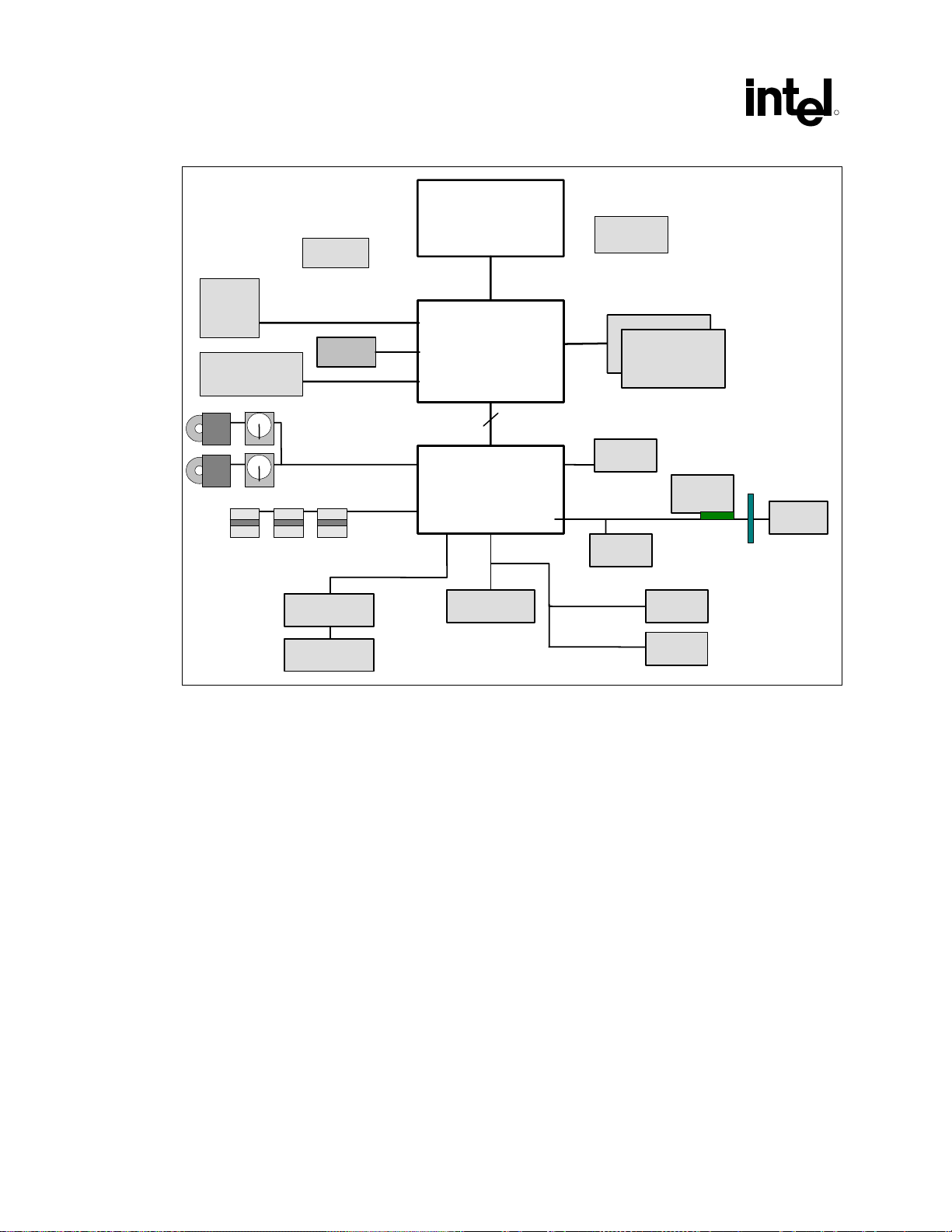
System Overview
Figure 1. Intel 852GM Chipset System Block Diagram
R
DVI
LFP
CK-408
DVOC
CRT
LVDS
ATA100 IDE (2)
USB2.0/1.1 (6)
AC'97 2.3
Audio Codec
Modem Codec
Processor
400 MHz BPSB
852GM
GMCH
732 Micro-
FCBGA
Hub
Interface 1.5
ICH 4-M
421 BGA
FWH
VR
200/266 MHz
LAN
PCI Bus
Cardbus
LPC I/F
DDR
SIO
KBC
Wireless
(802.11)
Mini-PCI
Moon 2
PCI Docking
2.2. Processor Interface
The 852GM GMCH supports a FSB frequency of 400 MHz (100-MHz HCLK respectively) using
scaleable FSB VCC.
All processors are design on the .13 micron process, maintain compatibility with IA-32 software, and are
designed for uni-processor based value systems
2.2.1. Mobile Intel Celeron Processor
The processor utilizes flip-chip pin grid array (FC-PGA2) package technology, which plugs into a 478pin surface mount, zero insertion force (ZIF) socket, referred to as the mPGA478B socket.
Processor features include:
• On-die, 256-kB second level cache
• Hyper pipelined technology
• 400-MHz Front Side Bus quad-pumped bus running off a 100-MHz system clock making 3.2
GB/sec data transfer rates possible
22 Intel
®
852GM Chipset Platform Design Guide
Page 23

R
• The execution trace cache is a first level cache that stores approximately 12-k decoded micro-
operations, which removes the decoder from the main execution path.
2.2.2. Mobile Intel Pentium 4 Processor-M
The processor utilizes flip-chip pin grid array (FC-PGA2) package technology, which plugs into a 478pin surface mount, zero insertion force (ZIF) socket, referred to as the mPGA478B socket.
Processor features include:
• On-die 512-kB second level cache
• Hyper pipelined technology
• 400-MHz Front Side Bus quad-pumped bus running off a 100-MHz system clock making 3.2
GB/sec data transfer rates possible
• Supports Streaming SIMD Extensions 2 (SSE2)
• Enhanced Intel
and frequency between two performance modes.
®
SpeedStep® technology which enables real-time dynamic switching of the voltage
System Overview
• 35-W thermal design power
2.2.3. Intel Celeron M Processor
The Intel Celeron M processor utilizes stocketable Micro Flip-Chip Pin Grid Array (Micro-FCPGA) and
surface mount Micro Flip-Chip Ball Grid Array(Micro-FCBGA) package technology. The MicroFCPGA package plugs into a 479-hole, surface-mount, zero insertion force (ZIF) socket, which is
referred to as the mPGA479M socket.
Processor features include:
• On-die primary 32-kB, instruction cache and 32-kbyte, write-back data cache
• On-die 512-kB second level cache
• Supports Streaming SIMD Extensions 2 (SSE2)
• Advanced Gunning Transceiver Logic (AGTL+) bus driver technology
• Supports host bus dynamic bus inversion (DINV)
• Dynamic power down of Data Bus buffers
• BPRI# control to Disable Address/Control buffers
• Package/Power
⎯ Micro-FCPGA and 479-ball Micro-FCBGA packages
⎯ VCC-CORE: Offered in 1.356 V standard voltage and 1.004 V ultra low voltage cores
⎯ VCCA (1.8 V)
⎯ VCCP (1.05 V)
The following list provides some of the key enhancement features on this processor:
• Supports Intel Architecture with Dynamic Execution
®
Intel
852GM Chipset Platform Design Guide 23
Page 24

System Overview
• AGTL+ bus driver technology with integrated GTL termination resistors (gated AGTL+ receivers
for reduced power)
• Supports 32 bit
• AGTL+ bus addressing (no support for 36-bit address extension)
• Supports uniprocessor systems
• 400-MHz, source-synchronous FSB
• 2X Address, 4X data
• High performance, low power core
• Advanced Branch Prediction and Data Prefetch Logic
• Advanced Power Management features
2.3. Intel 852GM Graphics Memory Controller Hub
2.3.1. Processor Front Side Bus Support
R
• AGTL+ bus driver technology (gated AGTL+ receivers for reduced power)
• Supports 32-bit AGTL+ bus addressing (no support for 36-bit address extension)
• Supports Uniprocessor (UP) systems
• 400 MT/s FSB support
• Supports in-order and dynamic deferred transactions
2.3.1.1. Integrated System Memory DRAM Controller
• PC1600/2100 system memory interface
• ECC not support
• Maximum of 1 GB of system memory by using 512-Mb technology devices
• Supports up to two double-sided SO-DIMMs (4 rows populated)
• Supports 64-Mb, 128-Mb, 256-Mb, and 512-Mb technologies for x8 and x16 width devices
• Supports 200-MHz and 266-MHz DDR devices
• 64-bit data interface
• Supports up to 16 simultaneous open pages
• Support for SO-DIMM Serial Presence Detect (SPD) scheme via SMBus interface
• S3 (STR) power management support via self refresh mode using CKE
2.3.2. Integrated Graphics Controller
• Graphics Core Frequency of 133 MHz
24 Intel
®
852GM Chipset Platform Design Guide
Page 25

System Overview
R
• 3D Graphics Engine
⎯ 3D Setup and Render Engine
⎯ High quality performance Texture Engine
• Analog Display Support
⎯ 350-MHz integrated 24-bit RAMDAC
⎯ Hardware color cursor support
⎯ Accompanying I2C and DDC channels provided through multiplexed interface
⎯ Hotplug and display support
⎯ Dual independent pipe for dual independent display
• Digital Video Out Port (DVO) support
⎯ Single channel DVO Port with 165-MHz dot clock support for a 12-bit interface
⎯ Compliant with DVI Specification 1.0
• Dedicated LFP (local flat panel) interface
⎯ Single or dual channel LVDS TFT panel support up to SXGA+ panel resolution with
frequency range from 25 MHz to 112 MHz per channel
⎯ SSC support of 0.5%, 1.0%, and 2.5% center and down spread with external SSC clock
⎯ Dual Display Twin (Single pipe LVDS+CRT) is not supported if SSC is enabled
⎯ Supports data format of 18 bpp
⎯ LCD panel power sequencing compliant with SPWG timing specification
⎯ Compliant with ANSI/TIA/EIA –644-1995 spec
⎯ Integrated PWM interface for LCD backlight inverter control
⎯ Compliant with CPIS Specification 1.5
⎯ Bi-linear Panel fitting
2.3.2.1. Packaging/Power
• 732-pin Micro-FCBGA (37.5 mm x 37.5 mm)
• VTTLF, VTTHF (1.05 V);
• VCC, VCCASM, VCCHL, VCCAHPLL, VCCAGPLL, VCCADPLLA, VCCADPLLB (1.2 V);
• VCCADAC, VCCDVO, VCCDLVDS, VCCALVDS, (1.5 V);
• VCCSM, VCCQSM, VCCTXLVDS (2.5 V);
• VCCGPIO (3.3 V)
2.3.3. I/O Controller Hub (ICH4-M)
The ICH4-M provides the I/O subsystem with access to the rest of the system:
• Upstream Accelerated Hub Architecture interface for access to the GMCH
• PCI 2.2 interface (6 PCI Request/Grant Pairs)
• Bus Master IDE controller (supports Ultra ATA 100/66/33)
• USB 1.1 and USB 2.0 Host Controllers
• High Speed Debug port via USB interface
• SMBus 2.0 Controller
®
Intel
852GM Chipset Platform Design Guide 25
Page 26

System Overview
• FWH Interface
• LPC Interface
• AC’97 2.3 Interface
• Alert-On-LAN*
• IRQ Controller
• IPAA security
2.3.3.1. Packaging/Power
• 421-pin, BGA package (31 mm x 31 mm)
VCC1_5 (1.5 V main logic voltage);
VCCSUS1_5 (1.5 V resume logic voltage);
VCCLAN1_5 (1.5 V LAN logic voltage);
VCC3_3 (3.3 V main I/O voltage);
VCCSUS3_3 (3.3 V resume I/O voltage);
VCCLAN3_3 (3.3 V LAN I/O voltage);
V5REF (5 V);
V5REF_SUS (5 V);
VCCRTC;
VCCHI (1.5 V);
VCCP (1.2-1.3 V)
R
26 Intel
®
852GM Chipset Platform Design Guide
Page 27

General Design Considerations
R
3. General Design Considerations
This section provides motherboard layout and routing guidelines. It does not discuss the functional
aspects of any bus, or the layout guidelines for an add-in device.
If the guidelines listed in this document are not followed, thorough signal integrity and timing
simulations should be ompleted for each design. Even when the guidelines are followed, Intel
recommends that critical signals be simulated to ensure proper signal integrity and flight time. Any
deviation from the guidelines should be simulated.
The trace impedance typically noted (i.e. 55 Ω ± 15%) is the “nominal” trace impedance for a 5-mil
wide external trace and a 4-mil wide internal trace. However, some stack-ups may lead to narrower or
wider traces on internal or external layers in order to meet the 55-Ω impedance target, that is, the
impedance of the trace when not subjected to the fields created by changing current in neighboring
traces. Note the trace impedance target assumes that the trace is not subjected to the EM fields created
by changing current in neighboring traces. It is important to consider the minimum and maximum
impedance of a trace based on the switching of neighboring traces when calculating flight times. Using
wider spaces between the traces can minimize this trace-to-trace coupling. In addition, these wider
spaces reduce settling time.
Coupling between two traces is a function of the coupled length, the distance separating the traces, the
signal edge rate, and the degree of mutual capacitance and inductance. In order to minimize the effects
of trace-to-trace coupling, the routing guidelines documented in this section should be followed. In
addition, all high speed, impedance controlled signals (e.g. FSB signals) should have continuous GND
referenced planes and cannot be routed over or under power/GND plane splits.
3.1. Nominal Board Stack-Up
The Intel 852GM chipset based platforms require a board stack-up yielding a target impedance of 55 Ω
± 15%. An example of an 8-layer board stack-up is shown in Figure 2. The left side of the figure
illustrates the starting dimensions of the metal and dielectric material thickness as well as drawn trace
width dimensions prior to lamination, conductor plating, and etching. After the motherboard materials
are laminated, conductors plated, and etched, somewhat different dimensions result. Dielectric materials
may become thinner, as under/over etching of conductors alters their trace width, and conductor plating
makes them thicker. It is important to note that for the purpose of extracting electrical models from
transmission line properties, the final dimensions of signals after lamination, plating, and etching should
be used.
The stack-up uses 1.2-mil (1 oz) copper on power planes to reduce I*R drops and 0.6-mil copper
thickness on the signal layers: primary side layer (L1), Layer 3 (L3), Layer 6 (L6), and secondary side
layer (L8).
To ensure impedance control of 55 Ω, the primary and secondary side layer micro-strip lines should
reference solid ground planes on Layer 2 and Layer 7, respectively.
®
Intel
852GM Chipset Platform Design Guide 27
Page 28
General Design Considerations
P
5
5
Figure 2. Recommended Board Stack-Up Dimensions
Dielectric Layer Layer Copper Trace Trace
R
Stackup
S
PREPREG
P 2 PLANE 1
CORE
S
PREPREG
CORE
P
PREPREG
S
CORE
P
PREPREG
S
Thickness No. Type
1 SIGNAL 1/2+plating
=> 5.0
=> 5.0
3SIGNAL 1
=> 12.0
4PLANE1
=> 10.0
5PLANE1
=> 12.0
6SIGNAL 1
=> 5.0
7PLANE1
=> 5.0
8 SIGNAL 1/2+plating
Weight Width Impedance
(oz)(mils)
(mils) (ohms)
5.0 55
4.0 55
4.0 5
5.0 5
Internal signal traces on Layer 3 and Layer 6 are unbalanced strip-lines. To meet the nominal 55-Ω
characteristic impedance for these traces, they reference a solid ground plane on Layer 2 and Layer 7.
Since the coupling to Layer 4 and Layer 5 is still significant, (especially true when thinner stack-ups use
balanced strip-lines on internal layers) these layers are converted to ground floods in the areas of the
motherboard where the speed critical interfaces like the FSB or DDR system memory are routed. In the
remaining sections of the motherboard layout the Layer 4 and Layer 5 layers are used for power
delivery.
The secondary side layer (L8) is also used for power delivery in many cases, since it benefits from the
thick copper plating of the external layer plating as well as referencing the close Layer 7 ground plane.
The benefit of such a stack-up is low inductance power delivery.
28 Intel
®
852GM Chipset Platform Design Guide
Page 29

R
3.2. Alternate Stack Ups
OEMs may choose to use different stack-ups (number of layers, thickness, trace width, etc.) from the
one example outlined in Figure 2. However, the following key elements should be observed:
1. Final post lamination, post etching, and post plating dimensions should be used for electrical
model extractions.
2. Power plane layers should be 1 oz thick and signal layers should be ½ oz thick. External layers
become 1 – 1.5 oz (1.2 – 2 mils) thick after plating.
3. All high-speed signals should reference solid ground planes through the length of their routing
and should not cross plane splits. To guarantee this, both planes surrounding strip-lines should be
GND.
4. Intel recommends that high-speed signal routing be done on internal, strip-line layers.
5. For high-speed signals transitioning between layers next to the component, the signal pins should
be accounted for by the GND stitching vias that would stitch all the GND plane layers in that area
of the motherboard. Due to the arrangement of the Processor and 852GM GMCH pin-maps, GND
vias placed near all GND lands will also be very close to high-speed signals that may be
transitioning to an internal layer. Thus, no additional ground stitching vias (besides the GND pin
vias) are required in the immediate vicinity of the Processor and 852GM GMCH packages to
accompany the signal transitions from the component side into an internal layer.
6. High-speed routing on external layers should be minimized in order to avoid EMI. Routing on
external layers also introduces different delays compared to internal layers. This makes it
extremely difficult to do length matching if some routing is done on both internal and external
layers.
7. If Intel’s recommended stackup guidelines are not implemented, then the OEM is liable for all
aspects of their board design and simulations should be performed based on OEM stackup (i.e.
understanding impacts of SI and power distribution).
General Design Considerations
®
Intel
852GM Chipset Platform Design Guide 29
Page 30

General Design Considerations
R
This page intentionally left blank.
30 Intel
®
852GM Chipset Platform Design Guide
Page 31

Mobile Intel Pentium 4 Processor–M and Mobile Intel Celeron Processor FSB Design Guidelines
R
4. Mobile Intel Pentium 4 Processor–M
and Mobile Intel Celeron Processor
FSB Design Guidelines
The following layout guidelines support designs using the Mobile Intel Pentium 4 Processor–M / Mobile
Intel Celeron Processor and the Intel 852GM chipset. Due to on-die Rtt resistors on both the processor
and the chipset, additional resistors do not need to be placed on the motherboard for most FSB signals.
The exception to these are the RESET# and BPM[5:0]# signals that require a 51.1-Ω pull-up, and the
BR0 signal that requires 220-Ω + 5% pull-up to Vtt on the processor end of the transmission line.
4.1. Processor Front Side Bus (FSB) Routing Guidelines
Table 1 summarizes the layout recommendations for the Mobile Intel Pentium 4 Processor–M and
expands on specific design issues and their recommendations.
Table 1. Front Side Bus Routing Summary for the Processor
Parameter Processor Routing Guidelines
Line to line
spacing
Data Line lengths
(agent to agent
spacing)
DSTBn/p[3:0]# • A data strobe and its complement should be routed within ± 0.025 inches of the same pad-to-
Address line
lengths (agent to
agent spacing)
Greater than or equal to 2:1 edge-to-edge spacing versus trace width.
See Figure 3 for an illustration of this recommendation.
0.5 inches–5.5 inches from pin-to-pin.
• Data signals of the same source synchronous group should be routed to the same pad-to-pad
length within ± 0.100 inches of the associated strobes.
• The pad is defined as the attach point of the silicon die to the package substrate.
• Length must be added to the system board to compensate for package length differences.
• Signals in the same source synchronous group should be routed on the same layer and
referenced to Vss with 2:1 spacing.
pad length.
• The pad is defined as the attach point of the silicon die to the package substrate.
• Length must be added to the system board to compensate for package length differences.
• DSTBn/p# should be routed on the same layer as their associated data group and referenced
to Vss.
0.5 inches – 6.5 inches from pin-to-pin.
• Address signals of the same source synchronous group should be routed to the same Pad-toPad length within± 0.200 inches of the associated strobes.
• The pad is defined as the attach point of the silicon die to the package substrate.
• Length must be added to the system board to compensate for package length differences.
• A layer transition may occur if the reference plane remains the same (Vss) and the layers are
of the same configuration (all stripline or all microstrip).
®
Intel
852GM Chipset Platform Design Guide 31
Page 32

Mobile Intel Pentium 4 Processor–M and Mobile Intel Celeron Processor FSB Design Guidelines
Parameter Processor Routing Guidelines
ADSTBn/p[1:0]# • An address strobe and its complement should be routed within ± 0.200 of the same Pad-to-
Common Clock
line lengths
Topology Stripline
Routing priorities • All associated signals and strobes should be routed on same layer for entire length of bus.
Clock keepout
zones
Trace Impedance 55 ohms ± 15%
Source
Synchronous
routing restrictions
Pad length.
• The pad is defined as the attach point of the silicon die to the package substrate.
• Length must be added to the system board to compensate for package length differences.
• A layer transition may occur if the reference plane remains the same (Vss) and the layers are
of the same configuration (all stripline or all microstrip).
0.5 inches – 6.5 inches
• All signals should be referenced to Vss. Ideally, layer changes should not occur for any
signals.
• If a layer change must occur, reference plane must be Vss and the layers must all be of the
same configuration (all stripline or all microstrip for example).
A spacing requirement of 16-20 mils should be maintained around all clocks.
• There are no length-matching routing restrictions between (or within) either the sourcesynchronous data or address groups.
• As long as the strobe and associated line length routing guidelines are met for each group,
there is no need to length-match between the groups. For example, one data group may be
routed to the minimum allowable length while another data group could be routed to the
maximum allowable length.
• Simulations have verified that the FSB will still function correctly even under this extreme
condition.
R
Refer to the Intel® 852GM Chipset GMCH Datasheet for GMCH package dimensions and refer to the
Mobile Intel
®
Pentium® 4 Processor–M Datasheet for processor package dimensions.
Figure 3. Cross-Sectional View of 2:1 Ratio
trace
NOTE: This is the edge-to-edge trace spacing versus width.
A trace spacing to width ratio of 2 to 1 ensures a low crosstalk coefficient (based on geometries defined
in 8 layer reference stackup). All the effects of crosstalk are difficult to simulate. The timing and layout
guidelines for the processor have been created with the assumption of 2 to 1 trace spacing to width ratio.
A smaller ratio would have an unpredictable impact due to crosstalk.
Reference Plane
2x
trace
x
32 Intel
®
852GM Chipset Platform Design Guide
Page 33

Mobile Intel Pentium 4 Processor–M and Mobile Intel Celeron Processor FSB Design Guidelines
R
4.1.1. Return Path Evaluation
The return path is the route current takes to return to its source. It may take a path through ground
planes, power planes, other signals, integrated circuits, vias, VRMs, etc. Think of the return path as
following a path of least impedance back to the original source. Discontinuities in the return path often
have signal integrity and timing effects that are similar to the discontinuities in the signal conductor.
Therefore, the return paths need to be given similar considerations. A simple way to evaluate return path
parasitic inductance is to draw a loop that traces the current from the driver through the signal conductor
to the receiver, and then back through the ground/power plane to the driver again. The smaller the area
of the loop, the lower the parasitic inductance will be.
The following set of return path rules apply:
• Always trace out the return current path and provide as much care to the return path as the path of
the signal conductor.
• Decoupling capacitors do not adequately compensate for a plane split.
• Do not allow splits in the reference planes in the path of the return current.
• Do not allow routing of signals on the reference planes near Front Side Bus signals.
• Maintain Vss as a reference plane for all Front Side Bus signals.
• Do not route over via anti-pads or socket anti-pads.
4.2. Processor Configuration
This section provides more details for routing Mobile Intel Pentium 4 Processor–M- based systems. This
information is preliminary and subject to change. Both recommendations and considerations are
presented.
For proper operation of the Mobile Pentium 4 Processor-M and the Intel 852GM chipset, it is necessary
that the system designer meet the timing and voltage specifications of each component. The following
recommendations are Intel’s best guidelines based on extensive simulation and experimentation that
make assumptions, which may be different than an OEM's system design. The most accurate way to
understand the signal integrity and timing of the Front Side Bus in your platform is by performing a
comprehensive simulation analysis. It is conceivable that adjustments to trace impedance, line length,
termination impedance, board stackup and other parameters can improve system performance.
®
Refer to the Mobile Intel
types and definitions.
Pentium® 4 Processor–M Datasheet for a Front Side Bus signal list, signal
4.3. General Topology and Layout Design Guidelines
The following topology and layout guidelines are based on routing recommendations implemented on
Intel Customer reference board. The guidelines are derived from empirical testing with Intel 852GM
chipset package models. Below are the design recommendations for the data, address, strobes, and
common clock signals. For the following discussion, the pad is defined as the attach point of the silicon
die to the package substrate.
®
Intel
852GM Chipset Platform Design Guide 33
Page 34

Mobile Intel Pentium 4 Processor–M and Mobile Intel Celeron Processor FSB Design Guidelines
−+−
4.3.1. Source Synchronous (SS) Signal Group
Source synchronous groups and associated strobes should be routed on the same layer for the entire
length of the bus. This results in a significant reduction of the flight time skew since the dielectric
thickness, line width, and velocity of the signals will be uniform across a single layer of the stackup.
There is no guarantee of a relationship of dielectric thickness, line width, and velocity between layers.
Figure 4. Processor Topology
R
Processor
Pad
Length L1
Package trace
Motherboard PCB trace
GMCH
Pad
4.3.1.1. Source Synchronous Data Group
Data signals of the same source synchronous group should be routed to the same pad-to-pad length
within ± 0.100 of the associated strobes (within the min & max of both strobe). As a result, additional
trace will be added to some data nets on the system board in order for all trace lengths within the same
data group to be the same length (± 0.100 inches) from the pad of the processor to the associated pad
of the chipset.
A data strobe and its complement should be routed to a length equal to their corresponding data group's
mean pad-to-pad length ± 0.025 inches.
Equation 1. Calculation to Determine Package Delta Addition to Motherboard Length for UP
Systems
=
Refer to the Intel
Mobile Intel
®
Pentium® 4 Processor–M Datasheet for package dimensions.
®
852GM Chipset GMCH Datasheet for GMCH package dimensions and refer to the
)cs_pkglen(cs_pkglen)cpu_pkglenn(cpu_pkgledelta
strobenet*strobenetnet,strobe
Note: * Strobe package length is the average of the strobe pair.
34 Intel
®
852GM Chipset Platform Design Guide
Page 35

Mobile Intel Pentium 4 Processor–M and Mobile Intel Celeron Processor FSB Design Guidelines
R
Table 2. Processor Front Side Bus Data Signal Routing Guidelines
Signal Names Total Trace Length
CPU GMCH
DBI[3:0]# DINV[3:0]# Strip-line 0.5 5.5 55 ± 15% 4 & 12
D[63:0]# HD[63:0]# Strip-line 0.5 5.5 55 ±15% 4 & 12
DSTBN[3:0]# HDSTBN[3:0]# Strip-line 0.5 5.5 55 ± 15% 4 & 12
DSTBP[3:0]# HDSTBP[3:0]# Strip-line 0.5 5.5 55 ±15% 4 & 12
NOTES:
1. The Data signals within each group must be routed to within ± 0.100 inches of its associated “reference” strobe
(within the min & max of both strobe).
2. The complement strobe must be routed to within ± 0.025 inches of the associate “reference” strobe.
3. All traces within each signal group must be routed on the same layer (required).
4. Intel recommends that length of the strobes be centered to the average length of associated data or address
traces to maximize setup/hold time margins.
Transmission
Line Type
Min
(inches)
4.3.1.2. Source Synchronous Address Group
Address signals follow the same rules as data signals except they should be routed to the same pad-topad length within ± 0.200 inches of the associated strobes. Address signals may change layers if the
reference plane remains Vss.
An address strobe should be routed to a length equal to their corresponding signal group's mean pad-to-
pad length ± 0.025 inches.
Max
(inches)
Nominal
Impedance
(Ω)
Width & Spacing
(mils)
1:3
Table 3. Processor Front Side Bus Address Signal Routing Guidelines
Signal Names Total Trace Length
CPU GMCH
A[31:3]# HA[31:3]# Strip-line 0.5 6.5 55 ± 15% 4 & 8
REQ[4:0]# HREQ[4:0]# Strip-line 0.5 6.5 55 ± 15% 4 & 8
ADSTB[1:0]# HADSTB[1:0]# Strip-line 0.5 6.5 55 ± 15% 4 & 8
NOTES:
1. The Address signals within each group must be routed to within ± 0.200 of its associated strobe.
2. All traces within each signal group must be routed on the same layer (required).
3. It is recommended that length of the strobes be centered to the average length of associated data or address
traces to maximize setup/hold time margins.
Transmission
Line Type
Min
(inches)
Max
(inches)
Nominal
Impedance
(Ω)
Width & Spacing
(mils)
®
Intel
852GM Chipset Platform Design Guide 35
Page 36

Mobile Intel Pentium 4 Processor–M and Mobile Intel Celeron Processor FSB Design Guidelines
Figure 5. SS Topology for Address and Data
R
Processor Chip Set
Vtt
Pad
Pin
Pin
L1
4.3.2. FSB Data and Address Routing Example
Figure 6, Figure 7, Figure 8, and Figure 9 provide examples of a board routing for the Data signal group.
The majority of the Data signal route is on an internal layer; both external layers can be used for parallel
termination R-pack placement.
Figure 6. FSB Host Data Routing Example Layer 3
Vtt
Pad
Layer 3
FSB Data signals
36 Intel
®
852GM Chipset Platform Design Guide
Page 37

Mobile Intel Pentium 4 Processor–M and Mobile Intel Celeron Processor FSB Design Guidelines
R
Figure 7. FSB Host Address Routing Example Layer 3
Layer 3
FSB Address signals
Figure 8. FSB Host Data Routing Example Layer 6
Layer 6
FSB Data signals
®
Intel
852GM Chipset Platform Design Guide 37
Page 38

Mobile Intel Pentium 4 Processor–M and Mobile Intel Celeron Processor FSB Design Guidelines
Figure 9. FSB Host Address Routing Example Layer 6
Layer 6
FSB Address signals
R
38 Intel
®
852GM Chipset Platform Design Guide
Page 39

Mobile Intel Pentium 4 Processor–M and Mobile Intel Celeron Processor FSB Design Guidelines
R
4.3.3. Common Clock (CC) AGTL+ Signal Group
Common clock signals should be routed to a minimum pin-to-pin motherboard length of 0.5 inches and
a maximum motherboard length of 6.5 inches.
Table 4. Processor Front Side Bus Control Signal Routing Guidelines
Signal Names
Topology
CPU GMCH
RESET# CPURST# Stripline 6.5 0.5 55 ± 15% 4 & 8
BR0# BREQ0# Stripline 6.5 0.5 55 ± 15% 4 & 8
BNR# BNR# Stripline 6.5 0.5 55 ± 15% 4 & 8
REQ[4:0]# HREQ[4:0]# Stripline 6.5 0.5 55 ± 15% 4 & 8
BPRI# BPRI# Stripline 6.5 0.5 55 ± 15% 4 & 8
DEFER# DEFER# Stripline 6.5 0.5 55 ± 15% 4 & 8
LOCK# HLOCK# Stripline 6.5 0.5 55 ± 15% 4 & 8
TRDY# HTRDY# Stripline 6.5 0.5 55 ± 15% 4 & 8
DRDY# DRDY# Stripline 6.5 0.5 55 ± 15% 4 & 8
ADS# ADS# Stripline 6.5 0.5 55 ± 15% 4 & 8
DBSY# DBSY# Stripline 6.5 0.5 55 ± 15% 4 & 8
HIT# HIT# Stripline 6.5 0.5 55 ± 15% 4 & 8
HITM# HITM# Stripline 6.5 0.5 55 ± 15% 4 & 8
RS[2:0]# RS[2:0]# Stripline 6.5 0.5 55 ± 15% 4 & 8
NOTES:
1. Trace width of 4 mils and trace spacing of 8 mils within signal groups. Entire trace for each signal routed on one
layer (recommended)
2. RESET# and BR0# are common clock AGTL+ signals without ODT (On die termination). These signals require
an external Rtt. The Rtt should be placed near CPU: L2<= 0.5 inches. Rtt = 51.1 ±1%.
Routing Trace Length
(Pin-to-Pin)
Max
(inches)
Min
(inches)
Nominal Impedance
(ohms)
Width & Spacing
(mils)
4.3.4. Asynchronous AGTL+ Signals
All signals must meet the AC and DC specifications as documented in the Mobile Intel® Pentium® 4
Processor–M Datasheet.
4.3.4.1. Topology 1A: Open Drain (OD) Signals Driven by the Processor – IERR#
and FERR#
The Topology 1A OD signals IERR# and FERR# should adhere to the following routing and layout
recommendations. Table 5 lists the recommended routing requirements for the IERR# and FERR#
signals of the Mobile Intel Pentium 4 Processor–M. The routing guidelines allow the signal to be routed
®
Intel
852GM Chipset Platform Design Guide 39
Page 40

Mobile Intel Pentium 4 Processor–M and Mobile Intel Celeron Processor FSB Design Guidelines
as either micro-strip or strip-lines using 55 Ω ± 15% characteristic trace impedance. The pull-up voltage
for termination resistor Rtt is VCCP.
Due to the dependencies on system design implementation, IERR# can be implemented in a number of
ways to meet design goals. IERR# can be routed as a test point or to any optional system receiver. It is
recommended that the FERR# signal of the Intel Mobile Intel Pentium 4 Processor–M be routed to the
FERR# signal of the Intel ICH4-M.
Figure 10. Routing Illustration for Topology 1A
CPU
System
Receiver
L2
VCCP
Rtt
R
L1
L3
Table 5. Layout Recommendations for Topology 1A
L1 L2 L3 Rtt Transmission Line Type
0.5” – 12.0” 0” – 3.0” 0” – 3.0” 56 Ω ± 5% Micro-strip
0.5” – 12.0” 0” – 3.0” 0” – 3.0” 56 Ω ± 5% Strip-line
4.3.4.2. Topology 1B: Open Drain (OD) Signals Driven by the Processor –
THERMTRIP#
The Topology 1B OD signal THERMTRIP# should adhere to the following routing and layout
recommendations. Table 6 lists the recommended routing requirements for the THERMTRIP# signals of
the Mobile Intel Pentium 4 Processor–M. The routing guidelines allow the signal to be routed as either
micro-strip or strip-lines using 55 Ω ± 15% characteristic trace impedance. The pull-up voltage for
termination resistor Rtt is VCCP.
THERMTRIP# can be implemented in a number of ways to meet design goals. It can be routed to the
ICH4-M or any optional system receiver. Intel recommneds that the THERMTRIP# signal of the Mobile
Intel Pentium 4 Processor–M be routed to the THRMTRIP# signal of the ICH4-M. The ICH4-M’s
THRMTRIP# signal is a new signal to the I/O controller hub architecture that allows the ICH4-M to
quickly put the whole system into an S5 state whenever the catastrophic thermal trip point has been
reached.
40 Intel
®
852GM Chipset Platform Design Guide
Page 41

Mobile Intel Pentium 4 Processor–M and Mobile Intel Celeron Processor FSB Design Guidelines
R
Figure 11. Routing Illustration for Topology 1B
CPU
ICH4-M
(or sys. receiver)
VCCP
Rtt
L2
L1
L3
Table 6. Layout Recommendations for Topology 1B
L1 L2 L3 Rtt Transmission Line Type
0.5” – 12.0” 0” – 3.0” 0” – 3.0” 56 Ω ± 5% Micro-strip
0.5” – 12.0” 0” – 3.0” 0” – 3.0” 56 Ω ± 5% Strip-line
4.3.4.3. Topology 1C: Open Drain (OD) Signals Driven by the Processor –
PROCHOT#
The Topology 1C OD signal PROCHOT#, should adhere to the following routing and layout
recommendations. Table 7 lists the recommended routing requirements for the PROCHOT# signal. The
routing guidelines allow the signal to be routed as either a micro-strip or strip-line using 55 Ω ± 15%
characteristic trace impedance. Figure 12 shows the recommended implementation for providing voltage
translation between the processor’s PROCHOT# signal and a system receiver that utilizes a 3.3-V
interface voltage (shown as VCCP).
Series resistor Rs is a component of the voltage translation logic and serves as a driver isolation resistor.
Rs is shown separated by distance L3 from the first bipolar junction transistor (BJT), Q1, to emphasize
the placement of Rs with respect to Q1. The placement of Rs a distance L3 before the Q1 BJT is a
specific implementation of the generalized voltage translator circuit shown in Figure 17. Rs should be
placed at the beginning of the T-split from the PROCHOT# signal. The pull-up voltage for termination
resistor Rtt is VCCP.
Intel recommends that PROCHOT# be routed using the voltage translation logic shown in Figure 12.
®
Intel
852GM Chipset Platform Design Guide 41
Page 42

Mobile Intel Pentium 4 Processor–M and Mobile Intel Celeron Processor FSB Design Guidelines
Figure 12. Routing Illustration for Topology 1C
R
CPU
VCCP
Rtt
L2
L1
L3
Rs
Table 7. Layout Recommendations for Topology 1C
L1 L2 L3 L4 Rs R1 R2 Rtt Transmission
0.5 –
12.0”
0.5 –
12.0”
0 -
3.0”
0 -
3.0”
0 –
3.0”
0 –
3.0”
0.5 –
12.0”
0.5 –
12.0”
330 Ω ± 5% 1.3 kΩ ± 5 % 330 Ω ± 5% 56 Ω ± 5% Micro-strip
330 Ω ± 5% 1.3 kΩ ± 5% 330 Ω ± 5% 56 Ω ± 5% Strip-line
Q1
3.3
R1
390
Q2
3.3
R2
390
L4
(System receiver)
V_IO_RCVR
Line Type
4.3.4.4. Topology 2A: Open Drain (OD) Signals Driven by ICH4-M – PWRGOOD
The Topology 2A OD signal PWRGOOD should adhere to the following routing and layout
recommendations.
Table 8 lists the recommended routing requirements for the PWRGOOD signal of the Mobile Intel
Pentium 4 Processor–M. The routing guidelines allow the signal to be routed as either micro-strip or
strip-lines using 55 Ω ± 15% characteristic trace impedance. The pull-up voltage for termination resistor
Rtt is VCCP. Note that the Intel ICH4-M’s CPUPWRGD signal should be routed point-to-point to the
Mobile Intel Pentium 4 Processor–M’s PWRGOOD signal. The routing from the Mobile Intel Pentium 4
Processor–M’s PWRGOOD pin should fork out to both to the termination resistor, Rtt, and the ICH4-M.
Segments L1 and L2 from Figure 13 should not T-split from a trace from the Mobile Intel Pentium 4
Processor–M pin.
42 Intel
®
852GM Chipset Platform Design Guide
Page 43

Mobile Intel Pentium 4 Processor–M and Mobile Intel Celeron Processor FSB Design Guidelines
R
Figure 13. Routing Illustration for Topology 2A
VCCP
Rtt
L2
CPU
L1
Table 8. Layout Recommendations for Topology 2A
L1
0.5” – 12.0” 0” – 3.0” 300 Ω ± 5% Micro-strip
0.5” – 12.0” 0” – 3.0” 300 Ω ± 5% Strip-line
L2 Rtt Transmission Line Type
4.3.4.5. Topology 2B: CMOS Signals Driven by ICH4-M – DPSLP#
The Topology 2B CMOS DPSLP# signal should adhere to the following routing and layout
recommendations illustrated in Figure 14. As listed in Table 9, the L1 and L2 segments of the DPSLP#
signal topology can be routed as either micro-strip or strip-lines using 55 Ω ± 15% characteristic trace
impedance. Note that the Intel ICH4-M’s DPSLP# signal should be routed point-to-point with the daisy
chain topology shown. The routing of DPSLP# at the CPU should fork out to both the ICH4-M and the
GMCH. Segments L1 and L2 from Figure 14 should not T-split from a trace from the Mobile Intel
Pentium 4 Processor–M pin.
ICH4-M
Figure 14. Routing Illustration for Topology 2B
GMCH
L2
Table 9. Layout Recommendations for Topology 2B
L1 L2 Transmission Line Type
0.5” – 12.0” 0.5” – 6.5” Micro-strip
0.5” – 12.0” 0.5” – 6.5” Strip-line
CPU
L1
ICH4-M
®
Intel
852GM Chipset Platform Design Guide 43
Page 44
Mobile Intel Pentium 4 Processor–M and Mobile Intel Celeron Processor FSB Design Guidelines
4.3.4.6. Topology 2C: CMOS Signals Driven by ICH4-M – A20M#, IGNNE#,
LINT0/INTR, LINT1/NMI, SLP#, SMI#, and STPCLK#
The Topology 2C CMOS A20M#, IGNNE#, LINT0/INTR, LINT1/NMI, SLP#, SMI#, and STPCLK#
signals should implement a point-to-point connection between the ICH4-M and the Mobile Intel
Pentium 4 Processor–M. The routing guidelines allow both signals to be routed as either micro-strip or
strip-lines using 55 Ω ± 15% characteristic trace impedance. No additional motherboard components are
necessary for this topology.
Figure 15. Routing Illustration for Topology 2C
R
CPU
L1
ICH4-M
Table 10. Layout Recommendations for Topology 2C
L1 Transmission Line Type
0.5” – 12.0” Micro-strip
0.5” – 12.0” Strip-line
4.3.4.7. Topology 3: CMOS Signals Driven by ICH4-M to CPU and FWH – INIT#
The signal INIT# should adhere to the following routing and layout recommendations.
Table 11 lists the recommended routing requirements for the INIT# signal of the ICH4-M. The routing
guidelines allow both signals to be routed as either micro-strip or strip-lines using 55 Ω ± 15%
characteristic trace impedance.
Figure 16 shows the recommended implementation for providing voltage translation between the ICH4M’s INIT# voltage signaling level and any firmware hub (FWH) that utilizes a 3.3-V interface voltage
(shown as a supply 3.3V). For convenience, the entire topology and required transistors and resistors for
the voltage translator is shown in Figure 16.
Series resistor Rs is a component of the voltage translator logic circuit and serves as a driver isolation
resistor. Rs is shown separated by distance L3 from the first bipolar junction transistor (BJT), Q1, to
emphasize the placement of Rs with respect to Q1. The routing recommendations of transmission line
L3 in Figure 16 is listed in
Table 11 and Rs should be placed at the beginning of the T-split of the trace from the ICH4-M’s INIT#
pin.
44 Intel
®
852GM Chipset Platform Design Guide
Page 45

Mobile Intel Pentium 4 Processor–M and Mobile Intel Celeron Processor FSB Design Guidelines
r
r
R
Figure 16. Routing Illustration for Topology 3
CPU ICH4-M
L1
L2
Rs
L3
Q1
Table 11. Layout Recommendations for Topology 3
L1 + L2 L3 L4 Rs R1 R2 Transmission Line
0.5” – 12.0” 0” – 3.0” 0.5” – 6.0” 300 Ω ± 5% 2kΩ ± 5% 300 Ω ± 5% Micro-strip
0.5” – 12.0” 0” – 3.0” 0.5” – 6.0” 300 Ω ± 5% 2kΩ ± 5% 300 Ω ± 5% Strip-line
Figure 17. Voltage Translation Circuit for 3.3-V Receivers
3.3V
R1
3904
Q2
3.3V
R2
3904
FWH
V_IO_FW H
L4
Type
From Drive
4.4. ITP Debug Port
Please refer to the ITP700 Debug Port Design Guide, which can be found on
http://developer.intel.com/design/Xeon/guides/249679.htm
Note: This change is effective for all future processors and includes information on both ITP700 and ITP700
Flex.
330 ohm
+/- 5%
Rs
1.3K ohm
+/- 5%
Q1
3.3V
R1
3904
330 ohm
+/- 5%
Q2
.
3.3V
R2
To Receive
3904
®
Intel
852GM Chipset Platform Design Guide 45
Page 46

Mobile Intel Pentium 4 Processor–M and Mobile Intel Celeron Processor FSB Design Guidelines
4.4.1. Logic Analyzer Interface (LAI)
Intel is working with two logic analyzer vendors to provide logic analyzer interfaces (LAIs) for use in
debugging the Mobile Intel Pentium 4 Processor–M based system. Tektronix* and Agilent* should be
contacted to get specific information about their logic analyzer interfaces. The following information is
general in nature. Specific information must be obtained from the logic analyzer vendor.
Due to the complexity of the Mobile Intel Pentium 4 Processor–M based system, the LAI is critical in
providing the ability to probe and capture Front Side Bus signals. There are two sets of considerations to
keep in mind when designing a Mobile Intel Pentium 4 Processor–M that can make use of an LAI:
mechanical and electrical.
4.4.1.1. Mechanical Considerations
The LAI is installed between the processor socket and the Mobile Intel Pentium 4 Processor–M. The
LAI pins plug into the socket, while the Mobile Intel Pentium 4 Processor–M plugs into a socket on the
LAI. Cabling that is part of the LAI egresses the system to allow an electrical connection between the
Mobile Intel Pentium 4 Processor–M and a logic analyzer. The maximum volume occupied by the LAI,
known as the keepout volume, as well as the cable egress restrictions, should be obtained from the logic
analyzer vendor. System designers must make sure that the keepout volume remains unobstructed inside
the system. Note that it is possible that the keepout volume reserved for the LAI may include space
normally occupied by the Mobile Intel Pentium 4 Processor–M heat sink. If this is the case, the logic
analyzer vendor will provide a cooling solution as part of the LAI.
R
4.4.1.2. Electrical Considerations
The LAI will also affect the electrical performance of the Front Side Bus; therefore, it is critical to
obtain electrical load models from each of the logic analyzers in order to run system level simulations to
prove that their tool will work in the system. Contact the logic analyzer vendor for electrical
specifications and load models for the LAI solution they provide.
4.5. Mobile Intel Pentium 4 Processor–M and Intel 852GM
Chipset FSB Signal Package Lengths
Table 12 lists the preliminary package trace lengths of the Mobile Intel Pentium 4 Processor–M and the
Intel 852GM GMCH for the source synchronous data and address signals. Refer to Section 4.3.1 for
further details. The Mobile Intel Pentium 4 Processor–M and Intel 852GM GMCH package traces are
routed as micro-strip lines with a nominal characteristic impedance of 55 Ω ± 15%.
Table 12. Mobile Intel Pentium 4 Processor-M and Intel 852GM Chipset Package Lengths
Processor lengths GMCH Lengths
Signal Processor
ADSTB[0]# L5 0.210 HADSTB[0]# T26 419
A[3]# K2 0.368 HA[3]# P23 468
A[4]# K4 0.265 HA[4]# T25 353
Ball
Length
(inches)
Address Group 0
Signal GMCH ball Length
(mils)
46 Intel
®
852GM Chipset Platform Design Guide
Page 47

Mobile Intel Pentium 4 Processor–M and Mobile Intel Celeron Processor FSB Design Guidelines
R
Processor lengths GMCH Lengths
A[5]# L6 0.155 HA[5]# T28 551
A[6]# K1 0.415 HA[6]# R27 523
A[7]# L3 0.304 HA[7]# U23 274
A[8]# M6 0.144 HA[8]# U24 333
A[9]# L2 0.372 HA[9]# R24 327
A[10]# M3 0.327 HA[10]# U28 560
A[11]# M4 0.246 HA[11]# V28 566
A[12]# N1 0.394 HA[12]# U27 522
A[13]# M1 0.408 HA[13]# T27 501
A[14]# N2 0.349 HA[14]# V27 562
A[15]# N4 0.241 HA[15]# U25 375
A[16]# N5 0.198 HA[16]# V26 491
REQ[0]# J1 0.427 HREQ[0]# R28 569
REQ[1]# K5 0.207 HREQ[1]# P25 378
REQ[2]# J4 0.270 HREQ[2]# R23 247
REQ[3]# J3 0.337 HREQ[3]# R25 383
REQ[4]# H3 0.356 HREQ[4]# T23 276
Address Group 1
ADSTB[1]# R5 0.214 HADSTB[1]# AA26 504
A[17]# T1 0.470 HA[17]# Y24 457
A[18]# R2 0.404 HA[18]# V25 389
A[19]# P3 0.303 HA[19]# V23 284
A[20]# P4 0.246 HA[20]# W25 414
A[21]# R3 0.334 HA[21]# Y25 429
A[22]# T2 0.388 HA[22]# AA27 545
A[23]# U1 0.458 HA[23]# W24 382
A[24]# P6 0.156 HA[24]# W23 353
A[25]# U3 0.379 HA[25]# W27 536
A[26]# T4 0.281 HA[26]# Y27 556
A[27]# V2 0.417 HA[27]# AA28 631
A[28]# R6 0.166 HA[28]# W28 579
A[29]# W1 0.493 HA[29]# AB27 558
A[30]# T5 0.217 HA[30]# Y26 484
A[31]# U4 0.285 HA[31]# AB28 617
Data Group 0
DSTBN[0]# E22 0.338 HDSTBN[0]# J28 763
DSTBP[0]# F21 0.326 HDSTBP[0]# K27 662
®
Intel
852GM Chipset Platform Design Guide 47
Page 48

Mobile Intel Pentium 4 Processor–M and Mobile Intel Celeron Processor FSB Design Guidelines
Processor lengths GMCH Lengths
D[0]# B21 0.414 HD[0]# K22 329
D[1]# B22 0.475 HD[1]# H27 620
D[2]# A23 0.538 HD[2]# K25 438
D[3]# A25 0.608 HD[3]# L24 387
D[4]# C21 0.386 HD[4]# J27 600
D[5]# D22 0.386 HD[5]# G28 693
D[6]# B24 0.535 HD[6]# L27 518
D[7]# C23 0.464 HD[7]# L23 329
D[8]# C24 0.515 HD[8]# L25 458
D[9]# B25 0.590 HD[9]# J24 438
D[10]# G22 0.274 HD[10]# H25 504
D[11]# H21 0.203 HD[11]# K23 319
D[12]# C26 0.589 HD[12]# G27 620
D[13]# D23 0.462 HD[13]# K26 494
D[14]# J21 0.183 HD[14]# J23 393
D[15]# D25 0.550 HD[15]# H26 554
DBI[0]# E21 0.309 DINV[0]# J25 514
Data Group 1
DSTBN[1]# K22 0.301 HDSTBN[1]# C27 788
DSTBP[1]# J23 0.306 HDSTBP[1]# D26 736
D[16]# H22 0.272 HD[16]# F25 593
D[17]# E24 0.480 HD[17]# F26 634
D[18]# G23 0.358 HD[18]# B27 834
D[19]# F23 0.418 HD[19]# H23 412
D[20]# F24 0.443 HD[20]# E27 714
D[21]# E25 0.508 HD[21]# G25 522
D[22]# F26 0.513 HD[22]# F28 731
D[23]# D26 0.597 HD[23]# D27 766
D[24]# L21 0.176 HD[24]# G24 493
D[25]# G26 0.524 HD[25]# C28 837
D[26]# H24 0.412 HD[26]# B26 815
D[27]# M21 0.171 HD[27]# G22 453
D[28]# L22 0.245 HD[28]# C26 768
D[29]# J24 0.401 HD[29]# E26 691
D[30]# K23 0.313 HD[30]# G23 464
D[31]# H25 0.473 HD[31]# B28 914
DBI[1]# G25 0.458 DINV[1]# E25 628
R
48 Intel
®
852GM Chipset Platform Design Guide
Page 49

Mobile Intel Pentium 4 Processor–M and Mobile Intel Celeron Processor FSB Design Guidelines
R
Processor lengths GMCH Lengths
Data Group 2
DSTBN[2]# K22 0.252 HDSTBN[2]# E22 538
DSTBP[2]# J23 0.266 HDSTBP[2]# E21 502
D[32]# M23 0.300 HD[32]# B21 664
D[33]# N22 0.226 HD[33]# G21 501
D[34]# P21 0.178 HD[34]# C24 683
D[35]# M24 0.371 HD[35]# C23 675
D[36]# N23 0.271 HD[36]# D22 633
D[37]# M26 0.454 HD[37]# C25 747
D[38]# N26 0.437 HD[38]# E24 619
D[39]# N25 0.383 HD[39]# D24 655
D[40]# R21 0.165 HD[40]# G20 358
D[41]# P24 0.343 HD[41]# E23 608
D[42]# R25 0.381 HD[42]# B22 828
D[43]# R24 0.329 HD[43]# B23 726
D[44]# T26 0.420 HD[44]# F23 563
D[45]# T25 0.380 HD[45]# F21 460
D[46]# T22 0.221 HD[46]# C20 647
D[47]# T23 0.279 HD[47]# C21 654
DBI[2]# P26 0.441 DINV[2]# B25 784
Data Group 3
DSTBN[3]# W22 0.298 HDSTBN[3]# D18 505
DSTBP[3]# W23 0.300 HDSTBP[3]# E18 463
D[48]# U26 0.419 HD[48]# G18 372
D[49]# U24 0.324 HD[49]# E19 511
D[50]# U23 0.270 HD[50]# E20 548
D[51]# V25 0.384 HD[51]# G17 326
D[52]# U21 0.167 HD[52]# D20 575
D[53]# V22 0.252 HD[53]# F19 469
D[54]# V24 0.341 HD[54]# C19 598
D[55]# W26 0.447 HD[55]# C17 541
D[56]# Y26 0.454 HD[56]# F17 372
D[57]# W25 0.426 HD[57]# B19 649
D[58]# Y23 0.336 HD[58]# G16 347
D[59]# Y24 0.386 HD[59]# E16 490
D[60]# Y21 0.222 HD[60]# C16 522
D[61]# AA25 0.426 HD[61]# E17 431
®
Intel
852GM Chipset Platform Design Guide 49
Page 50

Mobile Intel Pentium 4 Processor–M and Mobile Intel Celeron Processor FSB Design Guidelines
µ
Processor lengths GMCH Lengths
D[62]# AA22 0.268 HD[62]# D16 509
D[63]# AA24 0.394 HD[63]# C18 579
DBI[3]# V21 0.202 DINV[3]# G19 431
4.5.1. Mobile Intel Pentium 4 Processor-M GTLREF Layout and
Routing Recommendations
There are four AGTL+ GTLREF pins on the processor that are used to set the reference voltage level for
the AGTL+ signals (GTLREF). Because all of these pins are connected inside the processor package,
the GTLREF voltage only needs to be supplied to one of the four pins. The other three pins can be left
unconnected.
Figure 18. GTLREF Routing
VCC_CPU
R
49.9 ohms
1%
100 ohms
1%
L1 = 1.5" max
Tline
1
F
220 pF
pin
• The processor must have one dedicated voltage divider.
• Decouple the voltage divider with a 1-µF capacitor.
• Keep the voltage divider within 1.5 inches of the GTLREF pin
• Decouple each pin with a high frequency capacitor (such as a 220 pF 603) as close to the pin as
possible
• Keep signal routing at least 10 mils separated from the GTLREF routes. Use a minimum of a 7-mil
trace for routing.
• Do not allow signal lines to use the GTLREF routing as part of their return path (i.e., do not allow
the GTLREF routing to create splits or discontinuities in the reference planes of the Front Side Bus
signals.)
4.5.2. AGTL+ I/O Buffer Compensation
The Mobile Intel Pentium 4 Processor–M has 2 pins, COMP[1:0], and the Intel 852GM chipset GMCH
has 2 pins, HXRCOMP and HYRCOMP, that require compensation resistors to adjust the AGTL+ I/O
buffer characteristics to specific board and operating environment characteristics. Also, the GMCH
requires two special reference voltage generation circuits to pins HXSWING and HYSWING for the
50 Intel
®
852GM Chipset Platform Design Guide
Page 51

Mobile Intel Pentium 4 Processor–M and Mobile Intel Celeron Processor FSB Design Guidelines
R
same purpose described above. Refer to the Mobile Intel
®
852GM GMCH Chipset Datasheet for details on resistive compensation.
Intel
®
Pentium® 4 Processor–M Datasheet and
4.5.2.1. Mobile Intel Pentium 4 Processor–M AGTL+ I/O Buffer Compensation
For the Mobile Intel Pentium 4 Processor–M, the COMP[1:0] pins (see Figure 19) must each be pulleddown to ground with 51.1 Ω ± 1% resistors and should be connected to the Mobile Intel Pentium 4
Processor–M processor with a Zo = 51.1 Ω trace that is less than 0.5 inches from the processor pins.
COMP[1:0] traces should be at least 25 mils (> 50 mils preferred) away from any other toggling signal.
Figure 19. Mobile Intel Pentium 4 Processor-M COMP[1:0] Resistive Compensation
COMP[0]
51.1Ω +/- 1%
COMP[1]
51.1Ω +/- 1%
®
Intel
852GM Chipset Platform Design Guide 51
Page 52

Intel Celeron M Processor Front Side Bus Design Guidelines
R
5. Intel Celeron M Processor Front Side
Bus Design Guidelines
The following layout guidelines support designs using the Intel Celeron M processor and the Intel
852GM GMCH chipset. Due to on-die Rtt resistors on both the processor and the chipset, additional
resistors do not need to be placed on the motherboard for most FSB signals. A simple point-to-point
interconnect topology is used in these cases.
5.1. Intel Celeron M Processor Front Side Bus Design
Recommendations
For proper operation of the Intel Celeron M processor and the GMCH FSB interface, it is necessary that
the system designer meet the timing and voltage specification of each component. The following
recommendations are Intel’s best guidelines based on extensive simulation and experimentation that
make assumptions, which may be different than an OEM’s system design. The most accurate way to
understand the signal integrity and timing of the FSB in your platform is by performing a
comprehensive simulation analysis. It is possible that adjustments to trace impedance, line length,
termination impedance, board stack-up, and other parameters can be made that improve system
performance.
®
Refer to the Intel
Below are the design recommendations for the data, address, and strobes. For the following discussion,
the pad is defined as the attach point of the silicon die to the package substrate. The following topology
and layout guidelines are preliminary and subject to change. The guidelines are derived from empirical
testing with GMCH package models.
Celeron® M Processor Datasheet for a FSB signal list, signal types, and definitions.
5.2. Recommended Stack-up Routing and Spacing Assumptions
The following section describes in more detail, the terminology and definitions used for different routing
and stack-up assumptions that apply to the recommended motherboard stack-up shown in Section 3.1.
5.2.1. Trace Space to Trace – Reference Plane Separation Ratio
Figure 22 illustrates the recommended relationship between the edge-to-edge trace spacing (2X) versus
the trace to reference plane separation (X). An edge-to-edge trace spacing (2X) to trace – reference
plane separation (X) ratio of 2 to 1 ensures a low crosstalk coefficient. All the effects of crosstalk are
difficult to simulate. The timing and layout guidelines for the processor have been created with the
assumption of a 2:1 trace spacing to reference plane ratio. A smaller ratio would have an unpredictable
impact due to crosstalk.
52 Intel
®
852GM Chipset Platform Design Guide
Page 53

Intel Celeron M Processor Front Side Bus Design Guidelines
R
Figure 22. Trace Spacing vs. Trace to Reference Plane Example
Reference Plane (VSS)
Trace
5.2.2. Trace Space to Trace Width Ratio
Figure 20 illustrates the recommended relationship between the edge-to-edge trace spacing versus trace
width ratio for the best signal quality results. In general, a 3:1 trace space to trace width ratio is preferred
and highly recommended. In case of routing difficulties on the motherboard, using a 2:1 ratio would be
acceptable only if additional simulations conclude that it is possible, which may include some changes
to the stack-up or routing assumptions.
X
2X
Trace
Figure 23. Three to One Trace Spacing to Trace Width Example
3X
Trace
v
5.3. Common Clock Signals
All common clock signals use an AGTL+ bus driver technology with on die integrated GTL termination
resistors connected in a point-to-point, Zo = 55 Ω, controlled impedance topology between the processor
and the GMCH. No external termination is needed on these signals. These signals operate at the FSB
frequency of 100 MHz.
Common clock signals should be routed on an internal layer while referencing solid ground planes.
Based on current simulation results, routing on internal layers allows for a minimum pin-to-pin
motherboard length of approximately 1.0 inch and a maximum of 6.5 inches. Trace length matching for
the common clock signals is not required. For details on minimum motherboard trace length
requirements, please refer to Section 4.9.3.3 and Table 13 for more details. Intel recommends routing
these signals on the same internal layer for the entire length of the bus. If routing constraints require
routing of these signals with a transition to a different layer, a minimum of one ground stitching via for
every two signals should be placed within 100 mils of the signal transition vias.
Trace
X
v
Routing of the common clock signals should use 2:1 trace spacing to trace width. This implies a
minimum of 8 mils spacing (i.e., 12-mil minimum pitch) for a 4-mil trace width for routing on internal
layers. Practical cases of escape routing under the GMCH or processor package outline and vicinity may
not allow the implementation of 2:1 trace spacing requirements. Although every attempt should be made
®
Intel
852GM Chipset Platform Design Guide 53
Page 54

Intel Celeron M Processor Front Side Bus Design Guidelines
to maximize the signal spacing in these areas, it is allowable to have 1:1 trace spacing underneath the
GMCH and the processor package outlines and up to 200 – 300 mils outside the package outline.
Table 13 summarizes the list of common clock and key routing. RESET# (CPURST# of GMCH) is also
a common clock signal but requires a special treatment for the case where an ITP700FLEX debug port is
used. See Section 5.6 for further details.
Table 13. FSB Common Clock Signal Internal Layer Routing Guidelines
Signal Names Total Trace Length
CPU GMCH
ADS# ADS# Strip-line 997 6.5 55 ± 15% 2:1
BNR# BNR# Strip-line 1298 6.5 55 ± 15% 2:1
BPRI# BPRI# Strip-line 1215 6.5 55 ± 15% 2:1
BR0# BR0# Strip-line 1411 6.5 55 ± 15% 2:1
DBSY# DBSY# Strip-line 1159 6.5 55 ± 15% 2:1
DEFER# DEFER# Strip-line 1291 6.5 55 ± 15% 2:1
Transmission Line
Type
Min
(mils)
Max
(inches)
Nominal
Impedance
(Ω)
Spacing &
Width
R
DPWR# DPWR# Strip-line 1188 6.5 55 ± 15% 2:1
DRDY# DRDY# Strip-line 1336 6.5 55 ± 15% 2:1
HIT# HIT# Strip-line 1303 6.5 55 ± 15% 2:1
HITM# HITM# Strip-line 1203 6.5 55 ± 15% 2:1
LOCK# HLOCK# Strip-line 1198 6.5 55 ± 15% 2:1
RS0# RS0# Strip-line 1315 6.5 55 ± 15% 2:1
RS1# RS1# Strip-line 1193 6.5 55 ± 15% 2:1
RS2# RS2# Strip-line 1247 6.5 55 ± 15% 2:1
TRDY# HTRDY# Strip-line 1312 6.5 55 ± 15% 2:1
RESET#1 CPURST# Strip-line 1101 6.5 55 ± 15% 2:1
NOTE: For topologies where an ITP700FLEX debug port is implemented, see Section 5.6 for RESET# (CPURST#)
implementation details.
5.3.1. Processor Common Clock Signal Package Length Compensation
Trace length matching for the common clock signals is not required. However, package compensation
for the common clock signals is required for the minimum board trace. Please refer to Table 14 and the
example below for more details. Package length compensation should not be confused with length
matching. Length matching refers to constraints on the min and max length bounds of a signal group
based on clock length, whereas package length compensation refers to the process of compensating for
package length variance across a signal group.
All common clock signals are required to meet the minimum pad-to-pad requirement of 2.212 inches,
based on ADS# (as this signal has the longest package lengths). This implies a minimum pin-to-pin
motherboard trace length of 997 mils. Additional motherboard trace will be added to some of the shorter
54 Intel
®
852GM Chipset Platform Design Guide
Page 55

Intel Celeron M Processor Front Side Bus Design Guidelines
R
common clock nets on the system board in order to meet the same minimum requirement for trace
lengths from the die-pad of the processor to the associated die-pad of the chipset.
For example:
ADS# = 997 mils board trace + 454 CPU PKG + 761 GMCH PKG = 2212 pad-to-pad length
BR0# = X mils board trace + 336 CPU PKG + 465 GMCH PKG = 2212 pad-to-pad length
Therefore: X = BR0# board trace = 2212 - 336 - 465 = 1411 pin to pin length.
Figure 20. Common Clock Topology
Processor
Pad
Length L1
Package trace
Motherboard PCB trace
GMCH
Pad
Table 14. Processor and GMCH FSB Common Clock Signal Package Lengths and Minimum Board
Trace Lengths
Signal Names Package Length
CPU GMCH
ADS# ADS# 454 761 2212 997
BNR# BNR# 506 408 2212 1298
BPRI# BPRI# 424 573 2212 1215
BR0# BR0# 336 465 2212 1411
DBSY# DBSY# 445 608 2212 1159
DEFER# DEFER# 349 572 2212 1291
DPWR# DPWR# 506 518 2212 1188
Intel Celeron M
processor
GMCH
Total Pad-to-Pad Min.
Length Requirements
L1 (mils)
Min. Board Trace Length
(mils)
DRDY# DRDY# 529 347 2212 1336
HIT# HIT# 420 489 2212 1303
HITM# HITM# 368 641 2212 1203
LOCK# HLOCK# 499 515 2212 1198
RS0# RS0# 576 321 2212 1315
RS1# RS1# 524 495 2212 1193
RS2# RS2# 451 514 2212 1247
TRDY# HTRDY# 389 511 2212 1312
RESET# CPURST# 455 656 2212 1101
®
Intel
852GM Chipset Platform Design Guide 55
Page 56

Intel Celeron M Processor Front Side Bus Design Guidelines
5.4. Source Synchronous Signals General Routing Guidelines
All source synchronous signals use an AGTL+ bus driver technology with on-die GTL termination
resistors connected in a point-to-point, Zo = 55 Ω controlled impedance topology between the processor
and the GMCH. No external termination is needed on these signals. Source synchronous FSB address
signals operate at a double pumped rate of 200 MHz while the source synchronous FSB data signals
operate at a quad pumped rate of 400 MHz. High-speed operation of the source synchronous signals
requires careful attention to their routing considerations. The following guidelines should be strictly
adhered to, to guarantee robust high frequency operation of these signals.
Source synchronous data and address signals and their associated strobes are partitioned into groups of
signals. Flight time skew minimization within the same group of source synchronous signals is a key
parameter that allows their high frequency (400 MHz) operation. All the source synchronous signals that
belong to the same group should be routed on the same internal layer for the entire length of the bus.
It is OK to split different groups of source synchronous signals between different motherboard layers as
long as all the signals that belong to that group are kept on the same layer. Grouping of FSB source
synchronous signals is summarized in Table 15 and Table 17. This practice results in a significant
reduction of the flight time skew since the dielectric thickness, line width, and velocity of the signals
will be uniform across a single layer of the stack-up.
R
The source synchronous signals should be routed as a strip-line on an internal layer with complete
reference to ground planes both above and below the signal layer. Routing with references to split
planes or power planes other than ground is not recommended. For the recommended stack-up example
as shown in Figure 5, source synchronous FSB signals are routed on Layer 3 and Layer 6. Layer 2 and
Layer 7 are solid grounds across the entire motherboard. However, this is not sufficient since significant
coupling exists between signal layer, Layer 3 and power plane Layer 2 as well as signal layer, Layer 6
and power plane Layer 5. To guarantee complete ground referencing, Layer 4 and Layer 5 are converted
to ground plane floods in the areas where the source synchronous FSB signals are routed. In addition all
the ground plane areas are stitched with ground vias in the vicinity of the processor and the GMCH
package outlines with the vias of the ground pins of the processor and the GMCH pin-map.
Figure 21 illustrates a motherboard layout of the recommended stack-up of the FSB source synchronous
DATA and ADDRESS signals referencing ground planes on both Layer 7 and Layer 5. Note that in the
socket cavity of the processor, Layer 5 and Layer 6 is used for VCC core power delivery. However,
outside the socket cavity Layer 6 signals are routed on top of a solid Layer 7 ground plane and also
Layer 5 is converted to a ground flood under the shadow of the FSB signals routing between the
processor and the GMCH. Stitching of all the GND planes is provided by the ground vias in the pin-map
of the processor and the GMCH.
56 Intel
®
852GM Chipset Platform Design Guide
Page 57

Intel Celeron M Processor Front Side Bus Design Guidelines
R
Figure 21. Layer 6 FSB Source Synchronous Signals GND Referencing to Layer 5
In a similar way, Figure 22 illustrates a recommended layout and stack-up example of how another
group of FSB source synchronous DATA and ADDRESS signals can reference ground planes on both
Layer 2 and Layer 4. Note that in the socket cavity of the processor, Layer 3 is used for VCC core power
delivery to reduce the I*R drop. However, outside of the socket cavity Layer 3 signals are routed below
a solid Layer 2 ground plane and also Layer 4 is converted to a ground flood under the shadow of the
FSB signals routing between the processor and the GMCH.
®
Intel
852GM Chipset Platform Design Guide 57
Page 58

Intel Celeron M Processor Front Side Bus Design Guidelines
Figure 22. Layer 3 FSB Source Synchronous Signals
R
5.4.1. Source Synchronous Signal Length Matching Constraints
The routing guidelines presented in the following subsections define the recommended routing
topologies, trace width and spacing geometries, and absolute minimum and maximum routed lengths for
each signal group, which are recommended to achieve optimal SI and timing. In addition to the absolute
length limits provided in the individual guideline tables, more restrictive length matching requirements
called length-matching constraints. These additional requirements further restrict the minimum to
maximum length range of each signal group with respect to strobe, within the overall boundaries defined
in the guideline tables, as required to guarantee adequate timing margins. The amount of minimum to
maximum length variance allowed for each group around the strobe reference length varies from signal
group to signal group depending on the amount of timing variation, which can be tolerated.
5.4.2. Package Length Compensation
The Intel Celeron M processor package length does not need to be accounted for in the motherboard
routing since the processor has the source synchronous signals and the strobes length matched within the
group inside the package routing. However trace length matching of the GMCH package length does
need to be accounted for in the motherboard routing since the package does not have the source
synchronous signals and the strobes length matched within the group inside the package routing. See
Table 19 for the processor and the GMCH package lengths. Skew minimization requires GMCH die-pad
to processor pin (pad-to-pin) trace length matching of the FSB source synchronous signals that belong to
the same group including the strobe signals of that group.
58 Intel
®
852GM Chipset Platform Design Guide
Page 59

Intel Celeron M Processor Front Side Bus Design Guidelines
R
Package length compensation should not be confused with length matching. Length matching refers to
constraints on the min and max length bounds of a signal group based on clock length, whereas package
length compensation refers to the process of compensating for package length variance across a signal
group. There is some overlap in that both affect the target length of an individual signal. Intel
recommends that the initial route be completed based on the length matching formulas in conjunction
with nominal package lengths and that package length compensation be performed as secondary
operation.
5.4.3. Source Synchronous – Data Group
Robust operation of the 400-MHz, source synchronous data signals require tight skew control. For this
reason, these signals are split into matched groups as outlined in Table 15. All the signals within the
same group should be kept on the same layer of motherboard routing and should be routed to the same
pad-to-pin length within ±100 mils of the associated strobes. Only the Intel Celeron M Processor has the
package trace equalization for signals within each data and address group. The GMCH does not have the
package trace equalization for signals within each data and address group. See Table 19 for the package
lengths. Please refer to Section 4.9.3.1 for trace length and package compensation requirements. The
two complementary strobe signals associated with each group should be length matched (pad-to-pin) to
each other within ± 25 mils and tuned to the average length of the data signals (pad-to-pin) of their
associated group. This will optimize setup/hold time margin.
Current simulation results provide routing guidelines using 3:1 spacing for the FSB source synchronous
data and strobe signals. This implies a minimum of 12-mil spacing (i.e. 16-mil minimum pitch) for a 4mil trace width. Practical cases of escape routing under the GMCH or the processor package outline and
vicinity may not even allow the implementation of 2:1 trace spacing requirements. Although every
attempt should be made to maximize the signal spacing in these areas, it is allowable to have 1:1 trace
spacing underneath the GMCH and the processor package outlines and up to 200 – 300 mils outside the
package outline. The benefits of additional spacing include increased signal quality and voltage
margining. The trace routing and length matching requirements are as follows in Section 5.4.1 through
Section 5.4.5. Note that if trace impedance can be controlled to within ± 10%, the FSB data signals can
then be routed using 2:1 spacing guidelines. The strobes, however, must still be routed with 3:1 spacing.
Table 15. Processor FSB Data Source Synchronous Signal Trace Length Mismatch Mapping
DINV signal for
Data Group
D[15:0]# DINV0# ± 100 mils DSTBP0#, DSTBN0# ± 25 mils 1,2
D[31:16]# DINV1# ± 100 mils DSTBP1#, DSTBN1# ± 25 mils 1,2
D[47:32]# DINV2# ± 100 mils DSTBP2#, DSTBN2# ± 25 mils 1,2
D[63:48]# DINV3# ± 100 mils DSTBP3#, DSTBN3# ± 25 mils 1,2
NOTES:
1. Strobes of the same group should be trace length matched to each other within ±25 mil and to the average
length of their associated Data signal group.
2. Note that all length matching formulas are based on GMCH die-pad to processor pin total length per byte lane.
Package length table are provided for all signals in order to facilitate this pad to pin matching.
associated
Data Group
Signal
Matching
Data Strobes associated
With the Group
Strobe
Matching
Notes
Table 16 lists the source synchronous data signal general routing requirements. Due to the 400-MHz,
high frequency operation of the data signals should be limited to a pin-to-pin trace length minimum of
0.50 inches and maximum of 5.5 inches.
®
Intel
852GM Chipset Platform Design Guide 59
Page 60

Intel Celeron M Processor Front Side Bus Design Guidelines
Table 16. FSB Source Synchronous Data Signal Routing Guidelines
Signal Names
Transmission
Data
Group #1
D[15:0]# D[31:16]# D[47:32]# D[63:48]# Strip-line 0.5 5.5 55 ± 15% 3:1
DINV0# DINV1# DINV2# DINV3# Strip-line 0.5 5.5 55 ±15% 3:1
DSTBN[0]# DSTBN[1]# DSTBN[2]# DSTBN[3]# Strip-line 0.5 5.5 55 ± 15% 3:1
DSTBP[0]# DSTBP[1]# DSTBP[2]# DSTBP[3]# Strip-line 0.5 5.5 55 ±15% 3:1
NOTES:
1. These data signals can be routed with 2:1 spacing if using 55 ± 10% nominal impedance. However, spacing to
associated strobes must still be kept at 3:1.
Data
Group #2
Data
Group #3
Data
Group #4
Line Type
(inches)
5.4.4. Source Synchronous – Address Group
Source synchronous address signals operate at 200 MHz. Thus, their routing requirements are very
similar to the data signals. Refer to Sections 5.4 and 5.4.1 for further details. Table 17 details the
partition of the address signals into matched length groups. Due to the lower operating frequency of the
address signals, pad-to-pin length matching is relaxed to ± 200 mils. Each group is associated with only
one strobe signal. To maximize setup/hold time margin, the address strobes should be trace length
matched to the average trace length of the address signals of their associated group. In addition, each
address signal should be trace length matched within ± 200 mils of its associated strobe signal.
Total Trace
Length
Min
(inches)
Max
Nominal
Impedance
(Ω)
Spacing
& Width
(mils)
R
Table 17. Processor FSB Address Source Synchronous Signal Trace Length Mismatch Mapping
CPU Signal Name
REQ[4:0]#, A[16:3]# ± 200 mils ADSTB0# ± 200 mils 1,2,3
A[31:17]# ± 200 mils ADSTB1# ± 200 mils 1,2,3
NOTES:
1. ADSTB[1:0]# should be should be trace length matched to the average length of their associated Address
signals group
2. Each Address signal should be trace length matched to its associated Address Strobe within ± 200 mils.
3. Note that all length matching formulas are based on GMCH die-pad to processor pin total length per signal
group. Package length table are provided for all signals in order to facilitate this pad to pin matching.
Signal
Matching
Strobe Associated With the
Group
Strobe to Assoc.
Address Signal
Matching
Notes
Table 18 lists the source synchronous address signals general routing requirements. They should be
routed to a pin-to-pin length minimum of 0.50 inches and maximum of 6.5 inches. Due to the 200-MHz,
high frequency operation of the address signals, the routing guidelines listed in Table 18 allows for 2:1
spacing for the address signals given a 55 Ω ± 15% characteristic trace impedance except for address
strobe signals. But if space permits, 3:1 spacing is strongly advised for these signals.
60 Intel
®
852GM Chipset Platform Design Guide
Page 61

Intel Celeron M Processor Front Side Bus Design Guidelines
R
Table 18. Processor FSB Source Synchronous Address Signal Routing Guidelines
Signal Names Total Trace Length
Address
Group #1
A[16:3]# A[31:17]# Strip-line 0.50 6.5 55 ± 15% 4 & 8
REQ[4:0]# Strip-line 0.50 6.5 55 ± 15% 4 & 8
ADSTB#[0] ADSTB#[1] Strip-line 0.50 6.5 55 ± 15% 4 & 12
Address
Group #2
Transmission Line Type
Min
(inches)
Max
(inches)
Nominal
Impedance (Ω)
Width &
Spacing (mils)
5.4.5. Intel Celeron M Processor and Intel 852GM Chipset GMCH FSB
Signal Package Lengths
Table 19 lists the preliminary package trace lengths of the Intel Celeron M Processor and the Intel
852GM chipset GMCH for the source synchronous data and address signals. The processor FSB
package signals within the same group are routed to the same package trace length, but the GMCH
package signals within the same group are not routed to the same package trace length. As a result of
this package length compensation is required for GMCH. Refer to Section 5.4.1 for length matching
constrains and Section 5.4.2 package length compensation for further details. The processor package
traces are routed as micro-strip lines with a nominal characteristic impedance of 55 Ω ± 15%.
®
Intel
852GM Chipset Platform Design Guide 61
Page 62

Intel Celeron M Processor Front Side Bus Design Guidelines
Table 19. Intel Celeron M Processor and GMCH Source Synchronous FSB Signal Package Lengths
Signal
Group
Data
Group
1
Data
Group
3
CPU
Signal
Name
D15# 721 HD15# 554 D31# 564 HD31# 914
D14# 721 HD14# 393 D30# 564 HD30# 464
D13# 721 HD13# 494 D29# 564 HD29# 691
D12# 721 HD12# 620 D28# 564 HD28# 768
D11# 721 HD11# 319 D27# 564 HD27# 453
D10# 721 HD10# 504 D26# 564 HD26# 815
D9# 721 HD9# 438 D25# 564 HD25# 837
D8# 721 HD8# 458 D24# 564 HD24# 493
D7# 721 HD7# 329 D23# 564 HD23# 766
D6# 721 HD6# 518 D22# 564 HD22# 731
D5# 721 HD5# 693 D21# 564 HD21# 522
D4# 721 HD4# 600 D20# 564 HD20# 714
D3# 721 HD3# 387 D19# 564 HD19# 412
D2# 721 HD2# 438 D18# 564 HD18# 834
D1# 721 HD1# 620 D17# 564 HD17# 634
D0# 721 HD0# 329 D16# 564 HD16# 593
DINV[0]# 721 DINV[0]# 514 DINV[1]# 564 DINV[1]# 628
DSTBP[0]# 721 HDSTBP[0]# 662 DSTBP[1]# 564 HDSTBP[1]# 736
DSTBN[0]# 721 HDSTBN[0]# 763
D47# 661 HD47# 654 D63# 758 HD63# 579
D46# 661 HD46# 647 D62# 758 HD62# 509
D45# 661 HD45# 460 D61# 758 HD61# 431
D44# 661 HD44# 563 D60# 758 HD60# 522
D43# 661 HD43# 726 D59# 758 HD59# 490
D42# 661 HD42# 828 D58# 758 HD58# 347
D41# 661 HD41# 608 D57# 758 HD57# 649
D40# 661 HD40# 358 D56# 758 HD56# 372
D39# 661 HD39# 655 D55# 758 HD55# 541
D38# 661 HD38# 619 D54# 758 HD54# 598
D37# 661 HD37# 747 D53# 758 HD53# 469
D36# 661 HD36# 633 D52# 758 HD52# 575
D35# 661 HD35# 675 D51# 758 HD51# 326
D34# 661 HD34# 683 D50# 758 HD50# 549
D33# 661 HD33# 501 D49# 758 HD49# 511
D32# 661 HD32# 664 D48# 758 HD48# 372
DINV[2]# 661 DINV[2]# 784 DINV[3]# 758 DINV[3]# 431
DSTBP[2]# 661 HDSTBP[2]# 502
CPU
Package
Length
(mils)
GMCH
Signal Name
GMCH
Package
Length
(mils)
Signal
Group
Data
Group
2
Data
Group
4
CPU
Signal
Name
DSTBN[1]# 564 HDSTBN[1]# 787
DSTBP[3]# 758 HDSTBP[3]# 463
CPU
Package
Length
(mils)
GMCH
Signal Name
GMCH
Package
Length
(mils)
R
62 Intel
®
852GM Chipset Platform Design Guide
Page 63

Intel Celeron M Processor Front Side Bus Design Guidelines
R
Signal
Group
Addr
Group
1
CPU
Signal
Name
DSTBN[2]# 661 HDSTBN[2]# 538 DSTBN[3]# 758 H DSTBN[3]# 505
REQ4# 616 HREQ4# 276 A31# 773 HA31# 617
REQ3# 616 HREQ3# 383 A30# 773 HA30# 484
REQ2# 616 HREQ2# 247 A29# 773 HA29# 558
REQ1# 616 HREQ1# 378 A28# 773 HA28# 579
REQ0# 616 HREQ0# 569 A27# 773 HA27# 631
A16# 616 HA16# 491 A26# 773 HA26# 556
A15# 616 HA15# 375 A25# 773 HA25# 535
A14# 616 HA14# 562 A24# 773 HA24# 353
A13# 616 HA13# 501 A23# 773 HA23# 382
A12# 616 HA12# 522 A22# 773 HA22# 545
A11# 616 HA11# 566 A21# 773 HA21# 429
A10# 616 HA10# 560 A20# 773 HA20# 414
A9# 616 HA9# 327 A19# 773 HA19# 284
A8# 616 HA8# 333 A18# 773 HA18# 389
A7# 616 HA7# 274 A17# 773 HA17# 457
A6# 616 HA6# 523
A5# 616 HA5# 551 BCLK0 447 BCLK 1138
A4# 616 HA4# 352
A3# 616 HA3# 468
ADSTB[0]# 616 HADSTB[0]# 419
CPU
Package
Length
(mils)
GMCH
Signal Name
GMCH
Package
Length
(mils)
Signal
Group
Addr
Group
2
Host
Clocks
CPU
Signal
Name
ADSTB[1]# 773 HADSTB[1]# 504
BCLK1 447 BCLK# 1145
CPU
Package
Length
(mils)
GMCH
Signal Name
GMCH
Package
Length
(mils)
®
Intel
852GM Chipset Platform Design Guide 63
Page 64

Intel Celeron M Processor Front Side Bus Design Guidelines
5.5. Asynchronous Signals
The following sections describe the topologies and layout recommendations for the Asynchronous Open
Drain and CMOS signals found on the platform. All Open Drain signals listed in the following sections
must be pulled-up to VCCP (1.05 V). If any of these Open Drain signals are pulled-up to a voltage
higher than VCCP, the reliability and power consumption of the processor may be affected. Therefore, it
is very important to follow the recommended pull-up voltage for these signals. All signals must meet the
AC and DC specifications as documented in the Intel
Table 20. Asynchronous AGTL+ Nets
Signal
Names
A20M# Address 20
DPSLP# Deep sleep 2B I ICH4-M CMOS CPU N/A
FERR# Floating point
IERR# Internal error 1A O CPU AGTL+ System
IGNNE# Ignore next
INIT# Processor
LINT0/INTR Local
LINT1/NMI Local
PROCHOT# Thermal
PWRGOOD System power
SLP# Sleep 2C I ICH4-M CMOS CPU N/A
SMI# System
STPCLK# Processor stop
THRMTRIP# Thermal
Description Topology # CPU IO
2C I ICH4-M CMOS CPU N/A
mask
1B O CPU AGTL+ ICH4-M Main I/O (3.3
error
2C I ICH4-M CMOS CPU N/A
numeric error
3 I ICH4-M CMOS CPU,
initialize
2C I ICH4-M CMOS CPU N/A
interrupts
2C I ICH4-M CMOS CPU N/A
interrupts
1C O CPU AGTL+ System
sensor
2A I ICH4-M OD
good
2C I ICH4-M CMOS CPU N/A
management
interrupt
2C I ICH4-M CMOS CPU N/A
clock
1B O CPU AGTL+ System
sensor
Type
®
Celeron® M Processor Datasheet.
Output Output
Buffer
Type
CMOS
Input Input Power
Receiver
FWH
Receiver
CPU N/A
Receiver
R
Well
V)
Vcc_Receiver
N/A, 3.3V
Vcc_Receiver
Vcc_Receiver
64 Intel
®
852GM Chipset Platform Design Guide
Page 65

Intel Celeron M Processor Front Side Bus Design Guidelines
R
5.5.1. Topology 1A: Open Drain (OD) Signals Driven by the Processor
– IERR#
The Topology 1A OD signal IERR# should adhere to the following routing and layout
recommendations. Table 21 lists the recommended routing requirements for the IERR# signal of the
processor. The routing guidelines allow the signal to be routed as either micro-strip or strip-lines using
55 Ω ± 15% characteristic trace impedance. Series resistor R1 is a dampening resistor for reducing
overshoot/ undershoot reflections on the transmission line. The pull-up voltage for termination resistor
Rtt is VCCP (1.05 V). Due to the dependencies on system design implementation, IERR# can be
implemented in a number of ways to meet design goals. IERR# can be routed as a test point or to any
optional system receiver.
Figure 23. Routing Illustration for Topology 1A
L3
VCCP
Rtt
CPU
L1
Receiver
R1
System
L2
Table 21. Layout Recommendations for Topology 1A
L1 L2 L3 R1 Rtt Transmission Line Type
0.5” – 12.0” 0” – 3.0” 0” – 3.0” 56 Ω ± 5% 56 Ω ± 5% Micro-strip
0.5” – 12.0” 0” – 3.0” 0” – 3.0” 56 Ω ± 5% 56 Ω ± 5% Strip-line
5.5.2. Topology 1B: Open Drain (OD) Signals Driven by the Processor
– FERR# and THERMTRIP#
The Topology 1B OD signals FERR# and THERMTRIP# should adhere to the following routing and
layout recommendations. Table 22 lists the recommended routing requirements for the FERR# and
THERMTRIP# signals of the processor. The routing guidelines allow the signals to be routed as either
micro-strips or strip-lines using 55 Ω ± 15% characteristic trace impedance. Series resistor R1 is a
dampening resistor for reducing overshoot/undershoot reflections on the transmission line. The pull-up
voltage for termination resistor Rtt is VCCP (1.05 V).
Intel recommends that the FERR# signal of the processor be routed to the FERR# signal of the ICH4-M.
THERMTRIP# can be implemented in a number of ways to meet design goals. It can be routed to the
ICH4-M or any optional system receiver. It is recommended that the THERMTRIP# signal of the
processor be routed to the THRMTRIP# signal of the ICH4-M. The ICH4-M’s THRMTRIP# signal is a
new signal to the I/O controller hub architecture that allows the ICH4-M to quickly put the whole
system into a S5 state whenever the catastrophic thermal trip point has been reached.
®
Intel
852GM Chipset Platform Design Guide 65
Page 66

Intel Celeron M Processor Front Side Bus Design Guidelines
If either FERR# or THERMTRIP# is routed to an optional system receiver rather than the ICH4-M and
the interface voltage of the optional system receiver does not support a 1.05-V voltage swing, then a
voltage translation circuit must be used. If the recommended voltage translation circuit described in
Section 5.5.8 is used, the driver isolation resistor shown in Figure 30, Rs, should replace the series
dampening resistor R1 in Topology 1B. Thus, it is important to note that R1 will no longer be required
in such a topology.
Figure 24. Routing Illustration for Topology 1B
R
CPU
ICH4-M
(or sys. receiver)
VCCP
Rtt
L2
R1
L1
L3
Table 22. Layout Recommendations for Topology 1B
L1 L2 L3 R1 Rtt
0.5” – 12.0” 0” – 3.0” 0” – 3.0” 56 Ω ± 5% 56 Ω ± 5% Micro-strip
0.5” – 12.0” 0” – 3.0” 0” – 3.0” 56 Ω ± 5% 56 Ω ± 5% Strip-line
Transmission Line
Type
5.5.3. Topology 1C: Open Drain (OD) Signals Driven by the Processor
– PROCHOT#
The Topology 1C OD signal PROCHOT# should adhere to the following routing and layout
recommendations. Table 23 lists the recommended routing requirements for the PROCHOT# signal of
the processor. The routing guidelines allow the signal to be routed as either a micro-strip or strip-line
using 55 Ω ± 15% characteristic trace impedance. Figure 25 shows the recommended implementation
for providing voltage translation between the processor’s PROCHOT# signal and a system receiver that
utilizes a 3.3-V interface voltage (shown as V_IO_RCVR). The receiver at the output of the voltage
translation circuit can be any system receiver that can function properly with the PROCHOT# signal
given the nature and usage model of this pin. PROCHOT# is capable of toggling hundreds of times per
second to signal a hot temperature condition.
Series resistor Rs is a component of the voltage translation logic and serves as a driver isolation resistor.
Rs is shown separated by distance L3 from the first bipolar junction transistor (BJT), Q1, to emphasize
the placement of Rs with respect to Q1. The placement of Rs a distance L3 before the Q1 BJT is a
specific implementation of the generalized voltage translator circuit shown in Figure 30. Rs should be
placed at the beginning of the T-split from the PROCHOT# signal. The pull-up voltage for termination
resistor Rtt is VCCP (1.05 V).
66 Intel
®
852GM Chipset Platform Design Guide
Page 67

Intel Celeron M Processor Front Side Bus Design Guidelines
R
Figure 25. Routing Illustration for Topology 1C
(System receiver)
V_IO_RCVR
CPU
3.3
3.3
VCCP
R2
L4
Rtt
R1
Q2
L2
L1
L3
Rs
Table 23. Layout Recommendations for Topology 1C
L1 L2 L3 L4 Rs R1 R2- Rtt
0.5” – 12.0” 0” – 3.0” 0” – 3.0” 0.5” – 12.0” 330 Ω ± 5% 1.3 kΩ ± 5% 330 Ω ± 5% 56 Ω ± 5% Micro-strip
0.5” – 12.0” 0” – 3.0” 0” – 3.0” 0.5” – 12.0” 330 Ω ± 5% 1.3 kΩ ± 5% 330 Ω ± 5% 56 Ω ± 5% Strip-line
Q1
3904
3904
Transmission
Line Type
5.5.4. Topology 2A: Open Drain (OD) Signals Driven by ICH4-M –
PWRGOOD
The Topology 2A OD signal PWRGOOD, which is driven by the ICH4-M (CMOS signal input to
processor) should adhere to the following routing and layout recommendations. Table 24 lists the
recommended routing requirements for the PWRGOOD signal of the processor. The routing guidelines
allow the signal to be routed as either micro-strip or strip-lines using 55 Ω ± 15% characteristic trace
impedance. The pull-up voltage for termination resistor Rtt is VCCP (1.05 V).
Note: The ICH4-M’s CPUPWRGD signal should be routed point-to-point to the processor’s PWRGOOD
signal. The routing from the processor’s PWRGOOD pin should fork out to both to the termination
resistor, Rtt, and the ICH4-M. Segments L1 and L2 from Table 24 should not T-split from a trace from
the pin.
Figure 26. Routing Illustration for Topology 2A
VCCP
Rtt
L2
®
Intel
852GM Chipset Platform Design Guide 67
CPU
ICH4-M
L1
Page 68

Intel Celeron M Processor Front Side Bus Design Guidelines
Table 24. Layout Recommendations for Topology 2A
R
L1
0.5” – 12.0” 0” – 3.0” 330 Ω ± 5% Micro-strip
0.5” – 12.0” 0” – 3.0” 330 Ω ±5% Strip-line
L2 Rtt Transmission Line Type
5.5.5. Topology 2B: CMOS Signals Driven by ICH4-M – DPSLP#
The Topology 2B CMOS DPSLP# signal, which is driven by the ICH4-M (CMOS signal input to the
processor), should adhere to the routing and layout recommendations illustrated in Figure 27. As listed
in Figure 27, the L1 and L2 segments of the DPSLP# signal topology can be routed as either micro-strip
or strip-lines using 55 Ω ± 15% characteristic trace impedance.
Note: The ICH4-M’s DPSLP# signal should be routed point-to-point with the daisy chain topology shown.
The routing of DPSLP# at the CPU should fork out to both the ICH4-M and the GMCH. Segments L1
and L2 from Figure 27 should not T-split from a trace from the pin.
Figure 27. Routing Illustration for Topology 2B
GMCH
CPU
ICH4-M
L2
L1
Table 25. Layout Recommendations for Topology 2B
L1 L2 Transmission Line Type
0.5” – 12.0” 0.5” – 6.5” Micro-strip
0.5” – 12.0” 0.5” – 6.5” Strip-line
5.5.6. Topology 2C: CMOS Signals Driven by ICH4-M – LINT0/INTR,
LINT1/NMI, A20M#, IGNNE#, SLP#, SMI#, and STPCLK#
The Topology 2C CMOS LINT0/INTR, LINT1/NMI, A20M#, IGNNE#, SLP#, SMI#, and STPCLK#
signals should implement a point-to-point connection between the ICH4-M and the processor. The
routing guidelines allow both signals to be routed as either micro-strip or strip-lines using 55 Ω ± 15%
characteristic trace impedance. No additional motherboard components are necessary for this topology.
68 Intel
®
852GM Chipset Platform Design Guide
Page 69

Intel Celeron M Processor Front Side Bus Design Guidelines
R
Figure 28. Routing Illustration for Topology 2C
CPU
ICH4-M
L1
Table 26. Layout Recommendations for Topology 2C
L1 Transmission Line Type
0.5” – 12.0” Micro-strip
0.5” – 12.0” Strip-line
5.5.7. Topology 3: CMOS Signals Driven by ICH4-M to CPU and FWH
– INIT#
The signal INIT# should adhere to the following routing and layout recommendations. Table 27 lists the
recommended routing requirements for the INIT# signal of the ICH4-M. The routing guidelines allow
both signals to be routed as either micro-strip or strip-lines using 55 Ω ± 15% characteristic trace
impedance. Figure 29 shows the recommended implementation for providing voltage translation
between the ICH4-M’s INIT# voltage signaling level and any firmware hub (FWH) that utilizes a 3.3-V
interface voltage (shown as a supply V_IO_FWH). See Section 5.5.8 for more details on the voltage
translator circuit.
Series resistor Rs is a component of the voltage translator logic circuit and serves as a driver isolation
resistor. Rs is shown separated by distance L3 from the first bipolar junction transistor (BJT), Q1, to
emphasize the placement of Rs with respect to Q1. The placement of Rs a distance of L3 before the Q1
BJT is a specific implementation of the generalized voltage translator circuit shown in Figure 30. The
routing recommendations of transmission line L3 in Figure 29 is listed in Table 27 and Rs should be
placed at the beginning of the T-split of the trace from the ICH4-M’s INIT# pin.
®
Intel
852GM Chipset Platform Design Guide 69
Page 70

Intel Celeron M Processor Front Side Bus Design Guidelines
Figure 29. Routing Illustration for Topology 3
R
CPU ICH4-M
L1
L2
Rs
Table 27. Layout Recommendations for Topology 3
L1 + L2 L3 L4 Rs R1 R2
0.5” – 12.0” 0” – 3.0” 0.5” – 6.0” 330 Ω ± 5% 1.3 kΩ ± 5% 330 Ω ± 5% Micro-strip
0.5” – 12.0” 0” – 3.0” 0.5” – 6.0” 330 Ω ± 5% 1.3 kΩ ± 5% 330 Ω ± 5% Strip-line
5.5.8. Voltage Translation Logic
A voltage translation circuit or component is required on any signals where the voltage signaling level
between two components connected by a transmission line may cause unpredictable signal quality. The
recommended voltage translation circuit for the platform is shown in Figure 30. The driver isolation
resistor, Rs, is place at the beginning of a transmission line that connects to the first bipolar junction
transistor, Q1. Though the circuit shown in Figure 30 was developed to work with signals that require
translation from a 1.05 V to a 3.3 V voltage level, the same topology and component values, in general,
can be adapted for use with other signals as well, provided the interface voltage of the receiver is also
3.3 V. Any component value changes or component placement requirements for other signals must be
simulated in order to guarantee good signal quality and acceptable performance from the circuit.
L3
Q1
3.3V
R1
3904
Q2
3.3V
R2
3904
FWH
V_IO_FW H
L4
Transmission Line
Type
In addition to providing voltage translation between driver and receiver devices, the recommended
circuit also provides filtering for noise and electrical glitches. A larger first-stage collector resistor, R1,
can be used on the collector of Q1, however, it will result in a slower response time to the output falling
edge. In the case of the INIT# signal, resistors with value*s as close as possible to those listed in Figure
30 should be used without exception.
With the low 1.05-V signaling level of the Intel Celeron M Processor Front Side Bus, the voltage
translation circuit provides ample isolation of any transients or signal reflections at the input of transistor
Q1 from reaching the output of transistor Q2. Based on simulation results, the voltage translation circuit
can effectively isolate transients as large as 200 mV and that last as long as 60 ns.
70 Intel
®
852GM Chipset Platform Design Guide
Page 71

Intel Celeron M Processor Front Side Bus Design Guidelines
r
R
Figure 30. Voltage Translation Circuit
1.3K ohm
+/- 5%
3.3V
R1
330 ohm
+/- 5%
Q2
3.3V
R2
To Receive
From Driver
330 ohm
+/- 5%
Rs
Q1
3904
3904
5.6. Processor RESET# Signal
The RESET# signal is a common clock signal driven by the GMCH CPURST# pin. In a production
system where no ITP700FLEX debug port is implemented, a simple point-to-point connection between
the CPURST# pin of the GMCH and processor RESET# pin is recommended (see Figure 31). On-die
termination of the AGTL+ buffers on both the processor and the GMCH provide proper signal quality
for this connection. This is the same case as for the other common clock signals listed Section 5.3.
Length L1 of this interconnect should be limited to minimum of 1 inch and maximum of 6.5 inches.
Figure 31. Processor RESET# Signal Routing Topology with NO ITP700FLEX Connector
CPU
GMCH
L1
For a system that implements an ITP700FLEX debug port a more elaborate topology is required in order
to guarantee proper signal quality at both the processor signal pad and the ITP700FLEX input receiver.
In this case the topology illustrated in Figure 32 should be implemented. The CPURST# signal from the
GMCH should fork out (do not route one trace from GMCH pin and then T-split) towards the
processor’s RESET# pin as well as towards the Rtt and Rs resistive termination network placed next to
the ITP700FLEX debug port connector. Rtt (54.9 Ω + 1%) pulls-up to the VCCP voltage and is placed
at the end of the L2 line that is limited to a 12-inch maximum length. Rs (22.6 Ω +/- 1%) should be
placed right next to Rtt to minimize the routing between them in the vicinity of the ITP700FLEX
connector to limit the L3 length to less than 0.5 inches. ITP700FLEX operation requires the matching of
L2 + L3 - L1 length to the length of the BPM[4:0]# signals length within ± 250 mils. See Table 28 for
routing length summary and termination resistor values.
®
Intel
852GM Chipset Platform Design Guide 71
Page 72

Intel Celeron M Processor Front Side Bus Design Guidelines
Currently 1% tolerance resistors are recommended for Rs and Rtt. The use of 5% tolerant resistors for
these resistors and whether it could provide adequate signal quality performance is under investigation.
Figure 32. Processor RESET# Signal Routing Topology with ITP700FLEX Connector
R
GMCH
CPURESET#
L2
L1
VCCP
Rtt
Rs
L3
Table 28. Processor RESET# Signal Routing Guidelines with ITP700FLEX Connector
L1 L2 + L3 L3 Rs Rtt
1.0” – 6.0” 6.0” max 0.5” max Rs = 22.6 Ω ± 1% Rtt = 220 Ω ± 5%
5.6.1. Processor RESET# Routing Example
CPU
RESET#
ITPFLEX
CONNECTOR
RESET#
Figure 33 illustrates a board routing example for the RESET# signal with an ITP700FLEX debug port
implemented. It illustrates how the CPURST# pin of GMCH forks out into two branches on Layer 6 of
the motherboard. One branch is routed directly to the processor RESET# pin amongst the rest of the
common clock signals. Another branch routes below the address signals and vias down to the secondary
side that route to the Rs and Rtt resistors. These resistors are placed in the vicinity of the ITP700FLEX
debug port.
Note: The placement of Rs and Rtt next to each other is to minimize the routing between Rs and Rtt as well as
the minimal routing between Rs and the ITP700FLEX connector. Also, since a transition between Layer
6 and the secondary side occurs, a GND stitching via is added to guarantee continuous ground reference
of the secondary side routing of the RESET# signal to ITP700FLEX connector.
72 Intel
®
852GM Chipset Platform Design Guide
Page 73

Intel Celeron M Processor Front Side Bus Design Guidelines
R
Figure 33. Processor RESET# Signal Routing Example with ITP700FLEX Debug Port
Layer 6
CPU
GMCH
GND VIA
MCH - M
CPURESET#
CPU
L1
RESET#
VCCP
L2
Rtt
Rs
L3
ITPFLEX
CONNECTOR
RESET#
ITPFLEX
Connector
5.7. Processor and GMCH Host Clock Signals
Figure 34 illustrates processor and GMCH host clock signal routing. Both the processor and the
GMCH’s BCLK[1:0] signals are initially routed from the CK-408 clock generator on Layer 3.In the
recommended routing example (Figure 34) secondary side layer routing of BCLK[1:0] is 507 mils long.
To meet length-matching requirements between the processor and GMCH’s BCLK[1:0] signals, a
similar transition from Layer 3 to the secondary side layer is done next to the GMCH package outline.
Routing of the GMCH’s BCLK[1:0] signals on the secondary side is also trace tuned to 507 mils.
BCLK[1:0] layer transition vias are accompanied by GND stitching vias. For similar reasons, routing for
the ITP interposer’s BCLK[1:0] signals also transition from Layer 3 to the secondary side layer and have
507-mil long traces on this layer. Throughout the routing length on Layer 3, BCLK[1:0] signals should
reference a solid GND plane on Layer 2 and Layer 4 as shown in Figure 22.
Secondary
Side
Rs
VCCP
Rtt
If a system supports either the on-board ITP700FLEX connector or ITP interposer only, then differential
host clock routing to either the ITP700FLEX connector or CPU socket (but not both) is required.
®
Intel
852GM Chipset Platform Design Guide 73
Page 74

Intel Celeron M Processor Front Side Bus Design Guidelines
[
]
Figure 34. Processor and GMCH Host Clock Layout Routing Example
Secondary
Side
GMCH
CPU
BCLK[1:0]
ITP
Interposer
BCLK[1:0]
Layer3
GND VIA
GMCH
BCLK
1:0
R
CPU
ITP
BCLK[1:0]
5.8. Processor GTLREF Layout and Routing Recommendations
There is one AGTL+ reference voltage pin on the Intel Celeron M Processor, GTLREF, which is used to
set the reference voltage level for the AGTL+ signals (GTLREF). The reference voltage must be
supplied to the GTLREF pin. The voltage level that needs to be supplied to GTLREF must be equal to
2/3 * VCCP ± 2%. The GMCH also requires a reference voltage (MCH_GTLREF) to be supplied to its
HVREF[4:0] pins. The GTLREF voltage divider for both the processor and GMCH cannot be shared.
Thus, both the processor and GMCH must have their own locally generated GTLREF networks. Figure
35 shows the recommended topology for generating GTLREF for the processor using a R1 = 1 kΩ ± 1%
and R2 = 2 kΩ ± 1% resistive divider.
ITP
FROM
CK - 408
FLEX
74 Intel
®
852GM Chipset Platform Design Guide
Page 75

Intel Celeron M Processor Front Side Bus Design Guidelines
R
Since the input buffer trip point is set by the 2/3*VCCP on GTLREF and to allow tracking of VCCP
voltage fluctuations, no decoupling should be placed on the GTLREF pin. The node between R1 and R2
(GTLREF) should be connected to the GTLREF pin of the processor with Zo = 55 Ω trace shorter than
0.5 inches. Space any other switching signals away from GTLREF with a minimum separation of 25
mils. Do not allow signal lines to use the GTLREF routing as part of their return path (i.e. do not allow
the GTLREF routing to create splits or discontinuities in the reference planes of the FSB signals).
RSVD signal pins E26, G1, and AC1 are to be left unconnected on Intel
systems.
Figure 35. Processor GTLREF Voltage Divider Network
+VCCP
+VCCP
R1
R1
1K
1K
1%
1%
R2
R2
2K
2K
1%
1%
GTLREF
GTLREF
< 0.5”
< 0.5”
Zo=55Ωtrace
Zo=55Ωtrace
GTLREF
GTLREF
(pin AD26)
(pin AD26)
Intel
Processor
®
Celeron® M
Banias
RSVD
RSVD
(pin AC1)
(pin AC1)
®
Celeron® M processor based
RSVD
RSVD
(pin E26)
(pin E26)
RSVD
RSVD
(pin G1)
(pin G1)
A recommended layout of GTLREF for the processor is shown in Figure 36. To avoid interaction with
FSB routing and power delivery, GTLREF’s R1 and R2 components are placed next to each other on the
primary side of the motherboard and connected with a Zo = 55 Ω to the GTLREF pin on the processor.
The BGA ball lands on the primary side for the RSVD signal pins E26, G1, and AC1 are shown for
illustrative purposes and are not routed.
®
Intel
852GM Chipset Platform Design Guide 75
Page 76

Intel Celeron M Processor Front Side Bus Design Guidelines
Figure 36. Processor GTLREF Motherboard Layout
R
R1 R1
VCCP
VCCP
R2
R2
GTLREF
GTLREF GTLREF
Zo =55
<0.5”
Pin E26
Pin E26 Pin E26
Ω
PRIMARY SIDE
Banias
CPU
Pin AG1
Pin AG1
Pin AG1
Pin G1
Pin G1
5.9. AGTL+ I/O Buffer Compensation
The Intel Celeron M Processor has 4 pins, COMP[3:0], and the GMCH has 2 pins, HRCOMP[1:0], that
require compensation resistors to adjust the AGTL+ I/O buffer characteristics to specific board and
operating environment characteristics. Also, the GMCH requires two special reference voltage
generation circuits to pins HSWNG[1:0] for the same purpose described above. Refer to the Intel
Celeron
compensation.
5.9.1. Processor AGTL+ I/O Buffer Compensation
For the Intel Celeron M Processor, the COMP[2] and COMP[0] pins (see Figure 37) must each be
pulled-down to ground with 27.4 Ω ± 1% resistors and should be connected to the processor with a Zo =
27.4 Ω trace that is less than 0.5 inches from the processor pins. The COMP[3] and COMP[1] pins (see
Figure 38) must each be pulled-down to ground with 54.9 Ω ± 1% resistors and should be connected to
the processor with a Zo = 55 Ω trace that is less than 0.5 inches from the processor pins. COMP[3:0]
traces should be at least 25 mils (> 50 mils preferred) away from any other toggling signal.
®
M Processor Datasheet and Intel® 852GM Chipset GMCH datasheet for details on resistive
®
76 Intel
®
852GM Chipset Platform Design Guide
Page 77

Intel Celeron M Processor Front Side Bus Design Guidelines
R
Figure 37. Processor COMP[2] & COMP[0] Resistive Compensation
COMP[0]
27.4Ω +/- 1%
27.4Ω +/- 1%
Figure 38. Processor COMP[3] & COMP[1] Resistive Compensation
COMP[3]
54.9Ω +/- 1%
54.9Ω +/- 1%
The recommended layout of the processor COMP[3:0] resistors is illustrated in Figure 39. To avoid
interaction with FSB routing on internal layers and VCCA power delivery on the primary side, Layer 1,
COMP[1:0] resistors are placed on the secondary side. Ground connections to the COMP[1:0] resistors
use a small ground flood on the secondary side layer and connect only with a single GND via to stitch
the GND planes. The compact layout as shown in Figure 39 should be used to avoid excessive
“perforation” of the V
plane power delivery. Figure 39 illustrates how a 27.4 Ω resistor connects with
CCP
an ~18-mil wide (Zo = 27.4 Ω) trace to COMP0. Necking down to 14 mils is allowed for a short length
to pass in between the dog bones. The 54.9-Ω resistor connects with a regular 5-mil wide (Zo = 55 Ω)
trace to COMP1. Placement of COMP[1:0] on the primary side is possible as well. An alternative
placement implementation is shown in Figure 40.
COMP[2]
COMP[1]
To minimize motherboard space usage and produce a robust connection, the COMP[3:2] resistors are
also placed on the secondary side (Figure 39, right side). A 27.4-Ω resistor connects with an 18-mil
wide (Zo = 27.4 Ω) and 260-mil long trace to COMP2. Necking down to 14 mils is allowed for a short
length to pass in between the dog bones. Notice that the COMP2 (Figure 39, left side) dog bone trace
connection on the primary side is also widened to 14 mils to meet the Zo = 27.4-Ω characteristic
impedance target. The right side of Figure 39 also illustrates how the 54.9 Ω ± 1% resistor connects with
a regular 5-mil wide (Zo = 55Ω) and 100-mil long trace to COMP3. The ground connection of
COMP[3:2] is done with a small flood plane on the secondary side that connects to the GND vias of
pins AA1 and Y2 of the processor pin-map. This is done to avoid via interaction with the FSB routing
on Layer 3 and Layer 6.
For COMP2 and COMP0, it is extremely important that 18-mil wide dog bone connections on the
primary side and 18-mil wide traces on the secondary sides be used to connect the signals to
compensation resistors on the secondary side. The use of 18-mil wide dog bones and traces is used to
achieve the Zo = 27.4-Ω target to ensure proper operation of the FSB. See Figure 41 for more details.
®
Intel
852GM Chipset Platform Design Guide 77
Page 78

Intel Celeron M Processor Front Side Bus Design Guidelines
A
Figure 39. Processor COMP[3:0] Resistor Layout
VCCP
VCCPVCCP
VCCA
COMP[0]
COMP[1]
One
GND Via
COMP[2]
COMP[2]COMP[ 2]
COMP[3]
COMP[3]COMP[ 3]
A1
Y2
GND
pins
R
VCCP
VCCP
VCCA=1.8
Figure 40. Processor COMP[1:0] Resistor Alternative Primary Side Layout
GND
GND
Via
PRIMARY SIDE
VCCA=1.8v
VCCA
COMP[1]
COMP[1]
COMP[0]
COMP[0]
PRIMARY SIDE
PRIMARY SIDE
SECONDARY SIDE
VCCP
VCCP
78 Intel
®
852GM Chipset Platform Design Guide
Page 79

Intel Celeron M Processor Front Side Bus Design Guidelines
Ω
Ω
Ω
Ω
R
Figure 41. COMP2 & COMP0 27.4-Ω Traces
PRIMARY SIDE
PRIMARY SIDE
COMP1
COMP2
COMP2
COMP0
COMP0
18-mil Trace
18 -mil Dog Bone
COMP3
SECONDARY SIDE
SECONDARY SIDE
27.4
27.4
1%
1%
SECONDARY SIDE
COMP2COMP2
COMP0
18 - mil Trace
18 - mil Trace
27.4
27.4
1%
1%
5.10. Intel Celeron M Processor Front Side Bus Strapping
and Debug Port
The Intel Celeron M Processor and GMCH both have pins that require termination for proper
component operation.
1. For the processor, a stuffing option should be provided for the TEST[3:1] pin to allow a 1 kΩ ±
5% pull-down to ground for testing purposes. For proper processor operation, the resistor should
not be stuffed. Resistors for the stuffing option on these pins should be placed within 2.0 inches of
the processor. For normal operation, these resistors should not be stuffed.
2. The processor’s ITP signals, TDI, TMS, TRST, and TCK should assume default logic values even
if the ITP debug port is not used. The TDO signal may be left open or no connect in this case. The
table below summarizes the default strapping resistors for these signals. These resistors should be
connected to the processor within 2.0 inches from their respective pins. It is important to note that
Table 29 is applicable only when neither the onboard ITP nor ITP interposer are planned to be
used. Intel does not recommend use of the ITP interposer debug port if there is a dependence only
on the motherboard termination resistors. The signals below should be isolated from the
motherboard via specific termination resistors on the ITP interposer itself per interposer debug
port recommendations.
®
Intel
852GM Chipset Platform Design Guide 79
Page 80

Intel Celeron M Processor Front Side Bus Design Guidelines
Table 29. ITP Signal Default Strapping When ITP Debug Port Not Used
Signal Resistor Value Connect To Resistor Placement
TDI 150 Ω ± 5% VCCP Within 2.0” of the CPU
TMS 39 Ω ± 5% VCCP Within 2.0” of the CPU
TRST# 680 Ω ± 5% GND Within 2.0” of the CPU
TCK 27 Ω ± 5% GND Within 2.0” of the CPU
TDO Open NC N/A
R
5.11. Processor V
The VCCSENSE and VSSSENSE signals of the Intel Celeron M Processor provide isolated, low
impedance connections to the processor’s core power (VCC) and ground (VSS). These pins can be used
to sense or measure power (VCC) or ground (VSS) near the silicon with little noise. To make them
available for measurement purposes, it is recommended that VCCSENSE and VSSSENSE both be
routed with a Zo = 55 Ω ± 15% trace of equal length. Use 3:1 spacing between the routing for the two
signals and all other signals should be a minimum of 25 mils (preferably 50 mils) from VCCSENSE and
VSSSENSE routing. Terminate each line with an optional (default is No Stuff) 54.9 Ω ± 1% resistor.
Also, a ground via spaced 100 mils away from each of the test point vias for VCCSENSE and
VSSSENSE should be added. A third ground via should also be placed in between them to allow for a
differential probe ground. See Figure 42 for the recommended layout example.
Figure 42. V
CCSENSE/VSSSENSE
Routing Example
CCSENSE/VSSSENSE
Design Recommendations
80 Intel
®
852GM Chipset Platform Design Guide
Page 81

Processor Power Delivery Requirements
R
6. Processor Power Delivery
Requirements
Please contact your Intel Field Representative for more information on the electrical requirements for
the DC-to-DC Voltage Regulator for the Mobile Pentium 4 Processor-M featuring Intel
technology.
®
SpeedStep®
®
Intel
852GM Chipset Platform Design Guide 81
Page 82

Processor Power Delivery Requirements
R
This page intentionally left blank.
82 Intel
®
852GM Chipset Platform Design Guide
Page 83

System Memory Design Guidelines (DDR-SDRAM)
R
7. System Memory Design Guidelines
(DDR-SDRAM)
The Intel 852GM GMCH chipset Double Data Rate (DDR) SDRAM system memory interface consists
of SSTL-2 compatible signals. These SSTL-2 compatible signals have been divided into several signal
groups: Data, Control, Command, CPC, Clock, and Feedback signals. Table 30 summarizes the
different signal grouping. Refer to the Intel
listed.
Table 30. Intel 852GM GMCH Chipset DDR Signal Groups
Group Signal Name Description
Clocks
Data
Control
Command
CPC
Feedback
SCK[4,3,1,0] DDR-SDRAM Differential Clocks - (2 per SO-DIMM)
SCK#[4,3,1,0] DDR-SDRAM Inverted Differential Clocks - (2 per SO-DIMM)
SDQ[63:0] Data Bus
SDQS[7:0] Data Strobes
SDM[7:0] Data Mask
SCKE[3:0] Clock Enable - (One per Device Row)
SCS#[3:0] Chip Select - (One per Device Row)
SMA[12:6,3,0] Memory Address Bus
SBA[1:0] Bank Select
SRAS# Row Address Select
SCAS# Column Address Select
SWE# Write Enable
SMA[5,4,2,1] Command per Clock (SO-DIMM0)
SMAB[5,4,2,1] Command per Clock (SO-DIMM1)
RCVENOUT# Receive Enable Output (no external connection)
RCVENIN# Receive Enable Input (no external connection)
®
852GM GMCH Chipset Datasheet for details on the signals
®
Intel
852GM Chipset Platform Design Guide 83
Page 84

System Memory Design Guidelines (DDR-SDRAM)
7.1. Length Matching and Length Formulas
The routing guidelines presented in the following subsections define the recommended routing
topologies, trace width and spacing geometries, and absolute minimum and maximum routed lengths for
each signal group, which are recommended to achieve optimal SI and timing. In addition to the absolute
length limits provided in the individual guideline tables, more restrictive length matching formulas are
also provided which further restrict the minimum to maximum length range of each signal group with
respect to clock, within the overall boundaries defined in the guideline tables, as required to guarantee
adequate timing margins. These secondary constraints are referred to as length matching constraints and
the formulas used are referred to as length matching formulas.
All signal groups, except feedback signals, are length matched to the DDR clocks. The clocks on a given
SO-DIMM are matched to within ± 25 mils of the target length. A different clock target length may be
used for each SO-DIMM. The difference in clock target lengths between SO-DIMM0 and SO-DIMM1
should not exceed 1 inch. A simple summary of the length matching formulas for each signal group is
provided in Table 31.
Table 31. Length Matching Formulas
Signal Group Minimum Length Maximum Length
Control to Clock Clock –1.0” Clock + 0.5”
Command to Clock Clock – 1.0” Clock + 2.0”
CPC to Clock Clock – 1.0” Clock + 0.5”
Strobe to Clock Clock – 1.0” Clock + 0.5”
Data to Strobe Strobe – 25 mils Strobe + 25 mils
NOTE: All length matching formulas are based on GMCH die-pad to SO-DIMM pin total length.
R
Package length tables are provided for all signals in order to facilitate this pad-to-pin matching. The
clock lengths to SO-DIMM1 may be up to 1.0 inch longer than the clock lengths to SO-DIMM0.
Length formulas should be applied to each SO-DIMM slot separately. The full geometry and routing
guidelines along with the exact length matching formulas and associated diagrams are provided in the
individual signal group guidelines sections.
7.2. Package Length Compensation
As mentioned in Section 7.1, all length matching is done GMCH die-pad to SO-DIMM pin. The reason
for this is to compensate for the package length variation across each signal group. The GMCH does not
equalize package lengths internally as some previous GMCH components have, and therefore, the Intel
852GM GMCH requires length matching.
Package length compensation should not be confused with length matching as discussed in the previous
section. Length matching refers to constraints on the min and max length bounds of a signal group
based on clock length, whereas package length compensation refers to the process of adjusting out
package length variance across a signal group. There is of course some overlap in that both affect the
target length of an individual signal. Intel recommends that the initial route be completed based on the
length matching formulas in conjunction with nominal package lengths and that package length
compensation is performed as secondary operation.
84 Intel
®
852GM Chipset Platform Design Guide
Page 85

System Memory Design Guidelines (DDR-SDRAM)
R
7.3. Topologies and Routing Guidelines
The Intel 852GM GMCH chipset’s Double Data Rate (DDR) SDRAM system memory interface
implements the low swing, high-speed, terminated SSTL_2 topology. This section contains information
related to the recommended interconnect topologies and routing guidelines for each of the signal groups
that comprise the DDR interface. When implemented as defined, these guidelines will provide a robust
DDR solution on an Intel 852GM GMCH chipset based design.
7.3.1. Clock Signals – SCK[4,3,1,0], SCK#[4,3,1,0]
The clock signal group includes the differential clock pairs SCK/SCK#[4,3,1,0]. The GMCH generates
and drives these differential clock signals required by the DDR interface; therefore, no external clock
driver is required for the DDR interface. The GMCH only supports unbuffered DDR SO-DIMMs; three
differential clock pairs are routed to each SO-DIMM connector. Table 32 summarizes the clock signal
mapping.
Table 32. Clock Signal Mapping
Signal Relative To
SCK/SCK#[1:0] SO-DIMM0
SCK/SCK#[4:3] SO-DIMM1
7.3.2. Clock Topology Diagram
The Intel 852GM GMCH provides six differential clock output pairs, or three clock pairs per SO-DIMM
socket. The motherboard clock routing topology is shown below for reference. Refer to the routing
guidelines in Table 2 on the follow page for detailed length and spacing rules for each segment. The
clock signals should be routed as closely coupled differential pairs over the entire length. Spacing to
other DDR signals should not be less than 20 mils. Isolation spacing to non-DDR signals should be 25
mils.
Figure 43. DDR Clock Routing Topology SCK/SCK#[5:0]
GMCH
P1
GMCH
Pin
P1
L1
L1 L2
SO-DIMM PADS
L2
R1
Differential Pairs
The clock signals should be routed as closely coupled differential pairs over the entire length. Spacing
to other DDR signals should not be less than 20 mils. Isolation spacing to non-DDR signals should be
25 mils.
®
Intel
852GM Chipset Platform Design Guide 85
Page 86

System Memory Design Guidelines (DDR-SDRAM)
7.3.3. DDR Clock Routing Guidelines
Table 33. Clock Signal Group Routing Guidelines
Parameter Definition
Signal Group SCK[4,3,1,0] and SCK#[4,3,1,0]
Topology Differential Pair Point to Point
Reference Plane Ground Referenced
Single Ended Trace Impedance ( Zo ) 42 ohms ± 15%
Differential Mode Impedance (Zdiff) 70 ohms ± 15%
Nominal Trace Width
(see exceptions for breakout region below)
Nominal Pair Spacing (edge to edge)
(see exceptions for breakout region below)
Minimum Pair to Pair Spacing
(see exceptions for breakout region below)
Minimum Serpentine Spacing 20 mils
Minimum Spacing to Other DDR Signals
(see exceptions for breakout region below)
Minimum Isolation Spacing to non-DDR Signals 25 mils
Maximum Via Count 2 (per side)
Package Length Range – P1
Trace Length Limits – L1 Max = 300 mils (breakout segment)
Total MB Length Limits – L1 + L2
Total Length – P1 + L1 + L2
SCLK to SCLK# Length Matching Match total length to ±10 mils (see Section 7.3.3.1)
Clock to Clock Length Matching (Total Length)
Breakout Exceptions
(Reduced geometries for GMCH breakout region)
NOTES:
1. Pad-to-Pin length tuning is utilized on clocks in order to achieve minimal variance. Package lengths range
between approximately 600 mils and 1400 mils. Exact package lengths for each clock signal are provided at
the end of this Section. Overall target length should be established based on placement and routing flow. The
resulting motherboard segment lengths must fall within the ranges specified.
2. The DDR clocks should be routed on internal layers, except for pin escapes. It is recommended that pin escape
vias be located directly adjacent to the ball pads on all clocks. Surface layer routing should be minimized.
Inner Layers: 7 mils
Outer Layers: 8 mils (pin escapes only)
Inner Layers: 4 mils
Outer Layers: 5 mils (pin escapes only)
20 mils
20 mils
1000 mils ± 350 mils
(See clock package length Table 34 for exact lengths.)
Min = 0.5”
Max = 5.0”
Total length target is determined by placement (see Figure 43)
Total length for SO-DIMM0 group = X0 (see Figure 44)
Total length for SO-DIMM1 group = X1 (see Figure 44)
Match all SO-DIMM0 clocks to X0 ± 25 mils (see Figure 44)
Match all SO-DIMM1 clocks to X1 ± 25 mils (see Figure 44)
Inner Layers: 4 mil trace, 4 mil pair space allowed
Outer Layers: 5 mil trace, 5 mil pair space allowed
Pair to pair spacing of 5 mils allowed
Spacing to other DDR signals of 5 mils allowed
Maximum breakout length is 0.3”
R
86 Intel
®
852GM Chipset Platform Design Guide
Page 87

System Memory Design Guidelines (DDR-SDRAM)
R
3. Exceptions to the trace width and spacing geometries are allowed in the breakout region in order to fan-out the
interconnect pattern. Reduced spacing should be avoided as much as possible.
7.3.3.1. Clock Length Matching Requirements
The GMCH chipset provides three differential clock pair for each SO-DIMM. A differential clock pair
is made up of a SCK signal and its complement signal SCK#. Refer to Section 7.1 for more details on
length matching requirements.
The differential pairs for one SO-DIMM are:
SCK[0] / SCK#[0]
SCK[1] / SCK#[1]
The differential pairs for the second SO-DIMM are:
SCK[3] / SCK#[3]
SCK[4] / SCK#[4]
The two sets of differential clocks must be length tuned on the motherboard such that any pair to pair
package length variation is tuned out. The three pairs associated with SO-DIMM0 are tuned to a fixed
overall length, including package, and the three pairs associated with SO-DIMM1 are tuned to a fixed
overall length.
The two traces associated with each clock pair are length matched within the package, however some
additional compensation may be required on the motherboard in order to achieve the ± 10 mil length
tolerance within the pair.
Between clock pairs the package length varies substantially. Therefore, the motherboard length of each
clock pair must be length adjusted to tune out package variance. The total length including package
should be matched to within ± 25 mils of each other, as shown in the Figure 44 on the following page.
This may result in a clock length variance of as much as 700 mils on the motherboard.
The first step in determining the routing lengths for clocks and all other clock relative signal groups is to
establish the target length for each SO-DIMM clock group. These target lengths are shown as X0 and
X1, in Figure 44. These are the lengths to which all clocks within the corresponding group will be
matched, and the reference length values used to calculate the length ranges for the other signal groups.
7.3.3.2. Clock Reference Lengths
The clock reference length for each SO-DIMM clock group is determined by first determining the
longest total clock length required to complete the clock routing. A table of clock package lengths is
provided in Table 34 to assist in this calculation. Once the longest total length is determined for each
clock group, this becomes a lower bound for the associated clock reference length. At this point it is
helpful to have completed a test route of the SDQ/SDQS bus such that final clock reference lengths can
be defined with consideration of the impact on SDQ/SDQS bus routability. Some iteration may be
required.
Once the reference lengths X0 & X1 are defined then the next step is to tune each clock pairs’s
motherboard trace segment lengths as required such that the overall length of each clock equals the
associated clock reference length plus or minus the 25-mil tolerance. Again, the reference length for the
two sets of clocks should be offset by the nominal routing length between SO-DIMM connectors.
®
Intel
852GM Chipset Platform Design Guide 87
Page 88

System Memory Design Guidelines (DDR-SDRAM)
Figure 44. DDR Clock Trace Length Matching Diagram
R
Clock Reference Length X0 = _________
GMCH Package
Note: All lengths are measured from GMCH die-pad to
SO-DIMM0 connector pads.
Clock Reference Length X1 = __________
GMCH
Die
SCK0
SCK#0
SCK1
SCK#1
SO-DIMM0
SO-DIMM0
SCK0 Length = X0
SCK#0 Length = X0
SCK1 Length = X0
SCK#1 Length = X0
Length = X0 +/-25mils
SO-DIMM1
GMCH Package
Note: All lengths are measured from GMCH die-pad to
SO-DIMM1 connector pads.
GMCH
Die
SCK3
SCK3#
SCK4
SCK4#
SCK3 Length = X1
SCK#3 Length = X1
SCK4 Length = X1
SCK#4 Length = X1
Length = X1 +/-25mils
88 Intel
®
852GM Chipset Platform Design Guide
Page 89

System Memory Design Guidelines (DDR-SDRAM)
R
7.3.3.3. Clock Package Length Table
The package length data in the table below should be used to tune the motherboard length of each
SCLK/SCLK# clock pair between the GMCH and the associated SO-DIMM socket. Intel recommends
that die-pad to SO-DIMM pin length be tuned to within ± 25 mils in order to optimize timing margins
on the interface.
Table 34. DDR Clock Package Lengths
Signal Pin Number Package Length (mils)
SCLK_0 AB2 1177
SCLK#_0 AA2 1169
SCLK_1 AC26 840
SCLK#_1 AB25 838
SCLK_2 AC3 1129
SCLK#_2 AD4 1107
SCLK_3 AC2 1299
SCLK#_3 AD2 1305
SCLK_4 AB23 643
SCLK#_4 AB24 656
SCLK_5 AA3 1128
SCLK#_5 AB4 1146
Package length compensation can be performed on each individual clock output thereby matching total
length on SCK/SCK# exactly, or alternatively the average package length can be used for both outputs
of a pair and length tuning done with respect to the motherboard portion only.
7.3.3.4. Clock Routing Example
Figure 45 is an example of a board routing for the clock signal group.
®
Intel
852GM Chipset Platform Design Guide 89
Page 90

System Memory Design Guidelines (DDR-SDRAM)
Figure 45. Clock Signal Routing Example
R
GMCH
-
-
7.3.3.4.1. Clock Routing Updates for “DDP Stacked” Memory Device Support
Simulation results show that the current DDR layout and routing guidelines for Intel 852GM chipsetbased platforms can support “DDP stacked” SO-DIMM memory modules.
7.3.4. Data Signals – SDQ[64:0], SDM[7:0], SDQS[7:0]
The GMCH data signals are source synchronous signals that include a 64-bit wide data bus, a set of 8
data mask bits, and a set of 8 data strobe signals. There is an associated data strobe and data mask bit for
each of the 8-bit data byte groups, making for a total of nine – 10-bit byte lanes. This section
summarizes the SDQ/SDM to SDQS routing guidelines and length matching recommendations.
90 Intel
®
852GM Chipset Platform Design Guide
Page 91

System Memory Design Guidelines (DDR-SDRAM)
R
The data signals include SDQ[64:0], SDM[7:0], and SDQS[7:0].
• The data signals should transition from an external layer to an internal signal layer under the
GMCH.
• Keep to the same internal layer until transitioning back to an external layer at the series resistor.
• After the series resistor, the signal should transition from the external layer to the same internal
layer and route to SO-DIMM0.
• At SO-DIMM0, the signal should transition to an external layer and connect to the appropriate pad
of the connector.
• After the SO-DIMM0 transition, continue to route the signal on the same internal layer to SO-
DIMM1.
• Transition back out to an external layer and connect to the appropriate pad of SO-DIMM1.
• Connection to the termination resistor should be via the same internal layer with a transition back to
the external layer near the resistor. External trace lengths should be minimized.
To facilitate routing, swapping of the byte lanes is allowed for SDQ[63:0] only. Bit swapping within the
byte lane is also allowed for SDQ[63:0] only. It is suggested that the parallel termination be placed on
both sides of SO-DIMM1 to simplify routing and minimize trace lengths. All internal and external
signals should be ground referenced to keep the path of the return current continuous.
Resistor packs are acceptable for the series (Rs) and parallel (Rt) data and strobe termination resistors,
but data and strobe signals can’t be placed within the same R pack as the command or control signals.
The table and diagrams below depict the recommended topology and layout routing guidelines for the
DDR-SDRAM data signals.
Intel recommends that the full data bus SDQ[64:0], mask bus SDM[7:0], and strobe signals SDQS[7:0]
be routed on the same internal signal layer. It is required that the SDQ byte group and the associated
SDM and SDQS signals within a byte lane be routed on the same internal layer.
The total length of SDQ, SDM, and SDQS traces between the GMCH and the SO-DIMMs must be
within the range defined in the overall guidelines, and is also constrained by a length range boundary
based on SCK/SCK# clock length, and a SDQ/SDM to SDQS length matching requirement within each
byte lane. Note also that all length matching must be done inclusive of package length. A table of SDQ,
SDM, and SDQS package lengths is provided at the end of this Section to facilitate this process.
There are two levels of matching implemented on the data bus signals.
• The first is the length range constraint on the SDQS signals based on clock reference length.
• The second is SDQ/SDM to SDQS length matching within a byte lane.
The length of the SDQS signal for each byte lane must fall within a range determined by the clock
reference length, as defined in the SDQS to SCK/SCK length matching section. The actual length of
SDQS for each byte lane may fall anywhere within this range based on placement and routing flow.
Once the SDQS length for a byte lane is established, the SDQ, SDM, and SDQS signals within the byte
lane must be length matched to each other, inclusive of package length, as described in the SDQ to
SDQS length matching section.
®
Intel
852GM Chipset Platform Design Guide 91
Page 92

System Memory Design Guidelines (DDR-SDRAM)
7.3.4.1. Data Bus Topology
Figure 46. Data Signal Routing Topology
GMCH
GMCH
Die
P1
L1
L2 L3
R
Vtt
Rt
L4
SO-DIMM 0 PA D
SO-DIMM 1 PA D
The data signals should be routed using a 2 to 1 trace spacing to trace width ratio for signals within the
DDR group, except clocks and strobes. There should be a minimum of 20 mils of spacing to non-DDR
related signals. Data signals should be routed on inner layers with minimized external trace lengths.
92 Intel
®
852GM Chipset Platform Design Guide
Page 93

System Memory Design Guidelines (DDR-SDRAM)
R
Table 35. Data Signal Group Routing Guidelines
Parameter Definition
Signal Group SDQ[64:0], SDQS[7:0], SDM[7:0]
Motherboard Topology Daisy Chain with Parallel Termination
Reference Plane Ground Referenced
Characteristic Trace Impedance (Zo) 55 Ω ± 15%
Nominal Trace Width
Minimum Spacing to Trace Width Ratio
Minimum Isolation Spacing to non-DDR Signals 20 mils
Package Length P1
Trace Length L1 – GMCH Signal Ball to Series
Termination Resistor Pad
Trace Length L2 – Series Termination Resistor Pad to
First SO-DIMM Pad
Trace Length L3 – First SO-DIMM Pad to Last SODIMM Pad
Trace Length L4 – Last SO-DIMM Pad to Parallel
Termination Resistor Pad
Length Matching Requirements
NOTES:
1. Power distribution vias from Rt to Vtt are not included in this count.
2. The overall minimum and maximum length to the SO-DIMM must comply with clock length matching
requirements.
3. It is possible to route using 4 vias if trace segments L2 and L4 are routed on the same external layer as the
associated SO-DIMM, for example if L2 is on the same layer as SO-DIMM0.
Inner layers: 4 mils
Outer layers: 5 mils
SDQ/SDM: 2 to 1 (e.g. 8 mil space to 4 mil trace)
SDQS: 3 to 1 (e.g. 12 mil space to 4 mil space)
700 mils ± 300 mils
(See package length Table 37 for exact lengths.)
Min = 0.5”
Max = 3.75”
Max = 0.75”
Min = 0.25”
Max = 1.0”
Max = 1.0”
SDQS to SCK/SCK#
See length matching Section
SDQ/SDM to SDQS, to ± 25mils, within each byte lane
See length matching Section
7.3.4.2
7.3.4.3 and Figure 4
®
Intel
852GM Chipset Platform Design Guide 93
Page 94

System Memory Design Guidelines (DDR-SDRAM)
7.3.4.2. SDQS to Clock Length Matching Requirements
The first step in length matching is to determine the SDQS length range based on the SCK/SCK#
reference length defined previously. The total length of the SDQS strobe signals, including package
length, between the GMCH die-pad and the SO-DIMMs must fall within the range defined in the
formulas below. See the clock Section for the definition of the clock reference length. Refer to Figure
46 for the definition of the various trace segments. The length tuning requirements are also depicted in
Figure 47. Refer to Section 7.1 for more details on length matching and length formula requirements.
Length range formula for SO-DIMM0:
= SCK/SCLK#[1:0] total reference length, including package length. See clock Section 7.3.1.
X
0
= SDQS[7:0] total length = GMCH package + L1 + L2, as shown in Figure 47,
Y
0
R
where: ( X
– 1.0” ) ≤ Y0 ≤ ( X0 + 0.5” )
0
Length range formula for SO-DIMM1:
X
= SCK/SCK#[4:3] total reference length, including package length. See clock Section 7.3.1
1
= SDQS[7:0] total length = GMCH package + L1 + L2 + L3, as shown Figure 47,
Y
1
where: ( X
– 1.0” ) ≤ Y1 ≤ ( X1 + 0.5” )
1
Length matching is only performed from the GMCH to the SO-DIMMs and does not involve the length
of L4, which can vary over its entire range. Intel recommends that routing segment length L3 between
SO-DIMM0 to SO-DIMM1 be held fairly constant and equal to the offset between clock reference
lengths X0 and X1. This will produce the most straightforward length matching scenario. Note that a
nominal SDQS package length of 750 mils can be used to estimate MB lengths prior to performing
package length compensation. Refer to Section 7.2 for more details on package length compensation.
94 Intel
®
852GM Chipset Platform Design Guide
Page 95

System Memory Design Guidelines (DDR-SDRAM)
p
(
R
Figure 47. SDQS to Clock Trace Length Matching Diagram
GMCH Package
GMCH
Die
Note: All lengths are measured from GMCH diepad to SO-DIMM connector pad.
GMCH Package
GMCH
Die
SDQS[7:0]
SCK[1:0]
SCK#[1:0]
SDQS[4:0]
SCK[4:3]
SCK#[4:3]
SO-DIMM0
SDQS Length = Y0 , where
X0 –1.0") <= Y0 <= (X0 + 0.5)
Clock Reference Length = X0
SO-DIMM0 SO-DIMM1
SDQS Length = Y1
(X1-1.0" ) <= Y1 <= ( X1+0.5”)
Clock Ref. Length = X1
Note: All lengths are measured from GMCH die-
ad to SO-DIMM connector pad.
7.3.4.3. Data to Strobe Length Matching Requirements
The data bit signals, SDQ[64:0] are grouped by byte lanes and associated with a data mask signal
SDM[7:0], and a data strobe, SDQS[7:0].
• The data and mask signals must be length matched to their associated strobe within ± 25 mils,
including package.
• For SO-DIMM0 this length matching includes the motherboard trace length to the pads of the SO-
DIMM0 connector (L1 + L2) plus package length.
• For SO-DIMM1, the motherboard trace length to the pads of the SO-DIMM1 connector (L1 + L2 +
L3) plus package length.
Refer to Section 7.2 for more details on package length compensation.
Length range formula for SDQ and SDM,
X = SDQS total length, including package length, as defined previously
Y = SDQ, SDM total length, including package length, within same byte lane as show in Figure 48,
where: ( X – 25 mils ) ≤ Y ≤ ( X + 25 mils )
®
Intel
852GM Chipset Platform Design Guide 95
Page 96

System Memory Design Guidelines (DDR-SDRAM)
Length matching is not required from the SO-DIMM1 to the parallel termination resistors. Figure 48 on
the following page depicts the length matching requirements between the SDQ, SDM, and SDQS
signals within a byte lane. Byte lane mapping is defined in Table 36 below.
7.3.4.4. SDQ to SDQS Mapping
Table 36 below defines the mapping between the nine byte lanes, nine mask bits, and the nine SDQS
signals, as required to do the required length matching.
The following signals are should not be routed out SDQ[71:64], SDM[8], and SDQS[8] as these signals
are not supported in the Intel 852GM chipset.
Table 36. SDQ/SDM to SDQS Mapping
Signal Mask Relative To
SDQ[7:0] SDM[0] SDQS[0]
SDQ[15:8] SDM[1] SDQS[1]
SDQ[23:16] SDM[2] SDQS[2]
SDQ[31:24] SDM[3] SDQS[3]
SDQ[39:32] SDM[4] SDQS[4]
SDQ[56:40] SDM[5] SDQS[5]
SDQ[55:48] SDM[6] SDQS[6]
SDQ[63:56] SDM[7] SDQS[7]
R
96 Intel
®
852GM Chipset Platform Design Guide
Page 97

System Memory Design Guidelines (DDR-SDRAM)
R
Figure 48. SDQ/SDM to SDQS Trace Length Matching Diagram
GMCH Package
GMCH
Die
Note: All lengths are measured from GMCH die
pad to SO-DIMM connector pad.
Note: Only one byte lane is shown for
reference. Each byte lane is matched
independently.
SDQ[0]
SDQ[1]
SDQ[2]
SDQ[3]
SDQS[0]
SDQ[4]
SDQ[5]
SDQ[6]
SDQ[7]
SDM[0]
SO-DIMM0
SDQ Length (Y) = (X ±25 mils)
SDQS Length = X
SDQ Length (Y) = (X ±25 mils)
SDM Length (Y) = (X ±25 mils)
SO-DIMM0 SO-DIMM1
SDQ[0]
SDQ[1]
SDQ[2]
SDQ[3]
SDQS[0]
SDQ[4]
SDQ[5]
SDQ[6]
SDQ[7]
SDM[0]
GMCH
Die
GMCH Package
Note: All lengths are measured from GMCH diepad to SO-DIMM connector pads.
SDQ Length (Y) =
(X +/-25 mils)
SDQS Length = X
SDQ Length (Y) =
(X +/-25 mils)
SDM Length (Y) =
(X ±25 mils)
®
Intel
852GM Chipset Platform Design Guide 97
Page 98

System Memory Design Guidelines (DDR-SDRAM)
7.3.4.5. SDQ/SDQS Signal Package Lengths
The package length data in Table 37 below should be used to tune the length of each SDQ, SDM, and
SDQS motherboard trace as required to achieve the overall length matching requirements defined in the
prior sections.
Table 37. DDR SDQ/SDM/SDQS Package Lengths
Signal Pin Number Pkg Length (mils) Signal Pin Number Pkg Length (mils)
SDQ_00 AF2 785 SDQ_32 AH16 766
SDQ_01 AE3 751 SDQ_33 AG17 558
SDQ_02 AF4 690 SDQ_34 AF19 510
SDQ_03 AH2 903 SDQ_35 AE20 579
SDQ_04 AD3 682 SDQ_36 AD18 408
SDQ_05 AE2 739 SDQ_37 AE18 458
SDQ_06 AG4 741 SDQ_38 AH18 658
SDQ_07 AH3 845 SDQ_39 AG19 596
SDQ_08 AD6 607 SDQ_40 AH20 677
SDQ_09 AG5 756 SDQ_41 AG20 730
SDQ_10 AG7 685 SDQ_42 AF22 562
SDQ_11 AE8 558 SDQ_43 AH22 702
SDQ_12 AF5 734 SDQ_44 AF20 563
SDQ_13 AH4 825 SDQ_45 AH19 644
SDQ_14 AF7 644 SDQ_46 AH21 716
SDQ_15 AH6 912 SDQ_47 AG22 783
SDQ_16 AF8 622 SDQ_48 AE23 592
SDQ_17 AG8 624 SDQ_49 AH23 752
SDQ_18 AH9 676 SDQ_50 AE24 666
SDQ_19 AG10 634 SDQ_51 AH25 817
SDQ_20 AH7 710 SDQ_52 AG23 639
SDQ_21 AD9 508 SDQ_53 AF23 667
SDQ_22 AF10 569 SDQ_54 AF25 707
SDQ_23 AE11 469 SDQ_55 AG25 783
SDQ_24 AH10 648 SDQ_56 AH26 834
SDQ_25 AH11 622 SDQ_57 AE26 701
SDQ_26 AG13 572 SDQ_58 AG28 808
R
98 Intel
®
852GM Chipset Platform Design Guide
Page 99

System Memory Design Guidelines (DDR-SDRAM)
R
Signal Pin Number Pkg Length (mils) Signal Pin Number Pkg Length (mils)
SDQ_27 AF14 655 SDQ_59 AF28 756
SDQ_28 AG11 599 SDQ_60 AG26 782
SDQ_29 AD12 460 SDQ_61 AF26 748
SDQ_30 AF13 536 SDQ_62 AE27 673
SDQ_31 AH13 642 SDQ_63 AD27 608
SDM_0 AE5 838 SDQS_0 AG2 925
SDM_1 AE6 693 SDQS_1 AH5 838
SDM_2 AE9 538 SDQS_2 AH8 756
SDM_3 AH12 606 SDQS_3 AE12 466
SDM_4 AD19 492 SDQS_4 AH17 678
SDM_5 AD21 470 SDQS_5 AE21 487
SDM_6 AD24 557 SDQS_6 AH24 770
SDM_7 AH28 917 SDQS_7 AH27 858
®
Intel
852GM Chipset Platform Design Guide 99
Page 100

System Memory Design Guidelines (DDR-SDRAM)
7.3.4.6. DDR Data Routing Example
Figure 49 is an example of a board routing for the Data signal group. The majority of the Data signal
route is on an internal layer, both external layers can be used for parallel termination R-pack placement.
Figure 49. Data Signals Group Routing Example
R
From GMCH
Data Signals
7.3.5. Control Signals – SCKE[3:0], SCS#[3:0]
The Intel 852GM GMCH chipset control signals, SCKE[3:0] and SCS#[3:0], are clocked into the DDR
SDRAM devices using clock signals SCK/SCK#[5:0]. The GMCH drives the control and clock signals
together, with the clocks crossing in the valid control window. The GMCH provides one chip select
(CS) and one clock enable (CKE) signal per SO-DIMM physical device row. Two chip select and two
clock enable signals will be routed to each SO-DIMM. Refer to Table 38 for the CKE and CS# signal to
SO-DIMM mapping.
100 Intel
®
852GM Chipset Platform Design Guide
 Loading...