

Intel 82801AB (ICH0), 82801AA (ICH) Intel 82801AA (ICH) and 82801AB (ICH0) I/O Controller Hub AC97 Programmer’s Reference Manual (December 1999)

R
Intel® 82801AA (ICH) & Intel® 82801AB
(ICH0) I/O Controller Hub AC ’97
Programmer’s Reference Manual
December 1999
Order Number: 298028-001

Intel® 82801AA (ICH) & Intel® 82801AB (ICH0) I/O Controller Hub AC ’97
A
R
Information in this document is provided in connection with Intel products. No license, express or implied, by estoppel or otherwise, to any intellectual
property rights is granted by this document. Except as provided in Intel’s Terms and Conditions of Sale for such products, Intel assumes no liability
whatsoever, and Intel disclaims any express or implied warranty, relating to sale and/or use of Intel products, including liability or warranties relating to
fitness for a particular purpose, merchantability or infringement of any patent, copyright or other intellectual property right. Intel products are not intended for
use in medical, lifesaving, or life-sustaining applications.
Intel may make changes to specifications and product descriptions at any time, without notice.
Designers must not rely on the absence or characteristics of any features or instructions marked "reserved" or "undefined." Intel reserves these for future
definition and shall have no responsibility whatsoever for conflicts or incompatibilities arising from future changes to them.
®
The Intel
82801AA (ICH) and Intel® 82801AB (ICH0) I/O Controller Hub AC ‘97 may contain design defects or errors known as errata that may cause the
product to deviate from published specifications. Current characterized errata are available upon request.
Contact your local Intel sales office or your distributor to obtain the latest specifications and before placing your product order.
2
C is a 2-wire communications bus/protocol developed by Philips*. SMBus, a subset of the I2C bus/protocol, was developed by Intel. Implementations of the
I
2
C bus/protocol may require licenses from various entities, including Philips Electronics N.V. and North American Philips Corporation.
I
lert on LAN is a result of the Intel-IBM Advanced Manageability Alliance and is a trademark of IBM*.
Copies of documents that have an order number and are referenced in this document or other Intel literature may be obtained from:
Intel Corporation
URL: www.intel.com
Phone: 1-800-548-4725
*Third-party brands and names are the property of their respective owners.
Copyright © Intel Corporation 1999
2 Programmer’s Reference Manual

Intel® 82801AA (ICH) & Intel® 82801AB (ICH0) I/O Controller Hub AC ’97
R
Contents
1. Introduction ..................................................................................................................................7
1.1. Reference Documents and Information Sources ............................................................8
2. AC ’97 Controller’s Theory of Operation......................................................................................9
2.1. AC’97 Initialization...........................................................................................................9
2.1.1. System Reset ..................................................................................................... 9
2.1.2. Codec Topology................................................................................................ 10
2.1.3. BIOS PCI Configuration.................................................................................... 11
2.1.4. Hardware Interrupt Routing .............................................................................. 12
2.2. DMA Engines.................................................................................................................12
2.2.1. Buffer Descriptor List........................................................................................ 13
2.2.2. DMA Initialization.............................................................................................. 14
2.2.3. DMA Steady-State Operation ........................................................................... 15
2.2.4. Stopping Transfers ........................................................................................... 17
2.2.5. FIFO Error Conditions....................................................................................... 17
2.2.5.1. FIFO Underrun ................................................................................... 17
2.2.5.2. FIFO Overrun ..................................................................................... 18
2.3. Arbitration......................................................................................................................18
2.4. Data Buffers .................................................................................................................. 18
2.4.1. Memory Organization of Data........................................................................... 18
2.4.2. FIFO Organization............................................................................................ 18
2.5. Multiple Codec/Driver Support....................................................................................... 20
2.5.1. Codec Register Read ....................................................................................... 20
2.5.2. Codec Access Synchronization ........................................................................ 21
2.6. Power Management ...................................................................................................... 21
2.6.1. Power Management Transition Maps............................................................... 22
2.6.2. Topology Detection........................................................................................... 25
2.6.2.1. Determining the Presence of a Secondary Codec ............................. 25
2.6.2.2. Determining the Presence of a Modem Function............................... 25
2.6.3. Aggressive Power Management....................................................................... 25
2.6.3.1. Primary Audio Requested to Transition to D3 State...........................26
2.6.3.2. Secondary Modem Requested to Transition to D3 State ................... 26
2.6.3.3. Secondary Modem Requested to Transition to D0 State ................... 27
2.6.3.4. Audio Primary Requested to Transition to D0 State...........................27
2.6.3.5. Using a Cold or Warm Reset.............................................................. 28
3. AC ’97 Audio Driver.................................................................................................................... 29
3.1. Introduction....................................................................................................................29
3.2. Win32 Driver Model....................................................................................................... 29
3.3. Driver Organization Example......................................................................................... 30
4. AC ’97 Modem Driver................................................................................................................. 35
4.1. Robust Host-Based Generation of a Synchronous Data Stream .................................. 35
4.1.1. Spurious Data Algorithm................................................................................... 36
4.1.2. AC ’97 Spurious Data Implementation.............................................................. 36
Programmer’s Reference Manual 3

Intel® 82801AA (ICH) & Intel® 82801AB (ICH0) I/O Controller Hub AC ’97
R
5. Appendix A: System BIOS Codec/Function Detection Algorithm...............................................39
5.1. Introduction ....................................................................................................................39
5.2. Pre-Boot PCI Audio/Modem Enabling Matrix.................................................................39
5.3. Codec/Functionality Detection Algorithm.......................................................................40
5.4. Details of AC ’97 ID Space ............................................................................................44
5.5. Proposed Mechanism for Accomplishing Modem Riser Enumeration...........................45
5.5.1. Using BIOS Fail-Safe Mode..............................................................................45
5.5.2. Using the Serial EPROM or Shift Register........................................................46
6. Appendix B: Detail for AC ’97 Controller Wake-Up Detection Circuitry......................................47
Figures
Figure 1. Block Diagram of Intel® 8XX Chipset with ICH Component........................................7
Figure 2. AC ’97 Controller Connection to Its Companion Codec ..............................................8
Figure 3. Possible Codec Configurations .................................................................................10
Figure 4. Generic Form of Buffer Descriptor (One Entry in the List)........................................13
Figure 5. Buffer Descriptor List.................................................................................................14
Figure 6. Compatible Implementation with Left and Right Sample Pair in Slots 3
and 4 Every Frame....................................................................................................19
Figure 7. Compatible Implementation with Sample Rate Conversion Slots 3 and 4
Alternating over Next Frame .....................................................................................19
Figure 8. Incompatible Implementation of Sample Rate Conversion with Repeating
Slots over Next Frames.............................................................................................19
Figure 9. Sequence Overview ..................................................................................................31
Figure 10. Example Driver Miniport Initialization (adapter.cpp)..............................................32
Figure 11. Example Streams Class Public Routines (Streams.cpp) .......................................33
Figure 12. Streams Class Public Routines (Part 2) (Streams.cpp)........................................34
Figure 13. Codec Detection Algorithm......................................................................................40
Figure 14. EPROM Diagram.....................................................................................................46
Figure 15. Wake-Up Circuitry Representation..........................................................................47
4 Programmer’s Reference Manual

R
Tables
Intel® 82801AA (ICH) & Intel® 82801AB (ICH0) I/O Controller Hub AC ’97
Table 1. Audio Registers (Device 31 Function 5 Audio) ..........................................................11
Table 2. Modem Registers (Device 31 Function 6 Modem) .................................................... 12
Table 3. BD Buffer Pointer (DWord 0: 00–03h) .......................................................................13
Table 4. BD Control and Length (DWord 1: 04–07h)...............................................................13
Table 5. Audio Descriptor List Base Address .......................................................................... 14
Table 6. Modem Descriptor List Base Address........................................................................ 15
Table 7. Audio Last Valid Index ...............................................................................................15
Table 8. Modem Last Valid Index ............................................................................................15
Table 9. FIFO Summary ..........................................................................................................20
Table 10. Codec Topologies....................................................................................................21
Table 11. Power State Mapping for Audio Single-Codec Desktop Transition.......................... 23
Table 12. Power State Mapping for Modem Single-Codec Desktop Transition....................... 23
Table 13. Power State Mapping for Audio in Dual-Codec Desktop Transition ........................24
Table 14. Power State Mapping for Modem in Dual-Codec Desktop Transition .....................24
Table 15. PCI Functions Enable/Disable .................................................................................39
Table 16. Initializing the Audio I/O Space (Device 31, Function 5 Audio)................................ 40
Table 17. Initializing the Modem I/O Space (Device 31 Function 6 Modem)...........................41
Table 18. Removing AC_RESET# (Address = NABMBAR + 2Ch).......................................... 41
Table 19. Reading the Codec Ready Status (Address = NABMBAR + 2Ch)........................... 41
Table 20. Hiding the Audio/Modem Functions (Device 31 Function 0).................................... 41
Table 21. Determining the Audio Codec (Address = NAMBAR + 02h).................................... 42
Table 22. Reading the Audio Codec Vendor ID (Address = NAMBAR + 7Ch and 7Eh).......... 42
Table 23. Programming the PCI Audio Subsystem ID (Device 31 Function 5)........................42
Table 24. Determining the Presence of a Modem Function (Primary Codec)
(Address = MMBAR + 3Ch)......................................................................................43
Table 25. Determining the Presence of a Secondary Codec
(Address = NABMBAR + 2Ch).................................................................................43
Table 26. Reading the Secondary Modem Codec Vendor ID
(Address = MMBAR + FCh and FEh) ...................................................................... 43
Table 27. Programming the PCI Modem Subsystem ID (Secondary Codec)
(Device 31 Function 5/6)...........................................................................................44
Table 28. Codec Vendor ID Registers .....................................................................................44
Table 29. Wake-Up Condition Table for AC/MC Configuration ............................................... 48
Table 30. Wake-Up Condition Table for AMC Configuration...................................................48
Table 31. Wake-Up Condition Table for Single AC or MC Configuration................................48
Programmer’s Reference Manual 5

Intel® 82801AA (ICH) & Intel® 82801AB (ICH0) I/O Controller Hub AC ’97
Revision History
Rev. Draft/Changes Date
-001 Initial Release December 1999
R
6 Programmer’s Reference Manual

Intel® 82801AA (ICH) & Intel® 82801AB (ICH0) I/O Controller Hub AC ’97
R
1. Introduction
This document assists Independent Hardware Vendors (IHV) in supporting the feature set of the Intel
8XX I/O Controller Hub (ICH) AC ’97 Digital Controller. General requirements for developing an audio
mini-port driver that utilizes the AC ’97 audio interface are described. The information in this document
supplements the information provided in the Intel
Controller Hub Datasheet, and is intended for IHVs and Intel customers developing their own driver
interface.
Functions that BIOS or Operating Systems (OS) must perform to ensure correct and reliable operation of
the platform are described. Software specifications for the AC ’97 digital controller are outlined. Details
regarding the development of an audio device driver that is the baseline for a production driver already in
the marketplace are provided.
It is assumed that the reader has a working knowledge of the AC ’97 architecture and the Intel
AC ’97 controller implementation of the AC ’97 specification. Also, the reader should understand the
development of audio drivers for the target operating systems.
This document will be supplemented from time to time with specification updates that will contain
information relating to the latest programming changes. Check with your Intel representative for the
availability of specification updates.
Note: This document is based on the Intel
Revision 1.6.
Figure 1. Block Diagram of Intel
®
®
82801AA (ICH) or Intel® 82801AB (ICH0) I/O
®
82801AA AC ’97 Software External Architecture Specification,
8XX Chipset with ICH Component
®
ICH
®
Processor
FSB
Graphics
Controller
USB
UDMA IDE
AGP
Intel® 8XX
MCH
High-Speed Bus
ICH
FWH
Memory
AC Link
PCI 32b/33 MHz
PCI Agent
AC'97
AMC'97
PCI Slot
PCI Slot
PCI Agent
sys_block
Programmer’s Reference Manual 7
Intel® 82801AA (ICH) & Intel® 82801AB (ICH0) I/O Controller Hub AC ’97
In this document, “ICH” stands for I/O Controller Hub. The ICH provides an AC ’97-compliant
controller. In this document, references to the AC ’97 specification are to the AC ’97 specification,
revision 2.1. The ICH AC ’97 digital controller implementation interfaces to AC ’97 2.1-compliant
codecs. The ICH supports up to two AC ’97-compliant codecs on the AC-link interface. The following
figure shows the typical configuration of the ICH AC ’97 controller and the companion codecs.
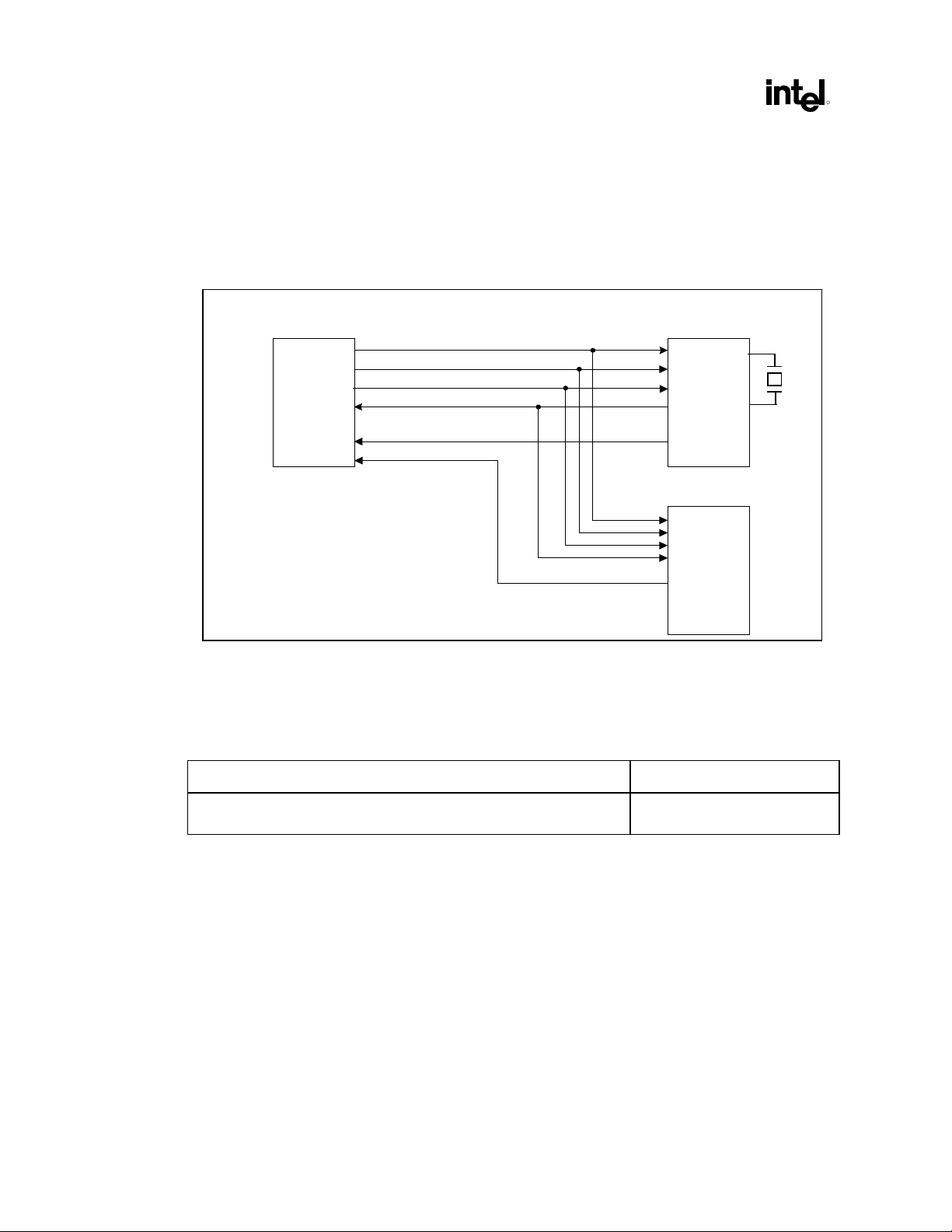
Figure 2. AC ’97 Controller Connection to Its Companion Codec
AC'97 Digital
Controller
RESET#
SDATA_OUT
AC '97
controller
section of
the ICH
SDATA_IN_0
SDATA_IN_1
SYNC
BIT_CLK
R
Primary
Codec
Secondary
Codec
This document specifies only the software requirements and the driver interface for the Intel® ICH AC
’97 digital controller.
1.1. Reference Documents and Information Sources
Document Name Available From
Intel® 82801AA (ICH) or Intel® 82801AB (ICH0) I/O Controller Hub
Datasheet
Order number: 290655
8 Programmer’s Reference Manual

Intel® 82801AA (ICH) & Intel® 82801AB (ICH0) I/O Controller Hub AC ’97
R
2. AC ’97 Controller’s Theory of Operation
The ICH AC ’97 Digital Controller (DC) interface is an implementation of the AC ’97 Link, with
additional features for supporting transaction and device power management. The AC ’97 DC includes
DMA engines for high-performance data transfer to memory, via a hub interface.
AC ’97 DC and link supports isochronous traffic, which emphasizes data timing. This is critical for
maintaining the data stream from the audio and/or modem codec.
2.1. AC’97 Initialization
2.1.1. System Reset
The AC ’97 circuitry is reset upon power-up, by combining the PCIRST# signal with the AC Link
RESET# signal. However, AC Link RESET# will not follow PCIRST# during a resume-from-sleep
condition. During operation, the system can be reset by clearing the AC ’97 Cold Reset bit in the Global
Control/Status register (NABMBAR + 60h). This bit is maintained during the ICH sleep mode and can
be used by the driver to select a warm or cold reset during a resume condition. If the codec is not present
(i.e., AC '97 is not supported), codec ready will never be seen by the controller. Once the reset has
occurred, a read to Mixer register 00h/80h will indicate the type of hardware residing in the codec(s).
Note: It is good practice to always check the Codec Ready bit before accessing the mixer register for the first
time.
Programmer’s Reference Manual 9

Intel® 82801AA (ICH) & Intel® 82801AB (ICH0) I/O Controller Hub AC ’97
2.1.2. Codec Topology
The following figure shows the allowable codec configuration when attaching to the ICH AC ’97 link.
To avoid improper driver loading, the system BIOS should determine the presence/absence of the audio
or modem codec attached on the AC link. (See Appendix A for the detailed procedure.)
Figure 3. Possible Codec Configurations
R
1. Single-Codec Audio
AC Audio
®
Intel
801
AC '97
Controller
3. Single-Codec Audio/Modem
Intel® 801
Audio/Modem
AC '97
Controller
Codec
AMC
Codec
2. Single-Codec Modem
MC Modem
®
Intel
801
Codec
AC '97
Controller
4. Dual-Codec Audio and Modem
Intel® 801
AC '97
Audio Codec
Controller
MC Modem
Codec
AC
codec_config
This information is used to disable (i.e., hide) the appropriate PCI function. To determine whether a
codec or codecs are attached to the link, the system BIOS uses the following procedure.
10 Programmer’s Reference Manual

Intel® 82801AA (ICH) & Intel® 82801AB (ICH0) I/O Controller Hub AC ’97
R
2.1.3. BIOS PCI Configuration
As previously indicated, the AC ’97 controller exposes two PCI functions in ICH device 31h. This allows
for driver differentiation between these capabilities in the component.
• Function 5: AC ’97 audio controller
• Function 6: AC ’97 modem controller
As PCI devices, there are a number of registers that must be initialized in order to enable these functions.
The following table summarizes these requirements.
Table 1. Audio Registers (Device 31 Function 5 Audio)
Offset Register Default Initialize Comments
04h–05h Command (COM) 0000h 0005h Bit 2: Bus Master Enable
10h–13h Native Audio Mixer Base
Address
14h–17h Native Audio Bus
Mastering Base Address
3Ch Int errupt Line (INTLN) 00h 0Zh A hardware interrupt (0-Fh) that
00000001h 0000XX01h 0xXX00: Address in the 64-KB I/O
00000001h 0000YY01h 0xYY00: Address in the 64-KB I / O
Bit 0: I/O Space Enabl e
space that allows 256 bytes of
registers not in confli ct with any
other set
space that allows 256 bytes of
registers not in confli ct with any
other set
follows the value assigned to
PIRQB#. It has no eff e ct on ICH and
is used to indicate to software the
IRQ value assigned to the device.
Programmer’s Reference Manual 11

Intel® 82801AA (ICH) & Intel® 82801AB (ICH0) I/O Controller Hub AC ’97
Table 2. Modem Registers (Device 31 Function 6 Modem)
Offset Register Default Initialize Comments
R
04h–05h Command (COM) 0000h 0005h Bit 2: Bus Master Enable
10h–13h Native Audio Mixer Base
Address
14h–17h Native Audio Bus
Mastering Base Address
3Ch Interrupt Line (INTLN) 00h 0Zh A hardware interrupt (0–Fh)
A PnP-capable OS is responsible for initializing these PCI registers. If a PnP OS is not available in the
system, then the BIOS is responsible for configuring all PCI devices, including these registers. A switch
in the system setup usually is used to determine whether PnP is present. However, the final configuration
and the existence/absence of this switch is implementation dependent.
2.1.4. Hardware Interrupt Routing
Bit 0: I/O Space Enabl e
00000001h 0000XX01h 0xXX00: Address in the 64-KB
I/O space that allows 256
bytes of registers not i n
conflict with any other set
00000001h 0000YY01h 0xYY00: Address in the 64-KB
I/O space that allows 256
bytes of registers not i n
conflict with any other set
that follows the value
assigned to PIRQB#. I t has no
effect on ICH and is used t o
indicate to software the IRQ
value assigned to the device.
The audio and modem functions in the ICH internally share the same PCI IRQ (PIRQB#). The
configuration software must take this into account and assign the same IRQ pin to both functions.
Sharing IRQs increases the ISR latencies. Each ISR must determine if the interrupting device is the one
serviced by the routine. If the device does not belong to the current servicing ISR, the ISR is responsible
for calling the next ISR in the chain. PIRQB# also is exposed as a PCI interrupt on the PCI slots.
Therefore, a device installed in a PCI slot may use the same IRQ assigned to the AC ’97 functions. This
further increases the ISR latencies.
In an environment were a high Quality of Service (QoS) is required, system designers must pay close
attention to devices attached to the same PIRQ. Software-driven signal processing functions, such as in
the case of software-driven modem and audio, require the maintenance of a low latency interrupt service,
in order to maintain the proper functionality. Software driver programmers must pay close attention to
the ISR latencies and make use of DPC, as much as possible.
2.2. DMA Engines
The ICH AC ’97 controller uses the scatter/gather mechanism to access memory. There are three 16-bit
DMA engines for audio PCM stereo in, PCM stereo out, and MIC mono. There are two 16-bit DMA
engines for modem in and modem out. The audio and modem registers are located in two separate PCI
functions in the ICH components, in order to allow for driver flexibility.
12 Programmer’s Reference Manual

Intel® 82801AA (ICH) & Intel® 82801AB (ICH0) I/O Controller Hub AC ’97
R
2.2.1. Buffer Descriptor List
The Buffer Descriptor list is an array of up to 32 entries, each of which describes a data buffer. Each
entry contains a pointer to a data buffer, control bits, and the length of the buffer being pointed to, where
the length is expressed as the number of samples. This, combined with the 16-bit sample size, gives the
actual physical length of the buffer. The buffer length is restricted to 65536 samples. “0” in the buffer
length indicates no samples to process. Each descriptor can point to a buffer of a different size. The
samples are stored two per DWord (16-bit samples). In the case of audio PCM, these represent the left
and right channels, respectively.
Figure 4. Generic Form of Buffer Descriptor (One Entry in the List)
(DWord 0 : 00–03h)
31 1 0
Buffer Pointer 0
(DWord 1 : 04–07h)
31 30 29 16 15 0
IOC BUP R Buffer Length
Table 3. BD Buffer Pointer (DWord 0: 00–03h)
Bit Description
31:1 Buffer pointer. This field points to the l ocation of the data buffer. S i nce samples can be as wide as one
word, the buffer must be aligned with word boundaries, to prevent samples from straddling DWord
boundaries.
0 Reserved. Must be 0 when writing this field.
Table 4. BD Control and Length (DWord 1: 04–07h)
Bit Description
31 Interrupt On Completion (IOC).
1 = Enabled. When this is set, it means that t he controller should issue an int errupt upon completion of
this buffer. It should also set the IOC bit i n the status register.
0 = Disabled.
30 Buffer Underrun Policy (BUP).
0 = When t hi s buffer is compl ete, if the next buffer is not yet ready (i .e., the last valid buffer has been
processed), then continue to transmit the last valid sample.
1 = When t hi s buffer is compl ete, if this is t he l ast valid buffer, transmit zeros after thi s buffer has been
processed complet el y. Thi s bit typically is s et only if this is the l ast buffer in the current stream.
29:16 Reserved. Must be 0 when writing this field.
15:0 Buffer length. This is the length of the data buff er, in number of samples. The controller uses t hi s data
to determine the length of the buffer, in bytes. “0” indi cates no sample to process.
Programmer’s Reference Manual 13

Intel® 82801AA (ICH) & Intel® 82801AB (ICH0) I/O Controller Hub AC ’97
2.2.2. DMA Initialization
The maximum length of the buffer descriptor list is fixed at 32. (This is limited by the size of the index
registers.) The figure below shows the organization of the Buffer Descriptor List.
Figure 5. Buffer Descriptor List
R
Buffer Description List
Base Address
Buffer Pointer
Command Length
Buffer Pointer
Command Length
Buffer Pointer
Command Length
Buffer Pointer
Command Length
Buffer Pointer
Command Length
Data Buffer
Current Index
n - 1
Prefetched Index
n
Last Valid
n + 1
buf_desc_list
The following steps describe the driver initialization process for a single DMA engine. The same process
should be repeated for each DMA engine.
1. Create the buffer descriptor list structure in memory (non-paged poll).
2. Write the Buffer Descriptor List Base Address register with the base address of the buffer descriptor
list.
Table 5. Audio Descriptor List Base Address
Audio Buffer Descriptor List Base Address I/O Address
PCM IN NABMBAR + 00h (PIBDBAR)
PCM OUT NABMBAR + 10h (POBDBAR),
MIC NABMBAR + 20h (MCBDBAR)
14 Programmer’s Reference Manual

Intel® 82801AA (ICH) & Intel® 82801AB (ICH0) I/O Controller Hub AC ’97
R
Table 6. Modem Descriptor List Base Address
Modem Buffer Descriptor List Base Address I/O Address
Line IN MBAR + 00h (MIBDBAR)
Line OUT MBAR + 10h (MOBDBAR),
3. Set up the buffer descriptors and their corresponding buffers. Buffers are passed to the mini-port
driver as Memory Descriptor Lists (MDL). These MDLs contain the physical page address of the
virtual audio buffer. Multiple buffer descriptors may be required to represent a single virtual buffer
passed to the mini-port driver. PCM buffers always must be of even length, since they are always in
stereo.
4. Once buffer descriptors have been set in memory, the software writes the Last Valid Index (LVI)
register.
Table 7. Audio Last Valid Index
Audio Last Valid Index (LVI) I/O Address
PCM IN NABMBAR + 05h (PILVI)
PCM OUT NABMBAR + 15h (POLVI)
MIC NABMBAR + 25h (MCLVI)
Table 8. Modem Last Valid Index
Modem Last Valid Index (LVI) I/O Address
Line IN MBAR + 05h (MILVI)
Line OUT MBAR + 15h (MOLVI)
5. After the LVI registers have been updated, the software sets the run bit in the control register, in
order to execute the descriptor list.
2.2.3. DMA Steady-State Operation
Software has two concurrent activities to perform during normal operation: Preparing new buffers/buffer
descriptors and marking as free the processed buffer descriptors and buffers. Once the run bit has been
set in bus master control register bit 0, the bus master fetches the buffer descripto r.
1. The bus master starts processing the current buffer. Once current buffer has been processed,
depending upon the bits set in the command field, the interrupt is asserted and the interrupt bit is set.
2. The bus master increments the current and prefetch indices. It then starts executing the current buffer
and schedules the next buffer to be prefetched.
3. The buffer service routine maintains a variable that points to the head of the list of descriptors to be
processed. The descriptor list service routine performs the following activities:
Programmer’s Reference Manual 15

Intel® 82801AA (ICH) & Intel® 82801AB (ICH0) I/O Controller Hub AC ’97
// Update head of descriptors to be processed
While (head != current_index)
{
Mark head free ;
// Check for end of descriptor list
If head == base_address + (31 * 8);
// Last entry on the list, set head to top of list
head = base_address;
Else
// Still inside list, increment head to next entry
head++;
}
Note: This algorithm needs to be optimized in order to reduce the number of memory accesses during
execution. The While statement could translate to several memory accesses, if this code is not executed
after each buffer descriptor update.
Also, the routine that prepares buffers maintains a variable that points to the entry after the tail of the list.
This value is always the next entry after the Last Valid Index register. This routine utilizes the following
algorithm:
R
// Update tail of descriptor list ready for execution
// and audio buffers when available for processing
While ((
tail == free) && (buffers_available > 0))
{
Prepare buffer descriptor indexed by
tail;
buffers_available--;
//Assign tail to Last Valid Index
LVI = Tail;
// Check for end of descriptor list
If (tail == base_address + 31 * 8);
// Last entry on the list, set tail to top of list
tail = base_address;
Else
// Advance tail to next value
tail++;
}
16 Programmer’s Reference Manual

Intel® 82801AA (ICH) & Intel® 82801AB (ICH0) I/O Controller Hub AC ’97
R
2.2.4. Stopping Transfers
There are two ways to stop transfers:
1. Simply turn off the Bus Master run/pause bit. This will immediately halt the current DMA transfer.
Data in the output FIFOs will be read out until they empty. The registers will retain their current
values and the AC link’s corresponding slots will be invalidated. Setting the run/pause bit will
resume DMA activity.
2. Software can stop creating new buffers and hence not update the Last Valid Index register. The bus
master will stop once the last valid buffer has been processed. All register information is maintained.
During this condition, the controller will transmit the last valid sample or zeros, depending on the
status of the Buffer Underrun Policy (BUP) bit in the buffer descriptor entry. If the run/pause bit
remains set, then any future update to the Last Valid Index register will cause the bus master
operation to resume.
Note: Software must ensure that the DMA controller halted bit is set before attempting to reset registers.
2.2.5. FIFO Error Condi tions
Two general conditions could cause FIFO error bit 4 in the status register to be set. Depending on the
status of bit 3 in the control register, this also causes an interrupt.
2.2.5.1. FIFO Underrun
FIFO underrun will occur when the AC ’97 controller FIFO is drained.
1. This results from system congestion. The DMA read transaction could still be pending, as data has
not returned from memory. In this case, the controller will repeat the last sample until new data is
available in the FIFO.
2. As a result of the DMA engine reaching the Last Valid Index, there is no further access to memory.
Therefore, the FIFO will drain. In this case, the controller will transmit the last valid sample or zeros,
depending on the status of the Buffer Underrun Policy (BUP) bit in the buffer descriptor entry. This
condition is an error unless the software is able to update the descriptor list before the DMA engine
reaches the Last Valid Index. However, this condition could result from the completion of the
processing of the last buffer. It is up to the software driver to determine the final status of this
condition. Also see the preceding Stopping Transfers section.
Programmer’s Reference Manual 17

Intel® 82801AA (ICH) & Intel® 82801AB (ICH0) I/O Controller Hub AC ’97
2.2.5.2. FIFO Overrun
FIFO overrun occurs when valid data is transmitted in proper AC link slots and the DMA FIFO remains
full. Two conditions could cause FIFO error bit 4 in the status register to be set. Depending on the status
of bit 3 in the control register, this also will cause an interrupt.
1. This results when the DMA engine is unable to update system memory with the contents of the FIFO,
as a result of system congestion. In this case, all new samples received from the AC Link will be lost.
2. When the DMA engine reaches the last valid index, there is no further access to memory. Therefore,
the FIFO will not drain. This condition is an error if the software is unable to update the descriptor
list before the DMA engine reaches the last valid index. However, this condition could result
naturally when the last buffer entry has been processed. It is up to the software driver to determine
the final status of this condition. Also see the preceding Stopping Transfers section.
2.3. Arbitration
Up to five AC '97 DMA channels can be enabled at one time: PCM in, PCM out, Mic in, Modem in, and
Modem out. A round-robin arbitratio n scheme is used to arbitrate a mong t he five channels.
R
2.4. Data Buffers
2.4.1. Memory Organization of Data
The 16-bit samples are packed in, with two samples per DWord. The buffers are always DWord aligned.
2.4.2. FIFO Organization
The ICH AC '97 controller supports 16-bit samples on all channels.
Data is written to the FIFO in sample pairs, according to the order of valid slots in a channel. For
example, for audio PCM in, the controller checks the first valid slot and adds it to the FIFO first entry as
a word (16 bits). The next valid slot is added as the second word entry in the FIFO, in order to create the
PCM stereo sample pair. This procedure assumes that the first valid slot always is the left channel
(slot 3), followed by the right channel in slot 4 in the same or subsequent frame. If the codec transmits
data repeating the slot, this will cause the controller to misplace the sample in the FIFO. Codecs
compatible with the ICH AC ’97 implementation should always maintain the indicated order, and should
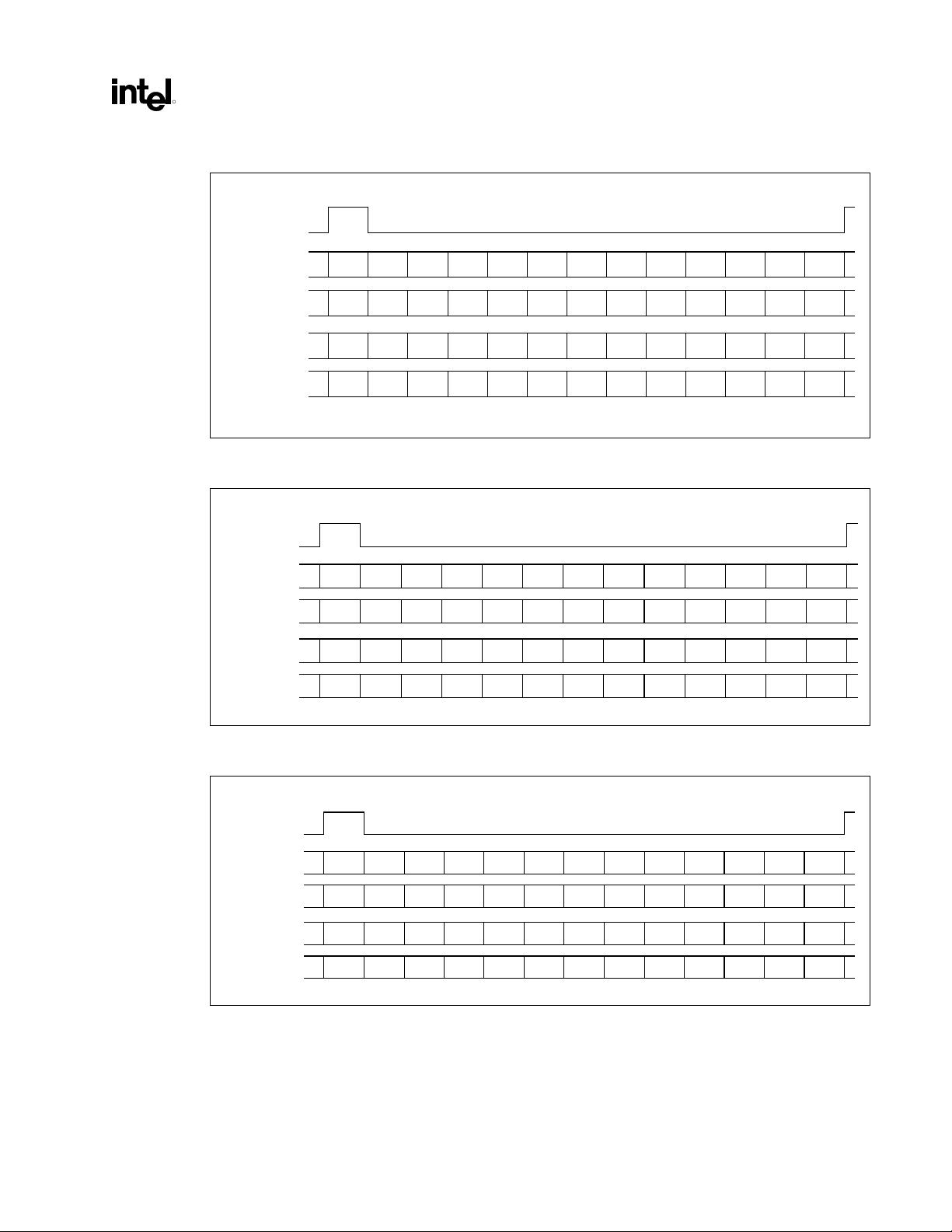
never use the same slot twice in order to transmit samples to the controller. The figures below show
ICH-compatible and ICH-incompatible implementations.
18 Programmer’s Reference Manual
Intel® 82801AA (ICH) & Intel® 82801AB (ICH0) I/O Controller Hub AC ’97
R
Figure 6. Compatible Implementation with Left and Right Sample Pair in Slots 3 and 4 Every Frame
Slot #
SYNC
0123456789101112
Frame n
Frame n + 1
Frame n + 2
Frame n + 3
TAG
TAG
TAG
TAG
CMD
ADR
STATUS
ADR
CMD
ADR
STATUS
ADR
CMD
DATA
STATUS
DATA
CMD
DATA
STATUS
DATA
XX
X
X
X
MDM
CDC
MDM
X
CDC
MDM
X
CDC
MDM
X
CDC
RSRVD
RSRVD
RSRVD RSRVD RSRVD RSRVD RSRVD
MIC
RSRVD RSRVD RSRVD RSRVD
RSRVDRSRVD
RSRVD RSRVD RSRVD RSRVD RSRVD
MIC
RSRVD
RSRVDRSRVDRSRVD
I/O
control
I/O
Status
I/O
control
I/O
Status
frame_1
Figure 7. Compatible Implementation with Sample Rate Conversion Slots 3 and 4 Alter nating over
Next Frame
Slot #
SYNC
Frame n
Frame n + 1
Frame n + 2
Frame n + 3
0123456789101112
TAG
TAG
TAG
TAG
CMD
ADR
STATUS
ADR
CMD
ADR
STATUS
ADR
CMD
DATA
STATUS
DATA
CMD
DATA
STATUS
DATA
X
X
MDM
CDC
MDM
X
X
CDC
MDM
CDC
MDM
CDC
MIC
MIC
RSRVD RSRVD RSRVD RSRVD
RSRVDRSRVD
RSRVD RSRVD RSRVD RSRVD RSRVD
RSRVD RSRVD RSRVD RSRVD
RSRVDRSRVD
RSRVD RSRVD RSRVD RSRVD RSRVD
I/O
control
I/O
Status
I/O
control
I/O
Status
frame_2
Figure 8. Incompatible Implementation of Sample Rate Conversion with Repeating Slots over Next
Frames
Slot #
SYNC
Frame n
Frame n + 1
Frame n + 2
Frame n + 3
0123456789101112
TAG
TAG
TAG
TAG
CMD
ADR
STATUS
ADR
CMD
ADR
STATUS
ADR
CMD
DATA
STATUS
DATA
CMD
DATA
STATUS
DATA
X
X
MDM
CDC
MDM
X
CDC
MDM
X
CDC
MDM
CDC
RSRVDRSRVD
RSRVD RSRVD RSRVD RSRVD
RSRVD RSRVD RSRVD RSRVD RSRVD
MIC
RSRVD RSRVD RSRVD RSRVD
RSRVDRSRVD
RSRVD RSRVD RSRVD RSRVD RSRVD
MIC
I/O
control
I/O
Status
I/O
control
I/O
Status
frame_3
Programmer’s Reference Manual 19

Intel® 82801AA (ICH) & Intel® 82801AB (ICH0) I/O Controller Hub AC ’97
Table 9. FIFO Summary
Channel No. of Samples FIFO Depth FIFO Width Comments
Mic In 1 2 32 bits Two samples per entry (DWord)
PCM In 2 4 32 bits Left and right for stereo in the same
PCM Out 2 4 32 bits Left and right for stereo in the same
Modem In 1 2 32 bits Two samples per entry (DWord)
Modem Out 1 2 32 bits Two samples per entry (DWord)
2.5. Multiple Codec/Driver Support
The ICH AC ’97 controller is capable of supporting a two-codec implementation. Under this
implementation, both codecs share the SDATA_OUT signal, while independent SDATA_IN[0:1] are
used by the codec to supply data to the controller. Even when two SDATA_IN are used, these two
signals are logically ORed inside the digital controller, effectively creating one digital input data stream.
This configuration precludes the simultaneous use of two similar codecs. Therefore, only one audio and
one modem function are allowed to operate concurrently.
R
FIFO. Two samples per DWord
FIFO. Two samples per DWord
2.5.1. Codec Register Read
Codec register reads are presented in the AC link in the next available frame after the I/O transaction is
received by the controller. Data is returned to the controller, depending on codec availability. In the
meantime, the processor waits for the transaction to complete, thereby stalling further software execution.
To avoid longer-than-necessary latencies, the codec must return data in the next-available frame.
Multiple frame transactions impose large system latencies, to the detriment of system performance.
Even when data is returned in the frame immediately after the read request is presented in the AC link,
the minimum latency is still on the order of 40 µs. To minimize the effect on the system caused by long
latencies in the AC link, the software drivers must maintain a copy of the codec register in memory (i.e.,
shadow) and must use this data instead of accessing the codec.
Shadowing in memory is effective as long as the codec does not change the register values themselves.
Therefore, the status of the GPIOs configured as inputs on the latest frame is accessible to software, by
reading the register at offset 54h in the modem codec I/O space. Only the 16 MSBs are used to return
GPI status. Reads from 54h will not be transmitted across the link. Instead, data received in slot 12 is
stored internally in the controller, and the data from the most recent slot 12 is returned on reads from
offset 54h.
Power-down in the codec offset 26h and 3Eh status registers is not supported by an automatic shadowing
mechanism, as is the case for offset 54h. However, these registers are used sparingly and are read only
during power-down status determination.
Finally, the codec ready status is required during system initialization. It is automatically reflected in the
Global Status Register at NABMBAR + 30h (MBAR + 40h) bit 8 for the primary codec and at bit 9 for
the secondary codec. These two bits need not be saved in memory.
20 Programmer’s Reference Manual

Intel® 82801AA (ICH) & Intel® 82801AB (ICH0) I/O Controller Hub AC ’97
R
2.5.2. Codec Access Synchronization
All codec register writes are posted transactions in the AC ’97 controller. The AC ’97 controller
indicates transaction completion to the host processor immediately following the request, even when the
transaction is actually pending completion in the AC link. This is done to improve system performance.
However, it also restricts the operation of the driver(s). Also, register reads present synchronization
issues.
Before a codec register access is initiated, the driver must check the status of the codec access in
Progress (CAIP) bit 0, in the Codec Access Register at NABMBAR + 34h (MBAR + 44h). If no write is
in progress, this bit will be 0, and the act of reading the register sets this bit to 1. This reserves the right
to perform I/O read or write access. Once the write is completed, hardware automatically clears the bit.
The driver also must clear this bit, if it decides not to perform a codec I/O write after reading this bit. If
the bit has already been set, it indicates that another driver is performing a codec I/O write across the
link, so the driver should try again later.
2.6. Power Management
Power management of the driver/codec interaction requires careful sequencing in the AC ‘97
environment. In the ICH AC ‘97 environment, it is possible for two drivers to share the same AC link
interface with two separate codecs. If a driver forces an aggressive sleep state in the link, it could have
functional repercussions on the pairing codec. The D3 state is the deep sleep state in a device that abides
by ACPI compliance requirements. When a driver is requested to set its device to the D3 state, the driver
should enter the most aggressive power-saving mode possible. The D3 state also is often the precursor to
a system-wide core power removal. Therefore several considerations must be taken into account, in order
to maintain the device functionality and wake-up capability.
The procedure followed by an AC ‘97 device driver varies according to the system configuration. The
following table lists the possible codec combinations supported by the ICH AC ‘97 controller.
The Intel
®
ICH audio/modem controller supports a maximum of one audio and one modem device. The
following system implementations are possible. (For details, also see Figure 3. Possible Codec
Configurations.)
Table 10. Codec Topologies
Configuration
1 AC (primary)
2 MC (primary)
3 AC (primary) + MC (secondary) Possible D3 state interactions
4 AMC (primary) Possible D3 state i nteractions
Note: These configurations could be limited further by the AC ‘97 riser card configuration and loading. For
details, refer to the Audio/Modem I/O Riser Specification.
It is evident that configurations 1 and 2 require no driver synchronization among AC ‘97 codecs.
Configurations 1 and 2 are single-codec topologies. Therefore, an aggressive power-saving mode is
possible, including the disabling of the actual AC link without the risk affecting paired-codec
functionality. Configuration 3, however, is a two-codec topology. In Configuration 3, an aggressive
power-saving mode requires detailed attention, in order to avoid driver interactions and their effect on
the AC link functionality. Configuration 4 is a single-codec topology that provides both audio and
Programmer’s Reference Manual 21

Intel® 82801AA (ICH) & Intel® 82801AB (ICH0) I/O Controller Hub AC ’97
modem functions. In this configuration, driver interaction also is critical if a separate set of drivers is in
control of the audio and modem functions.
To manage the power of AC ‘97 codecs, there are two sets of PR bits of concern to drivers. One set at
offset NAMBAR + 26h in the audio function maps to offset 26h in the primary codec, and a second set at
MMBAR + 3Eh maps to offset 3Eh in the modem function. Note that register 3Eh does not provide linkdown functionality, which is provided in the register 56h bit 12 (MLNK) modem link.
2.6.1. Power Management Transition Maps
The following paragraphs discuss power management transition maps, within the constraints of an ACPI
system environment. The following tables map a codec’s PR bit transitions to specific ACPI D states for
the device.
The following points were taken into considera tion when generating the following tables:
• Power management is defined within the framework of a desktop system. Furt her power savings are
possible by implementi ng more aggressive power management typical of mobile environment
policies. (See the following Aggressive Power Management section.) However, these power savings
are a trade-off between the driver complexity and the functional restrictions.
R
• The selection of a specific power policy depends on the proper identification of the topology by the
driver(s).
• The secondary codec is provided with an external clocking mechanism and is not dependent on
BIT_CLK to drive internal state machines, when in the power-down mode.
• After a warm or cold reset, the device driver brings all PR(x) bits to the D0 state.
• The transition from/to any Dx state is accomplished by simultaneously setting/resetting all
appropriate PR(x) bits. The codec should not limit the PR(x) bit transition sequence discussed
previously.
• Audio Codec Reg. 26h D15 EAPD (formerly, the PR<7> enable/disable function) is newly defined
as the control for an external audio power amp. The audio codec should provide an audio amp
output pin (GPO) that provides off/on capability according to this bit’s set/reset status.
• The modem tables assume caller-ID capability during wake-up-on-ring, so Vref is ON during D3.
• The modem D3 configuration is dependent upon wake-up-on-ring event enable. If wake-up-on-ring
is enabled, the GPIO cannot go down in D3.
Note: When a codec section is powered back on, the Powerdown Control/Status register (index 26h) should be
read to verify that the section is ready, before attempting any further operations.
22 Programmer’s Reference Manual

Intel® 82801AA (ICH) & Intel® 82801AB (ICH0) I/O Controller Hub AC ’97
R
Configuration 1 single audio codec - primary:
Table 11. Power State Mapping for Audio Single-Codec Desktop Transition
PR<0:5> + (EAPD) +12 +5
from
+12
+3.3
Digital
+3.3
Vaux
Digital
Comments
EAPD CLK AC-
Device
State
D0 0 000000OnOnOnOnAll on
D1 0 000011On On On On DAC, ADC
D2 1 0001 1 1 On On On On Mix, Amp
D3 1 1111 1 1 Off Off Off On Clock, Vref
7 543210
Link
Mixer
Vref.
Mixer DAC ADC
Configuration 2 single-modem codec - primary:
Table 12. Power State Mapping for Modem Single-Codec Desktop Transition
(other power control (PRx) bits do not apply for ICH
Device State MLNK D C B A
D0 0 0 0 0 0 On On On On All on
D1 0 11 0 0 On On On On DAC, ADC
D2 0 1 1 0 0 On On On On Same as D1
D3 (wake-up
on ring)
D3 1 11 11Off Off Off On Sdata_In, Vref,
PR<A:D> + MLNK
implementation)
Sdata_In DAC1 ADC1 Vref GPIO
1 1 1 0 0 Off Off Off On Sdata_In
+12 +5
from
+12
+3.3
Digital
+3.3
Vaux
Digital
Comments
GPIO
Programmer’s Reference Manual 23

Intel® 82801AA (ICH) & Intel® 82801AB (ICH0) I/O Controller Hub AC ’97
Configurations 3 and 4 dual-func tion, single- or dual-codec configuratio n:
Table 13. Power State Mapping for Audio in Dual-Codec Desktop Transition
PR<0:5> + (EAPD) +12 +5
from
+12
+3.3
Digital
+3.3
Vaux
Digital
R
Comments
EAPD CLK AC-
Device
State
D0 0 000000OnOnOnOnAll on
D1 0 000011On On On On DAC, ADC
D2 1 0001 1 1 On On On On Mix, Amp
D3 1 0 0 1 1 1 1 Off Off Off On Clock, Vref
7 543210
Link
Mixer
Vref.
Mixer DAC ADC
1. PR(4) link-down and PR(5) internal clocks disable are NOT recommended for desktop
configuration. Setting these to power control bits could affect modem operation in an AC + MC
configuration.
2. In a mobile system configuration, PR(4) and PR(5) could be used to provide further power savings.
Driver designers should use D3 state codec semaphores in the ICH AC ‘97 controller, in order to
determine the audio or modem codec power status before setting the PR(4) and PR(5) bits. For
details, refer to the ICH AC ‘97 External Architecture Specification. The mini-port driver developed
for the ICH AC ‘97 controller does not provide this capability.
Table 14. Power State Mapping for Modem in Dual-Codec Desktop Transition
(other power control (PRx) bits do not apply for ICH
PR<A:D> + MLNK
implementation)
+12 +5
from
+12
+3.3
Digital
+3.3
Vaux
Digital
Comments
Sdata_In DAC1 ADC1 Vref GPIO
Device
State
D0 0 0 0 0 0 On On On On All on
D1 0 110 0 On On On On DAC, ADC
D2 0 1 1 0 0 On On On On Same as D1
D3 (wake-
up on ring)
D3 1 1111Off Off Off On Sdata_In, Vref, GPIO
MLNKDCB A
1 1 1 0 0 Off Off Off On Sdata_In
24 Programmer’s Reference Manual

Intel® 82801AA (ICH) & Intel® 82801AB (ICH0) I/O Controller Hub AC ’97
R
Tables 10 and 11 show the recommended power transition tables for a desktop system. The preceding
tables eliminate the need for a driver to provide codec topology detection, thereby simplifying the
initialization sequence. These tables do not provide the maximum power saving. However, they are
believed to provide sufficient power saving for desktop applications. The OEM and IHV are free to
differentiate their products further by enabling the deeper power savings obtained by identifying the
codec topology.
2.6.2. Topology Detection
A set of drivers could always assume the preceding configurations 3 and 4 and establish their power
management policy based on Tables 10 and 11. These are the safest configurations, with a semiaggressive power management st yle consistent with a desktop environment. However, even in a desktop
environment, further power savings are possible when in single-codec configurations 1 and 2. In order to
implement the preceding tables, the audio driver must be able to predetermine the AC link topology
configuration.
2.6.2.1. Determining the Presence of a Secondary Codec
To determine whether or not a secondary codec is present, the driver must check the secondary codec
ready bit located in the Global Status Register at:
Secondary Codec Ready: I/O Address: NABMBAR + 30h (MBAR +40h), bit 9
If this bit is set to 1, it indicates that a secondary codec is active in the AC link.
2.6.2.2. Determining the Presence of a Modem Function
In the case of an AMC configuration, only the primary codec ready bit is indicated. In order to determine
the proper power-down configuration, the audio driver must determine the presence/absence of modem
functionality in the codec. The audio driver could check the Extended Modem ID Register at:
Extended Modem ID: I/O Address: NAMBAR + 3Ch
The content of this register is FFh, if no modem function is present.
2.6.3. Aggressive Power Management
As indicated in previous sections, it is possible to go into a more-aggressive power-saving mode by
carefully synchronizing the audio and modem driver interactions over the AC link. This aggressive
power saving usually is found in mobile environments, where battery power is critical.
Driver synchronization is required in a dual-codec configuration, where the audio driver could cause a
link-down power condition, by setting the PR4 and PR5 bits in the audio codec register. When PR4 and
PR5 are set, the AC link base clock BIT_CLK is stopped. If this action occurs while the modem codec is
still in the operating mode, it will cause malfunctions and possibly hang the system.
Programmer’s Reference Manual 25

Intel® 82801AA (ICH) & Intel® 82801AB (ICH0) I/O Controller Hub AC ’97
To avoid this and similar situations, the audio and modem driver could follow a protocol using the
provided audio and modem D3 state bit semaphores: AD3 for audio and MD3 for modem. These bits are
located at:
Codec Write Semaphore Registers:
NABMAR + 30h audio I/O space and MBAR + 40h modem I/O space
Bit 16 for audio (AD3)
Bit 17 for modem (MD3)
The AC ’97 drivers should set the appropriate bit after setting the codec in the D3 state. The audio codec
could use this semaphore to determine if the modem codec is already in the D3 state and to shut down the
link by also asserting PR4 and PR5 in the power management register in the audio function/codec. The
following sections review in detail the sequence of events for drivers/codec entering the D3 state and
resuming the D0 state.
2.6.3.1. Primary Audio Requested to Transition to D3 State
The audio power management procedure attempts to get the audio codec to transition to the D3 state.
R
If MD3 == true // (sleeping?)
{
Audio_Power_Manage_Reg = D3 + PR4 + PR5;
// yes, sleep plus AC link down
}
Else
{
Audio_Power_Manage_Reg = D3; // No, sleep keeping link up
}
AD3 = true; // Set to "audio sleeping"
// Setting the flag last avoids race condition during D0->D3 transit.
2.6.3.2. Secondary Modem Requested to Transition to D3 State
The modem power management pro cedure tries to get the modem codec to transition to the D3 state.
Secondary_codec = D3 + MLNK // Yes, sleep plus SDATA_IN1 low
MD3 = true
// Setting the flag last avoids race condition during D0->D3 transit.
// MLNK corresponds to register 56h, bit 12 (D12).
26 Programmer’s Reference Manual

Intel® 82801AA (ICH) & Intel® 82801AB (ICH0) I/O Controller Hub AC ’97
R
2.6.3.3. Secondary Modem Requested to Transition to D0 State
The modem power management pro cedure tries to get the modem codec to transition to the D0 state.
MD3 = false // Set to "modem awake"
//Setting the flag first avoid race condition during D3->D0 transit.
If Modem_ready == True
{
Modem_Power_Manage_Reg = D0 // Bring back to fully awake.
}
If AD3 == true // (audio sleeping?)
{
Link_reset() // Cause a warm or cold reset.
While (!Modem_ready) // Wait for modem ready.
{
read modem codec ready bit every 400 ms
}
Modem_Power_Manage_Reg = D0 // Bring back to awake.
}
2.6.3.4. Audio Primary Requested to Transition to D0 State
The audio power management procedure attempts to get the audio codec
to transition to the D0 state.
AD3 = false // set to "audio awake"
//Setting the flag first avoid race condition during D3->D0 transit.
If Audio_ready == True
{
Audio_Power_Manage_Reg = D0; //Bring back to fully awake.
}
If MD3 == true; // (modem sleeping?)
{
Link_reset(); // Cause a warm or cold reset.
While (!Audio_ready); // Wait for modem ready.
{
read audio codec ready bit every 100ms;
}
Audio_Power_Manage_Reg = D0; // Bring back to awake.
}
Appendix B provides a schematic representation of the wake-up circuitry. This should be used as the
reference for ACPI and APM wake-up code, since it relates to the preceding paragraph.
Programmer’s Reference Manual 27

Intel® 82801AA (ICH) & Intel® 82801AB (ICH0) I/O Controller Hub AC ’97
2.6.3.5. Using a Cold or Warm Reset
In the preceding pseudo code, there are several references to resetting the AC link “Link_reset()”. Before
deciding whether to execute a cold or warm reset, drivers must determine whether or not the system
enters a suspend event where core power is removed from the system. A device is in a “D3 hot” state
after the device is set in the lowest power consumption mode and the core power is maintained. A device
is in a “D3 cold” state when the device is set in the lowest power consumption mode and the core power
is removed.
In the ICH AC ’97 implementation, when core power is removed, the cold reset bit is reset to 0. This bit
is located at:
NABMBAR + 2Ch and MBAR + 3Ch
Bit 1 AC'97 Cold Reset#
A driver requested to resume the D0 state from the D3 state must check the status of the AC ’97 Cold
Reset bit. If this bit = 0, the driver sets it to 1 in order to de-assert the AC_RESET# signal in the link,
thus completing a cold reset. If the Cold Reset bit is set to 1, then a warm reset is required if the AC link
is down according to the procedures indicated under aggressive power management. To execute an AC
’97 warm reset, the driver must set to 1 the AC ’97 Warm Reset bit located at:
R
NABMBAR + 2Ch and MBAR + 3Ch
bit 2 AC'97 Warm Reset#
A pseudo code representation is as follows:
void Link_reset(void)
{
If Cold_Reset# == True // AC_RESET# asserted, D3 when cold!
{
Cold_Reset# = False; // De-assert AC_RESET# Wake-up!
}
Else
{
Warm_reset = True; // D3 is Hot! Do warm reset.
}
}
28 Programmer’s Reference Manual
Intel® 82801AA (ICH) & Intel® 82801AB (ICH0) I/O Controller Hub AC ’97
R
3. AC ’97 Audio Driver
3.1. Introduction
This section discusses one possible way to implement AC ’97 audio on an Intel chipset containing the
ICH. This document supports several different operating systems, not just Microsoft*-based operating
systems.
3.2. Win32 Driver Model
The AC ’97 DC software interface is designed for implementation as a Win32 Driver Model (WDM)
mini-port driver. WDM allows a common set of binaries for device classes and buses to be shared by
Windows* platforms that support this model (currently the Windows 98 and Windows NT* 5.0 operating
systems).
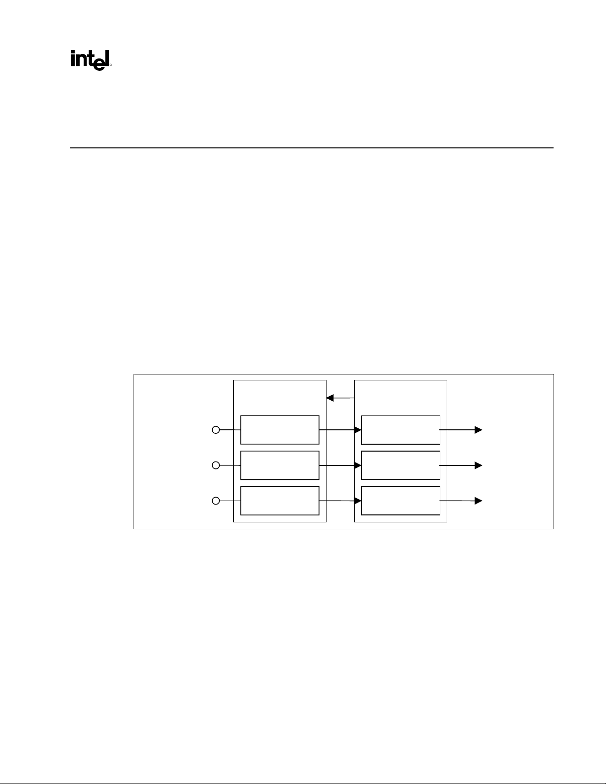
The AC ’97 DC interface under WDM should be implemented as a streaming client. The figure below
illustrates how the different layers are organized and how they interrelate:
Port Class
Driver
Port Driver
WDM
Streaming
Clients
The class driver is the highest in the chain. The bus driver (PCI) is responsible for providing an interface
to the AC ’97 audio enumeration and for loading the correct mini-port driver. The bus driver is supplied
solely by Microsoft*. The mini-port driver, which is device dependent, is responsible for sending the
commands received from the bus/class drivers onto the AC link via the host controller. For details on the
audio miniport, refer to Microsoft* Corporation’s WDM Streaming Miniport Driver Model Specification,
Rev. 0.1.
ICH AC ’97 driver is a simple WaveIn/WaveOut/MicIn driver. The operating system provides the driver
with both virtual address and physical address, along with the length of the packet. The driver has to
copy this data to the buffer descriptor, which is located in the locked memory allocated by the
miniport::Init routine using the ExAllocatePool routine. The driver must check for new b uffers (to be
sent to hardware at several different places). The driver is given the first buffer at the time the
::SetState(KSSTATE_RUN) routine gets called. Then the driver has to check for more pending buffers
during the interrupt service routine. In addition to the above two instances, the driver also can get called
by the ::MappingAvailable routine.
Port Driver
Port Driver
Adapter Driver
Miniport
Miniport
Miniport
Adapter
Hardware
Programmer’s Reference Manual 29

Intel® 82801AA (ICH) & Intel® 82801AB (ICH0) I/O Controller Hub AC ’97
3.3. Driver Organization Example
The following description is provided as reference material for supporting an ICH AC ’97 mini-port
driver. The example was developed using the Diamond Multimedia* Monster Sound PCI sound card.
The following flow diagrams (Figures 9-12) are for the Monster Sound Driver. The diagrams are based
on the driver source code provided in the Microsoft WDM DDK, Build 1676 (src\audio\monster).
The example driver contains two major C++ classes. One is associated with the Miniport Driver and
other is instantiated every time a new logical channel is created (e.g., every time a new wave file is
played).
• ADAPTER.CPP contains most of the code associated with Miniport DriverEntry and Initialization
routines. All resources (I/O, IRQ, DMA and locked memory for BTUs, which are data structures
similar to Intel’s buffer descriptors) are allocated during this phase.
• STREAM.CPP contains public and private routines of the Streams class. Key routines are SetState
(which is called by the class driver to change the current state), MappingAvailable (called by the
class driver to pass a new set of buffers), private routine ProcessNewMappings (called by
MappingAvailable, Driver ISR, and SetState to pass the pending DMA buffer to the hardware), and
New Stream (called by the class driver to create a new logical channel for a given physical channel),
and the Init routine (called by the NewStream routine).
R
The Monster Sound adapter can generate two types of interrupts: BTU and message interrupts. Both have
associated DPCs, so the ISR checks to see the source of the message, queues a DPC, clears the interrupt
at the hardware, and then returns to the kernel. The DPC routine is queued using the class driver’s Notify
routine. The DPC routine (function name Service, in Stream.cpp) releases the last processed buffer
(ProcessUnmapping) by calling the class driver's ReleaseMapping routine. Then it checks with the class
driver to see if there are any pending packets, by calling ProcessNewMappings (which calls the class
driver’s GetMappings routine).
30 Programmer’s Reference Manual

R
e
Figure 9. Sequence Overview
Intel® 82801AA (ICH) & Intel® 82801AB (ICH0) I/O Controller Hub AC ’97
High-level API call sequence
WaveOutOpen
WaveOutPrepareHeader
WaveOutWrite
ProcessNewMappings:
This routine calls ::GetMappings to get the next buffer to be sent
to the hardware. ProcessNewMappings then creates a buffer
descriptor and passes the buffer to the hardware. It also makes
sure that the hardware is still running and can process this
packet. If not, it restarts the hardware so that this packet can
beprocessed.
Miniport call sequenc
(async operations)
::NewStream
(This call retruns with an error.)
::NewStream
(This call succeeds.)
::SetState
KSSTATE_ACQUIRE
::SetState
KSSTATE_PAUSE
::SetState
KSSTATE_RUN
::ProcessNewMappings
::HwRun
::MappingAvailable
::ProcessNewMappings
DeviceI
SR
::ProcessNewMappings
seq_overview
Programmer’s Reference Manual 31

Intel® 82801AA (ICH) & Intel® 82801AB (ICH0) I/O Controller Hub AC ’97
Figure 10. Example Driver Miniport Initialization (adapter.cpp)
DriverEntry
AddDevice
StartDevice
AssignResources
NewResourceSublist
AddPortFromParent
AddInterruptFromParent
InstallSubDevice
MiniportCreate
STD_CREATE_BODY
port->Init
R
ProcessResources
NewServiceGroup
SG->AddMember
HwReset
Reset BTU Control
Reset Message Ports
Reset Midi Controller
DownloadDspCode
FindTranslatedPort
NewAccessSync
InitializeListHead
NewMasterDmaChannel
AllocateBuffer
SystemAddress
PhysicalAddress
ExAllocatePool
FindTranslatedInterrupt
NewInterruptSync
Disable Interrupts
Reset DSP
Reset GPIPs
Reset FIFO
Enable Interrupts
mini_initial
32 Programmer’s Reference Manual

Intel® 82801AA (ICH) & Intel® 82801AB (ICH0) I/O Controller Hub AC ’97
R
Figure 11. Example Streams Class Public Routines (Streams.cpp)
SetState
ControlMutex->Begin
Already in
KSSTATE_RUN ?
Yes
HwStop
Requested state
KSSTATE_RUN ?
Yes
ProcessNew Mappings
HwRun
ControlMutex->Begin
ProcessNewMappings
MapLock->Begin
AllocateHostVBTU
GetMappings
MONSTER_SETUP_VBTU
SetDirection
MONSTER_HOST_VBTU_LINK
MONSTER_SETUP_VBTU
MapLock->End
CallSynchronizedRoutine
HWRun
MONSTER_SETUP_BTU
MONSTER_HOST_VBTU_LINK
SetupFIFO
SetupBTU(DSP)
SetupBTU(HOST)
PostMessageAndWait
HWStop
PostMessageAndWait
SetupBTU(DSP)
SetupBTU(HOST)
stream_rout
Programmer’s Reference Manual 33

Intel® 82801AA (ICH) & Intel® 82801AB (ICH0) I/O Controller Hub AC ’97
Figure 12. Streams Class Public Routines (Part 2) (Streams.cpp)
R
Stream->Init
TestDataFormat()
Miniport->AddRef()
PortStream->AddRef()
NewAccessSync
AllocateHostPipe
NewServiceGroup
SG->AddMember
AllocateDSPPipe
PostMessageAndWait
NewStream
TestDataFormat()
new StreamObject
AddRef()
Stream->Init
MONSTER_SETUP_FIFO
Miniport->SetupDSPPipe
MONSTER_SETUP_BTU
stream_rout_part2
34 Programmer’s Reference Manual

Intel® 82801AA (ICH) & Intel® 82801AB (ICH0) I/O Controller Hub AC ’97
R
4. AC ’97 Modem Driver
The AC ’97 specification allows a modem codec to be connected to the AC link interface. This enables
the development of a software stack that provides modem functionality (i.e., a soft modem). Currently,
there is no single definition of how a soft mo dem should be implemented. The design problems are not
trivial for the soft modem developer. This document does not attempt to describe solutions; instead it
focuses on facilitating the development of the driver/hardware interface.
4.1. Robust Host-Based Generation of a Synchronous Data Stream
This section presents a method for reliably generating synchronous modem data on the host processor of
a computer system such that the host processor is running a non rea l -time operating system with a
maximum response latency (interrupt, thread, etc.) that exceeds the period at which the host processor
generates consecutive buffers of modem data. For the purposes of this discussion, it will be assumed that,
in response to interrupts, the host processor periodically generates a buffer of modem data in memory;
this then is utilized or consumed synchronously by hardware. This modem data consists of a sequence of
digital representations of the analog signal to be transmitted over a phone line (in accordance with one of
a variety of modem protocols, baud rates, etc.) and it could be transmitted to the AC ’97 DMA engines
via the buffer descriptor list as described in the Section 2.2, DMA Engines.
For simplicity, it also will be assumed that the data are double buffered so that failure to generate new
data before the next period will result in stream underflow (from the hardware’s viewpo int). However,
other scenarios can be accommodated, including multiple-buffering designs as well as aperiodic
processing models. The algorithm works by providing good data followed by spurious data, which is
chosen or computed so as to be adequate to maintain connection with the other modem (for example, by
transitioning seamlessly with respect to the phase of the carrier frequency and the baud rate, thereby
avoiding a retrain). This enables the datapumps of the two modems to maintain synchronization in the
face of infrequent hold-offs from processing experienced by the datapump of the host-based transmitting
modem. The spurious data will cause a packet retransmissio n or o ther action by the controller. However,
to the receiving modem, the incoming data signal will be indistinguishable from one corrupted by line
conditions.
The first invocation of the host-based modem task provides an initial buffer and one or more buffers of
spurious data (henceforth, spurious buffers). The task chooses or computes each of the spurious buffer(s)
based on the signal state at end of the immediately preceding buffer. Note that these buffers do not have
to be computed on the fly; they can be precomputed and indexed into at run time. Subsequent invocations
overwrite the previously provided spurious data with good data so that, under normal conditions, the
spurious data is never used or consumed by the DMA engine. In the event that the host-based modem
task does not generate the next buffer in time for t he DMA engine to begin consuming it, the DMA
engine is able to begin consuming the spurious buffer. In this manner, it maintains seamless connection
with the other modem’s datapump.
Programmer’s Reference Manual 35

Intel® 82801AA (ICH) & Intel® 82801AB (ICH0) I/O Controller Hub AC ’97
4.1.1. Spurious Data Algorithm
The following pseudo code presents a conceptual view of the algorithm. LastState() is a function
that returns a unique integer as a function of, for example, the carrier phase and the baud position of the
last sample in the buffer. In an actual implementation, this value is computed during the course of buffer
generation. The
while (1)
{
compute next buffer;
pNextBuffer = &buffer;
pSpuriousBuffer = &(SpuriousBufferList[LastState(buffer)]);
wait for timer interrupt;
}
In this simplified scenario, the device grabs the pNextBuffer address and stores it locally, using it to
request the samples in the buffer, one at a time. At the same time, the device copies the
pSpuriousBuffer into pNextBuffer so that when it is done with the current buffer, it will get the
spurious buffer, unless the host software runs and overwrites
data. The next section explains how to implement the spurious data algorithm within the context of the
AC ’97 buffer descriptor interface to hardware.
SpuriousBufferList is an array of precomputed spurious buffers.
pNextBuffer with a pointer to good
R
4.1.2. AC ’97 Spurious Data Implementation
The following pseudo code presents a modified version of the routine that prepares buffers and inserts
them into the AC ’97 buffer descriptor list. In contrast to the version of this routine in Section 2.2.3
(DMA Steady-State Operation), in this version
the list. Furthermore, because the AC ’97 DMA engine prefetches the next buffer descriptor, the buffer
generated by the datapump is split into two parts, with the second as small as practical. This size is called
MinBufferLength. (Here, it is assumed to be 8 samples = 4 DWords = 500 µs at 16 KHz.) For
simplicity, it is assumed that only a single buffer at a time is generated by the datapump and that there is
no checking for the end of the descriptor list (i.e., the addition is implicitly mo dulo 32).
tail points to the last good (i.e., non-spurious) buffer in
36 Programmer’s Reference Manual

Intel® 82801AA (ICH) & Intel® 82801AB (ICH0) I/O Controller Hub AC ’97
R
while (tail <= Prefetched_Index)
{
tail++; // Happens IF spurious data was used
}
if (((tail <= LastValidIndex) || (tail == free)) &&
(((tail+1) <= LastValidIndex) || ((tail+1) == free)))
{
Descriptor.BufferPtr[tail] = &buffer;
Descriptor.BufferLength[tail] =
length(buffer) – MinBufferLength;
Descriptor.BufferPtr[tail+1] =
&buffer + length(buffer) – MinBufferLength;
Descriptor.BufferLength[tail+1] = MinBufferLength;
tail += 2;
}
else
{
; //Error: no space for this data buffer
}
if ((tail <= LastValid index) || (tail == free))
Descriptor.BufferPtr[tail] =
&(SpuriousBufferList[LastState(buffer)]);
Descriptor.BufferLength[tail] =
SpuriousBufferLength[LastState(buffer)];
LastValidIndex = tail;
//Note: The tail is NOT incremented, so next time this
//descriptor will be overwritten, which is the whole point
//of this algorithm.
}
else
{
LastValidIndex = tail-1;
//Warning: no space for spurious data buffer
}
This implementation can be improved in a number of ways: Rather than adding a single (large) spurious
buffer, a number of smaller ones could be chained together. In this way, the amount of spurious data
actually transmitted would be reduced while maintaining a given level of protection against long
latencies for the host-based software. Also, the implementation could be extended to handle multiple
buffers at once, by inserting several buffers in a row, only splitting the last one, and then appending a
spurious buffer or buffers. Finally, the descriptor list is a circular buffer and a real implementation must
check
tail and tail+1 against base_address + 31 * 8.
Programmer’s Reference Manual 37

Intel® 82801AA (ICH) & Intel® 82801AB (ICH0) I/O Controller Hub AC ’97
R
This page intentionally left blank.
38 Programmer’s Reference Manual

Intel® 82801AA (ICH) & Intel® 82801AB (ICH0) I/O Controller Hub AC ’97
R
5. Appendix A: System BIOS Codec/Function Detection Algorithm
5.1. Introduction
As indicated in Section 2.1.2, Codec Topology, the system BIOS must detect the AC ’97 codec
configuration and topology before the PCI enumeration procedures. The following paragraphs describe
an algorithm that facilitates this detection process. The following provides the currently available P CI
Device IDs for the compatible Intel AC ’97 2.1 controllers:
®
Intel
82810 AC ’97 Audio Controller 2415h
®
Intel
82810 AC ’97 Modem Controller 2416h
®
Intel
82820 AC ’97 Audio Controller 2425h
®
Intel
82820 AC ’97 Modem Controller 2426h
5.2. Pre-Boot PCI Audio/Modem Enabling Matrix
PCI Hide Functi on Register Dev. 31, Func. 0, Offset F2h
Bit 5: When set hides the audio function (dev. 31, func. 5)
Bit 6: When set hides the modem function (dev. 31, func. 6)
During POST and before PCI enumeration, BIOS should determine the codec configuration and disable
PCI audio or modem as listed in the following table.
Table 15. PCI Functions Enable/Disable
Configuration
vs. Function
PCI Dev 31,
Func. 5 (audio)
PCI Dev. 31,
Func. 6 (modem)
#0
No Codec#1Single Audio
Codec
(SDATA_IN_0)
Disable ✗ Enable ✓ Disable ✗ Enable ✓ Enable ✓
Disable ✗ Disable ✗ Enable ✓ Enable ✓ Enable ✓
#2
Single Modem
Codec
(SDATA_IN_0/1)
#3
Single Audio/Modem
Codec
(SDATA_IN_0)
#4
Dual Codec
Audio (SDATA_IN_1)
Modem (SDATA_IN_1)
Programmer’s Reference Manual 39
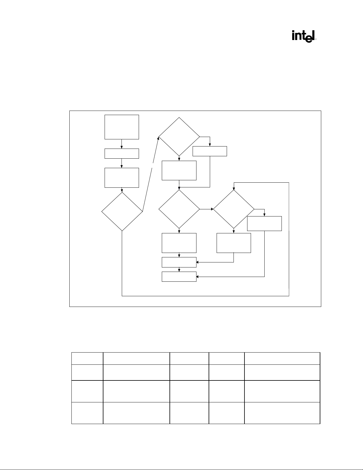
Intel® 82801AA (ICH) & Intel® 82801AB (ICH0) I/O Controller Hub AC ’97
5.3. Codec/Functionality Detection Algorithm
The following flow diagram lists the steps required to detect the codec configuration attached to the
AC_link.
Figure 13. Codec Detection Algorithm
Assign temporary
I/O BARs to Audio
and Modem
functions
(1)
Audio Codec?
(6)
No
R
Remove
AC_RESET#
Wait 400us for
Code Ready status
SDATA_IN_0 Codec
Ready?
(2)
Yes
Read VID's and
(3)
(4)
(5)
write to Func. 5
Modem?
Read VID's and
Write Func. 6
Assert
AC_RESET#
DONE
Yes
Yes
!
Clear BAR, Hide
Function 5
(8)
(9)
No
SDATA_IN_1 Codec
(10)
(11)
(15)
(7)
Ready?
Yes
Read Sec. VID's
and Write Func. 6
(12)
No
Assert AC_RESET#,
Clear BARHide
Function 6
(14)
codec_det_algor
(13)
1. BIOS assigns a temporary I/O address to the BARs for PCI device 31, functions 5 and 6 audio and
modem devices, and enables I/O decoding in the command register, as follows:
Table 16. Initializing the Audio I/O Space (Device 31, Function 5 Audio)
Offset Register Default Initialize Comments
04h–05h Command (COM) 0000h 0005h Bit 2: Bus Master E nabl e
Bit 0: I/O Space Enabl e
10h–13h Native Audio Mixer Base
Address
00000001h 0000XX01h Address in the 64-KB I/O
space. 256 bytes of registers
not in conflict with any other set
14h–17h Native Audio B us
Mastering Base Address
00000001h 0000YY01h Address in the 64-KB I/O
space. 64 bytes of registers not
in conflict with any other s et
40 Programmer’s Reference Manual

Intel® 82801AA (ICH) & Intel® 82801AB (ICH0) I/O Controller Hub AC ’97
R
Table 17. Initializing the Modem I/O Space (Device 31 Function 6 Modem)
Offset Register Default Initialize Comments
04h–05h Command (COM) 0000h 0005h Bit 2: Bus Master Enable
10h–13h Modem Mixer Base
Address
14h–17h Modem Bus Mastering
Base Address
00000001h 0000XX01h Address in the 64-KB I/O space.
00000001h 0000YY01h Address in the 64-KB I/O space.
Bit 0: I/O Space Enabl e
256 bytes of registers not i n conflict
with any other set
64 bytes of registers not i n conflict
with any other set
2. The BIOS removes AC_RESET# in the AC link by setting the AC ’97 Cold Reset bit in the Global
Control Register in either bus master I/O space:
Table 18. Removing AC_RESET# (Address = NABMBAR + 2Ch)
Offset Register Default Initialize Comments
2Ch GLOB_CNT
(Global Control Register)
0000h 0002h Bit 1: AC ’ 97 Col d Reset#. Writing a
1 will cause the AC_RESET# to
deassert.
3. Wait 600 ms to allow for codec internal initialization and the return of the Codec Ready signal.
4. Read the status for SDATA_IN_0 codec ready from the Global Status Register in either bus master
I/O space:
Table 19. Reading the Codec Ready Status (Address = NABMBAR + 30h)
Offset Register Default After
Initialized
Comments
30h GLOB_STA
(Global Status Register)
0000h xxxxh Bit 8: C odec Ready (PCR). Reflects
the ready status of codec attached
to SDATA_IN_0.
5. If no codec is ready, then there is no codec attached to SDATA_IN_0. Because audio should be
attached to SDATA_IN_0, there is no audio codec. The BIOS must clear the BARs assigned to the
PCI audio function, hide the same PCI audio function, and then check for SDATA_IN_1 (see Step
12).
Table 20. Hiding the Audio/Modem Functions (Device 31 Function 0)
Offset Register Default Initialize Comment
F2h Hide Function Register 00h 60h Bit 6: when set hides modem
function
Bit 5: when set hides audio
function
Software must be careful to
preserve the value of any other bit
in this register.
Programmer’s Reference Manual 41

Intel® 82801AA (ICH) & Intel® 82801AB (ICH0) I/O Controller Hub AC ’97
6. If a codec is attached to SDATA_IN_0, then BIOS must determine if the codec is an audio codec
(AC). To determine this, the BIOS writes 8000h (the default value) and reads back the Master
Volume register in audio mixer space in the PCI audio function. BIOS should save the original value
in this register and restore it after this operation, in order to prevent issues during a re-initialization
after a power-saving event.
Table 21. Determining the Audio Codec (Address = NAMBAR + 02h)
Offset Register Default After
Initialized
R
Comments
02h Primary Codec Master
Volume
8000h 8000h If a read to this register returns t he
programmed value, it indi cates
that an audio modem is present.
7. If no audio codec function is detected, BIOS must clear the BARs assigned to the PCI audio function
(see Step 1) and hide the same PCI audio function (see Step 5).
8. If the audio function is detected, BIOS reads the Primary Codec AC ’97 vendor IDs in registers 7Ch
and 7Eh. The BIOS uses these values to program the Subsystem Vendor ID and the Subsystem ID in
the PCI configuration space. See Section 5.4, Details of AC’97 ID Space.
Table 22. Reading the Audio Codec Vendor ID (Address = NAMBAR + 7Ch and 7Eh)
Offset Register Default After
7Ch Prima ry Codec Vendor ID1 Vendor
dependent
7Eh Pri mary Codec Vendor ID2 Vendor
dependent
Initialized
Vendor
dependent
Vendor
dependent
A read to this register ret urns two
ASCII characters for the vendor
ID.
A read to this register ret urns one
ASCII character and s eri al number
for the vendor and codec ID.
Comments
Table 23. Programming the PCI Audio Subsystem ID (Device 31 Function 5)
Offset Register Default Initialize Comment
2Ch–2Dh Subsystem Vendor ID 00h Vendor
dependent
2Eh–2Fh Subsystem ID 00h Vendor
dependent
This register should be initi al i zed
with the manufacturer-spec i f i c PCI
SIG ID. This register is one-time
programmable after a system
reset.
This register should be initi al i zed
with codec-specific i nformation.
This register is one-time
programmable after a system
reset.
9. It also is necessary to determine the presence of a modem function in the SDATA_IN_0 codec. This
indicates the presence of a modem codec (MC) or an audio/modem codec (AMC) (depending on the
previous determination of audio presence.) To determine whether a modem function is present,
BIOS reads the Extended Modem Register in the modem function I/O space and verifies that D15
and D14 (ID1, ID0) are clear 0 value and D0 (LIN1) is set to 1.
42 Programmer’s Reference Manual

Intel® 82801AA (ICH) & Intel® 82801AB (ICH0) I/O Controller Hub AC ’97
R
Table 24. Determining the Presence of a Modem Function (Primary Codec)
(Address = MMBAR + 3Ch)
Offset Register Default After
initialized
Comments
3Ch Prima ry Codec Vendor ID1 Vendor
dependent
Vendor
dependent
If D1 and D0 are both 00 and
DO = 1, there is a modem f unction
in the primary codec.
10. If the modem function is detected, BIOS reads the Primary codec AC ’97 vendor IDs in registers
7Ch and 7Eh. BIOS uses these values to program the subsystem vendor ID and the subsystem ID in
the PCI configuration space. These AC ’97 VID registers have the same offset for the primary codec,
regardless of audio or modem function. (See Section 5.4, Details of AC’97 ID Space) Or, the OEM-
selected serial information for the motherboard/riser SKU is used in order to uniquely identify the
driver.
11. Assert AC_RESET#. See Step 2 for the AC_RESET# register information.
12. Read the status of SDATA_IN_1 codec ready from the Global Status Register in either bus master
I/O space:
Table 25. Determining the Presence of a Secondary Codec (Address = NABMBAR + 2Ch)
Offset Register Default After
30h GLOB_STA
(Global Status Register)
0000h xxxxh Bit 9: Codec Ready (SCR).
Initialized
Reflects the status and presence
of the codec attached to
SDATA_IN_1.
Comments
13. If no codec is detected in SDATA_IN_1, BIOS must generate an AC_RESET# (see Step 2), clear the
BARs assigned to the PCI modem function (se e Step 1), and hide the same PCI modem function (see
Step 5).
14. If the codec is present in SDATA_IN_1, BIOS reads the secondary codec AC ’97 vendor IDs in
registers FCh and FEh. BIOS uses these values to program the subsystem vendor ID and the
subsystem ID in the PCI configuration space. (See Section 5.4, Details of AC’97 ID Space) Or, it
uses the OEM-selected serial information for the motherboard/riser SKU in order to uniquely
identify the driver.
Table 26. Reading the Secondary Modem Codec Vendor ID (Address = MMBAR + FCh and FEh)
Offset Register Default After
FCh Secondary Codec Vendor
ID1
FEh Secondary Codec Vendor
ID2
Vendor
dependent
Vendor
dependent
Initialized
Vendor
dependent
Vendor
dependent
A read to this register ret urns two
ASCII characters for the vendor
ID.
A read to this register ret urns one
ASCII character and the serial
number for the vendor and codec
ID.
Comments
Programmer’s Reference Manual 43

Intel® 82801AA (ICH) & Intel® 82801AB (ICH0) I/O Controller Hub AC ’97
Table 27. Programming the PCI Modem Subsystem ID (Secondary Codec) (Device 31 Function 5/6)
Offset Register Default Initialize Comment
R
2Ch–2Dh Subsystem Vendor ID 00h Vendor
2Eh–2Fh Subsystem ID 00h Vendor
15. This completes the configuration.
5.4. Details of AC ’97 ID Space
The AC ’97 specification allows for two 16-bit sets of vendor-specific IDs.
BIOS should read the codec VID1 and VID2 and use them as references into a lookup table, in order to
determine:
• Subsystem Vendor ID (PCI SIG-assigned number of the codec, AMR or motherboard manufacturer)
• Subsystem ID (AMR and/or codec device ID)
dependent
dependent
This register should be initi al i zed
with the manufacturer-spec i f i c PCI
SIG ID. This register is one-time
programmable after a system
reset.
This register should be initi al i zed
with codec- or OEM/AMR-specific
information. This regi ster is onetime programmabl e after a system
reset.
These registers must be programmed to enable proper device driver enumeration and loading. The entries
in the lookup table vary according to the OEM integration and sourcing requirements. In the audio
function, programming the VID2 value into the subsystem ID could be sufficient for Step 2. However,
for modem riser SKUs, the codec ID is not sufficient and the OEM should provide a unique serialization
of the subsystem ID for the modem riser.
Table 28. Codec Vendor ID Registers
Bits D[15:8]
Reg Name D15 D14 D13 D12 D11 D10 D9 D8 Default
7Ch Vendor ID1 F7 F6 F5 F4 F3 F2 F1 F0 NA
7Eh Vendor ID2 T7 T6 T5 T4 T3 T2 T1 T0 NA
Bits D[7:0]
Reg Name D7D6D5D4D3D2D1D0Default
7Ch Vendor ID1 S7 S6 S5 S4 S3 S2 S1 S0 NA
7Eh Vendor ID2 REV7 REV6 REV5 REV4 REV3 REV2 REV1 REV0 NA
44 Programmer’s Reference Manual

Intel® 82801AA (ICH) & Intel® 82801AB (ICH0) I/O Controller Hub AC ’97
R
5.5. Proposed Mechanism for Accomplishing Modem Riser Enumeration
The following proposal attempts to address the basic PnP requirements for AMR modem
implementations:
5.5.1. Using BIOS Fail-Safe Mode
The essential issue for the OEM and AMR IHV is to provide a unique identification (AMR model no.) of
the motherboard AMR combination. Model information is available for AMR devices from the IHV.
However, this information is not readily available for the BIOS to correctly program the PCI modem
function in the ICH . Given that the AMR is added during the final stages of manufacturing, BIOS does
not have a clear predetermination of which AMR is populated on the motherboard.
A possible solution is to provide a BIOS setup option that is accessible only during manufacturing or
during a fail-safe recovery process. The Setup Option AMR ID allows the manufacturing operator to
enter the unique ID of the AMR module stuffed for the specific motherboard. The ID could easily be
retrieved from the AMR PCB silkscreen or a similar mechanism. This number then would be used by
BIOS during AC ’97 identification and programmed in the Subsystem ID field of the PCI AC ’97
Modem Function.
With the unique ID program in the SSID and the Codec PnP ID providing the information for the
SSVID, the PCI modem function can load a driver that is uniquely identified for the AMR option.
Key Features of the Proposal (i):
• Fail-safe BIOS is available only during manufacturing or by changing a jumper on the motherboard.
• The user cannot accidentally change the AMR ID.
• The AMR is uniquely identified.
• The driver can safely load based on the SSVID and SSID information.
• The OEM requires a manufacturing step change/addition.
• BIOS must add a new setup option.
Programmer’s Reference Manual 45
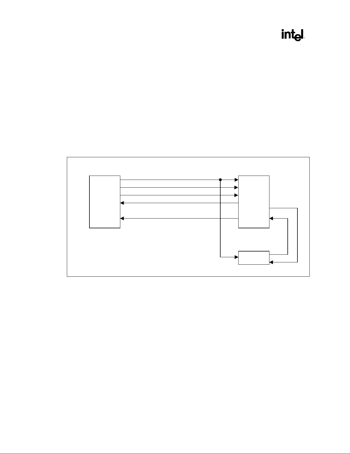
Intel® 82801AA (ICH) & Intel® 82801AB (ICH0) I/O Controller Hub AC ’97
5.5.2. Using the Serial EPROM or Shift Register
At present, the AC ’97 modem codec provides a number of GPIO pins in order to control external logic.
A pair of GPIOs can be used to clock-in a unique ID from an external serial EPROM or shift register.
The clocking procedure could be followed by BIOS during AC ’97 identification and could be
programmed in the SSID register.
With the unique ID program in the SSID and because the codec PnP ID provides the information for the
SSVID, the PCI modem function is capable of loading a driver that is uniquely identified for the AMR
option.
The figure below shows a diagram of this implementation:
Figure 14. EPROM Diagram
Digital AC '97
Controller inside ICH
RESET#
SDATA_OUT
SYNC
BIT_CLK
SDATA_IN_0
AMC/MC'97
Primary
Codec
R
GPOx
GPIy
Key Features of the Proposal (ii):
• The user cannot accidentally change the AMR ID.
• The AMR is uniquely identified.
• The driver can safely load based on the SSVID and SSID information.
• The BIOS must add a new identification algorithm.
• The AMR cost is increased by the added logic.
• Current produced AMRs may not be able to use this methodology.
S-EPROM
Data
Clock
eprom_dia
46 Programmer’s Reference Manual

Intel® 82801AA (ICH) & Intel® 82801AB (ICH0) I/O Controller Hub AC ’97
R
6. Appendix B: Detail for AC ’97 Controller Wake-Up Detection Circuitry
The following diagram illustrates the wake-up detection circuitry for the AC ’97 controller:
Figure 15. Wake-Up Circuitry Representation
SDATA_IN1
SDATA_IN0
Bit_CLK_Present
GPI_STS_CHG (Ring)
AC97_EN
AC97_STS
WAKE
(SCI or SMI)
SDATA_IN[0] : AC ’97 serial data input 0 attached to the primary codec
SDATA_IN[1] : AC ’97 serial data input 1 attached to the secondary codec
Bit_CLK_Present: Represents the presence of AC ’97 bit clock signal.
GPI_STS_CGH: Indicates the codec GPI status change reported in slot 12.
AC ’97_EN: Indicates that the AC ’97 wake-up circuitry has been enabled.
AC ’97_STS: Indicates that the wake-up status was requested.
WAKE: Indicates a system request for a wake-up event. (Translates to SCI or SMI, depending on the
power management procedure.)
The following tables list the possible codec combinations, the possible power states, and how they
resolve for a wake-up event.
Programmer’s Reference Manual 47

Intel® 82801AA (ICH) & Intel® 82801AB (ICH0) I/O Controller Hub AC ’97
Table 29. Wake-Up Condition Table for AC/MC Configuration
Codec
Config.
System
State
Audio
Sleep State
Modem Sleep
State
R
Status Wake on
Audio 1 &
Modem 2
Audio 1 &
Modem 2
Audio 1 &
Modem 2
S0 D0/D2
(link active)
S0 D3
(link
inactive)
S1–S5* D3
(link
inactive)
D3 wake
enabled
D3 wake
enabled
D3 wake
enabled
Bit_CLK = 1
AC97_EN = 1
GPI_STS = 1
Bit_CLK = 0
AC97_EN = 1
GPI_STS = 1
Bit_CLK = 0
AC97_EN = 1
GPI_STS = 1
Table 30. Wake-Up Condition Table for AMC Configuration
System
State
AMC 1 S0 D0/D2
AMC 1 S0 D3
AMC 1 S1–S5* D3
Audio
Sleep State
(link active)
(link
inactive)
(link
inactive)
Modem Sleep
State
D3 wake
enabled
D3 wake
enabled
D3 wake
enabled
Status Wake on
Bit_CLK = 1
AC97_EN = 1
GPI_STS = 1
Bit_CLK = 0
AC97_EN = 1
GPI_STS = 1
Bit_CLK = 0
AC97_EN = 1
GPI_STS = 1
Table 31. Wake-Up Condition Table for Single AC or MC Configuration
System
State
Audio
Sleep State
Modem Sleep
State
Status Issue
OK
(modem SDATA_I N
active)
OK
(modem Ring GPI
active)
OK
(modem Ring GPI
active)
OK
(modem SDATA_I N
active)
OK
(modem ring GPI active)
OK
(modem ring GPI active)
Audio 1 S0–S5 D3
(link
inactive)
Modem 1 S0 N/A D3 wake
Modem 1 S1–S5 N/A D3 wake
N/A Bit_CLK = 0
enabled
enabled
AC97_EN = 0
Bit_CLK = 0
AC97_EN = 1
GPI_STS = 1
Bit_CLK = 1
AC97_EN = 1
GPI_STS = 1
OK
(modem SDATA_I N
active)
OK
(modem ring GPI active)
OK
(modem ring GPI active)
48 Programmer’s Reference Manual

Intel around the world
United States and Canada
Intel Corporation
Robert Noyce Building
2200 Mission College Boulevard
P.O. Box 58119
Santa Clara, CA 95052-8119
USA
Phone: (800) 628-8686
Europe
Intel Corporation (UK) Ltd.
Pipers Way
Swindon
Wiltshire SN3 1RJ
UK
Phone:
England (44) 1793 403 000
Germany (49) 89 99143 0
France (33) 1 4571 7171
Italy (39) 2 575 441
Israel (972) 2 589 7111
Netherlands (31) 10 286 6111
Sweden (46) 8 705 5600
Asia-Pacific
Intel Semiconductor Ltd.
32/F Two Pacific Place
88 Queensway, Central
Hong Kong, SAR
Phone: (852) 2844 4555
Japan
Intel Kabushiki Kaisha
P.O. Box 115 Tsukuba-gakuen
5-6 Tokodai, Tsukuba-shi
Ibaraki-ken 305
Japan
Phone: (81) 298 47 8522
South America
Intel Semicondutores do Brazil
Rue Florida, 1703-2 and CJ22
CEP 04565-001 Sao Paulo-SP
Brazil
Phone: (55) 11 5505 2296
For more information
To learn more about Intel Corporation, visit our site
on the World Wide Web at www.intel.com
 Loading...