

Page 1

Intel 8255x 10/100 Mbps Ethernet Controller Family
Open Source Software Developer Manual
January 2003
Revi sion 1.0
Page 2

Information in this document is provided in connection with Intel® products. This specification, the Intel 8255x 10/100 Mbps Ethernet Controller Family
Open Source Software Developer Manual, is provided “as is” with no warranties whatsoever, including any warranty of merchantability,
noninfringement, fitness for any particular purpose, or any warranty otherwise arising out of any proposal, specification or sample. Intel products are
not intended for use in medical, life saving, life sustaining applications. Intel may make changes to specifications and product descriptions at any time,
without notice.
Intel may make changes to specifications and product descriptions at any time, without notice.
Designers must not rely on the absence or characteristics of any features or instructions marked “reserved” or “undefined.” Intel reserves these for
future definition and shall have no responsibility whatsoever for conflicts or incompatibilities arising from future changes to them.
®
The Intel
from published specifications. Current characterized errata are available on request.
The information in this document is furnished for informational use only, is subject to change without notice, and should not be construed as a
commitment by Intel Corporation. It is intended to enable the maintenance of the open source Intel
adapters. Intel Corporation assumes no responsibility or liability for any errors or inaccuracies that may appear in this document or any software that
may be provided in association with this document. Except as permitted by such license, no part of this document may be reproduced, stored in a
retrieval system, or transmitted in any form or by any means without the express written consent of Intel Corporation.
Contact your local Intel sales office or your distributor to obtain the latest specifications and before placing your product order.
Copies of documents which have an ordering number and are referenced in this document, or other Intel literature may be obtained by calling
1-800-548-4725 or by visiting Intel's website at http://www.intel.com.
Copyright © 2003, Intel Corporation.
* Other product and corporate names may be trademarks of other companies and are used only for explanation and to the owners’ ben efit, without
intent to infringe.
82557, 82558, 82559, 82550, and 82551 may contain design defects or errors known as errata which may cause the product to deviate
®
PRO/100 drivers for the Intel® PRO/100 family of
ii
Intel 8255x 10/ 100 M bps Ethern et Co ntroller Family O pen Sourc e Sof tware Devel ope r Manua l
Page 3

Contents
Contents
1 Introduction....................................................................................................................................1
1.1 Scope....................................................................................................................................1
1.2 Document Conve nt ions ..... ........................ ............................... ............................... .............2
1.2.1 Device References .................................................................................................. 2
1.2.2 Numbering...............................................................................................................2
1.2.3 Signal Name Representation.................................... ............ ....... ....... .......... ....... ....2
1.2.4 Memory Alignment Terminology..............................................................................2
2 Adapter and Controller Overview ................................................................................................5
2.1 Adapter Block Diagram.......................................................... .......... ....... .. ....... .......... .. ....... ..5
2.2 Intel Fast Ethernet MAC Features ........................................................................................6
2.2.1 82557 Features............................................................................................... .........6
2.2.2 82558 Features............................................................................................... .........6
2.2.3 82559 , 82550, 82551, and 82562 Fe atures.. ...........................................................7
2.3 Working with the Physical Layer...........................................................................................7
3 Power Management Interface.......................................................................................................9
3.1 Low Power Mode Requirements...........................................................................................9
3.2 Device Power States............................................................................................................9
3.3 Power Management Registers ................................... .............................. ............................9
3.4 Link Operation ....................................................................................................................10
4 PCI Interface.................................................................................................................................11
4.1 PCI Configuration Space ....................................................................................................11
4.1.1 Vendor ID (Offset 0)...............................................................................................12
4.1.2 Device ID (Offset 2) ...............................................................................................12
4.1.3 Command Register (Offset 4) ................................................................................12
4.1.4 Status Register (Offset 6)......................................................................................12
4.1.5 Revision (Offset 8).................................................................................................13
4.1.6 Class Code (Offset 9) ............................................................................................14
4.1.7 Cache Line Size (Offset C).................................................................................... 14
4.1.8 Latency Timer (O ffset D) .............. ........................ .............................. ...................14
4.1.9 Header Type (Offset E).. ........................................................................................14
4.1.10 Built in Self Test ( Of fset F)............ ........................ .............................. ...................15
4.1.11 Subsystem ID (Offse t 2 C ).................................. ............................... .....................16
4.1.12 Subsystem Vendor ID ( Of fse t 2E) .......... .............................. ........................ .........16
4.1.13 Expansion ROM Base Address Register (Offset 30).............................................16
4.1.14 The Capabilit ies Pointer (Offse t 34)............................. ............................... ...........17
4.1.15 Interrup t Lin e (Offset 3C)................................... ............................... .....................17
4.1.16 Interrup t Pin (Offset 3D)............................................ ............................... ..............17
4.1.17 Max_Lat / Min_Gnt ( O ffset 3E)............................. .............................. ...................18
4.1.18 Power Management PCI Configuration Registers.................................................18
4.2 PCI Command Usage.........................................................................................................21
4.2.1 Memory Write and Invalidate.................................................................................22
4.2.2 Read Align .............................................................................................................23
4.2.3 Odd Byte Alignmen t Support .................................................................................23
Intel 8255x 10/100 Mbps Eth ernet Controller Family Open Source Software Developer Manual
iii
Page 4

Contents
5 EEPROM Interface .......................................................................................................................25
6 Host Software Interface ..............................................................................................................27
6.1 The Shared Memory Architecture....................................................................................... 27
6.2 Initializing the LAN Controller.............................................................................................29
6.2.1 LAN Controller Addressing Format........................................................................29
6.3 Controlling the Device.........................................................................................................31
6.3.1 Control / Status Registers (CSR).......... ....................... ............................... ...........31
6.3.2 System Control Block (SCB)..................................................................................33
6.3.3 PORT Interface......................................................................................................42
6.3.4 EEPROM Control Register....................................................................................45
6.3.5 Management Data Interface Control Register.......................................................49
6.3.6 Receive Byte Count Register................................... ....................... .......................51
6.3.7 Early Receive Interrupt..........................................................................................52
6.3.8 Flow Control Register............................................................................................ 53
6.3.9 Powe r Manage men t Driver Register......................................................................54
6.3.10 General Control Register....................................................... .. ....... ....... .......... ......55
6.3.11 General Status Register ........................................................................ ............ ....56
6.4 Shared Memory Structures............... ............................... ............................... ....................57
6.4.1 Action Commands and Operating Modes......... ................ ............................... ......57
6.4.2 Spe cific Action Comm ands....................................................................................59
6.4.3 Receive Operati o n.......... ................. ........................ .............................. ................97
6.5 Command Unit and Receive Unit Operation.....................................................................103
6.5.1 Starting and Comp leting Control Commands......................................................103
6.5.2 Generating and acknowledging interrupts...........................................................103
6.5.3 Command Unit Control......................... ............................... ....................... .........104
6.5.4 Receive Unit Contro l............... ....................... ............................... .......................106
6.5.5 U pdat ing SCB Status...........................................................................................108
6.6 Flow Control......................................................................................................................108
6.6.1 PHY Based Flow Control ..................................................................................... 109
6.6.2 Frame Based Flow Contr o l................... ............................... .............................. ..109
6.6.3 Priority Aware Frame Based Flow Control...........................................................113
6.6.4 Half Duplex Flow Control.....................................................................................114
6.7 Collision Bac k o f f M od if ic a ti on in Sw i tc he d Environm e nts.......... . .. ... .. .. .. . .... .. . .. .... . .. ..........114
7 Physical Layer Interface ...........................................................................................................115
7.1 Management Data Interface (MDI)...................................................................................115
7.2 MDI Register Set.............. ....................... ............................... ........................ ..................116
7.2.1 Control Registe r : Register 0 ............ ............................... ....................... ..............117
7.2.2 Status Register: Register 1......... ........................ ........................ ....................... ..118
7.2.3 Identificat ion Registers: Registers 2 and 3..........................................................118
7.2.4 Auto-Negotia tion Advertisement Register: Regist e r 4........... ................ ..............119
7.2.5 Auto-Negotia tion Link Partner Abi li ty Register: Regist e r 5..................................120
7.2.6 Auto-Negotiation Expansion Register: Register 6 ...................................... ....... ..120
7.3 Intel 82555 Specific Registers.................................................. ................... ................... ..122
7.3.1 Status and Control Register: Register 16......................... ........................ ...........122
7.3.2 Special Control Register: Register 17..................................................................123
7.3.3 C lock Synthes is Test and Control Register: Register 18 . ....................................124
7.3.4 100B ASE- TX Receive False Carrier Counter: Register 19 .................................124
7.3.5 100Base-TX Receive Disconnect Counter: Register 20......................................124
iv
Intel 8255x 10/ 100 M bps Ethern et Co ntroller Family O pen Sourc e Sof tware Devel ope r Manua l
Page 5

Contents
7.3.6 100BASE-TX Receive Error Frame Counter: Register 21...................................1 25
7.3.7 Receive Symbol Err o r Coun ter: Register 22..................................... ...................125
7.3.8 100BASE-TX Receive EOF Error Counter: Register 23......................................125
7.3.9 10BASE-T Receiv e EOF Erro r Counte r : Register 24......... ........................ .........125
7.3.10 10BA SE-T Transmit Jabber Detect Count er: Register 25 ...................................125
7.3.11 Equali zer Control and Status Register: Register 26 ............................................1 26
7.3.12 Special Control Register: Register 27.................................................................. 1 27
7.4 Auto-Negotiation Functionality..........................................................................................128
7.4.1 Description...........................................................................................................128
7.4.2 Paralle l Dete cti o n..... ............................... .............................. ...............................129
7.5 Vendor-Specific PHY Programming ............................................................................ .....130
7.5.1 Intel 82555 TX PHY.......... ............................... ............................... .....................130
7.5.2 82558 and 82559 Embedded PHY Unit. ..............................................................130
8 Programming Recommendatio ns............................................................................................ 1 33
8.1 Adapter Initialization .........................................................................................................133
8.1.1 8255x Initialization ............................................................................................... 1 33
8.1.2 PHY Detection and Initialization .......................................................................... 1 33
8.1.3 NOS Specific Initialization ....................................................................................1 34
8.2 Transmit Pro ce ssing... ............................... ............................... ............................... .........134
8.3 Frame Reception..............................................................................................................134
8.4 Interrup t Pr o ce ssing......... ........................ ...................................... .............................. ..... 1 35
Appendices
A Wake-up Functiona lit y ..............................................................................................................1 37
B 82550 and 82551 Specific Information.....................................................................................153
Figures
1 8 2 557 Network Interface Car d Blo ck Dia gr a m....................... ........................ ........................ ......5
2 Command Register... ..................................................................................................................12
3 Command Register... ..................................................................................................................13
4 Cache Line Size..........................................................................................................................14
5 Base Address Register for Memory Mapping.............................................................................15
6 Base Address Register for I/O Mapping..................................................................................... 15
7 Expansion ROM Base Address Register............................................ ....... ..... ....... .. .......... .. .......17
8 8 2 55x Memo ry Ar ch itecture......................................... .............................. .................................28
9 SCB Sta tus Word.............. ............................... .............................. ............................... ..............34
10 SCB Command Word........................................ .. ..... ..... ....... .. ..... .. ..... ..... ....... .. ..... .. ..... ....... ... ....36
11 Self-Te s t Res ults Format......... ........................ .............................. ........................ .............. .......43
12 EEPROM Control Register.................... ............................... ........................ ..............................45
13 EEPROM Read Timing Diag ra m................................... ........................ ....................... ..............48
14 General Action Command Format.............................................................................................. 58
15 NOP Command Format..............................................................................................................59
16 Individual Address Setup Command Format..............................................................................60
17 Configure Command Format ......................................................... ..... ....... ....... ..... ....... ..... ....... ..61
18 Multicast Setup Command Format .............................................................................................80
19 Transmit Command Format........................................................................................................81
Intel 8255x 10/100 Mbps Eth ernet Controller Family Open Source Software Developer Manual
v
Page 6

Contents
20 Transmit Buffer Descriptor............ ........................ ........................ ....................... .......................83
21 Load Microcode Comman d Forma t............................................................................................88
22 Dump Command Format............................................. ..... ....... .. ..... .. .......... .. ..... .. ..... ....... ..... .. ....89
23 Diagnose Command Format ............................................................................. ....... ....... ....... ....95
24 Simplified Memory Structure ......................................................................................................98
25 Receive Frame Descriptor Format .............................................................................................98
26 Management Frame Structure...................................................................... ....... ............ ....... ..116
27 Command Block Structu r e... ................ ............................... ............................... .......................144
Tables
1 PCI Configuration Space............................................................................................................11
2 Device and Revision ID..............................................................................................................13
3 Base Ad d re ss Regi ste r Su mmary.......... ........................ ....................... ........................ .............16
4 Power Management Capabilities................................................................................................18
5 Power Man ageme n t Control/Sta tu s Register...................................... ............................... ........20
6 Power Consumption / Dissipation Reporting.................................. ....... ....... ..... ....... .. .......... .. ....21
7 Generated PCI Commands ................................................ ....... ..... ....... ....... ....... ....... .......... ......22
8 Reset Commands..................................................................................................... ....... ...........29
9 Device Addressing Formats.......................................................................................................30
10 Alignment Requirements for 8255x Data Structures ........................ .......... ....... .. ....... ............ ....31
11 Control / Status Register ............................................................................................................ 32
12 System Control Blo ck.................................... ........................ .............................. ............... ........34
13 SCB Status Word Bits Descriptions............................................................................................35
14 SCB Command Word Bits Descriptions ..................................................................................... 37
15 SCB General Pointer for the CU Command............................................................................... 39
16 Statistical Counters. .................................................................................................................... 40
17 Port Register Location................................................................................................................42
18 Port Selection Function ..............................................................................................................43
19 Dump Wake-up Data Struc tu re......... ........................ ....................... ........................ ..................44
20 EEPROM Control Register Locations.........................................................................................45
21 EEPROM Control Register Bits Definitions................................................................................45
22 EEPROM Opcode Summary (64-register EEPROM).................................................................46
23 MDI Control Registe r L o c a ti o n .......... ........................ ....................... ........................ ..................49
24 Management Data Pins...................................................... ....... ....... ..... ....... ....... ....... ................49
25 MDI Control Registe r Bi ts...... ........................ ............................... .............................. ......... .......50
26 Receive Byte Count Register Location.......................................................................................51
27 Early Receive Inte rrupt Register Location..... ........................ .............................. .......................52
28 Flow Control Registers Location.................................................................................................53
29 Flow Control Threshold Values ..................................................................................................54
30 Power Management Driver Register Location ............................................................................54
31 Power Management Driver Register ..........................................................................................55
32 General Contr o l Register Location.... ................. ................ ........................ ........................ ........55
33 General Contr o l Register....... ........................ ........................ ....................... ..............................56
34 General Status Re g ister Location........................... ............................... ........................ .............56
35 General Status Re g ister........ ................. ............................... .............................. .......................56
36 Operation Codes.......................... ............................... ............................... ................................57
37 82557 Configuration Byte Map ............................................................................................. ......62
38 82558 Configuration Byte Map ............................................................................................. ......63
39 82559 Configuration Byte Map ............................................................................................. ......64
vi
Intel 8255x 10/ 100 M bps Ethern et Co ntroller Family O pen Sourc e Sof tware Devel ope r Manua l
Page 7

Contents
40 82557 Dual-Po r t FIFO Settings................ .............................. ............................... .....................65
41 82558 and 82559 Dual-Port FIFO Settings ................................... ............ ....... ....... ............ .......66
42 Extended Statistics Functionality................................................................................................70
43 Pre-amble Length .......................................................................................................................73
44 82558 B-step Configuration Block ARP Frame IP Address.......................... ..............................74
45 82558 B-step ARP Fra me IP Ad d ress Mapping............................... ............................... ...........75
46 Full Duplex Functionality.............................................................................................................77
47 Dump Data Bytes (0-79).............................................................................................................90
48 Dump Data Dwords (20-148)...................................................................................................... 93
49 RFD Status Bit Descriptions.... ........................ ....................... ........................ ............................99
50 Actual Count i n Header RFD.................................. ....................... ........................ ...................100
51 CU Control Commands: Actions at Acceptance Time..............................................................105
52 CU Activities Performed at the End of Execution .....................................................................1 05
53 RU Control Commands: Actions at Acceptance Time..............................................................106
54 Flow Control Frame For m at.......... ....................... ............................... ............................... .......110
55 Flow Control Configuration Bits................................................................................................1 13
56 MDI Register Set...................................................................................................................... 1 16
57 82555 MDI Regist er Set .................................. ....................... ........................ ..........................116
58 24-bit OUI Identification Number ..............................................................................................119
59 MDI Identification Registers 2 and 3: PHY ID Encoding...........................................................119
60 LED Switch Control...................................................................................................................1 28
61 Technology Ability Field Bit Assignments................................................................................. 129
62 Technology Priority...................................................................................................................129
63 Fixed Wake-up Configuration Bits............................................................................................141
64 82559 Port Commands........................................................... ..... ....... ....... ..... ....... .. .......... .. .....148
65 Dump Data Structure................................................................................................................149
66 IPCB Structure..........................................................................................................................153
67 IP Activation Bits (Byte 13)........................... ........................ ............................... ............... ......1 53
68 IP Activation Bits (Byte 12)........................... ........................ ............................... ............... ......1 53
69 IPCB Fields...............................................................................................................................154
70 IPCB Structure Checksum Offload........................................................................................... 1 56
71 IPCB Structu re Lar g e Se nd...................... .............................. ............................... ................... 1 60
Intel 8255x 10/100 Mbps Eth ernet Controller Family Open Source Software Developer Manual
vii
Page 8

Contents
Revision History
Date Revision Description
January 2003 1.0 Initial rele ase.
viii
Intel 8255x 10/ 100 M bps Ethern et Co ntroller Family O pen Sourc e Sof tware Devel ope r Manua l
Page 9

Introduction
This document is intended for use as a software tec hnic al reference manual for the Intel® 10/100
Mbps Fast Ethe rnet controll er family, which includes the 825 57, 82558, 82559, 82550, and 82551,
as well as the 82562 Platform LAN Connect device. It also contains inform ation for several PCI
LAN adapters based on these devices: Intel
PRO/100B Wake on LAN (WOL), Intel
PRO/10+.
1.1 Scope
®
EtherExpress™ PRO/100+, Intel® EtherExpress™
®
EtherExpress™ PRO/100B, and Intel® EtherExpress™
1
This manual is intended to be used as a technical reference for software and test engine ers
developing device dr ivers or related softwa re for adapters or systems using the Intel
82558, 82559, 82550, or 82551 Fast Ethernet controllers or the Intel
Connect (PLC) device. It contains reference information about the controllers as well as other
information th at may be required by software developers (such as PHY information, EEPROM
contents, PCI scanning, etc.). Since this document uses many examples and contains sample code
fragments, it is assum ed that the reader has a fundamental und ers tanding of device driver
programming and a working knowledge of both C programming language and x86 assembler
programming language. Familiarity with at least one industry sta ndard network operating system
(NOS) device driver interface (for example, Net work Drive r Interface Specification [NDIS] or
ODI) is also helpful.
®
The Intel
successive order.
Device Notes
82557 First generation Intel® 10/100 Mbps Fast Ethernet Controller (includes MAC unit only)
82558
82559 Third generation Intel® 10/100 Mbps Fast Ethernet Control ler (inc ludes both a MAC and PHY unit)
82550 Intel® 10/100 Mbps Fast Ethernet Controller (includes both MAC and PHY)
82551 Intel® 10/100 Mbps Fast Ethernet Controller (includes both MAC and PHY)
In general, the Intel family of Fast Ethernet controllers are similar. All family members share the
same core hardware and software interface . The later generation components have a higher
integration and include suppor t for mi scellaneous fea tures (for example, manageability). Since the
differe nt generations of Fast Et hernet controllers are highly simila r, this manu al doc uments the
functionali ty of all de vic es and deta il s the dif f erenc es betwee n the devi ces. It is int ended t o be used
as a tool to maintain and develop software for all devi ces in the Intel family of Fast Ethe rnet
controllers.
10/100 Mbps Fast Ethern et Controller Family includes the following devices in
Second generation Intel® 10/100 Mbps Fast Ether net Controller (include s MAC and an integrated
PHY unit)
®
82562 Platform LAN
®
82557,
Intel 8255x 10/100 Mbps Eth ernet Controller Family Open Source Software Developer Manual
1
Page 10

Introduction
1.2 Document Conventions
1.2.1 Device Refer ences
This do cu m e n t en comp ass e s in f o r mat ion for al l m e m b er s o f th e Intel Fast Eth er n et co ntroll er s:
82551, 82550, 82559, 82558, 82557 and the 82562.
The document convent ion, “8255x,” will be used to refe r to all devices. In addition, there are
specific references to the 82557 throughout this manual that pertains to all 8255x devic es . Devicespecific differences and exceptions will be documented.
1.2.2 Numbering
Decimal, binary, and hexadecimal numbers are used through the manual. They will be de signated
as follows:
• Decimal numbers: Decimal numbers will not be followed by a suffix.
• Binary numbers: Binary numbers (base 2) will be followed by a “b” (for example, 01b).
• Hexadecimal numbers: Hexadecimal numbers (base 16) will be followed with the suffix “h”
(for example, 1Ch). Hexadecimal numbers may also be noted with a pre f ix of “0x” (for
example, 0x1c).
1.2.3 Signal Name Representation
Signals that are active in a low logic state when asserted are followed by the pound sign (#). For
example, FRAME# is asserted low by the master during a transaction. It is asserted low at the start
and duration of a trans action and de-asserted during the final data phase.
Signals that are not followed by a pound sign are ac tive in a high logic state when as serted. For
example, the IDSEL signal is asserted high when the 82559 during PCI read and write transactions.
1.2.4 Memory A lignment Terminology
The 8255x data structures have special memory alignment requirements. T his implies that the
starting phy si cal address of a data structure must be aligned as specified. The following terms are
used for this purpos e:
• Byte alignment: Byte alignment implies that the physical addresses can be odd or even.
Examples: 0FECBD9A1h or 02345ADC6h
• Word ali gnm ent : Word alignment implies that phys ical addresses must be aligned on even
boundaries . In other words, the last nibble of the address may only end in 0h, 2h, 4h, 6h, 8h,
Ah, Ch, or Eh.
Example: 0FECBD9A2h
• Dword alignment: Dword alignment im plies that the physical addres ses may only be aligned
on 4-byte boundarie s. In othe r words, the last nibbl e of the addres s may only end in 0h, 4h, 8h,
or Ch.
Example: 0FECBD9A8h
2
Intel 8255x 10/ 100 M bps Ethern et Co ntroller Family O pen Sourc e Sof tware Devel ope r Manua l
Page 11

Introduction
• Paragraph alignment: Paragraph align me nt implies that the phys ical addresses may only be
aligned on 16-byte boundaries. In other words, the last nibble must be a 0.
Example: 02345ADC0h
Intel 8255x 10/100 Mbps Eth ernet Controller Family Open Source Software Developer Manual
3
Page 12

Introduction
4
Intel 8255x 10/ 100 M bps Ethern et Co ntroller Family O pen Sourc e Sof tware Devel ope r Manua l
Page 13
Adapter and Controller Overview
Adapters based on an Inte l® 8255x device support the ANSI/IEEE 802.3u standard for 100BASETX (100 Mbps operation) and 10BASE-T (10 Mbps operation).
2.1 Adapter Block Diagram
The main components of I ntel Fast Ethernet adapters are:
• A Fast Ethernet Media Acces s Controller (MAC), such as the 8255x, is the core component.
The MAC supports the Fast Ethernet ANSI/IEEE 802.3u standard.
• A Physical Layer (PHY) inte rfac e device is also required. The 82558, 82559, 82550, and
82551 components ha ve an i ntegrated PHY that supports 100BAS E-TX and 10BASE-T.
Adapters based on the 82557 must include an appropriate PHY component for their design.
• A serial EE PROM is required to hold the adapter’s individual E thernet node address and othe r
configuration information including fixed PCI configuration parameters.
The adapters are based on 100BASE-T X spe cifications. 100BAS E-TX is a specific scheme
designed for use over 2 pairs of Category 5 unshiel ded twisted-pair cable . 100BASE-TX defines a
signaling sche m e for 100 Mbps and provides compatibi lity with the existing 10 Mbps IEEE 802.3
10BASE-T signaling standard. Since only 2-wire pairs are used, TX technology allows full duplex
operation at 100 Mbps. The Intel 82555 is one possible TX solution.
2
®
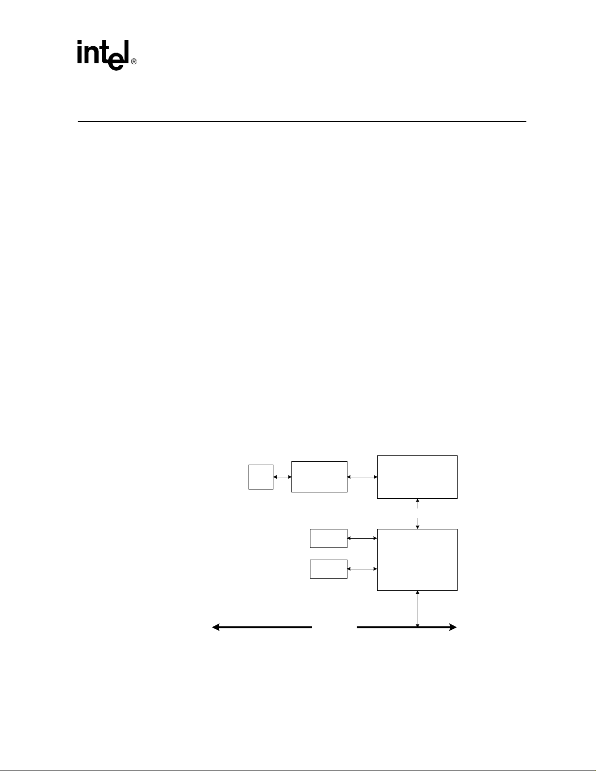
The block diagra m belo w illus trate s an Intel
MAC with a TX or T4 PH Y.
Figure 1. 82557 Network Interface Card Block Diagram
RJ-45
PRO/100B adapter confi gurat ion bas ed on t he 82557
Filter
Module
Optional
Flash
EEPROM
PCI Local Bus
100BASE-T4 or
100BASE-TX PHY
MII
Intel® 82557
Intel 8255x 10/100 Mbps Eth ernet Controller Family Open Source Software Developer Manual
5
Page 14

Adapter and Controller Overview
2.2 Intel Fast Ethernet MAC Features
2.2.1 82557 Features
• Glueless 32-bit, zero wait state PCI bus master interface compliant with PCI Specification,
Revision 2.1.
• 10 and 100 Mbps support in compliance with IEEE 802.3 10BASE-T and 802.3u 100BASE-
TX.
• Fast back-to-back transmit interf rame spacing (IFS) of 960 ns in 100 Mbps networks and 9. 6
µs in 10 Mbps networks.
• On-chip Control/Status Register (CSR) incorporating the System Control Block (SCB).
• Simple and flexible packet support with Dynamic transmit chaining.
• Packed Transmit Buf f er Descriptors (TBDs).
• Early transmit complete indication.
• Simple receive pack et support al lows ear ly receive in terrupt support for concurre nt processing
(in simplified mode).
• IEEE Media Independent Interfac e (MII) compliant PHY interface other MII compliant PHYs.
• Full and half duplex transmit and receive capability.
• Separate on-c hip receive and transmit FI F Os.
• On-chip network management counters.
• EEPROM support.
• Optional Flash ROM support (256 Kbytes or 1 Mbyte).
2.2.2 82558 Features
For the most part, the 82558 is a superset of the 82557. In addi tion to incorporat ing the features of
the 82557, it al so i ncludes the following :
• Backward compatibl e to 82557 software.
• Integrated 100BASE-TX PHY.
• IEEE 802.3u auto-ne gotiation support in 10BASE-T, 100BASE-TX, full dupl ex a nd f ull
duplex flow control configurations.
• Auto-polarity correction for 10BASE-T.
• Optimized PCI interface with support for the memory write and invalida te PCI command.
• Automatic read of EEPROM (programmable I D).
• IEEE 802.3x flow control capable.
• PHY based flow control supp ort when the internal 100BASE-TX PHY is used.
• Advanced Configuration and Power Interface (ACPI) Specification and PCI Power
Management Specification compliant.
• Remote power up support (for Magic Packet*).
6
Intel 8255x 10/ 100 M bps Ethern et Co ntroller Family O pen Sourc e Sof tware Devel ope r Manua l
Page 15

Adapter and Controller Overview
• Optional Flash support up to 64 Kbytes. (The 82557 is cap able of larger Flash size support.)
2.2.3 82559, 82550, 82551, and 82562 Fea tures
The 82559, 82550, and 82551 devices are supersets of the 82557 and 82558. However , the 82559
does not support PHY based flow control as the 82558 did. The new 82559 features are:
• Backward compatible to the 82557 and 82558 software.
• Low power 3.3 V device:
• Clockrun protocol support.
• System Management Bus (SMB) s upport.
• Wired for Management support (WfM).
• Expanded Wake on LAN capabiliti es .
• 128 Kbytes Flash size support. (The 82558 only supp orted a 64 Kbyte Flash.)
• Thin ball grid array (BGA) 15 x 15 mm package.
2.2.3.1 82559ER Features
The 82559ER is a member of the 82559 Fast Eth ernet controllers. It is a subset of the 82559.
However, the 82559ER does not support:
• SMB.
• Wake on Magic Packet*.
2.3 Working with the Physical Layer
The 82557 contains an IEEE MII compl iant interface to a MII complian t P HY, allowing
connections to 10/100 Mbps networks. Software communicates to a MII compl iant device thro ugh
the 82557 by using the its Management Data Interface (MDI) port.
The 82558, 82559, 82550 and 82551 contain an embedded PHY module. Although the PHY is
internal for these devices, software still communicates to the PHY unit through the MDI port.
For 10/100 Mbps connections, t he 82557 can be used in conjunction with the Intel
Mbps only connections, the 82557 can be interfaced to the Intel
maintaining software compatibil ity to 100 Mbps solutions. The 82558 and later devices do not
have a 10 Mbps only interface as the 82557. However , it is possible to interface these devices with
a 10 Mbps only MII device.
®
®
82503 serial interface, while
82555. For 10
Intel 8255x 10/100 Mbps Eth ernet Controller Family Open Source Software Developer Manual
7
Page 16

Adapter and Controller Overview
8
Intel 8255x 10/ 100 M bps Ethern et Co ntroller Family O pen Sourc e Sof tware Devel ope r Manua l
Page 17

Power Management Interface
The 82557 has no power management support. The 82558 added support for th e Advanced
Configuration and Power Interface (ACPI) Specification and limited support for Wake on LAN
(WOL). The 82558 B-s tep upgraded and expanded the WOL capability, while the 82559 expanded
and simplified the WOL functionality even more.
3.1 Low Power Mode Requirements
The 82558, 82559, 825 50, a nd 82551 adhere to the emerging power management sta ndards as
defined in:
• PCI Bus Power Management Interfa ce Specificatio n, Revision 1.0.
• Advanced Configura tion and Power Interface Specification (ACPI), Rev 1.0; Dec ember 22,
1996.
• Device Class Power Managem ent Reference Specification - Network Device Class, Revision
1.0.
These three specifications define how a PCI network device can be controlled in an OS Directed
Power Management (OSPM) environment. These devices all adhere to these specific ations.
Additionally, they support bus isolation within the chip and Wake on LAN (WOL) capabilities.
3
3.2 Device Power States
Currently, operating systems only support the D0 and D3 power states. However, starting with the
82558, the Intel Fast Ethernet controller fami ly supports all four power states as defined in the PCI
Power Management Specification. These power states are named D0, D1, D2 and D3. D0 is the
maximum powered state, and D3, the minimum powered state.
3.3 Power Management Re gis ters
The 82558, 82559, 82550, and 82551 support power manage ment registers:
• Power Management Capability Pointer (Cap_Ptr)
• Power Management Capabilities (PMC)
• Power Management Control/Status Register (PMCSR)
• Power Management Driver Register (PMDR)
The first three registers are located in PCI configuration space and are defined in the PCI Power
Management Spec ification. It is part of the device CSR, which is mapped into sys tem memory and
I/O space.
Intel 8255x 10/100 Mbps Eth ernet Controller Family Open Source Software Developer Manual
9
Page 18

Power Management Interface
3.4 Link Operation
In the D0 state, the device maintains an active link. The 82558 B-step (refer to Table 2, “Device
and Revisi on ID” on page 13) and later devices also maintain an active link in the D3 state if PME
is enabled and the device has power. This implies:
• 10BASE-T Mode: The device expects a normal clock input on the X1 a nd X2 pins. It expects
to receive norma l reception on the Rece iv e Differ ential Pos itive and Receive Differential
Negative signals (RDP/RDN pair). The device will not transmit on the Transmit Dif f erential
Positive and Tra n smit Diffe r ential Negative signal s (TDP/TDN pair).
• 100BASE-TX Mod e: The device expects a normal cloc k input on the X1 and X2 pins and to
receive normal reception on the RDP/RDN pair. It transmits a continuous idle st ream on the
TDP/TDN pair, as required by the 100BASE -TX s tandard. The 82558 does not transmit
frames on the link.
• Auto-Negotiation: If the link f ails whil e th e device is in the D1 state, it performs the nor mal
auto-negoti ation p roto col in or der t o re-est abl ish t he link. F or the 8 2558 B -step , if the link fa il s
in the D3 state and PME is enabl ed and t he devi ce has power , th e devic e will attempt to use the
normal auto-negotiation protocol in order to re-establish the link. If the link fails on the 82559
in the D3 state and PME is enabled and the device has power, the 82559 will go into a deep
power down state, rather than trying to re-establish the link with the auto-ne gotiation prot ocol.
During the D3 power state, the 82558 A-step does not mainta in an active link. The 82558 B-st ep
and later generation devices do not maintain a link in D3 if PME is disabled or if the device does
not have power.
10
Intel 8255x 10/ 100 M bps Ethern et Co ntroller Family O pen Sourc e Sof tware Devel ope r Manua l
Page 19

PCI Interface
4.1 PCI Configuration Space
One of the most important functions for enabling superior configurability and ease of use is the
ability to r elocate PCI devices in the address spaces. By def ault PCI devices support “Plug and
Play.” When the system is powered on, dev ice independent software (usually the system BIOS)
determines present devices, builds an address map, and assigns non-conflicting resources to those
devices. The device independent software accomplishes this configuration task by writing to the
PCI configuration s pace of each individual PCI dev ice.
The 8255x supports 16 Dwords of Type 0 Configuration Space Header, as defined in the PCI
Specification, Revision 2.1. The 82259 and 82558 also support a small section in the device
specific configuration space. The configuration space is depicted below. The registers that are not
identi cal betw ee n the de vi ce s ar e s h ad e d.
Table 1. PCI Configuration Space
4
Byte Offset
(hexadecimal)
0
4
8 Class Code (200000h)
CBIST
10 CSR Memory Mapped Base Address Register
14 CSR I/O Mapped Base Address Regist er
18
1C
20
24
28
2C
30
34 Reserved
38 Reserved
3C Max_Lat ency (FFh) Min_Grant (FF h) Interrupt Pin (01h) Interr upt Line
DC
E0
Byte 3 Byte 2 Byte 1 Byte 0
Device ID Vendor ID
Status Register Command Register
Header Ty pe Latenc y Timer C a che Line Siz e
Flash Memory Mapped Base Address Regis ter
Reserved
Subsystem ID Subsystem Vendor ID
Expansion ROM Base Address Register
Power Management Capabilities Next Item Pointer Capability ID
Reserved Data Power Management CSR
Revision ID
Cap_Ptr
Intel 8255x 10/100 Mbps Eth ernet Controller Family Open Source Software Developer Manual
11
Page 20

PCI In terfac e
4.1.1 Vendor ID (Offset 0)
This field ide ntifies the device manufacturer. For the 82557 B-ste p this field equals 8086h. For the
82557 C-Ste p, 82558, and 82559, this fie ld i s automa tical ly loade d from the EEPROM at power on
or upon the asserti on of PCI reset. If the EEPROM is not present or inva lid, this value defaults to
8086h.
4.1.2 Device ID (Offset 2)
This field uniquely identifies the devi ce . For the 82557 B-step this field i s 1229h. For the 82557 CStep, 82558, and 82559, this field is automatically loaded from the EEPROM at power on or upon
the asse rtion of PCI reset. If the EEPROM is not present or invalid, this value defaults to 12 29h for
the 82558 and 82559. The 82559ER does not load the Device ID from the EEPROM and will
always equal 1209h.
4.1.3 Command Register (Offset 4)
The Command Register provides control over the device’s ability to generate and respond to CPU
cycles. Its layout is shown below. The shaded bits are not used and are hard-wired to 0.
Figure 2. Comm a n d R egi s te r
15 10 9 0
Reserved Command Bits
Bits
15:10 0 Reserved.
9 0 Fast back-to-back enable.
8 x SERR# enable.
7 0 Wait cycle enable.
6 x Parity error response
5 0 Palette snoop enable.
4x
3 0 Special cycle monitoring.
2 x Ma stering enable.
1 x Memory access enable.
0 x I/O acce s s en ab le .
Initial
Value
Memory write and invalidate (MWI) enable.
NOTE: More information regarding the MWI command is loca ted in Section 4.2.1,
Description
“Memory Writ e and Invalidate”.
4.1.4 Status Register (Offset 6)
The Status Register is used to record status information for PCI bus related events. Its layout is
shown below. The shaded bits are not used and are hard-wired to 0.
12
Intel 8255x 10/ 100 M bps Ethern et Co ntroller Family O pen Sourc e Sof tware Devel ope r Manua l
Page 21

Figure 3. Command Registe r
15 43 0
Status Bits Reserved
PCI Interface
Bits
15 x Detected parity error.
14 x Signaled system error.
13 x Received master abort.
12 x Recei ved targ et abort.
11 0 Signaled target abort.
10:9 01 DEVSEL timing (indicates minimum timing).
8 x Data parity reported.
7 1 Fast ba ck-to-back capabl e.
6 0 UDF supported.
5 0 66 MHz capable.
4
3:0 0 Reserved.
Initial
Value
1 (82559
and
82558)
0
(82557)
Capabilities list. This bit indicates whether the device implements a list of new capabilities
such as PCI Power Management. If it is set, the Cap_Ptr register in the PCI Configuration
Space points to the location of the first item in the Capabilities List.
NOTE: This bi t is set to 1 f or the 82559 an d 82558 if it i s not disabled by the EE PROM. I t
is always equal to 0 for the 82557.
4.1.5 Revision (Offset 8)
This register specifies a device specific revision identifier. For the 82557 C-Step, 82558, and
82559, this f ield m ay be a utoma tical ly loa ded f rom the EEPROM at power on or u pon th e asserti on
of a PCI reset. The default revision register values for the various devices are:
Description
Table 2. Device and Revision ID
Device Revision ID
82557 A-Step 01h 2.0 Yes
82557 B-Step 02h 2.0 Yes
82557 C-Step 03h 2.1 No
82558 A-Step 04h 2.1 Yes
82558 B-Step 05h 2.1 Yes
82559 A-Step 06h 2.1 No
82559 B-Step 07h 2.1 No
82559 C-Step 08h 2.2 Yes
PCI Revision
Supported
Intel 8255x 10/100 Mbps Eth ernet Controller Family Open Source Software Developer Manual
Intel Driver
Supported
13
Page 22

PCI In terfac e
Table 2. Device and Revision ID
Device Revision ID
82559ER A-Step 09h 2.2 Yes
82550 0Ch, 0Dh, 0Eh 2.2 Yes
82551 0Fh, 10h 2.2 Yes
4.1.6 Class Code (Offset 9)
The class code, 020000h, identifies the device as an Ethernet adapter.
4.1.7 Cache Line Size (Offset C)
This regis ter specifie s the system cache line size in units of 32-bit words and ca n be read or written
to. The system BIOS or OS should initialize this register at power on or after a PCI reset .
The 82557 does no t suppor t Me mory W rit e and In valida te (MWI) and the refore re turns 0 when thi s
register is re ad. The 82258 and 82559 support the MW I command and must support this register.
The 82558 and 82559 can only support cache line sizes of 8 and 16 Dwords. Any value other than
8 or 16 written to the register is ignored, and the dev ice does not use the MWI command. If a value
other than 8 or 16 is written into the Cache Line Size (CLS) register, the device returns all zero es
when th e CL S re gi ster is rea d.
Figure 4. Cache Line Size
PCI Revision
Supported
Intel Driver
Supported
76543210
0 0 0 RWRW0 0 0
Bit 3 is set to 1 only if t he value 00001000b (8) is written to this register. Bit 4 is set to 1 only if the
value 00010000b (16) is written to this register. All other bits are read only and will return 0 on
read.
4.1.8 Latency Timer (Offset D)
This register sp ecifies, in units of PCI bus clocks, the minimum time that a bus master can retain
ownership of the bus. This value is set by the PCI bus arbitrator based on the values in the
maximum latenc y ( Max_Lat) and Maximum Grant (Max_Gnt) regis ters.
4.1.9 Header Type (Offset E)
This byte fi el d ident if i es the lay o ut of the seco n d part of the p red efi n ed con figu r at ion spa c e head er
and if the device is a multi-function compone nt. The 82557 and 82558 are both single function
devices and have this register hard-coded to 00h. For the 82559, the value of this register is
determined by a bit in the EEPROM. This register should read 00h for a standard Ethernet adapter,
00h.
14
Intel 8255x 10/ 100 M bps Ethern et Co ntroller Family O pen Sourc e Sof tware Devel ope r Manua l
Page 23

4.1.10 Built in Self Test (Offset F)
This optional register is used for control and status of Built in Self Test (BIST). This register is
hard-wired to 0 indicating that the dev ices do not support BIST.
Three base address registers are supported by the 8255x:
• CSR Memory Mapped Base Address Register (BAR 0 at offset 10)
• CSR I/O Mapped Base Address Register (BAR 1 at offset 14)
• Flash Memory Mapped Base Address Register (BAR 2 at offset 18)
Two request memory mapped resources, and the third, I/O mapping. Each register is 32 bits wide.
The least significant bit in each base add ress register determines w hether it represen ts an I/O or
memory space. The figures below illustrate layouts for I/O and memory mapped base address
registers. After determining which resources wil l be used, the power-up software maps the I/O and
memory controller s into available locations and continues wit h the power up. To perform the
mapping in a device independent manner, the base registers are placed in the pr edefined header
portion of confi guration space. Device drivers access th is configuration space to determine the
mapping of a particul ar device.
Figure 5. Base Address Register for Memory Mapp ing
PCI Interface
32 43 0
Base Address Configuration Bits
Bits
31:4 x Base Address.
3 x Pre-fetchable.
2:1 x
0 0 Memory space indicator.
NOTE: Bit 0 in all base registers is read-only and used to determine whether the register maps into memory or
Initial
Value
00 = Locate address anywher e in 32-bi t address s pace.
01 = Locate address below 1 MByte.
10 = Locate address anywher e in 64-bi t address s pace.
11 = Reserved.
I/O sp ace. Base registers mapping to memory space must return a 0 in bit 0, and base registers
mappin g to I/O space, a 1.
Figure 6. Base Address Register for I/O Mapping
32 21 0
Base Address Reserved 1
NOTE: Base registers that map into I/O space are always 32 bits with bit 0 hard wired to a 1, bit 1 is reserved
and must return 0 on reads, and the other bits are used to map the device into I /O space.
Description
The number of upper bits that a device actually implements depends on how much of the address
space the device responds to. A device that wants a 1 Mbyte memory address space would set the
most significant 12 bits of the base address register to be configu r able, setting the other bits to 0.
Intel 8255x 10/100 Mbps Eth ernet Controller Family Open Source Software Developer Manual
15
Page 24

PCI In terfac e
The 8255x requires one BAR for I/O mapping and one BAR for memory mapping of these
registers anywhere within the 32-bi t memory address space. The driver determines which BAR (I/
O or Memory) is used to access the Control/Sta tus Registers. However, both are always requested
by the device.
One BAR is also require d to map the ac ces ses to a n option al Fl ash mem ory. The 82557 implements
this registe r regardless of the presence or absence of a Flash chip on the adapte r. The 82558 and
82559 only imple me nt this register if a bit is set in the EEPROM. The size of the spa ce requested
by this register is 1Mbyte, and it is always ma pped anywhere in the 32-bit memory address space.
Note: Although the 82558 only supports up to 64 Kbytes of Flash memo ry and the 82559 only supports
128 Kbytes of Flash memory, 1 Mbyte of address space is still requested. Software should not
access Flash addresses above 64 Kbytes for the 82558 or 128 Kbyt es for the 82559 because Flash
accesse s abo v e the limit s ar e al iased to lo w e r add r es s es. Table 3 describes the implementation of
the base address register s.
Table 3. Base Address Register Summary
Register
Location
10h
14h I/O space for the device Control/Status Registers. The size of this space is 32 bytes.
18h
1Ch - 27h Reserved.
Description
Memory space for the device Control/Status Registers. The size of this space is 4 Kbytes
and it is mapped anyw here in the 32-bi t memory add ress space. It is marked as prefetchable. Software should not assume that this memo ry will be granted below 1 Mby te.
Memory space for FLASH buffer accesses. The size of this space is 1Mbyte. It is mapped
anywhere in the 32-bit address space and is not pre-f etchable.
4.1.11 Subsystem ID (Offset 2C)
This register uniquely identifies the add-in adapter or subs ys tem where the PCI device resides. It
provides a mechanism to distinguis h different adapters that use the same PCI controller. For the
82557 B-step thi s field equals 0000h. For the 825 57 C-Step and later devices, this field is lo aded
from the EEPROM at power on or upo n the ass ertio n of PCI re set . If the EE PROM is not prese nt or
invalid, this value defaults to 0000h.
4.1.12 Subsystem Vendor ID (Offset 2E)
This register uniquely identifies the add-in adapter or subs ys tem where the PCI device resides. It
provides a mechanism to distinguis h the vendor of a adapter from the vend or of the PCI controller
used on the adapter. For th e 82557 B-step this field is 0000h. For the 82557 C-Step and later
devices, this field is automatically loaded from the EEPROM at power on or upon the as sertion of
PCI reset. If the EEPROM is not present or invalid, this value defaults to 0000h.
4.1.13 Expansion ROM Base Address Register (Offset 30)
The 8255x provides an interface to a local Flash device (or EEPROM) which may be used as an
expansion ROM. A 32-bit E xpansion ROM Base Address Regi st er at offset 30h in the PCI
Configuration Space is defined to handle the address and size information for boot-time access to
16
Intel 8255x 10/ 100 M bps Ethern et Co ntroller Family O pen Sourc e Sof tware Devel ope r Manua l
Page 25

the Flash. The 82557 implements this register regardless of the prese nce or abs ence of a Flash
component on the adapter. For the 82558 and later Fast Etherne t controllers, this register is only
implemen te d if a bit is set in the EEP R O M .
The register func tions exactly lik e a 32-bi t bas e address register exc ept that the encoding ( and
usage) of the bottom bits is different. The upper 21 bits correspon d to the upper 21 bits of the
expansion ROM base address. The 8255x only allow an expansion ROM to be mapped on a 1
Mbyte boundary. Therefore, only the most significant 12 bits are configurable to indicate the 1
Mbyte size requ irement ( as with the Fla sh Memory Ma pped BAR, the 825 58 an d 82559 request a 1
Mbyte mapping even though the maximum Flash size allowed with those devices is 65 Kb ytes).
The format of the register is sh own in the figure below .
Figure 7. Expansion ROM Base Address Register
32 20 19 1 0
Read / Write Reserved (all bits set to 0) En
Bit 0 in the register is used to control whether or not the device accepts accesses to its expansion
ROM. When this bit is reset, the devices expansion ROM address space is disabled. This bit is
programmed at initialization time by the system BIOS. The Memory Space bit in the Command
register has precedence over the Expansion ROM Base Address Enable bit. A device responds to
accesses to its expansion ROM only if both the Memory Space bit and the Expansion ROM Base
Address Enable bit are set to 1 (it is reset to 0 upon PCI reset).
PCI Interface
4.1.14 The Capabilities Pointer (Offset 34)
This an 8-bit field that provides an offse t in the device PCI Configuration S pace for the loca tion of
the first item in the Capabilities Linked List. The Power Management Interface documentation
specifies this linked list to provide access to all appropriate device information in the
implementation of the ACPI.
For the 82257, this register is hard-wire d to 0 si nce it does not support power management.
For the 82558 this r egis ter is set to DCh if powe r mana gement is ena bled in the EEPROM. If power
management is dis abled, then this register is set to 0.
For the 82559 and later Intel Fast Ethernet controllers, this regist er is hard-wired to DCh.
4.1.15 Interrupt Line (Offset 3C)
The Interrupt Line register is an 8-bit register used to communicate interrupt line routing
information. This register is configurable by the system BIOS or OS. POST software writes the
routing information into this register as it initializes and configures the system. The value in this
register specifies which system inte rrupt controller input the device interrupt pin is connected to.
Device drivers and operating systems use this information to determine priority and vector
information.
4.1.16 Interrupt Pin (Offset 3D)
The Interrupt Pin register specifies which interrupt pin the device (or device function) uses. This
register is always set to a 1, indicating that INTA# is used.
Intel 8255x 10/100 Mbps Eth ernet Controller Family Open Source Software Developer Manual
17
Page 26

PCI In terfac e
4.1.17 Max_Lat / Min_Gnt (Offset 3E)
These registe rs specify the device settings for Latency Timer va lues. For both registers , the value
specifies a period of time in units of ¼ microsec ond. Min_Gnt is used to specify the burst length
period the devi ce needs assuming a clock rate of 33 MHz. Max_Lat is used to specify how often
the device needs to gain access to the PCI bus. The value s of these registers are 8h (2 µS) for
Min_Gnt and 18h (6 µS) for Max_Lat.
4.1.18 Pow er Management PCI Configuratio n Registers
4.1.18.1 Capability Identifier (Offset DC)
The Capability Identif ier signals this item in the capability linked list as the PCI Power
Management regis ters. The PCI Power Management registers ha ve be en a ssigned the ID of 01h.
Since power manage ment is not implemented in the 82557, this register is hard-coded to 0 for that
device. For the 82558 and later devices, this rea d only register returns 01h.
4.1.18.2 Next Item Pointer (Offset DD)
The Next Item Pointer register describes the location of the next item in the capability lis t. Since
power managem ent is the last it em in the list, this register is se t to 0.
4.1.18.3 Power Management Capabilities (Offset DE)
The Power Management Capabilities (PMC) register is a 16-bit re ad-only register, which provides
informatio n on the capabilities of the device related to power manage me nt. Since power
management is not imp lemented in the 82557, this register is hard-coded to 0 for that device. For
the 82558 and later devices, this regist er returns values according to the chart below.
T able 4. Power Management Capabilities
Bit Default Value R / W Description
82558A: 00011
82558B, 82559:
31:27
26 1 RO
25 1 RO
24
no auxi liary power
- 01111
with auxiliary
power - 11111
82558A: 1
82558B: 0
82559: 0
RO
RO
PME_Support. This five bit field indicates the power states in
which the device may assert PME#. A value of 0b for any bit
indicates that the function is not capable of asserting the PME#
signa l while in that po w er sta t e.
The 82558 A-step supports wake-up from D0 and D1. The 82558
B-step an d 8255 9 s up po rt w ake- u p fr om D0, D1, D2 a nd D3
auxili ary power is prese nt and from all power state s if auxiliary
power exists.
D2_Support. If this bit is set, this function supports the D2 Power
Managem en t State. All devi ce s mus t sup po rt t he D0 an d D3 s t ates .
The 8255 9 an d later devi ces suppo r t the D 2 P ower Mana ge me nt
State.
D1_Support. If this bit is set, this function supports the D1 Power
Management State. The 82558 and later devices supports the D1
Power Management State.
FullClk. If this bit is set, this function requires a full speed clock at
all times when it is in the D0 state in order to perform its function. If
this bit is cleared, the function only requires a full speed PCI clock
while actually transferring data so dynamic clock control may be
used. The 82558 A-step requires a fu ll speed clock at all times
when it is in the D0 state in order to pe rform its functi on.
hot
if no
18
Intel 8255x 10/ 100 M bps Ethern et Co ntroller Family O pen Sourc e Sof tware Devel ope r Manua l
Page 27

T able 4. Power Management Capabilities
Bit Default Value R / W Description
23 0 RO Reserved. This field is not used by the 8255x.
82558: 0
82559:
22
21 1 RO
20
19 0 RO
81:16 001 RO
no auxiliary power
- 0
with auxiliary
power - 1
82558A: 0
82558B, 82559:
no auxiliary power
- 0
with auxiliary
power - 1
RO
RO
PCI Interface
AUX_Current. If the device is connected to an auxiliary power
supply, the 82559 reports a “1” to indicate that it consume less than
250 mA from the 3.3 Vaux pin while in the D3
reflection of bit 31.
DSI. The Device Specific Initialization bit indicates whether special
initialization of this function is required (beyond the standard PCI
configuration header) before the generic class device driver is able
to use it. Device specific initialization is required for the 82558 and
82559 af ter a D3 to D0 transition.
Auxiliary Power Source
This bit is only meaningful if PM CSR bit 31 (D3
PME) equ als 1 . When t hi s b it al so eq ual s 1, i t indi ca te s th at su ppor t
for PME# in D3
B-step and 82559 require auxiliary power for wake up from the
D3
state. Therefore this bit is set to 1 if auxiliary power is
cold
present.
PME Clock. When this bit is 1, it indicates that the PME#
generat io n l ogi c r equ ir e s it s ho st P CI bu s t o mai n t ain a f ree - run ni ng
PCI clock. When this bit is 0, it indicates that no host bus clock is
required for the functi on to gener ate PME# . The 82558 and later
generation devices do not require a clock to ge nerate PME# and
return 0.
Version. This field specifies to software how to interpret the PMC
and PMCSR registers. A value of 001b indicates that the device
complies with the Revision 1.0 of the PCI Power Management
Interface Specification.
requires an auxiliary pow er supply. The 82558
cold
state. This bit is a
cold
supporting
cold
4.1.18.4 Power Management Control/Status (Offset E0)
The Power Management Control/Status Register (PMCSR) is u sed to determine and change the
current power state of the device . It also all ows for the control of the power management inte rrupts
in a standard way. Since power management is not implemented in the 82557, this register is hardcoded to 0 for that device. For the 82558 and later devices this register acts according to the chart
below.
Intel 8255x 10/100 Mbps Eth ernet Controller Family Open Source Software Developer Manual
19
Page 28

PCI In terfac e
Table 5. Power Management Control/Status Register
Bit Value at Reset R / W Description
82558A: 0
82558B, 82559:
15
14:13
12:9 0000 R/W
8
7:5 000 Reserved.
40 RO
3:2 00 RO Reserved.
01:00 00 R/W
no auxi liary power
- 0
Sticky bit
82558: 00
82559: 10 or 00
82558A = 0
82558B & 82559
= 0
Unknown
(0 if no auxiliary
power available)
Read
Clear
RO
Read
Clear
PME Status. This bit is set upon a wake-up event from the link. It is
independent of the sta te of the PM E_Enable bit. Wh en software
writes 1 to this bit it is cleared and the device stops asserting PME#
(if enabled).
Data Scale. The Data Scale is not supported on the 82558 and
always returns 0. For the 82559, it is a 2-bit read-only field
indicati ng the da ta regi s ter sca lin g fac to r. For the 82559, it eq ua ls
10b for registers 0 through 8 and 00b for registers 9 through 15.
Data Select. This 4-bit field selects which data is reported through
the Data Register and Data Scale field. This register is only
supported on the 82559 and later generation devices.
PME Enable. This bit enables the device to assert PME#.
Dynamic Data. The 8255 8 do es not im pl em ent this reg is te r and
returns 0. The 82559 does not support the ability to monitor power
consumption dynamically.
Power State. This 2-bit field is used both to dete rmine the current
power state of the 82258 or 82559 and to set the 82558 or 82559
into a n ew power st ate. Th e definition of the field values is given
below.
00b - D0
01b - D1
10b - D2
11 b - D3
20
While wake-up events are not allowed in the D0 power state, hardware does not automatically
preclude this functionality. To ensure that wake-up events are not gen era ted when in D0, software
must clear the PME Enable bit when putting the device into that state. To ensure that no spurious
wake-up events are generated by the function, the PME Status bit (in the PMDR regi ster or the
PMCSR) must be specifically cleared (by writing a 1) when the PME Enable bit is set.
T o support Wake on LAN mode (pre-boot wake), the PME Enable and PME Sta tus bits are set wit h
known values after power-up reset. The ALTRST# pin should be connec ted to the device auxiliary
power good signal on the motherboard so that it will be active low on system power up. Assertion
of ALTRST# clears the PME Status bit and se ts the PME Enable bi t if the clock is active on the
CLK pin. Thus, if the Wake on LAN (WOL) bit in the EEPROM is se t, the device will wake up the
system upon receiving of Magic Packet*.
Intel 8255x 10/ 100 M bps Ethern et Co ntroller Family O pen Sourc e Sof tware Devel ope r Manua l
Page 29

4.1.18.5 Ethernet Power Consumption Registers (Offset E2h)
The Data Register is an 8-bit read-only registe r providing a mechanism for the device to report
state depende nt maximum power consumption and hea t dissipation. The value reported in this
register depends on the value written to the Data Select field in the PMCSR register .
The power measurements defined in the register have a dynamic range of 0 to 2.55 W wit h 0.01 W
resolution according to the data scale.
Note: The required accurac y should be in the range of +20% and -10%. The 82557 and 82558 do not
implement this register. The 82559 and later Intel Fast Ethe rnet controllers do. The val ue reported
in this register is hard-coded in the 82559 silicon. The structure of the data register is presented
below:
T able 6. Power Consumption / Dissipation Reporting
Data Select Data Scale Data Reported
0 2 D0 Power Consumption = 58 (580 mW)
1 2 D1 Power Consumption = 40 (400 mW)
2 2 D2 Power Consumption = 40 (400 mW)
3 2 D3 Power Consumption = 40 (400 mW)
4 2 D0 Power Dissipated = 58 (580 mW)
5 2 D1 Power Dissipated = 40 (400 mW)
6 2 D2 Power Dissipated = 40 (400 mW)
7 2 D3 Power Dissipated = 40 (400 mW)
8 2 Common Function Power Dissipated = 00
9-15 0 Reserved 00 h
PCI Interface
NOTE: The D1 and D2 power states are not currently s upporte d by operating systems.
4.2 PCI Command Usage
The table below lists the PCI commands that the various Intel Fast Ethernet controllers can use.
Intel 8255x 10/100 Mbps Eth ernet Controller Family Open Source Software Developer Manual
21
Page 30

PCI In terfac e
Table 7. Gener ated PCI Commands
PCI Command Name Circumstance Used
0x6 MR TxCB “S” bit read.
0x7 MW
0xC MRM Re ading transmit data buffers.
0xE MRL CB, TBD, and RFD.
0xF
MWI (82558 &
82559)
CB and RFD. Writing sta tistics co unters or dump data
buffer to memory. Writing received packet data into
receive buffers.
Writing received packet data into receive buffers.
The controllers do not generate I/O commands, Interrupt Acknowledge cycle s, or Configuration
cycles. The controllers also do not support Dual Address Cycle (DAC). Targets (typically the
system bridge ) must respond to all of the commands that the Ethernet controller generates.
4.2.1 Memory Write and Invalidate
The 82558, 82559 , 825 50, and 82551 hav e 4 int ernal DMA channe ls. Of thes e 4, t he Rec eive DMA
channel is used to deposit packet data received from the link into sy stem memory. The Receive
DMA channel uses both the Memory Write (MW) and the Memory Write and Invalidate (MWI)
commands. In order to use MWI the device m us t guarantee:
• A minimum transfer of one cac he line.
• All byte- en a bl e bits are ac ti v e dur i n g ea ch M W I acc es s.
• The device may cros s a cache line boundary only if it intends to transfer the e ntire next cache
line too.
In order to ensure the abo ve conditions, the device may use the MWI command only if the
following c onditions hold:
1. The cache line size written in the CLS register during PCI configuration is 8 or 16 Dwords.
2. The accessed address is cache line aligned.
3. The 82558 or 82559 has at le as t a c ache line size of data byte in its Receive FIFO.
4. Ther e is a t le ast a cache li n e s iz e o f sp ac e left in the sy s t em m e m o r y buff er. In addit i on , the
device will use two configuration bits to enable and disable the us e of MWI:
a. MWI Enable bit in the PCI Configurat ion Com mand register (Section 4.1, “PCI
Configuration Space”).
b. MWI Enable bit in the device Configure command (Sect ion6.4.2.3, “Configure (010b)”).
If any one of these conditions does not hold, the device uses the MW command. If a MWI cycle is
started and one of the conditions does not hold any more (for example, the data space in the
memory buffer is less than the CLS), then the device terminates the MWI cycle at the end of the
cache line. The next cycle is a MWI or MW cycle according to the conditions listed above .
If a MWI cy cl e is te r m i na t ed by a Ret r y fr o m th e target, the device att empts to re tr y th e ac cess
using th e MWI command. If a MWI cycle is terminated in the middle of a cache line by a
disconnect from the target (inclu ding Disconnect-C), the de vice issues a new cycle from the
disconnecte d point usi ng the MW command. If the disco nnect occurs on a cache line bounda ry, the
22
Intel 8255x 10/ 100 M bps Ethern et Co ntroller Family O pen Sourc e Sof tware Devel ope r Manua l
Page 31

device may start the next cycle using ei ther MW or MWI according to the condit ions listed above.
If the PCI latency timer or t he 82558 (or later generation device) arbitration counter expire s during
a MWI cycle, the device continues the cycle until the en d of the cache line.
If the device start ed a MW cycle an d reaches a cache li ne bounda ry, it either terminates the cycl e or
continues acc ording to the Term on CL configuration bit (Section 6.4.2.3, “Configure (010b)”). If
the Term on CL bit is set, the device terminates the MW cycle and attempts to start a new cycle.
The new cycle is a MWI cycle if all co ndit ions ar e met. If the bit is not set, the devi ce continue s the
MW cycle across the cache line boundary if required.
4.2.2 Read Align
The Read Align fe ature is aimed to enhance performanc e in cache line oriented systems. Starting a
PCI transaction in these systems on a non-cache line aligned address may result in low
performance.
To solve this performance problem, the controlle r can be configured to terminate Transmit DMA
cycles on a cache line boundary, and start th e next transa ction on a cache line al igned address . This
feature is enabled when the Read Align Enable bit is set in device Configure command
(Section 6.4.2.3, “Configure (010b)”).
If this bit is set, the device operates as follows:
PCI Interface
• When the device is close to runni ng out of resources on the Tra nsmit DMA (in other words,
the T r ansmit FIFO is almost full), it attempts to terminate the read transaction on the nearest
cache line boundary when possible.
• When the arbi tratio n c ount ers feat ure is ena ble d (max imum T r ansmit DMA by te cou nt value is
set in configuration space), the devi ce switches to other pending DMAs on cache line
boundary only.
4.2.3 Odd Byte A lignment Support
Various data structures have special memory alignment requirements. These alignment
requirements are detailed in Section 6. 2 .1 , “L A N Co nt r o ll er A d dressin g Fo r mat”.
Intel 8255x 10/100 Mbps Eth ernet Controller Family Open Source Software Developer Manual
23
Page 32

PCI In terfac e
24
Intel 8255x 10/ 100 M bps Ethern et Co ntroller Family O pen Sourc e Sof tware Devel ope r Manua l
Page 33

EEPROM Interface
The 8255x has a local memory interface that prov ides access to a serial EEPROM and optional
Flash devi ce. All controllers implement the se interfaces using multiplexed pins . Since the interface
uses multiple xed pin s, i t i s not simult aneous ly ava ilabl e to s oftware . Th us, soft ware c annot re ad the
EEPROM at the same time as it is reading Flash memory. However, software can certainly read the
EEPROM and then read Flash memo ry or vice versa.
The Serial EEPROM stores configuration data (such as the Ether net MAC address) for the 8255x.
The EEPROM is a serial in and serial out device. The 82557 and 82558 s upport a single size of
EEPROM that contains 64 registers of 16 bits per register. The 82559 and later generation devices
support either a 64 regi ster EEPROM or a 256 register EEPROM.
Software may read or write to the EEPROM by accessing the EEPROM port in the 8255x.
All accesses, r ead or write, are preceded by a c o mm and instruction to the device. The command
instructi ons, begi n wit h a logic al 1 a s a s tart bi t, two opcod e bits (in dicat ing r ead, wri te, e rase, e tc.) ,
and n-bits of address. The address field is 6 bits for a 64-register EEPROM and 8 bits for a 256register EEPROM. The en d of the address field is indica ted by a “dummy 0” bit from the
EEPROM, which indicates the entire address field has been transferred to the device. A command
is issued by asserting the chip sele ct signal and clocking the data into the EEPROM on its data
input pin rela tive to the serial clock input. The chip select signal is de-asserted after completion of
the EEPROM cycle (Command, Address and Data).
5
The 8255x performs an automat ic read of several registers in the EEPROM foll owing the deassertion of the PCI Res et s ignal. The controlle r s a utom atically read the EEPROM to properly set
several power-on default configura tions. Since the 82559 and later devices are capable of
interfacing with dif fe ren t siz e EEPROMs (6 4 or 256 words ), software d ete rmine the EEPROM siz e
first using the “dummy zero mech anism” befor e it accesses the EEPROM after a reset.
Intel 8255x 10/100 Mbps Eth ernet Controller Family Open Source Software Developer Manual
25
Page 34

EEPROM Interface
26
Intel 8255x 10/ 100 M bps Ethern et Co ntroller Family O pen Sourc e Sof tware Devel ope r Manua l
Page 35

Host Software Interface
The 8255x LAN controllers estab lis h a shared memory communication system with the host CP U.
Software controls the device by writing and reading data to and from this shared memory space.
All of the LAN controller functions (configuration, transmitting data, receiving data, etc.) that are
softw are manageable are co ntrolled through this sh ared memory space.
Note: Although references are made to both simplifie d and fle xible memory modes for transmit and
receive commands, only the simplified mode is supported. All bit settings and silicon
configurations only refer to the simplified memory mode.
6.1 The Shared Memory Architecture
The shared memory structure is divided into thre e pa rts: the Control/Status Register s (CSR), the
Comma n d B lo c k Li st (C BL ) , an d th e Re ce iv e Frame Ar ea (R FA). The CS R ph ysically res i de s on
the LAN controller and can be accessed by either I/O or memory cycles, while the rest of the
memory structures reside in system (host) memory. The first 8 bytes of the CSR is called the
System Control Block (SCB). The SCB serves as a central communication point for exchanging
control and status information between the host CPU and the 8255x. The host software controls the
state of the Command Unit (CU) and Receive Unit (RU) (for exampl e, active, suspended or id le)
by writing commands to the SCB. The device posts the s tatus of the CU and RU in the SCB Status
word and indica tes status changes with an interr upt. The SCB also holds pointers to a linked li st of
action commands cal led the CBL and a linked lis t of receive resour ces cal led the RFA. This type of
structure is shown in the figure below.
6
Intel 8255x 10/100 Mbps Eth ernet Controller Family Open Source Software Developer Manual
27
Page 36

Host Software Interface
Figure 8. 8255x Memory Architecture
System Control
Block (SCB)
10/100 Mbps Device (8255x) Registers
Command Block List (System Memory)
Receive Frame Area (System Memory)
Buffer Descriptor Buffer Descriptor
Receive Data
Buffer
Receive Data
Buffer
Control BlockControl BlockControl Block
Frame DescriptorFrame DescriptorFrame Descriptor
Buffer Descriptor
Receive Data
Buffer
28
The CBL consists of a linked list of individual action commands in structures called Command
Blocks (CBs). The CBs contain command parameters and status of the action commands. Action
commands are categorized as follows:
• Non-transmit (non-Tx) commands: This category includes commands such as no operation
(NOP), Configure , IA Setup, Multicast Setup, Dump and Diagnose.
• Trans mit (Tx) command: This includes Transmit Command Blocks (TxCB).
The Receive Frame Area (RFA) consists of a list of Receive Frame Descriptors (RFDs) and a list of
user-pre pared or NOS provided buffers. The rec eive architecture support s the simplified memory
model similar to the way it is supported by the tr ans m it command. In the simpli fied memory
model, the data bu ffer immediately follows the RFD. The receive structur es format an d receive
code flow is described in Section6.4.3 .1, “R eceive Frame Area” and Section 6.4.3.4, “No Buffer
Performance Improvements (82558 and 82559)”.
The LAN con troller also prov ides read and write ac cess to an external EEPROM and the
Management Data Interface (MDI) registers. This is achieved through the EEPROM Control
Register and the MDI Control Register, respectively. These registers occupy offsets 0Ch through
14h of the CSR.
Intel 8255x 10/ 100 M bps Ethern et Co ntroller Family O pen Sourc e Sof tware Devel ope r Manua l
Page 37

6.2 Initializing the LAN Controller
A hardware or software reset prepare s the 8255x for normal operation. S ince the PCI Spec ification
already provides automatic configuration of many critical paramet ers such as I/O, memory
mapping and interrupt assignment, the device is set to an operational default state after reset.
However, the device cannot transmit or receive frames until a Configure command is issued.
Differe nt res et commands affect the controller in different ways as detailed by the table below.
Table 8. Reset Commands
Reset Operation Effect on LAN Contr o lle r
Hardware reset. This occurs when the
Reset pin (RST#) is asserted. (This is
caused by turning the sys tem on or by
pressing the system reset button.)
Software reset. (This is issued as Port
Reset command.)
Selective res et. (This is issued as Port
Selective Res et command.)
Self test. (This is issued as a Port Self
Test command.)
Resets all internal registers. A full initialization sequence
is needed to make the device operational.
Resets all internal registers, except the PCI configuration
registers. A full initialization sequence is needed to make
the device operational.
Maintains PCI configuration, RU and CU base registers,
HDS size, error counters, configure, IA setup and
multic ast se tu p comma nd in for ma tion . RU a nd CU ar e set
to the idle state. All other setup and configuration
inform a tion is lost.
Resets all inter nal registers except for the PCI
configuration registers. A full initialization sequence is
needed to make the device operational. A selective reset
is issued internally bef ore the co mmand is executed. A
software reset is issued internally after the command is
completed.
Host Software Interface
The phrase “Soft ware Re set ” will b e use d th rougho ut this man ual to indi cate a comple te reset us ing
the Port Reset co mmand, unless specified otherwise. Port commands are discuss ed in detail in
Section 6.3.3, “PORT Interface”.
6.2.1 LAN Controller Addressing Format
The 8255x supports a 32-b it enhanced linear addre ssing mode and 32-bit segmented addressing
mode. The 8255x accommoda tes both types of addressing schemes with the enhance d linear
addressing mode. The cont roller al ways calc ulate s a physical addre ss by adding the appropriat e 32bit BAR (CU base or RU base) to a 32-bit of fset . This all ows a linea r addressi ng scheme to be used
by setting the base address to zero and using the full 32-bit offset registers to indicate the linear
address. A 32-bit segmented scheme can be used as well by programming the appropriate 32-bit
base addres s register and usi ng the lower 16 bits of the 32- b it offset. This is illustr ated in the table
below.
Intel 8255x 10/100 Mbps Eth ernet Controller Family Open Source Software Developer Manual
29
Page 38

Host Software Interface
Table 9. Device Addressing Formats
Points to Base Register 32-bit Offset Pointer Physical Address
Start of Command
Block List (CBL)
Start of Receive Frame
Area (RFA)
Next Command Block
(CB)
Start of TBD Array CU Base (3 2-bit) TBD Array Address in TxCB Base (32) + Offset (32)
Next Receive Frame
Descriptor (RFD)
TX Buffer No Base Register
Dump Buffer (Dump
CB)
Port Dump / Self-T est No Base Register Port Address
Dump Counters No Base Register SCB General Pointer
CU Base (32-bit) SCB General Pointer Base (32) + Off s et (32)
RU Base (32-bit) SCB General Pointer Base (32) + Off s et (32)
CU Base (3 2-bit) Link Addre ss in CB Base (32) + Offset (32)
RU Base (3 2-bit) Link Address in RFD Base (32) + Offset (32)
Transmit Buffer #n Address in
TBD Array
CU Base (3 2-bit) Buffer Address in CB Base (32) + Offset (32)
Offset (32)
(Physical addr e ss )
Offset (32)
(Physical addr e ss )
Offset (32)
(Physical addr e ss )
To support linear addressing, the device should be programmed as follows:
• Load a value of 00000000h into t h e CU base using the Load CU Base Add r es s SCB command.
• Load a value of 00000000h into t h e RU base using the Load RU Base Add r es s SCB command.
• Use the offset pointer values in the various data structures as absolute 32-bit linear addresses.
30
To support 32-bit segme nted addressing, th e devi ce should be programmed as follows:
• Load the desired segment value into the CU base using the Load CU Base Address SCB
command.
• Load the desired segment value into the RU Base using the Load RU Base Address SCB
command.
• Use the offset pointer values in the various data structures as 16-bit offsets. Software must
ensure that the upper 16 bits of this offs et e qual 0000h as the device will add al l 32 bits of the
base and offset values.
Note: The Load CU Base and the Load RU Base comma nds can only be executed when the CU and RU
are in the idl e state. Issu i ng these co m m an d s w he n th e CU o r RU is not idle is prohibited.
As mentioned e arlier , the 8255x data structures have special memory alignme nt requirements. The
table below lists these requirements . Most of the structures liste d in the table will be discuss ed in
much greater detail in subsequent sections.
Intel 8255x 10/ 100 M bps Ethern et Co ntroller Family O pen Sourc e Sof tware Devel ope r Manua l
Page 39

Table 10. Alignment Requirements for 8255x Data Structures
Data Structure Alignment Requirements
Port Self-Test Paragraph aligned (16-byte)
Port Dump Paragr aph aligned (16-byte)
CSR and SCB Address allocated by the BIOS. No other alignment requirements.
TxCB (buffer of TxCB in
simplified mode)
TBD
Transmit Buffer (f lexible mode
only)
RFD (buffer of RFD in
simplified mode)
Word (even address) aligned (2-byte aligned). However, Dword (4-byte
aligned) structures are more efficient.
Word (even address) aligned (2-byte aligned). However, Dword (4-byte
aligned) structures are more efficient.
Byte aligned (address can be odd or even).
Word (even address) aligned (2-byte aligned). However, Dword (4-byte
aligned) structures are more efficient.
NOTE: In an MWI aware system, for best performance RFDs should be
allocated so that the RFD data area (if not zero) is cache line
aligned.
As the table above ind icates, the 8255x have the s ame alignment restric tions with one exception:
The 82558, and 82559 have a limited capability to s upport odd byte aligned buffers.
Host Software Interface
6.3 Controlling the Device
Software issues control commands to the CU and RU through the SCB, which is part of the CSR.
The CPU instructs th e devi ce to activate, suspe nd, resume or idle the CU or RU by placing the
appropriate c ontrol c ommand i n the CU or RU cont rol field. A CPU writ e access to t he SCB ca uses
the device to read t he SCB, inc luding the Status word, Command word, CU and RU Control fields,
and the SCB General Pointer. Activating the CU causes the device to star t executing the CBL.
When execution is completed the device updates the SCB with the CU status then interrupts the
CPU if it is configured. Activating the RU causes the device to access the RF A and go into the
ready state for frame re ception. When a frame is received the RU upda tes the SCB with the RU
status and inte rrupt s the CP U. It al so autom atic al ly advan ce s to the nex t f ree RFD in the RFA. This
interacti on between the CPU and the device can continue until a software or selective reset is
issued to the devic e, at which point the i nitialization process must be executed again . The CPU can
also perform certai n controller functions directly through a CPU port interface.
6.3.1 Control / Status Registers (CSR)
The Control/Status Registers make up the CSR space. The basic registers are the SCB Command
word, SCB Status word, SCB General Pointer, Port interfa ce , EEPROM Control register, and MDI
Control register. Additionally, the 82558 and later devices also contain registers for flow control,
power management, et c. All of these registers are shown in the table below. Registers new to the
82558 are lightly shaded, and registers new to the 82559 (at offset 1Ch and be yond) are darkly
shaded. Accessing these higher offset areas in older devices has an unp redictable effect and m ay
cause err o r s.
Intel 8255x 10/100 Mbps Eth ernet Controller Family Open Source Software Developer Manual
31
Page 40

Host Software Interface
Table 11. Control / Status Register
Upper Word Lower Word Offset
31 16 15 0
SCB Command Word SCB Status Word 0h
EEPROM Control Register Reserved Ch
PMDR Flow Control Register Reserved 18h
Reserved General Status General Control 1Ch
SCB General Pointer 4h
PORT 8h
MDI Contr ol Register 10 h
RX DMA Byte Count 14h
Reserved 20h-2Ch
Function Event Register 30h
Function Event Mask Register 34h
Function Pres ent State Reg ister 38h
Force Event Register 3Ch
• SCB Command Word. This register is where software writes commands for the CU and RU.
• SCB Status Word. The device places the CU and RU status for the CPU to read in this word.
• SCB General Pointer. The SCB General Pointer poi nts to various data structures in main
memory depending on the current SCB Command word.
• Port Int er f ace. Th is s p ec ial inter f ac e allows the CP U to re s e t th e d ev ice and fo rce it to dum p
information to main memory or perform an internal self tes t.
• EEPROM Control Register. The EEPROM Control Regist er allows the CPU to read an d write
to an ex ternal EEPROM.
• MDI Control Register. This register allows the CPU to read and write information from
Physical Laye r components through the Managem ent Data Interface.
• Early Receive Inte rrupt Rx Byte Count (RXBC) Register. This register allows the CPU to read
the cur rent value in the Receive DMA byte co unt register. The Receive DMA byte count
register tracks the number of receive data bytes that have been placed into host memory.
• Flow Control Threshold Register. This register allows the driver to set the flow control
threshold value. (This register is not included in the 82557.)
• Flow Control Command Register. This register allows the driver to indicate flow control
commands to the 82558 and later devices.
• Power Management Drive r Register (PMDR). This r egister indicates power management
events to the dr iver.
The CSR can be accessed as either an I/O mapped or memory mapped PCI slave.
32
Note: The PCI Configuratio n spac e Base Addre ss Regi sters (BAR s) aut omati call y request m emory spa ce
for the CSR and I/O space for the CSR. Software may use either memory mapped or I/O mapped
mode or even use them interchangeably. In most environments, memory mapped mode is the
Intel 8255x 10/ 100 M bps Ethern et Co ntroller Family O pen Sourc e Sof tware Devel ope r Manua l
Page 41

preferred method of acce ssing the CSR. Some bridges may not prope rly transfer data in memory
mapped mode and it may be necessa ry to have an I/O backup method if the memory method does
not work.
Note: All fields in the CSR are byte, word, or Dword addressable. Accesses to the CSR, especially the
SCB command and status word, s hould be limited to byte- wide operations to avoid and side
effects . For example, issuin g a new command through the CU, only the lower byte of the CSR
command word should be accessed (byte 2 of the CSR). This will prevent any accidental
modification of the interrupt mask or software interrupt bits that occupy the upper byte of the
comma nd w ord .
6.3.2 System Control Block (SCB)
The SCB plays a major role in co mmunications between t he CPU and the LAN controller.
Commands issued by the software and status reported by the device are placed in the SCB. The
SCB is part of the CSR and repres ents the first two Dwords of that structure.
Control commands are iss ued to the device by writ ing them int o the SCB. This causes the dev ice to
examine the command, clear the lower byte of the SCB command word (indicating command
acceptance), and perform the required action. Cont rol commands perform the following types of
tasks:
Host Software Interface
• Operate the Command Unit (CU). The SCB controls the CU by specifying the address of the
Command Block List (CB L) an d by star ting or resuming execution of CBL commands.
• Operate the Recei ve Unit (RU). The SCB controls RU frame rec eption by specifying the
address of the Receive Frame Are a (RFA) and by starting, resuming, or abort ing frame
reception.
• Load the dump counters address.
• Command the device to dum p or dump and reset its inter nal statistical counters.
In a similar manner, the CPU can send Interr upt Acknowledgments to the device by writing
them into the Interru pt Acknowledge byte (upper byt e of the SCB S tatus word).
The device also indicates status to the CPU th rough bits in the SCB Status word such as CU
status and RU status.
• Indicate the cause of the current interrupt(s). Interrupts are caused by one or more of the
following events:
— The CU will interrup t th e CPU when it com plete s an a ct ion com mand t hat has it s int erru pt
bit set (CX Interrupt).
— The CU will interrupt the CPU either when it lea v es the active state (CNA Interr upt) or
when it enters the idle state (CI Interrupt), depending on how the devi ce is configured.
— The CU will interrupt the CPU when it completes a transmit command with a bad status
(TNO Interrupt) if it is configured.
— The RU will interrupt the CPU when it receives either a co mplete frame or a predefined
part of it (FR Interrupt or ER Interrupt for the 82558 and 82559 devices).
— The RU is not ready (RNR Interrupt).
— A previously initiated read or write cycle to the MDI has been comp leted (MDI Interrupt).
— Software has requested an interrupt (SWI Interrupt).
Intel 8255x 10/100 Mbps Eth ernet Controller Family Open Source Software Developer Manual
33
Page 42

Host Software Interface
— A flow control pause frame was received (FCP Interrupt). Thi s does not app ly to th e
82557.
Note: TNO interrupts should be avoided. Protocol stacks automaticall y retry failed transmit s. This
feature should only be enabled if software needs to know immediately about trans mi t failures.
Interrupt events can only be cleared by CPU acknowled gme nt. In other words, if the devic e has
asserted i ts interrupt pin, the only way to clear it is with a CPU Acknowledgment of tha t particular
interrupt bit in the SCB. Since multiple events could be ac tive simultaneously , if some events are
not acknowledg ed by the ACK fiel d, the interrupt signal will remain asserted. However, if a new
event occur s while an inte r r upt is set, it will not cause an additional inter r upt.
The table b elow show s the SCB format. It i s followed by a detai le d descrip tio n on th e SCB bi ts and
their functions.
Table 12. System Control Block
31 16 15 0
Upper Word Lower Word Offset
SCB Command Word SCB Status Word Base + 00h
SCB General Pointer Base + 04h
6.3.2.1 SCB Status Word
Figure 9. SCB Status Word
15 87 65 2 1 0
STAT / ACK CUS RUS 0 0
The SCB Status word is addre ssable as two bytes. The upper byte is called the STAT/ACK byte,
and the lower, the SCB Sta tus byte. The SCB Status byte indicates the status of the CU and RU.
The STAT/ACK byte reports the device status as bits, which represe nt the causes of interrupts .
Writing to the STAT/ACK bits will acknowledge pending interrupt s. As described below, there are
many diffe re nt po ssi ble int erru pt e ven ts. T he LAN c ontro ller asse rts t he i nte rrupt li ne to the CPU if
any of these interrupt events need to be serviced. More than one STAT/ A CK bits may be set at the
same time. Writing 1 back to a STAT/ACK bit that was set wil l acknowledge that particular
interrupt bit. The device will de-assert its interrupt line only when all pending interrupt STAT bits
are acknowled ged. All pe nding STA T bit s do not need to be ackno wledged in a single access, but it
is recommended if th e interrupt service routine is likely to process all pending inter r upts .
Note: The LAN controller latches interrupts internally. Interrupts are PCI compliant and level-triggered.
Setting a 1 in the interrupt acknowledg e comm and for a non-pending interrupt does not cause any
34
Intel 8255x 10/ 100 M bps Ethern et Co ntroller Family O pen Sourc e Sof tware Devel ope r Manua l
Page 43

malfunctio ns. It is simply ignore d by the de vice. Also, any 0 bits in the interrupt acknowledge
command have no effect, whether the interrupt is pending or not.
Table 13. SCB Status Word Bits Descriptions
Bit Symbol Description
This bit indicates that the CU finished executing a command with its interrupt bit
set.
Bit 15 CX/TNO
Bit 14 FR
Bit 13 CNA
Bit 12 RNR
Bit 11 MDI
Bit 10 SWI
Bit 9 Reserved This bit is reserved and should not be used.
Bit 8 FCP
The 82557 includes a TNO feature wher e the device can be co nfigure d to assert
this in terrupt when a tran smit command is completed with a status of not o k ay.
The TNO interrupt feature is not availabl e in the 82558 or later devi ces.
This bit indicates that the RU has finished receivin g a frame or the header portio n
of a frame if the device is in header RFD mode.
This bi t in di ca tes w h en th e CU h as lef t the a ct iv e s t ate or has en te red th e idle st a t e.
There are 2 distinct stat es of the CU . When the device is configured to generate
CNA inter rupt, the interrupt is activated when the C U leaves the active state and
enters either the idle or suspended state. When the device is configured to
generate CI interrupt, an interrupt will be gene rated only when the CU enters the
idle state.
This bit i nd i cate s whe n t he RU le av es t h e rea dy sta t e. Th e RU ma y lea ve th e re ad y
state due to an RU Abort command or because there are no available resources or
if the RU filled an RFD with its suspend bit set.
This bit indicates when an MDI read or write cycle has completed. This interrupt
only occurs if it is enabled through the interrupt enable bit (bit 29) in the MDI
Control Register of the CSR.
This bit is used for software generated interrupts. In some cases, software may
need to generate an interrupt to re-enter the ISR.
This bit is used for flow control pause interrupt. It is present in the 82558 and later
devices.
This bit is not used on the 82557 and should be t reated a s a reserved bit.
Host Software Interface
Intel 8255x 10/100 Mbps Eth ernet Controller Family Open Source Software Developer Manual
35
Page 44

Host Software Interface
Table 13. SCB Status Word Bits Descriptions
Bit Symbol Description
This field contains the CU status (2 bits). Valid values ar e for this field ar e:
00 Idle
Bits 7:6 CUS
Bits 5:2 RUS
Bits 1:0 Reserved These bits are reserved and should not be used.
01 Suspended
10 LPQ Active
11 HQP Active
This field contains the RU status (4 bits). Valid values are:
0000 Idl e
0001 Suspended
0010 No resources
0011 Reserved
0100 Ready
0101 Reser ved
0110 Reserv ed
0111 Reserved
1000 Reser ved
1001 Reser ved
1010 Reser ved
1011 Reserved
1100 Reserved
1101 Reserved
1110 Reserved
1111 Reserved
Note: The SCB Status word is not updated immediately in response to SCB commands. For example, the
CU status will remain in the idle state for a period of time after the CU start command is issu ed.
Software should not rely exclusively on the state of the SCB Status word to determine when it is
appropriate to issue commands requiring the device to be in a specific state. Software may be
required to keep an internal state engine on the commands recently issued to the device to insure
that data read from the register is valid.
6.3.2.2 SCB Command Word
Figure 10. SCB Command Word
31 26 25 24 23 20 19 18 16
Specific Interrupt Mask Bits SI M CU Command 0 RU Command
The SCB Command word is also addres s able as two bytes. The upper byte is cal led the Interrupt
Control byte . The least significant byte is called the Command byte.
The Interrupt Control byte allows software to either force the generation of an interrupt or mask
device interrupts from occurring. The 82558 and later devices also allow individual int errupt
sources from with in the device to be masked (this feature is not available in the 82557).
36
Intel 8255x 10/ 100 M bps Ethern et Co ntroller Family O pen Sourc e Sof tware Devel ope r Manua l
Page 45

When software wants to issue an action command, it should write to the Command byte. The CUC
and RUC fields of the Command byte specify the actions to be performed by the 8255x. The
command is ready for a cceptance by the device as soon as it is written into the CUC or RUC field.
The actual command exe cution may not start instan taneously and will depend on current receive
and transmit DMA activity. The Command byte is set by the CP U and cleared by the 8255x
indicating command acceptance.
Table 14. SCB Comman d Word Bits Descriptions
Bit Symbol Description
The mask bits range from bit 31 to 26. Writing a 1 to a mask bit disables the 8255x
(except the 82557) from generating an interrupt, or asserting the INTA# pin, due to
that corresponding event. The device may still generate interrupts due to other
interrupt events that are not masked. The corresponding bits and their masks are:
31 - CX Mask
30 - FR Mask
29 - CNA Mask
28 - RNR Mask
27 - ER Mask
26 - FCP Mask
These bits are also described in Secti on 6.3.2, “System Control Block (SCB)”.
These bits are not present in the 82557 and should be treated as reserved.
This bit is used for the software generated interrupt. Writing a 1 to this bit causes
the device to generate an interrupt , and writing a 0 ha s no effect. Reads from this
bit always retur n a zero. The M bit (bit 24) has hi gher precedence than the SI bit.
Thus, if a 1 is simultaneously written to both, no interrupts occur.
This bit is used as the interrupt mask bit. When this bit is set to 1, the device does
not asse rt its IN TA# pin (PCI interrupt pin). The M bit has higher precedence than
bits 31 through 26 of this word and the SI bit (bit 25).
Bits 31:26
Bit 25 SI
Bit 24 M
Specific
Interrupt
Mask Bits
Host Software Interface
Intel 8255x 10/100 Mbps Eth ernet Controller Family Open Source Software Developer Manual
37
Page 46

Host Software Interface
Table 14. SCB Command Word Bits Descriptions
Bit Symbol Description
This field contains the CU Command. Valid values for this fiel d are:
0000 NOP. The no operation command does not affect the current state of the
unit.
0001 CU Start. CU S tart begins execution of the first command on the CBL. A
point er to the first CB of the CBL should be placed in the SCB General Pointer
before issuing this command.
NOTE: The CU Start command should only be issued when the CU is in t he
0010 CU Resume. The CU Resume command resumes CU operation by
executing the next command. If the CU is Idle, it ignores the CU R esume
command.
0100 Lo ad D um p Cou nte r s Add ress . Th is comma nd di rects the device wher e to
Bits 23:20 CUC
Bit 19 Reserved This bit is r eserved and shoul d be set to 0.
write du m p data wh en the Du m p Statis tic a l Co un te r s or D um p an d Res et
Statisti cal Cou nters co mmand is used. It must be executed a t least once b efore
the Dump Statistical Counters or Dump and Reset Statistical Counters
command is us ed. The ad dres s of the d ump area mus t b e pl ac ed in t he ge nera l
pointer register.
0101 Dump Statistical Counters. This command directs the device to dump its
statistical counters to the area designated by the Load Dump Counters Address
command.
0110 Load CU Base. The internal CU Base Register is loaded with the value in
the SCB General Pointer.
01 11 Dump and Reset S ta ti st ica l Coun t ers. Thi s co mmand dir ect s th e devic e to
first dump its s tatistical cou nters to the area designated by the Lo ad Dump
Counters Address command and then to clear these counters.
1010 CU Static Resume . It resumes CU operation by executing the next
command. If the CU is idle, it will ignore the CU Resume command. This
command should be used only when the device CU is in t he suspended state
and has no p en di ng C U Res ume co mma nds. T his comm and i s o nly val id f or t he
82558 an d later devices. It is not valid for the 82557.
idle or suspended states (never when the CU is in the active state) and
all of the previo usly issued CBs have been proc essed and complete d
by the CU. Sometimes, it i s only possible to determi ne that al l CBs are
completed by checking the complete bit in all previously iss ued
Command Blocks.
38
Intel 8255x 10/ 100 M bps Ethern et Co ntroller Family O pen Sourc e Sof tware Devel ope r Manua l
Page 47

Table 14. SCB Comman d Word Bits Descriptions
Bit Symbol Description
This field contains the RU C ommand. Valid values are:
000 NOP. NOP is a no operation command and does not alter current state of
unit.
001 RU S t a rt . RU Start enable s t he rece i ve u nit . T he po in t er t o the R F A must be
placed in the SCB General Pointer before using this command. The device pre-
fetches the first RFD in preparation of receiving incoming frames that pass its
addres s filter ing.
010 RU Resume. The RU Resume command resumes frame reception (only
when in suspended state).
011 Receive DMA Re direct. This command is only valid for the 82558 and la ter
Bits 18:16 RUC
devices. The buffers are indicated by an RBD chain, which is pointed to by an
offset stored in the general pointer register (in the RU base).
100 RU Abort. The RU Abort comm and immediately st ops RU receive
operation.
101 Load Header Dat a Size (HDS). After a load HD S command is issued, the
device expects to only find header RFDs or to be used in Receive D M A mode
until it is reset . This value defines the size of the header portion of the RFDs or
receive buffers. The HDS value is defined by the lower 14 bits of the SCB
General Pointer; thus, bits 15 through 31 should always be set to zeros when
using this command. The val ue of HDS sho uld be an even non-z ero number.
11 0 Load RU B ase . The int er na l RU Bas e Reg is te r is lo ad ed wit h th e valu e t ha t
was placed in the SCB General Pointer just before this command wa s issued.
Host Software Interface
6.3.2.3 SCB General Pointer
The SCB General Point er is a 32-bit entity, which points to various data structures depending on
the command in the CUC or R UC fie ld. T he two ta ble s bel ow indic ate wha t th e SCB point er means
for the diffe r ent commands.
Table 15. SCB General Pointer for the CU Command
RUC
Field
0NOP Don’t care
1 RU Start Pointer to first RFD in the Receive Frame Area RU Base
2 RU Resume Don’t care
3 Reserved Don’t care
4RU Abort Don’t care
5 Load HDS Header Data Size (Upper 18 bits must be zero)
6 Load RU Base 32-bit Base Register for RU data structures
RU Command SCB General Pointer Added to
6.3.2.4 Statistical Counters
The 8255x provide s informat ion f or network mana gement by provid ing on -chip sta tist ical counter s
that track a variet y of events associated wit h both transmit and recei ve. The counters are updated
by the device when it completes the processing of a frame. For example, after the completion of
transmitting a frame on the link or when receiving a frame, the counter is updated. The Statistical
Counters are reported to the software on demand by iss uing the Dump Statistic al Counters
command or the Dump and Reset Statistical Counters command in the SCB CUC field. The
counters are internal to the device and are listed in the table below.
Intel 8255x 10/100 Mbps Eth ernet Controller Family Open Source Software Developer Manual
39
Page 48

Host Software Interface
Table 16. Statistical Counters
Byte Offset Device Statistic
0
4
8
12
16
20
24
28
32
36
40
44
48
Transmit good frames. This counter contains the number of frames
transmitted properly on the link. It is updated only after the actual
transmi ssi on o n t h e lin k is co mpl ete d a nd not whe n t h e fr am e wa s re ad f rom
memory as is done for the TxCB status.
Transmit maximum collisions (MAXCOL) errors. This counte r con tains
the number of frames that were not transmitted because they encountered
the configured maximum number of collisions. This co unter should only
increment when the network is heavily saturated with traffi c.
Transmit late collisions (LATECOL) errors. This counter contains the
number of frames that were not transmitted since they encount ered a
collision outside of the normal collision window.
Transmit underrun errors. This counter contains t he number of frames
that were either not transmitted or retransmitted due to a transmit DMA
underrun. If the device is configured to re transmit on underrun, thi s counter
may be updated multiple times for a single frame. Underruns occu r due to a
lack of PCI bandwidth resulting in the int ernal transmit FIFO running dry
during the t ran s mi ss io n of a fram e.
Transmit lost ca r ri er se n s e (CRS). This counter contains the number of
frames transmitted by the device despite the fact that it detected the deassertion of CRS during the transmission.
Transmit deferred. This counter contains the number of fr ames that were
deferr ed befor e transmi s sion due to activi ty on the link.
Transmit single collision. This counter contains the number of transmitted
frames that encountered only one collision.
Transmit multiple collisions. This counter contains the number of
transmitted frames that encounte red more than one collisio n.
Transmit total collisions. This counter contains the total number of
collisions that were encountered while attempting to transmit. This count
includes late collisions and collisions from frames that encountered
maximum collis io ns .
Receive good frames. This counter contains the number of frames that
were received properly from the link. It is updated only after the actual
reception from the link is completed and all data bytes are stored in
memory.
Receive CRC errors. This counter contains the number of aligned frames
discarded out to a CRC error. This counter is updated, if needed, regardless
of the RU state. If the RX_ER pin is asserted during a receive frame, this
counter is incremented (only once per receive frame). This counter is
counter is mutually exclusive to the alignment errors and short frames
counters.
Receive alignment errors. This counter contains the number of frames
that are both mis aligned (in other words, CRS de-asserts on a non-octet
boundary) and contain a CRC error. The counter is updated, if needed,
regardless of the RU state. This counter is mutually exclusive to the CRC
error s and short frames counters .
Receive resource errors. This counter contains th e number of good
frames discarded due to unavailable r esource s. Frames intended for a host
whose RU is in the no resources state fall into this category. If the device is
configured to save bad fram es and the status of the rec eived fra me
indicates that it is a bad frame, this counter is not updated unless the RU is
in a no resources state.
40
Intel 8255x 10/ 100 M bps Ethern et Co ntroller Family O pen Sourc e Sof tware Devel ope r Manua l
Page 49

Table 16. Statistical Counters
Byte Offset Device Statistic
Receive overrun errors. This counter contains the number of frames
known to be lost becaus e the internal recei v e FIFO overflowed (also known
as receive overrun). This can occur i f the devi ce is unable to get the
necessary bandwidth on the PCI (system) bus. If the overflo w condition
52
56
60
64
68
72
76
78
persists for more than one frame, the frames that follow the first can also be
lost. Ho wever, since a lost frame indica tor does n ot exist, these lost frames
may not be counted. A frame that was counted as an overrun will not be
counted in other error counters (short frames, CRC errors, or alignment
errors).
Receive collision detect (CDT) errors. This counter contains the number
of frame s that e nc ou nter e d c ol lisi on s dur ing f ram e r e ce ptio n. Thi s co unt er is
always 0 on the 82559.
Receive short frame errors. This count e r contains the number of re ceiv ed
frames that are s horter than the minimum frame length. It is mutually
exclusive to the CRC errors and alignment errors counters and has a higher
priority (in other words, a short frame will always increment only the short
frames counter).
Flow con t r ol tr an smit pause. This counter contains the number of flow
control frames transmitted by the device. The count includes both the XOFF
frames transmitted and XON frames (in other words, PAUSE(0))
transmitted.
Flow control receive pause. This counter contains the number of flow
control frames received by the device. It includes both the XOFF frames
received and XON frames (PAUSE(0)) received.
Flow contr ol rec eive unsup por t ed. This counter contains the number of
MAC frames received by the device that are not flow control pause frames.
These frames are valid MAC frames with the predefined MAC type value
and a vali d address; however, they cont ain an unsupported opcode. In
multimedia mode this counter tracks the pause low frames received. This
count includes both the XOFF_Low frames received and XON_Low frames
(PAUSE_Low(0)) received.
Transmit TCO frames. This counter is incremented when the 82559
transmits a packet ini tiated by the TCO controller (or ICH device) . It shou ld
be noted that any transmissi on of TCO packets also affects the normal
transmit cou nters.
Receive TCO fra me s. This counter is incremented when the 82559
receives a TCO pac k et. It should be noted that any reception of TCO
packets also affects the normal receive counters.
Host Software Interface
Applicable to all controllers.
Applicable only to 82558 and lat er generation controllers.
Applicable only to 82559 and lat er generation controllers.
As the above table indicates, the 8255x track of 16 different statistics. However, the 82558 also
maintains three additional statistics (lightly shaded in the abo v e table) fo r a total of 19 counters. In
addition to the 19 statistics maintained by the 82558, th e 82559 tracks two additional statistics and
six reserved statistics (indicated by darker shading in the above table).
The counters are initially set to zero by the devic e after reset. They cannot be preset to anything
other than zero. Th e device inc rements th e count ers by i nterna lly re ading t hem, i ncremen tin g them ,
and writing them ba ck. This process is invisible to the CPU and PCI bus. In addition, the counters
adhere to the following rules:
Intel 8255x 10/100 Mbps Eth ernet Controller Family Open Source Software Developer Manual
41
Page 50

Host Software Interface
• The counters are wrap around counters. After reachi ng 0FFFFFFFFh, the counters wrap
around to 0. There is no indication when the counters wrap around to 0. Software must track
this.
• The device updates the required counters for each frame. It is pos sible for more than one
counter to be updated as multiple errors can occur in a single frame.
• The counters are 32 bits wide and their behavior is fully compatible with the IEEE 802.1
standard. The dev ice s upports all manda tory and reco mmended sta tistic s funct ion s throug h the
stat u s of the receive header an d directly through th ese stat istics counters.
Software can acces s the counters by iss uing a Dump Statist ical Counters SCB comman d. This
provides a snapshot, in main memory, of the internal statistical counters. For the 82557, this dump
always consists of 16 statistics. For the 82558 and 82559, this dump may contain more statistics
depending on how the device is configured. It is recommended for software to use the following
sequence for maintaining its own statistics:
1. Allocate an array in host memory large enough to hold all of the statistics dumped plus one
additional Dword for status information (for example, 68 bytes for the 82557). This memory
space must be Dword aligned.
2. Load the absolute address of this location into the device using the Load Dump Counter s
Address command.
3. Write zeros to the last Dword in this are a. This can be done before or after step 2.
4. Writ e the Dump S tat isti ca l Count ers or Dump and Re set S ta ti stic al Cou nte rs co mmand int o t he
CUC field in the SCB.
5. Wait for the device to dump the content of the statistical count ers into the allocated memory
area. The dump is followed by the device writing a comp letion st atus into th e last Dwo r d in
this area. Softwa re shoul d check this Dword before proces sing the counter s. A value of A005h
indicates the Dump Statistical Counters command has complete d. A value of A007h indic ates
the Dump and Reset Statistic al Counters command has completed.
There should be no int errupts from the device after the completion of this operati on. Also, no
changes in the CU status or RU status fields should result after operation completion.
6.3.3 PORT Interface
Table 17. Port Regi ster Locatio n
Bits 31:16 (Upper Word) Bits 15:0 (Lower Word) Offset
SCB Command Word SC B Status Word Base + 0h
The Port inte rface allows s oftware to perfor m cert ain co ntrol func ti ons on t he devi ce. Unlike a ction
commands, port commands do not require ac ce ss to the SCB. To initiate a port command, software
should write the appropriate Dword (described below) to the Por t register (offse t 08h) in the CSR.
Port commands autom atically generate an internal selective or complete software reset, depending
on the command. The Dword written as part of a Port command should include:
SCB General Pointer Base + 4h
PORT Base + 8h
42
• 16-byte aligne d address value on the AD31:AD4 data bus pins .
• Port function selection code on AD3:AD0
Intel 8255x 10/ 100 M bps Ethern et Co ntroller Family O pen Sourc e Sof tware Devel ope r Manua l
Page 51

The port Dword may be wr itt en as a 32 -b it ent ity, two 16-bit enti ties , or 4 8-b it en titi es . In t he latt er
case, the device accep ts only the port command after the high byte (offset Bh) is written; the r efore,
the high byte shou ld be written last. Four different port com mands are supported in the 82557 and
82558 devices. Th e 82559 and later generation controllers support an additional command, Dump
Wake-up.
Table 18. Port Selec tion Functio n
Function Pointer Field (Bits 31:4) Opcode (Bits 3:0)
Software Reset Don't care 0000
Self- test Self-test results pointer (16 byte a lignment) 0001
Selective Reset Don't care 0010
Dump Dump area pointer (16 byte alignment) 0011
Dump Wake-up Dump area pointer (16 byte alignment) 0111
6.3.3.1 PORT Software Reset
The Port Software Reset is synon ymous with the software reset and is used to issue a complete
reset to the device. Software must wait for ten system clocks and five transmit clocks before
accessing the SCB registers again. (This ma y be a conservative 10 µs delay loop in software.) A
software reset clears th e device C SR and the PCI maste r block i nternal re gist ers. It als o requi res the
device to be completely re-initialized.
Host Software Interface
6.3.3.2 PORT Self-test
The controller self-test begins by issuing an internal sele ctive reset and running a genera l internal
self-test of the d evice. The self-test f unction can be used to test the device micromachine
functionality, internal registers and internal ROM. After the self-test is completed, the results are
written to memory. The device provides the resul ts of the self-test at the address sp ec ified by the
self-test port command. The format of the self-test results is shown in Figure 11. The self-test
command checks the following blocks:
• ROM. The contents of the entire ROM are sequent i ally read into a Linear Feedback Shift
Register (LFSR ). The LFSR co mpress es the data and produc es a signa tur e unique to one set of
data. The results of the LFSR are th en compare d to a known good ROM sign ature. The pass or
fail result and the LFSR contents are writte n into the address specified by the se lf -test port
command.
• Parall el Registers: The micromachine performs write and read operations to all internal
parallel regist ers and che cks the con tents for pro p er values. The pass or f ail resul t is then
written into the address specified by the self-test p or t command.
• Diagnose: The micromachine issues an internal diagnose command to the se rial subsystem.
The pass or fail result of the diagnose command is written int o the address specified by the
self-test port command.
Figure 11. Self-Test Results Format
31 16 15 0
Odd Word Even Word
CROM Content Signature
0 00 00 00 00 00 00 00 00 00 S 0 00 00 0D 0M R0 0
Intel 8255x 10/100 Mbps Eth ernet Controller Family Open Source Software Developer Manual
43
Page 52

Host Software Interface
where
S (bit 12) General Self Test result: 0 = pass, 1 = fail
D (bit 5) Diagnose result: 0 = pass, 1 = fail
M (bit 3) Register res ult: 0 = pass, 1 = fail
R (bit 2) ROM Content result: 0 = pass, 1 = fail
After com pleting the self-test and writing th e r esults to me mory, the devic e executes a f ull internal
reset and re-initializes to the default configuration.
Note: The self-test does not generate an interrupt or similar indicator to the host CPU upon completion.
6.3.3.3 Port Selective Rese t
The Port Selective Reset is useful when only the device needs to be reset and all configuration
param e t er s need to be main ta in ed. The selecti v e re set puts th e CU and RU to th e id le stat e bu t
maintains the current configuration parameters. The selective reset maint ains RU and CU base,
HDS, error counters, configuration information, and individual and multicast addresses. As in a
Port software reset, software must wait for ten system clocks and five transmit clocks before
accessing the device (approximately 10 µs in software).
6.3.3.4 Port Dump
The Dump function writes dumped data to the specified location by the Dump Area Pointer. It is
useful for troubleshooting “No Response” problems . If the d evice is in a no respons e state, the Port
Dump operation can be executed to obtain interna l device information without disturbing the rest
of the system. Wh en th e P o r t Dump com ma nd is co mplete d, it w r it es a DWORD w it h the va lu e
A006h at the end of t he Du mp space (Dword 1 49). The Dump command results format is dis cussed
in Section 6.4.2.7, “Dump (110b)”.
6.3.3.5 PORT Dump Wake-up
The Port Dump Wake-Up command is only available on th e 82559 and l ater ge nerat ion contr oll ers.
It is not avail able on the 82558 or 82557.
After a Port Dump Wake-up command, the 82559 writes the stored data of the wake- up pac ket to
the host memory starting at the address specified in the pointer fiel d. The Dump Wake-up data
structure is shown be low:
Table 19. Dump Wake-up Data Structure
Dwor d Offset D31 D0
0 Reserved Status Word (A000h)
1 Reserved Byte Count
2:n Wake-up Packet
The 82559 executes the following sequence after it receives a Port Dump Wa ke-up command:
1. Writ es th e byte c ount fie ld at Dword 1. This fiel d conta ins th e act ual num ber of byte s pos ted in
the host memory. A value of FFh indicates that the wake-up packet length exceeded the 120
bytes. In this case, only the first 120 bytes are posted.
44
2. Writes the Wake-up packet dat a s tarting at Dword 2.
Intel 8255x 10/ 100 M bps Ethern et Co ntroller Family O pen Sourc e Sof tware Devel ope r Manua l
Page 53

3. Writes a status word composed of the Complete OK bits (equals A000h at Dword 0). Prior to
the Dump Wake up packe t co mman d, t he d ri ver sho uld i nit ia liz e t he sta tus wor d t o 0. Af t er t he
Dump Wake-up packet command, it should poll the status word for a co mpl etion status.
6.3.4 EEPROM Control Register
The EEPROM control register is a 32-bit entity at offset 0Ch of the CSR space. T hey are used to
read from and enable writes to an external EEPROM component.
Table 20. EEPRO M Control Regi st er Locations
Upper Word (D31:D16) Lower Word (D15:D0) Offset
SCB Command Word SCB Status Wo rd Base + 0h
SCB General Pointer Base + 4h
PORT Base + 8h
EEPROM Control Register Reserved Base + Ch
The serial EEPROM or equivale n t integrated circ ui t (IC) stor es configuration data for th e
controller and the adapter. The EEPROM is a ser i al in and serial out d evice. Serial EEPROMs
range in size from 16 to 256 registers of 16 bits per register. All accesses, read or write, are
preceded by a command instructi on to the devic e. The comm and instruc ti ons begin wit h a log ical 1
as the start bit , two opcode bits (indicating read, write, erase, etc.), and n-bits of ad dres s. The
address field va ries wi th the size of t he EEPROM a nd is 6 bits for a 64 re giste r EEPROM and 8 bi ts
for a 256 register device. The end of the address field is indicated by a dummy 0 bit from the
EEPROM, which indicates the entire address field has been transferred to the device. A command
is issued by asserting the chip sele ct signal and clocking the data into the EEPROM on its data
input pin relative to the s erial clock input. The chip select signal is de- asserted a f ter the c ompletion
of the EEPROM cycle (command, addre ss and data).
Host Software Interface
6.3.4.1 CPU Accesses to the EEPROM
The EEPROM access port is shown below. This register is locate d at offset 0Eh in the devic e
Control register block. The CPU directly manipulates these bits to read to or write from the
EEPROM. There should be no other local bus activit y at this time.
Figure 12. EEPROM Control Register
23 22 21 20 19 18 17 16
X X X X EEDO EEDI EECS EESK
Table 21. EEPRO M Control Regi st er B its Def i ni tions
Bit Symbol Description
23:20 Reserved.
19 EEDO
Intel 8255x 10/100 Mbps Eth ernet Controller Family Open Source Software Developer Manual
Serial Data Out. This bit contains the value read from the EEPROM when
performing a read opera tion on the EEPROM.
45
Page 54

Host Software Interface
Table 21. EEPROM Cont rol Register Bits Definitions
18 EEDI
17 EECS
16 EESK
Serial Data In. The value of this bit is written to the EEPROM when performing
writ e operations.
Chip Select. Setting this bit to 1 enables the EEPROM. Setting the bit to 0 disables
the EEPROM. This bit must be set to 0 for a minimum of 1 µs between consecutive
instruc tio n cy c le s.
Serial Cl oc k. Setting this bit to 1 drives the serial clock line to the EEPROM high.
Setting this bit to 0 drives the serial clock line low. T oggling this bit high and then low
clocks data in or out of the EEPROM. The serial EEPROM specifies a minimum
clock period of 4 µs. The minimum period that the clock can be high or low is 1 µs. If
the c lock is driven high f or only 1 µs, then it must followed by a low period of 3 µs to
meet the minimum clock frequency specification.
Table 22. EEPR OM Op cod e Sum mary (64-register EEPROM)
Instruction
Read 1 10 A
Write 1 01 A5A4A3A2A1A
Erase 1 11 A5A4A3A2A1A
EWEN 1 00 11xxxx Erase/write enable
EWDS 1 00 00xxxx Erase/write disabl e
ERAL 1 00 10xxx x E ras e all regist er s
WRAL 1 00 01xx x x D15:D0 Write al l re gi s ters
Start
Bit
Opcode Address Data Comments
5A4A3A2A1A0
D1:D0 Write register A5A4A3A2A1A
0
0
6.3.4.2 Software Deter mination of EEPROM Size
To determine the size of the EEPROM, software may use the following steps.
Note: This algorithm will only work if the EEPROM drives a dummy zero to EEDO after rec eiving the
complet e ad d r ess field.
1. Activate the EEPROM by writing a 1 to the EECS bit.
2. Write the read opcode, including the start bit (110b), one bit at a time starting with the most
significant bit (1):
a. Write the opcode bit to the EEDI bit.
b. Write a 1 to EESK bit and wait the minimum SK high tim e.
Read register A5A4A3A2A1A
Erase r eg is te r A5A4A3A2A1A
0
0
0
46
c. Write a 0 to EE S K b it and wait the minimum SK low time.
d. Repeat steps 2.a through 2.c for the next two opcode bits.
3. Writ e the a ddress fie ld , one bit at a ti me, keepi ng tr ack of the number of bits s hifte d in, start ing
with the most significant bit.
a. Write the address bit to the EEDI bit.
b. Write a 1 to the EESK bit and wait the minimum SK high time.
c. Write a 0 to the EESK bit and wait the minimum SK low time.
d. Read the EEDO bit, looking for the dummy 0 bit.
Intel 8255x 10/ 100 M bps Ethern et Co ntroller Family O pen Sourc e Sof tware Devel ope r Manua l
Page 55

e. Repeat steps 3.a through 3.d until the EEDO bit equals 0. The number of loop iterations
performed is the number of bits in the address field.
4. Read a 16-bit word from the EEPROM one bit at a time, starting wit h the most signific ant bit,
to complete the transaction (but discard the output).
a. Write a 1 to the EESK bit then wait the minimum SK high time.
b. Read a data bit from the EEDO bit.
c. Write a 0 to the EESK bit then wait the mi nimum SK low time.
d. Repeat steps 4.a through 4.c an additional 15 times.
e. De-activate the EEPROM by writing a 0 to the EECS bit.
6.3.4.3 Software Read Access from the EEPROM
To read from the EEPROM, software is required to perform the following step s. The exampl e is a
read from address 02h (0000 0010b).
Note: Since the address field is written most significant bit first, software must know the address field
size prio r to sta rt i ng a re ad or w r it e ac cess.
1. Activate the EEPROM by writing a 1 to the EECS bit.
Host Software Interface
2. Write the read opcode, including the start bit (110b), one bit at a ti me, s tarting with the most
significant bit (1):
a. Write the o pc o de bit to th e EEDI bit.
b. Write a 1 to EESK bit then wait the minimum SK high time.
c. Write a 0 to EESK bit then wait the minimum SK low time.
d. Repeat steps 2.a through 2.c for the next two opcode bits .
3. Write the address field, one bit at a time, starting with the most significant bit.
a. Write the add r es s bi t to the EEDI bit.
b. Write a 1 to EESK bit then wait the minimum SK high time.
c. Write a 0 to EESK bit then wait the minimum SK low time.
d. Read the EEDO bit (looking for the dummy 0 bit).
e. Repeat steps 3.a throu gh 3.d until the EEDO bit eq uals 0, indicating that the address fie ld
has been completely written.
4. Read a 16-bit word from the EEPROM, one bit at a tim e, starting with the most significant bit.
a. Write a 1 to the EESK bit then wait the minimum SK high time.
b. Read a data bit from the EEDO bit.
c. Write a 0 to the EESK bit then wait the mi nimum SK low time.
d. Repeat steps 4.a through 4.d an additiona l 15 times.
5. De-activate the EEPROM by writing a 0 to the EECS bit.
Intel 8255x 10/100 Mbps Eth ernet Controller Family Open Source Software Developer Manual
47
Page 56

Host Software Interface
Figure 13. EEPROM Read Timing Diagram
EESK
EECS
EEDI
EEDO
READ OP code
A5A
4
A
A
3
6.3.4.4 Software Write Access to the EEPROM
Write access to the EEPROM is simila r to the read access outlined above, with th e differences of a
write op code an d s tep 4:
1. Activate the EEPROM by writing a 1 to the EECS bit.
2. Write the read opc ode, including the start bit (110b), one bit at a time, starting with the most
significant bit (1):
a. Write the opcode bit to the EEDI bit.
b. Write a 1 to EESK bit then wait the minimum SK high time.
c. Write a 0 to EESK bit then wait the minimum SK low time.
d. Repeat steps 2.a through 2.c for the next two opcode bits.
3. Write the address field, one bit at a time, starting with the most significant bit.
a. Write the address bit to the EEDI bit.
b. Write a 1 to EESK bit then wait the minimum SK high time.
2
A1A
A1A
0
0
D
15
D
0
48
c. Write a 0 to EESK bit then wait the minimum SK low time.
d. Read the EEDO bit (looking for the dummy 0 bit).
e. Repeat steps 3.a through 3.d until the EEDO bit equa ls 0, indicating that the address field
has been completely written.
4. Write a 16-bit word to the EEPROM, one bit at a time, starting with the most significant bit
(write a data bit to the EEDI bit):
a. Write a 1 to the EESK bit then wait the minimum SK high time.
b. Write a 0 to the EESK bit then wait the minimum SK low tim e.
c. Repeat steps 4.a through 4.c an additional 15 times.
5. De-activate th e EEPROM by writing a 0 to the EECS bit.
Intel 8255x 10/ 100 M bps Ethern et Co ntroller Family O pen Sourc e Sof tware Devel ope r Manua l
Page 57

Host Software Interface
6.3.5 Managem en t Data Inter fa ce Con tro l Re gis te r
The Management Data Interface (MDI) Control register is a 32-bit e ntity at offset 10h of the CSR.
The MDI Control register is used to read and write bits from the management data Interface. More
details regarding the MDI can be found in Section 7.1, “Management Data Interface (MDI)” and
Section 8.1.2, “PHY Detection and Initial ization”.
Table 23. MDI Control Register Location
Upper Word (D31:D16) Lower Word (D15:D0) Offset
SCB Command Word SCB Status Wo rd Base + 0h
SCB General Pointer Base + 4h
PORT Base + 8h
EEPROM Control Register Reserved Base + Ch
MDI Control Regist er Base + 10h
The MII Management Interface allows software to have dire ct control over a MII com patible PHY
through a cont rol r egist er in t he devi ce. This allows t he d river s oftware to p lace the PHY in spec ific
modes such as full dup lex , loopba ck, powe r down, et c., without the need for spe cific har dware pins
to select the desired mode. This register, called the MDI Control register, resides at offset 10h in
the Control regis ter block. The CPU writes comm ands to this register and the Ethernet controller
reads or writes contro l and status parame te rs to the PHY devic e thr ough a seria l, bi-di recti ona l data
pin called Management Data Input/Output (MDIO). These serial data transfers are clocked by the
management data clock output from the LAN controlle r.
Ta ble 24. Management Data Pins
Symbol Type Name and Function
Manageme nt Data Inpu t/O utp ut . MDIO is a bi-directional si gnal between the d evice
and an MII compatible PHY. It is used to transfer control in formation and status
MDIO In/Out
MDC Out
between the device and the PHY. Contro l information is driven by the Ethernet
controller on the MDIO pin synchronously to MDC and sampled synchronously by the
PHY. Status info rm ation is dri ve n sy nc h r on ou sly by the PHY an d sam p le d
synchr onously by the LAN controller.
Management Data Clock . MDC provides the timing reference for transfer of control
information a nd status on the MDIO signal. The frequency of this clock is up to
2.5 MHz.
6.3.5.1 MDI Control Registe r
The MDI register may be written as a 32-bit enti ty, two 16-bit entities, or four 8-bit entities. When
writing to the MDI register using word or byte access, the data is latched only on the write to the
most significant byte of the register, which is located at offset 13h. Thus , the high byte should be
written last .
Intel 8255x 10/100 Mbps Eth ernet Controller Family Open Source Software Developer Manual
49
Page 58

Host Software Interface
Table 25. MDI Control Register Bits
Bits Field Description
31:30 Reserved Reserved. This field is reserved and returns 0.
29 IE
28 R
27:26 Opcode
25:21 PHYAdd PHY Address.
20:16 RegAdd
15:0 Data
6.3.5.2 MDI Write cycle
Interrupt Enable. When this bi t is s et t o 1 b y so ftw ar e, it c aus es th e d evice t o as se rt
an interrupt indicating the end of an MDI cycle.
Ready. set to 1 by the device at the end of MDI transaction (i.e., indicates a Read or
Write has been completed. It should be reset to 0 by software at the same time the
command is written.
Opcode. For an MDI write, the opcode equal s 01b, and for MDI read, 10b. 00b and
11b are reserved and should not be used.
PHY Regi ster Add ress.
NOTE: This val ue equals 1 for Intel PRO/100B TX and T4 adapte rs.
Data. In a write command, softw are places the data bits h ere and the device shifts
them out t o the P HY. In a rea d c omm an d the de vi ce re ad s th ese bi ts ser i al ly f r om th e
PHY and software can read them from this location.
The sequence of eve n ts for a M D I wr it e cyc le is:
1. The CPU performs a PCI write cycle to the MDI reg ister with:
a. Ready (bit 28) = 0
b. Interrupt Enable (bit 29) = 1 or 0
c. Opcode (bits 27:26) = 01b (write)
d. PHYAdd = the PHY address from the MDI register
e. RegAdd = the register address of the s pec ific register to be acc essed (0 through 31)
f. Data = data to be writte n to the specified PHY register
2. The LAN controller shifts the following sequence out of the MDIO pin:
<PREAMBLE><01><01><PHYADD><REGADD><10><DATA> <IDLE>
3. The LAN controll er asserts an int errupt indicating MDI is finished if the Interrupt Ena b le bit
was set.
4. The LAN Controller sets the Ready bit in the MDI register to indicate step 2 has been
completed.
5. The CPU ma y issue a new MDI command.
6.3.5.3 MDI Read cycle
The sequence of events for a MDI read cycle is:
1. The CPU performs a PCI write cycle to the MDI reg ister with:
50
a. Ready (bit 28) = 0
b. Interrupt Enable (bit 29) = 1 or 0
c. Opcode (bits 27:26) = 10b (read)
Intel 8255x 10/ 100 M bps Ethern et Co ntroller Family O pen Sourc e Sof tware Devel ope r Manua l
Page 59

d. PHYAdd = the PHY address from the MDI register
e. RegAdd = the register address of the spec ific register to be accessed (0 through 31)
2. The LAN controller shifts the following sequen ce out of the MDIO pin:
<PREAMBLE><01><10><PHYADD><REGADD><Z>
where Z = t h e LA N controller tri-stating the MDIO pin
3. The PHY shifts the follo wing sequence out of the MDIO pin:
<0><DATA><IDLE>
4. The LAN controller discards the leading bit and places the following 16 data bits in the MDI
register.
5. The LAN Controller a sserts an interrupt indicating MDI has completed if the Interrupt Enable
bit was set.
6. The LAN controller sets the Ready bit in the MDI register indicating the read is complete.
7. The CPU may read the data from the MDI register and issue a new MDI command.
6.3.6 Receive B yte Coun t Re gi st er
The early receive interrupt Rece ive Byte Count (RXBC) regis ter is the 32-bit e ntity at o ffset 14h of
the CSR. This read only register reflects the value of the internal receive DMA byte cou nt registe r.
Host Software Interface
Note: Unless the software us es a very complicated early receive interrupt scheme, which requires the use
of header RDFs, this regis ter is of no value to software. Such a scheme could be used by software
to increase performance by decreasing NOS receive latencies. However, most software early
interrupt schem es would increase CPU utili za tion and software complexity. Thus, use of this
register is not re com mended.
Table 26. Receive Byte Count Register Locatio n
Upper Word (D31:D16) Lower Word (D15:D0) Offset
SCB Command Word SCB Status Wo rd Base + 0h
SCB General Pointer Base + 4h
PORT Base + 8h
EEPROM Control Register Reserved Base + Ch
MDI Control Regist er Base + 10h
Early Receive Interrupt Receive Byte Count R egister Base + 14h
Bits 13:11 of this register are reserved and shoul d equal 0. Bits 10:3 contain the receive DMA byt e
count. Bits 2:0 are hard wired to 0, giving an 8-byte granularity.
The RXBC register is first initializ ed to the size of the next receive data buffer. This data buf fer
size could equal the HDS size (if header RFDs are used) or the RFD buffer size. When a frame is
receiv ed ov er the wir e an d passed to me m or y by th e r ec ei v e D M A , th e r eg i s te r dec r ements un ti l it
reaches zero. At this point the register is set to the size of the next receive data buf fer (HDS or
RFD), and the receive DMA is restarted.
Intel 8255x 10/100 Mbps Eth ernet Controller Family Open Source Software Developer Manual
51
Page 60

Host Software Interface
6.3.7 Early Receive Interrupt
Note: For operating systems with an increased interrupt latencies, the Early Rece ive Interrupt feature can
be used to mask some of the latency. However, for Li nux or Unix operating systems, the Early
Receive Interrupt does not provide any benefit since these operating systems have little interrupt
latencies . Thus, there is essentially no use for this feature in Linux or Unix operating systems.
The Early Receive Interrupt register is an 8-bit field at offset 18h of the CSR. This regis ter is not
present on the 8 2557. It is used for configur ing the device to assert an add itional receive interrupt
before the enti re pa cket has been received and deposited into host memory.
Table 27. Ea rly Receive Interru pt Register Lo cation
Upper Word (D31:D16) Lower Word (D15:D0) Offset
SCB Command Word SCB Status Word Base + 0h
SCB General Pointer Base + 4h
PORT Base + 8h
EEPROM Control Register Reserved Base + Ch
MDI Control Register Base + 10h
Early Receive Interrupt Receive Byte Count Register Base + 14h
PMDR FC Xon/Xoff FC Threshold Early Rx Int Base + 18h
When operating wit h the Early Receive Interrupt scheme, the device generates an early interrupt
depending on the length of the frame. When a frame is received, the controller looks at the Type/
Length fiel d (byte 1 3 and 14) of t he rece ived fr ame. If the Type/Length field cont ains a vali d length
value (0 < Type/Length ≤ 1500), the device generates an early interrupt approximately X quadwords before the end of the frame. If the Type/Length field contains a Type value, the device does
not generate an early interrupt, except in the case where the Type value is 8137h (IPX) or 0800h
(IP) and the device is configured to generate early interrupts on IPX or IP frames. In these two
cases, it is known that the actual frame le ngth is defined in bytes 17 and 18.
The early receive interrupt value X, in 8 byte s resolution, is progra mmed into the Early Rx Int
register at address 18h in the device’s CSR. When this value is all zeros no early interrupt is
generated. The Early interrupt is indicated by the ER bit in the SCB. and the assertion of INTA#. X
should be determined by the driver as a function of the interrupt latency, PCI speed, etc.
The device also generates an interrupt at the end of the frame that will assure that no frame is
missed (in case of a r ac e condition), but is in most cases ignored by softwa re (the interrupt is either
already asserted or masked since th e d r iver is in the Interrupt Handler ).
The following list describe s special cases for early receive interrupt assert ion:
• If the progr ammed va lue is lar ge r than th e fram e lengt h, the devic e asse rts th e inte rrupt when it
is ready to post the length field into memory.
• Short and overrun frames that conta in les s than the lengt h minus the progra mmed valu e do not
generate an early interru pt.
• The device does reclaim the RFD used by a frame that caused an early interrupt if this frame is
an error frame and the device is conf ig u red to discard bad frames. This implies that th e
assertion of an ER interrupt does not guarantee that this frame will also generate an FR
interrupt (in other words, the driver should not poll for the end of frame if it is not set). If the
52
Intel 8255x 10/ 100 M bps Ethern et Co ntroller Family O pen Sourc e Sof tware Devel ope r Manua l
Page 61

device is configured to SBF no RFD is recl aimed and the driver may safely assume that an F R
interrupt and RFD status will foll ow the ER interrupt.
• The ER interrupt mecha nism oper ates only if the de vice doe s not disc ard t he incoming frames.
Therefore, the de vice does not genera te ER inte rrupt s before the RU is start ed. The devi ce also
may not assert the ER interrupt for f rames that exceed the allocated buff er spa ce and are being
discarded.
• When the ER interrupt mechani sm is fi rst a ctiva ted, i t may not ge nerate an ER i nterrupt for t he
first fram e. An FR interrupt is ge ner ated if the RU is re ady.
6.3.8 Flow Control Register
The flow control reg ister is a 16-bit fie ld at offs et 18h (bi ts 23:8) of the CSR. This registe r does not
exits on the 82557 . It reflects flow contr ol status information and contains some control bits that
allow software to alter t he flow control configurati on parameters of the device.
Table 28. Flow Control Registers Location
Upper Word (D31:D16) Lower Word (D15:D0) Offset
SCB Command Word SCB Status Word Base + 0h
SCB General Pointer Base + 4h
EEPROM Control Register Reserved Base + Ch
MDI Control Regist er Base + 10h
Early Receive Interrupt Receive Byte Count R egister Base + 14h
PMDR FC Xon/Xoff FC Threshold Early Rx Int Base + 18h
Host Software Interface
PORT Base + 8h
• Bits 23:21 - Reserved. These bits ar e res e r v ed .
• Bit 20 - FC Paused Low. This read only bit is an indication of the device flow control state.
It is set by t he devi ce when it rec eives a pause lo w command wi th a value great er tha n zero and
cleared when the flow contr o l timer reaches ze ro or a pause frame is received .
• Bit 19 - FC Paused. This read only bit is an indication of the device flow control state. It is
set by the device when it receives a pause command with a value gre ater than zero and cleared
when th e flo w co n tr o l tim er re ac he s ze ro.
• Bit 18 - FC Full. This read only bit indicates d evice flow control state. It is set by the device
when it sends a pause command regardless of its cause (eit her due to the FIFO reaching the
flow control threshold or due to the device fetching an RFD with its FCP bit set or due to
writing into the Xoff bit). The bit is cleared by the device when it exits the above mentioned
state.
• Bit 17 - Xoff. W riting 1 to this bit forces the Xoff request to 1. This causes the device to
behave as if the FIFO extender is fu ll. The Xoff reques t is cleared by writin g 1 to th e X o n b it
(bit 16). Rea ding this bit returns 1 after it was se t and 0 after the Xon bit was set. This bit
returns 1 after an Xoff request was generated through the RFD Xoff bit unti l the Xon bit is set.
• Bit 16 - Xon. Writing 1 to this bit resets the Xoff request to the device. The Xoff request can
become active through the RFD Xoff bit or if the driv er writes 1 to the Xoff bit (bit 17).
Reading this bit returns 0.
• Bits 15:11 - Reser ved. These bits ar e reserv ed .
Intel 8255x 10/100 Mbps Eth ernet Controller Family Open Source Software Developer Manual
53
Page 62

Host Software Interface
• Bits 10:8 - FC Threshol d . The 82558 or la ter gen erati on control le r is capabl e of gene rating a
flow control pause frame when its receive FIFO is almost full. Thi s three -bit field determines
the number of b ytes left in the r eceive FIFO when the pause fram e is generated. The trade-off
occurs between a higher degree of data integrity (high flow control threshold value) or high
performance (low flow control thres hold value).
Table 29. Flow Control Threshol d Values
FC TH Value
000 0.5 Kbyte Fast system (recommended default ).
001 1 Kbyte
010 1.25 Kbyte
01 1 1.5 Kbyte
100 1.75 Kbyte
101 2 Kbyte
110 2.25 Kbyte
1 11 2.5 Kbyte Slow system.
FC TH (f ree byte s
in receive FIFO)
Comment
6.3.9 Power Management Driver Register
The Power Management Driver Register (PMDR) provides an indication of power management
events. I t is an 8-bit fie ld loca ted at of fset 18h of the CSR. Th is reg ister is onl y present i n the 82558
and later generation controllers and is not valid on the 82557.
Table 30. Power Management Driver Register Location
Upper Word (D31:D16) Lower Word (D15:D0) Offset
SCB Command Word SCB Status Word Base + 0h
SCB General Pointer Base + 4h
PORT Base + 8h
EEPROM Control Register Reserved Base + Ch
MDI Control Register Base + 10h
Early Receive Interrupt Receive Byte Count Register Base + 14h
PMDR FC Xon/Xoff FC Threshold Early Rx Int Base + 18h
54
The PMDR has evolve d over ti me in th e variou s Inte l Fast E therne t contr oll ers. The PMDR bits for
the 82558 and 82559 are described below.
Intel 8255x 10/ 100 M bps Ethern et Co ntroller Family O pen Sourc e Sof tware Devel ope r Manua l
Page 63

Note: Not all bits are meaningful in the different generations of devices.
T able 31. Power Management Driver Register
Bits Operation Default Description
Host Software Interface
31
30
29
28 Rea d On ly 0 Reserved.
27 Rea d Wri te 0
26 Rea d On ly 0
25 Rea d On ly 0
24
Read/
Clear
Read/
Clear
Read/
Clear
Read/
Clear
(No clea r
on 82559)
0
0
0
0
Valid for 82559 on ly.
Link Status Change Indication. The link status change bit indicates
change in the link status. Writing a 1 to this bit will clear it.
Valid for 82559 (not 82559ER) only.
Magic Packet. This bit is set when a Magic Packet is received regardless
of the Magic Pack et Wake-up disable bit i n the configuration command
and th e PME enable bit in the PMCSR . Writing a 1 to this bit will clear it.
Valid for 82559 on ly.
Interesting Packet. This bit is set when an interesting packet is received.
The interesting packet is defined by the 82559 packet filters. Writing a 1 to
this bit will clea r it.
Valid for 82558 B-step onl y.
TCO Ready. When this bit is set (by the driver), the TCO ready signal on
the TCO interface is active signa ling the TCO contr oller that the 82558 is
idle and ready for a TCO cycle.
Valid for 82558 B-step and 82559 only.
Force TCO Indication.
Valid for 82558 B-step and 82559 only.
TCO Request. This bit i s set to 1 when the 8255 9 is busy receiving
packets for or transmitting packets from the TCO controller.
Valid for the 82558 and 82559.
PME Status. This bit is reflects the PME status bit in the PMCSR. It is set
upon a wake-up event, independent of the PME enable bit. Writing a 1 to
this bit clears it. It also clears the PME status bit in the PMCSR and the
PME# signal. Writing a 0 has no effect on the 82558.
For the 82559, PMDR is initi alized at alternate rese t only and not at PCI reset (unless a PCI reset
occur s with an alte r n ate reset).
6.3.10 General Control Register
The General Control register provides control over some general purpose fea tures in the 82559. It
is an 8-bit field at offset 1Ch of the CSR. This register is only present in the 82559 and later
generation co ntrollers and is not valid for the 82558 or 82557.
Table 32. General Contro l Register Loc at ion
Upper Word (D31:D16) Lower Word (D15:D0) Offset
SCB Command Word SCB Status Word Base + 0h
SCB General Pointer Base + 4h
PORT Base + 8h
EEPROM Control Register Reserved Base + Ch
MDI Control Regist er Base + 10h
Intel 8255x 10/100 Mbps Eth ernet Controller Family Open Source Software Developer Manual
55
Page 64

Host Software Interface
Table 32. Gen eral Control Register Location
Upper Word (D31:D16) Lower Word (D15:D0) Offset
Early Receive Interrupt Receive Byte Count Register Base + 14h
PMDR FC Xon/Xoff FC Threshold Early Rx Int Base + 18h
Reserved General Status General Control Base + 1Ch
Table 33. Gen eral Control Register
Bits Operation
7:2 R 0 Reserved.
1R/W 0
0R/W 0
Default
PCI Reset
Description
Deep Power Down on Link Down. When this bit is 1, the 82559 may
enter a deep power down state (sub 7 mA) in the D 2 and D3 power
states while the link is down. At t his state, the 82559 does not maintain
link integr ity. It is not support ed for poi nt to poin t con ne ction of two end
stations.
Clockrun Disa bl e. When this b it i s 1, t he 8 2559 al way s re qu est s th e P CI
CLK. This mode can be used to o vercome potential receiv e overruns
caused by a very long system CLKRUN latency.
6.3.11 General Status Register
The General S ta tus regis t er provid es s ome bas ic stat us in format ion i n the 8 2559. It is a n 8-bi t enti ty
at offse t 1Dh of the CSR. T his reg ister is only presen t in the 8255 9 and is not valid for th e 8255 8 or
82557.
Table 34. General Status Register Location
Upper Word (D31:D16) Lower Word (D15:D0) Offset
SCB Command Word SCB Status Word Base + 0h
SCB General Pointer Base + 4h
PORT Base + 8h
EEPROM Control Register Reserved Base + Ch
MDI Control Register Base + 10h
Early Receive Interrupt Receive Byte Count Register Base + 14h
PMDR FC Xon/Xoff FC Threshold Early Rx Int Base + 18h
Reserved General Status General Control Base + 1Ch
Table 35. General Status Register
Bits Operation Default Description
7:3 R 0 Reserved.
56
Intel 8255x 10/ 100 M bps Ethern et Co ntroller Family O pen Sourc e Sof tware Devel ope r Manua l
Page 65

Table 35. Gen eral Status Register
Bits Operation Default Description
Host Software Interface
2R
1R
0R
HDX / FDX. This bit indicates duplex mode: 0 = half duplex (HDX) and 1
= full duplex (FDX).
10 / 100 Mbps. This bit indicates the wire speed: 0 = 10 Mb ps and 1 =
100 Mbp s .
Link Sta tus Indication. This bit indicates the status of the link: 0 = link
down and 1 = link up.
6.4 Shared Memory Structures
The 8255x shared memory structures consist of the Command Block List (CBL) and the Receive
Frame Area (RFA) and are controlled by the SCB portion of the CSR. The SCB is internal to the
device while th e CBL and RFA reside in main system memory.
6.4.1 Action Commands and Operating Modes
In addition to SCB control commands, the device can be controlled with action commands. Th is
section lists all the action commands that can be a part of the CBL. Each co mmand contains a
command field, status and cont rol fi elds , a link to the next actio n command, and command spe cif ic
parameters. Ther e are three basic types of action commands: device configuration and setup ,
transmission, and diagnostics. Alignment requirements are detailed in Table 10, “Alignment
Requirements for 8255x Data Structures”.
Table 36. Operation Codes
Opcode Name Description
000 NOP
001
010 Configure
011
100 Transmit
101 L oa d Mi crocod e
110 Dump
111 Diagnose
Individual
Address Setup
Multicast
Address Setup
This com m and results in no action by t he device other than the normal
command processing such as fetching the command and decodi ng the
command field.
This command is used to load the device unique address. The unique address is
contained in the parameter field of the c ommand.
The con figure command is used to load the device with its operating
parameters. Upo n reset , the device ini tiali zes to the IEEE 80 2.3 based
parameters, with the exception of choosing either the PHY interface mode (for
example, MII). If the user wishes t o use any other values, the configure
command is used.
This command allows the programmer to setup one or more multicast or
multiple individual addresses in the device. These addresses are located in the
parameter field of the c ommand.
One transmit command is used to send a single frame. If more than one frame
needs to be sent, t he host CPU can link m ultiple transmit commands togeth er.
This com m and downloads microcode to the device.
Note: Documentation for microcode is beyond the scope of this manual.
This com mand causes the device to dump its internal registers into memory.
The registers included are those loaded by the configure and address setup
command s, plus st atus and ot her internal work ing regis ters.
The diagnose command puts the device CSMA/CD subsystem through a selftest procedure and reports the result of the internal test.
Intel 8255x 10/100 Mbps Eth ernet Controller Family Open Source Software Developer Manual
57
Page 66

Host Software Interface
6.4.1.1 General Action Command Format
The format common to all action commands and the algorithm s for beginning and completing the
execution (also common to all action comma nds ) is described below.
The general format of the Comma nd Block (CB) includes the following fields:
Figure 14. Ge neral Action Comm and Format
Offset Command Word Bits 31:16 Status Word Bits 15:0
00h EL S I 0000000000 CMD C X OK XXXXXXXXXXXXX
04h Link Offset
08h Optio na l Add r es s an d D ata Fields
6.4.1.1.1 Beginning Execution
An action command can be st arted by either the CU start or CU resume control command.
Otherwise, it may follow a previous action comm and. However, the actual command start may be
delayed by RU activity.
The following sequence is performed by the CU at the beginning of execution of each action
command:
1. The device reads 4 Dwords of the CB in one continuous PCI burst (if possible).
2. The device analyze s the contents of the command word to determine the necessary action.
3. The device reads and analyzes the link offset of the next CB and saves it.
4. The device performs spec ific actions according to the action command specified in the current
command field.
If the commands are chained, the CU prefetches the next command bl ock by accessing t he a ddress
specified in the link offset field of the current CB. The device reads, analyzes, and saves the
command word of the next CB (the following fields are saved for later use: EL, S, I and CMD).
6.4.1.1.2 Completing Execution
Command completion time is asynchronous to the beginning of the comman d. It is determined by
the command type, RU ac tivity, CU control comman ds, bus latency, etc. The CU is always in the
active state at this time. The EL, S, and I bits determine the next act ions.
The following sequence is performed by the CU at the completion of execution of an action
command:
1. The devices write s comma nd speci fic status to th e status word of the current CB (usua lly the C
and OK bits are written to). If the command is a transmi t command, the C and OK bits are
updated when the last transmit buffer DMA has completed, not after the actual transfer of the
frame on the serial link. This allows the tra n smit buffer re sources to be returned as soon as the
data is c opied into the device internal transmit FIFO instead of waiting for a ctual trans mission
on the wire . Transmit status is kept in the transmit statistical counters of the device.
2. If the I bit is set, the device sets a request for the CX interrupt.
58
3. If the EL bit is set, after completion of the command the CU becomes idle. If the S bit is set,
the CU becomes suspended. Otherwise, the CU requests the beginning of the next act ion
Intel 8255x 10/ 100 M bps Ethern et Co ntroller Family O pen Sourc e Sof tware Devel ope r Manua l
Page 67

command. A trans ition from an active to suspended state als o generates a CNA interrupt if the
device is conf igured to do so.
4. The device updates the status word in the SCB. (In step 1, the transmit command status is
actually set at the end of transmit DMA, not at the completion of the actual transmit
command.)
6.4.2 Specific Action Commands
6.4.2.1 NOP (000b)
This command results in no ac tion by the device except for those performed in the normal
command processing. It is used to manipulate the CBL. The NOP command format is shown
below.
Figure 15. NOP Command Format
Offset Command Word Bits 31:16 Status Word Bits 15:0
00h EL S I 0000000000 000 C X OK XXXXXXXXXXXXX
04h Link Address (A31:A0)
Host Software Interface
Link Address
EL (Bit 31)
S (Bit 30)
I (Bit 29)
Bits 28:19 These bits are reserved and should all be set to 0.
CMD (Bits 18:16) This is the NOP command, which has a value of 000b.
C (Bit 15)
OK (Bit 13)
This is the 32-bi t address of the next command block. It is added to the CU base to
obta in the actual address.
If this bit is set to one, it indicates that this command block is the last one on the CBL.
The CU will go from the active to the idle state after the execution of the CB is finished.
This transition will always cause an interrupt with the CNA/CI bit set in the SCB.
If this bit is set to one, the CU will be suspended after the completion of this CB. A CNA
interr up t wi ll be ge ne r ated if the de vi ce is con fi gur ed for t hi s. Th e CU t ran si tion s fr om the
active to the susp ended state after the execution of the CB.
If the I bit is set to one, the device generates an interrupt after the execution of the CB is
finished. If I is not set to one, the CX interrupt will not be generated.
This bi t indicates the ex ecution status of the command. Soft ware should reset this bit
before is su in g the co mma nd t o the de vi ce. Fo ll owi ng a comm and c ompl et io n, th e de vice
sets it to one.
NOTE: The difference in the definition of the C bit for the transmit command
(Section 6.4.2.5).
The OK bit indicat es that t he command was executed without error. If it equals one, no
error occurred (command executed OK). If the OK bit is zero and the C bit is set, then an
error occurred.
NOTE: The difference in the definition of the C bit for the transmit command
(Section 6.4.2.5).
After reading the command and de termining it is a NOP, the device CU performs the following
sequence:
1. Begins execution of the NOP action command.
2. Prepares the status word with C equal to 1 and OK equal to 1.
3. C o mp letes th e N O P ac ti on co m mand.
Intel 8255x 10/100 Mbps Eth ernet Controller Family Open Source Software Developer Manual
59
Page 68

Host Software Interface
6.4.2.2 Individual Address Setup (001b)
This command is used to load the device with the individual address. This address is used by the
device for inserting the source address during transmission and recognizing the destination address
during reception. After a full reset and prior to individual address setup command execution, the
device assumes the broadcast address (FF FF FF FF FF FFh) is the individual address in all
respects.
This address l oaded in to t he device i s used as th e in divi dual a ddress mat ch refere nce. It will a lso be
used as the source addre ss of a tra nsmitted frame (if the no source addre ss insertion bit equals 0).
Figure 16. Individual Address Setup Command Form at
Offset Command Word Bits 31:16 Status Word Bits 15:0
00h EL S I 0000000000 001 C X OK XXXXXXXXXXXXX
04h Link Address (A31:A0)
08h IA 4th Byte, IA 3rd Byte IA 2nd Byte, IA 1st Byte
0Ch IA 6th Byte, IA 5th Byte
Link A ddress
EL (Bit 31)
S (Bit 30)
I (Bit 29)
Bits 28:19 These bits are reserved and should all be set to 0.
CMD (Bits 18:16) This is the Individual Address Setup command, which has a value of 001b.
C (Bit 15)
OK (Bit 13)
Individual
Address
This is the 32-bit address of the next command block. It is added to the CU base to
obtain the actual address.
If this bit is set to one, it indicates that this command block is the last one on the CBL.
The CU will go from the active to the idle state after the execution of the CB is finished.
This transition will always cause an interrupt with the CNA/CI bit set in the SCB.
If this bit is set to one, the CU will be suspended after the completion of this CB. A CNA
interr upt wil l be gen era ted if th e de vice is co nf igur e d for this. Th e CU tr an sit io ns fr om t he
activ e to the suspended state aft er the exec ution of the CB.
If the I bit is set to one, the device generates an interrupt after the execution of the CB is
finished. If I is not set to one, the CX interrupt will not be generated.
This bit indicates the execution status of the command. Software should reset this bit
before issuing the command to the device. Following a command completion, the device
sets it to one.
NOTE: The difference in the definition of the C bit for the transmit command
(Section 6.4.2.5).
The OK bit indicates that the command was executed without error. If it equals one, no
error occurred (command executed OK). If the OK bit is zero and the C bit is set, then an
error occurred.
NOTE: The difference in the definition of the C bit for the transmit command
(Section 6.4.2.5).
The individual address of the node is 6 bytes long. IA byte 1 corresponds to the first byte
of the address that is transmitted over the wire. For example, if the node address is 00
AA 00 01 02 03h, the bytes will be programmed as follows:
IA Byte 1 00h
IA Byte 2 AAh
IA Byte 3 00h
IA Byte 4 01h
IA Byte 5 02h
IA Byte 6 03h
60
Intel 8255x 10/ 100 M bps Ethern et Co ntroller Family O pen Sourc e Sof tware Devel ope r Manua l
Page 69

The individual address is transferred by the transmit DMA through the transmit FIFO to the
execution machine in the CSMA/CD module. Therefore, it may take some time to execute. The
execution uni t maintains a 48-bit individual address register used for source address insertion
during transmission and for destination address recogniti on during reception. A reset causes the
individual address register to be set to FF FF FF FF FF FFh.
After reading the command and determining whether it is an IA setup command, the device CU
performs the following sequence:
1. Begins execution of the IA setup action command.
2. Initiates the transmit DMA with the address of the first byte of the individual address and a
byte count of 6.
3. Waits for the trans mit byte machine to comple te the internal updat e of the individual address
register.
4. Completes the IA setup action command.
6.4.2.3 Configure (010b)
The configure command loads the device with its opera ting parameters. A maximum of 22
configuration bytes are supported. The f irst eight bytes are used by the CU, and the remaining
bytes are passed to the CSMA/CD unit through the transmit DMA. The minimum number of
configuration bytes is 8.
Host Software Interface
Parameters not co nfigured automatically use default values. The only exception is the PHY
interface configuration bit. For 82557 based adapters, this bit must be set to either a z ero or one
before the 82557 will transmit or receive frames. For 82558 and later generation controllers, this
bit must be set to 1 before the device will send and rece ive.
Figure 17. Configure Command Format
Offset Command Word Bits 31:16 Status Word Bits 15:0
00h EL S I 0000000000 010 C X OK XXXXXXXXXXXXX
04h Link Address (A31:A0)
08h Byte 3 Byte 2 Byte 1 Byte 0
0Ch Byte 7 Byte 6 Byte 5 Byte 4
10h Byte 11 Byte 10 Byte 9 Byte 8
14h Byte 15 Byte 14 Byte 13 Byte 12
18h Byte 19 Byte 18 Byte 17 Byte 16
1Ch 00 00 00 00 00 00 00 00 Byte 21 Byte 20
The indiv idual bit fields of the configure command is another area where there are numerous
differences between the controllers (82557, 82558, 82559, etc.). Therefore, a comp lete
configuration map for each device will be presented below. Bit descriptions for the configuration
bits follow the configuration map.
Intel 8255x 10/100 Mbps Eth ernet Controller Family Open Source Software Developer Manual
61
Page 70

Host Software Interface
Table 37. 82557 Configura tion Byte Map
Byte D7 D6 D5 D4 D3 D2 D1 D0
00 0 Byte Count
1 0 Transmit FIFO Limit Receive FIFO Limit
2 Adaptive Interframe Spacing
3 Reserved (must be set to 0)
4 0 Receive DMA Maximum Byte Count
DMBC
5
Enable
Save Bad
6
Frames
7 0 0 0 0 0 Underrun Retry
80000000503/MII
900000000
10 Lo opback Prea mble Length NSAI 1 1 0
1100000Linear Priority
12 Interframe Spacing 0 0 0
1300000000
1411110010
CRS and
15
CDT
1600000000
1701000000
1811110
FDX Pin
19
Enable
20 0
210000
Transmit DMA Maximum Byte C ount
Discard
Overrun
Receive
10010
Force
FDX
Multiple
IA
11
000000
111111
CI
Interrupt
Multicast
All
TNO
Interrupt
Receive
CRC
Transfer
101
1 Late SCB
Discard
Short
Receive
L PRI
MODE
Broadcast
Disable
Padding Stripping
Promiscuous
62
Intel 8255x 10/ 100 M bps Ethern et Co ntroller Family O pen Sourc e Sof tware Devel ope r Manua l
Page 71

Table 38. 82558 Configuration Byte Map
Byte D7 D6 D5 D4 D3 D2 D1 D0
0 0 0 Byte Count
1 0 Transm it FI F O Li mi t Receive FI FO Lim it
2 Adaptive Interframe Spacing
30 0 0 0
4 0 Receive DMA Minimum Byte Count
DMBC
5
Enable
Save Bad
6
Frames
Dynamic
7
TBD
CSMA
8
Disable
MC Match
9
Wake-up
Enable
10 Loopback Preamble Length NSAI 1 1 0
1100000000
12 Interframe Spacing 0 0 0 1
13
0000000 0 IP_address_Low
11110010 IP_address_High
14
CRS and
15
CDT
16 FC Delay Least Significant Byte
17 FC Delay Most Significant Byte
18 1 Priority FC Threshold
Automatic
19
FDX
20 0
210000
Transmit DMA Maximum Byte Count
Discard
Overruns
2 Frames
in FIFO
0000001
ARP
Wake-up
Enable
10
Force
FDX
Multiple
IA
Ext. Stat.
Count
0 0 0 Underrun Retry
Link
Wake-up
Enable
Reject FC
Priority
FC
Location
Host Software Interface
Term
Write on
CL
Extended
Transmit
CB
VLAN
ARP (0)
Ignore
U/L
Receive
FC
Restart
11111
CI
Interrupt
0000
1
Long
Receive
OK
Receive
FC
Restop
Multicast
All
Read Al
Enable
010
Wait After
Win
Receive
CRC
Transfer
Transmit
FC
101
Type
Enable
Broadcast
Disable
Padding Stripping
Magic
Packet
Wake-up
MWI
Enable
Discard
Short
Receive
Promiscuous
IA
Address
Match
Wake-up
Enable (0)
Note: The shaded bits in the table above have different meaning for the 82558 B-step.
Intel 8255x 10/100 Mbps Eth ernet Controller Family Open Source Software Developer Manual
63
Page 72

Host Software Interface
Table 39. 82559 Configura tion Byte Map
Byte D7 D6 D5 D4 D3 D2 D1 D0
00 0 Byte Count
1 0 Transmit FIFO Limit Receive FIFO Limit
2 Adaptive Interframe Spacing
30 0 0 0
4 0 Receive DMA Minimum Byte Count
DMBC
5
Enable
Save Bad
6
Frames
Dynamic
7
TBD
CSMA
8
Disable
9
0 0
10 Loopback Pre- amble Length NSAI 1 1 0
1100000000
12 Interframe Spacing 0 0 0 1
(00000000)
13
(11110010)
14
CRS and
15
CDT
16 F C Delay Least Significant B y te
17 FC Delay Most Significant Byte
18 1 Priority FC Threshold
Automatic
19
FDX
20 0
210000
Transmit DMA Maximum Byte C ount
Discard
Overruns
2 Frames
in FIFO
0000001
1
Force
FDX
Multiple
IA
Term
Write on
CL
Ext. Stat.
Count
000Underrun Retry
Link
Wake-up
Enable
CRC16
(0)
Reject FC
Priority
FC
Location
Extended
TxCB
VLAN
TCO
Ignore
U/L
Receive
FC
Restart
11111
CI
Interrupt
000
1
Long
Receive
OK
Receive
FC
Restop
Multicast
All
Read Al
Enable
TCO
Statistics
Wait After
Win
Receive
CRC
Transfer
Transmit
FC
101
Type
Enable
10
Broadcast
Disable
Padding Stripping
Magic
Packet
Wake-up
MWI
Enable
Discard
Short
Receive
TCP/UDP
Checksum
Promiscuous
Reserved
6.4.2.3.1 Configuration Parameters
The interpretation of the fields from the configuration byte maps are:
• BYTE 0.
64
Intel 8255x 10/ 100 M bps Ethern et Co ntroller Family O pen Sourc e Sof tware Devel ope r Manua l
Page 73

Host Software Interface
Bits 5:0 - Byte Count. The byte count indicates the number of Command Block bytes to be
configured (and is always incl uded in t he count ). It al lows ch anging s ome of the param eters by
specifying a byte count less than the maximum number of confi guration bytes (22 bytes). The
first eight bytes are used by the CU, and the remaining bytes are passed to the CSMA/ CD unit
through the transmit DMA. The value permitted is 8 byte s.
Default - none.
Recommended -16h.
Note: If a runtime algori thm for Adapti ve IFS is impl emente d, it is re commende d that softwar e issue an 8
byte configure comman d. If any of the first 8 bytes needs to be re-configured and the last 14 bytes
do not need to be changed, then it is more appropriate to use an 8 byte configure command. This is
a more efficie nt way of re-configuring the device.
• BYTE 1.
— Bits 6:4 - Transmit FIFO Limit. The transmit FIFO limit specifies the number of bytes
located in the 64 byte dua l-ported transmit FIFO at which the device reque st s the bus in
order to transfer data from system memory to it s internal transmit FIFO. The tr ansmit
FIFO is organi zed in 32-bit wide Dwords. The FIFO limi t programming is showed in the
table below.
Default - 0.
Recommended - 0.
— Bits 3:0 - Receive FIFO Limit. The receive FIFO limit specifies the number of bytes
located in the dual-ported receive FIFO at whi ch the device requests the bus in order to
transfer data from its internal receive FIFO to system memory. The dual-ported receive
FIFO is organized into 32-bit wide Dwords. For the 82557, the FIFO size i s 64 bytes. For
the 82558 and 82559 the FIFO is 128 bytes. The FIFO limit programming is showed in
the table below.
Default - 8.
Recommended - Th e default value is fine. However, lower values will result in better P CI
efficiency, whereas higher values will result in lower latencies.
Table 40. 82557 Dual-Port FIFO Settings
Configuration Value (Nibble Wide) Transmit FIFO Limit Receive FIFO Limit
Binary (Transmit Bits 6:4 & Receive Bits 3:0) Dwords Bytes Dwords Bytes
0 0 0 0 0 0 16 64
0 0 0 1 1 4 15 60
0 0 1 0 2 8 14 56
0 0 1 1 3 12 13 52
0 1 0 0 4 16 12 48
0 1 0 1 5 20 11 44
0 1 1 0 6 24 10 40
0 1 1 1 7 28 9 36
1 0 0 0 0 0 8 32
1 0 0 1 1 4 7 28
1 0 1 0 2 8 6 24
1 0 1 1 3 12 5 20
a
Intel 8255x 10/100 Mbps Eth ernet Controller Family Open Source Software Developer Manual
65
Page 74

Host Software Interface
Table 40. 82557 Dual-Port FIFO Settings
1 1 0 0 4 16 4 16
1 1 0 1 5 20 3 12
1 1 1 0 6 24 2 8
1 1 1 1 7 28 1 4
a. This line represents the default values.
NOTE: The configura tion values are from 0 through Fh. The table sh ows the values in binary (4 bits wide).
Table 41. 82558 an d 82559 Dual-Port FIFO Settings
Configuration Value Transmit FIFO Limit Receive FIFO Limit
Binary (Transmit Bits 6:4 & Receive Bits 3:0) Dwords Bytes Dwords Bytes
0 0 0 0 0 0 32 128
0 0 0 1 1 4 30 120
0 0 1 0 2 8 28 112
0 0 1 1 3 12 26 104
0 1 0 0 4 16 24 96
0 1 0 1 5 20 22 88
0 1 1 0 6 24 20 80
0 1 1 1 7 28 18 72
1 0 0 0 0 0 16 64
1 0 0 1 1 4 14 56
1 0 1 0 2 8 12 48
1 0 1 1 3 12 10 40
1 1 0 0 4 16 8 32
1 1 0 1 5 20 6 24
1 1 1 0 6 24 4 16
1 1 1 1 7 28 2 8
a. This line represents the default values.
a
66
• BYTE 2: Adaptive IFS. This byte indicates the minimum number of PCI clocks counted
between sending two transmit frames on the wire. The resolution of this counter is 8 PCI
clocks making the ra nge from 0 to 2040 PCI clocks.
Default - 0.
Recommended - 0.
• BYTE 3.
— Bit 3 - T erm inate W rit e on Cach e Line. This bit is re served on the 82557 and shoul d be set
to 0.
However, when this bit is set on the 82558 or a later generation con troller, the device
attempts to terminate its write accesses on cache lines. This may yie ld lower PCI
throughput in systems which are not extremely c ache line oriented. This bit should
therefore be set only in sys t ems that are extremely cache line orien ted.
0 = Terminate W r ite on Cache Line disa bled.
Intel 8255x 10/ 100 M bps Ethern et Co ntroller Family O pen Sourc e Sof tware Devel ope r Manua l
Page 75

Host Software Interface
1 = Terminate Write on Cache Line enabled.
Default - 0 (Terminate Write on Cache Line disable).
Recommended - 0.
— Bit 2 - Read Alignment Enable. This bit is reserved on the 82557 and should be set to 0.
However, when this bit is set on the 82558 and later generation con trollers, the device
attempts to al ign its read accesses to cache lines. This may yield lower PCI throughput in
systems that are not extremely cache line oriented. Thus, this bit should be set only in
systems th at are extremely cache line o r iented. More informa t ion of the re ad alignment
capab i li ty is d et a i le d in Section 4.2.2, “Read Align”.
0 = Read Alignment disabled.
1 = Read Alignment enabled.
Default - 0 (Read Alignment disabled).
Recommended - 0.
— Bit 0 - MWI Enable. This bit is reserved on the 82557 and shou ld be s et to 0.
However, for the 82558 and later generation controllers, it enables the device to perform
Memory Write and Invalidate (MWI) cycles on the PCI bus. If both this bit and the MWI
enable bit in the PCI com mand register are both set, then the device attempts to perform
MWI cycles when writing data to system memory. If either this bit or the MWI enable bit
in the PCI command register are cle ar, the device will not perform MWI cycles. A more
detailed desc ription of MWI can be found in Section 4.2.1, “Memor y Write and
Invalidate”.
0 = MWI disabled. The device will not perform MWI cycles eve n if it is permitted by the
PCI comm an d register.
1 = MWI enabled. The device will perform MWI cycles if it is permitted by the PCI
command register.
Default - 0 (MWI disabled).
Recommended - 1.
• BYTE 4.
Bits 6:0 - Receive DMA Maxi mum Byte Count. This byte indicates the maximum numbe r of
receive DMA PCI transfers that will be completed before inte rnal arbitration. The counter has
a 4 cycle re s o lu t io n . T h i s co un ter is us ef u l in th r o tt ling bac k the receiv e DMA in or d e r to let
other device DMA channels , s uch as the transmit DMA, CU DMA, or RU DMA, complete
PCI cycles. For inst ance, if the counter is set to 4, the receive DMA will only do a 16-cycle
PCI tran s fer if on e of th e ot h er in t er n al DMA ch annels al s o wa n ts to initiat e a transfer. If no
other i n ternal DMA channels are requesting a transfer, the receive DMA may run an extend ed
PCI burst. In order for this counter to be enabled, the DMA maximum byte count enable bit
(byte 5, bit 7) must be set. I f the enable bit is not set, th e r eceive DMA will continue until it is
finished (no othe r DMA unit ca n pre-empt it).
Note: If this counter is enabl ed and se t to zero, then the rece ive DMA may be pre-em pted
almost immediately.
Default - 0.
Recommended - 0.
• BYTE 5.
— Bit 7 - DMA Maximum Byte Count Enable. Bit 7 enable s the receive and transmit DMA
maximum byte count enable counters. These counters are only valid when this bit is set t o
1. This bit enables both the receive and transmit DMA maximum byte counters.
Intel 8255x 10/100 Mbps Eth ernet Controller Family Open Source Software Developer Manual
67
Page 76

Host Software Interface
Default - 0.
Recommended - 0.
— Bit 6:0 - T ra nsmit DMA Ma ximum Byte Coun t. This by te indi cate s the maximum number
of transmit DMA PCI cycles that will be completed after internal arbitration. The counter
has a 4 cycl e resolu tion. It is useful in th r o tt ling bac k th e transmit DMA in or d er to let
other DMA channels, such as the receive DMA, CU DMA, or RU DMA complete PCI
cycles. For instance, if the counter is set to 4, t he transmit D M A will only do a 16- cycle
PCI transfer if one of the other internal DMA channels also wan ts to initiate a transfer. If
no othe r int ern al DMA cha nne ls are req ues ti ng a tran sfe r, the transmit DMA may pe rf orm
an extended PCI burst. In order for this counter to be enabled, the DMA maximum byte
count enable bit (byte 5, bit 7) must be set. If the enable bit is not set , the transmit DMA
will continue until it is done (no othe r DMA unit can pre-empt it).
Note: If this counter is enabl ed and s et t o zero, t hen the tr ansmit DMA can be pre-em pted
Default - 0.
Recommended - 0.
• BYTE 6.
— Bit 7 - Save Bad Frames.
This bit determines whet her e rroneous frames (CRC error, alignment error , etc.) are to be
discarded or saved. Erroneous frames are those where the OK bit equals 0 in the frame
descriptor status field. All frames are saved regardless of their status.
When the device i s con figur ed to s ave ba d frames, t he Rece ive Fra me Descr iptor (RF D) is
not re-used for the next f rame. When bad frames are not saved, these struc tures are reused and no inf o rmation is left in memory.
almost imm ed iately .
Note: The statistical counters are still updated upon receiving bad frames rega rdless of
the st at e of th is bit.
0 = Received bad frames are not saved in memory.
1 = Received bad frames are saved in memory.
Default - 0 (do not save bad frames ).
Recommended - 0 (1 for promiscuous mode).
— Bit 6 - Discard Overrun Receive F rames. This bit determines whether Receive Overrun
frames are to be disc arded or saved. When activate d (set to 0) the device may internally
disca r d f rames that were Overrun. When not activated (set to 1) the device w ill pass these
frames to memory and only then reclaim the memory space or not acc ording to the SBF
configuration. If this bit is cleared (set to 0), Overrun frames will be discarded regardless
of the setting of SBF. Note that Overrun frames will not always be discarded even if this
bit is activated. If a frame has started to be transferred to memory before the overrun is
detected the frame will be passed to memory regardless of the configuration.
0 = Dis card overrun frames.
1 = Pass overrun frames to memory.
Default - 0 (do not pass overrun fra mes to memory).
Recommended - 0.
— Bit 5 - Extend ed S tatistical Counter.
This bit is reserved on the 82557, and should be set to 1. For the 82558 or 82559, it
determines the number of statistical counters that are dumped by the device when the
Dump Stat istical Counters or Dump and Reset Statist ical Counters com mand is issued. If
68
Intel 8255x 10/ 100 M bps Ethern et Co ntroller Family O pen Sourc e Sof tware Devel ope r Manua l
Page 77

Host Software Interface
it is set to 1, t he devic e dumps the 82557 compatibl e 16 count ers int o 68 byt es of memory.
If the bit is 0, the device dumps the full 19 counters into 80 bytes of memory.
0 = Extended Sta tistical Counters.
1 = Standard Statistical Counters.
Default - 1 (standard statistical counters).
Recommended - 1.
— Bit 4 - Extended Transmit CB (TxC B). This bit is res erved on th e 82557 and s hould be set
to 1. However, for the 82558 or 82559, it determ ines the type of TxCB that is to be used
by the device.
If this bit is 1, the dev ice reads the standard 4 Dword TxCB. When this bit equals 0, the
device reads 8 Dwords for all CBs and processes the TxCBs as Extended TxCBs as
described in Sect ion6.4.2.5, “Transmit (100b)”.
0 = Extended TxCB.
1 = Standard TxCB.
Default - 1 (Standard TxCB).
Recommended - 1 for compatibility reasons. If pe rform ance is the main cr ite ria, it is
recommended that this bit equal 0.
— Bit 3 - CI Interrupt = CU Idle Interrupt. This bit determines whether the device generates
an inter r u p t whe n th e CU le av es the Act iv e state (CNA in t er r u p t) or w h en th e CU en t er s
the Idle state (CI interrupt). If CNA interrupt is enabled, the device will g enerate an
interrupt when the CU goes from the Active to a non-active state (Idle or Suspended).
Interrupts are g enerated whenever the d evice sees an EL or S bit in a CB th at causes it t o
go into the Idle or Suspended state respect ively on completion of the comm and. The CI
interrupt wil l ge nerat e inte rrupts only on a tra nsit ion from an Act ive to the Idle sta te. If th e
CI mode is enabled, in terrupt s can be gene rated in dynamic ch aining (sus pend/ resume) by
setting the I-bit on individual CBs.
0 = CNA Interrupt. An interrupt is generated when the CU goes from active to idle or
suspended state.
1 = CI Interrupt. An interrupt is generated when the CU goes from the act ive to the idle
state.
Default - 0 (CNA interrupt).
Recommended - 0, depending on the implementa tion of the transmit code .
— Bit 2. This bit is only us ed on th e 82 557 and 82 559. However, it has a completely dif fe rent
meaning for both devic es . For the 82557, it is the TNO Interrupt = Transmit Not OK
Interrupt (82557 only), and for the 82559, the TCO S tatistical Counter.
For the 82557, this bit determines whether or not the device generates an interrupt when a
transmission ends with a bad status. If it is configured to TNO Interrupt, the device
generates an interrupt by set ting the CX interrupt bit in the SCB register and a s se rting the
INT A# s ignal. This int erru pt is re late d to th e complet ion of act ual tra nsmis sion on t he link
and cannot be correlated to a specific trans mit CB status. The status of the bad
transmission is reflected only in a statistical manner through the statistical counters.
Note: When it is configured to TNO Interrupt, the 82557 still generates a CX interrupt if
it encounters a tra n smit CB with its I bit set .
0 = CX Interrupt only.
1 = TNO Interrupt enabled.
For the 82559, sett ing this bit to 1 causes th e device to provide TCO statis tical counters .
In this case, the statistical counters are 24-Dword long structures with the last 4 Dwords.
Intel 8255x 10/100 Mbps Eth ernet Controller Family Open Source Software Developer Manual
69
Page 78

Host Software Interface
The effect of the TCO statistics bit together with the ext ended statistic al counters bit is
show n in th e table be lo w :
Table 42. Extende d Statistics Functionality
TCO Statistical
Counters
0 1 82557 compatible (16 counters / 16 Dwords)
0 0 82558 compatible (19 counters / 19 Dwords)
1 1 82559 mode (21 coun te r s / 24 Dwords)
10Reserved
Extended Statistical
Counters
Statistics Counters Functionality
Default - 0.
Recommended - 0.
— Bit 0 - Late SCB = Late SCB Updat e. This bit is reser ved on the 82558 and 82559 and
should be set to 0 on thos e de vices.
This bit only has meaning on the 82557 and determines when the device upd ates the SCB
in relation to the co mpletion of an action command. When it equa ls zero, the device
updates the SCB status if ther e is an interrupt to report afte r completing the action
command and before the next ac tion command is started. If it is set to one, the device
delays the up dating of the SCB until aft er the next command on the CBL is sta r ted.
0 = Inactive (update SCB after command completion).
1 = Active (update SCB after next command is started).
Default - 0.
Recommended - 0.
• BYTE 7.
— Bit 6 - Two Frames in FIFO. This bit is reserve d on the 82557 and should be set to 0. It is
a valid bit for the 82558 and 82559 devices.
When this bit is set on the 82558 or 82559, the device lim its the number of transmit
frames in its FIF O to no more than two. This bit is expected to be used only when the
devic e is u sed in multimedi a mode.
0 = Two frames in FIFO disabled.
1 = Two frames in FIFO enabled.
Default - 0 (disabled).
Recommended - 0.
Bit 7 - Dynamic TBD. This bit is res erved on the 82557 and should be set to 0. Howe ver,
when this bit is set on the 82558 or 82559, the device checks the validity of the transmit
buffer pointer in the TBD and the EL bit in the TBD. When it is clear (0), the device
assumes that the transmit buffer pointer in the TBD is always valid and the last TBD is
indicated by the TBD count field in the transmit CB. When this configuration bit is set,
the driver shou ld set the TBD count field in the trans mit CB to FFh.
0 = Dynamic T B D disabled.
1 = Dynamic TB D en ab l ed.
Default - 0 (disabled).
Recommended - 0 (unless reducing transmit latency is large concern).
70
— Bits 2:1 - Underrun Retry. This field specifie s the number of transmission retries after an
underrun has occurre d.
Intel 8255x 10/ 100 M bps Ethern et Co ntroller Family O pen Sourc e Sof tware Devel ope r Manua l
Page 79

Host Software Interface
0 (00) = No re-transmission. If a transmitted frame encoun ters an underrun it will not be
re-transmitt ed and the status indicat ing that the transmission failed will be returned and
counted in the transmit underrun counter.
1 (01) = One re-transmission. If a trans mi tted frame encounters an underrun, it will be retransmitted after the whole frame is stored in the FIFO.
2 (10) = Two re-transmissions. If a transmitt ed frame encounters an underrun it will be retransmitted when there are 512 bytes in the FIFO. If the transmission encounters another
underrun, the frame will be transmitted once agai n when the whole frame is stored in the
FIFO.
3 (11) = Three re-transmissions. If a transmitted frame encounters an underrun, it will be
re-transmitt ed whe n there are 512 bytes in the FIFO. If the transmission encounters
another underrun, the frame will be transmitted onc e again when there are 1024 bytes in
the FIFO. If the third attempt also encounte r s an underrun, the device will transmit it
again when the whole frame is stored in the FIFO.
Default - 0 (no retransmission).
Recommended - 1.
— Bit 0 - Discard Short Receive Frames.
This bit determines whether short frames (shorter than 64 bytes) are to be discar ded or
saved. When it is set to 1, the device internally discards frames shorter than 64 bytes on
the link regardless of the SBF set ting. When it equals 0, the d evice passes these frames to
memory and reclai ms the memory space accord ing to the SBF configuration. (Depending
on how the device is configured, it may not reclaim memory space.)
0 = Pass short frames to memory.
1 = Discard short frames.
Default - 0 (pass short frames to memory).
Recommended - 1 (0 in promiscuous mode).
The discard short fr ames fea ture should we used with caut ion when it is combined with
header receive interrupts. If the discard short frames feature is used, no dat a is passed to
memory befor e 64 by tes are r ec eiv ed. Th ere fore , ev en if th e HDS is s et to l es s tha n 64 , th e
device will not pass a bad rec eive status if a short frame is encountered. However , a
problem may occur if the discard short frames feature is not used and HDS is set to less
than 64 bytes. In this case, the device may report a bad receive status if a sho r t frame is
encountered sin ce it does not reclaim an RFD that has had its HDS field filled.
• BYTE 8.
— 82557: Bit 0 - 503/MII. Thi s bit is res erved on t he 82558 and 82559 and should be set to 1
on those devices. It is valid on the 82557 . It is use d to select the link interface m ode of the
82557. If set to 503 mode (0), the 8255 7 transfers data to and from the link assuming 10
Mbps operation as done when operating with the 82503 or an equivalent serial interface .
If set to MII mode (1), the 82557 transfers data to and from the link nibble-wide,
assuming MII compatible operation.
0 = 503 mode.
1 = MII mode.
Default - none.
Recommended - For the 82557, the recommended value depend s on the PHY detection.
For the 82558 and 82559, the recommended value is 1.
— 82558/82559: Bit 7 - CSMA Disable. This bit is reserved on the 82557 and should be set
to 0. It is valid on the 82558 or 82559 and used to disable the link operation of the device.
If it is set to 1, the device will not receive data to or from the link. If it is set to 0, the
Intel 8255x 10/100 Mbps Eth ernet Controller Family Open Source Software Developer Manual
71
Page 80

Host Software Interface
device transfers data to and from the link. Software should always set this bit to 0 when it
is issuing a config ure command with more than 8 bytes.
0 = Ena bl e .
1 = Dis ab l e .
Default - 0.
Recommended - 0.
— 82558/82559: Bit 0 - TCP/UDP Checksum. This bit is r eserved on the 82557 and 82558,
and should be set to 0 on those devices. This bit was added for the 82559. When this bit is
set to ‘1, the 82559 provides a checksum word of incoming pa cke ts, excluding MAC
header and CRC. A detai led description of th e che cksum calculati on and mem ory
structure can be found in Section 6.4.3.4, “No Buffe r Performance Improvements (82558
and 82559)”.
0 = Dis ab l e d.
1 = Ena bl e d .
Default - 0.
Recommended - 0 (unless the NOS supports TCP/UDP checksum offload ) .
• BYTE 9.
— Bit 7 - Multica st Match Wake Enable.
This bit is available only in the 82558 B-step. It should be set to 0 on 82557, 82558 Astep, and 82559 devices.
This bit enable s as se rtion of the power management event s ignal (PME#) upon recepti on
of packets that pass the multicast address filtering. The PME# signal is further gated by
the PME enable bi t in the PMCSR. Although this bit is not present in the 82559, this
functionality is present through the extended wake-up packet command.
0 = Dis ab l e d.
1 = Ena bl e d .
Default - 0 (disabled).
Recommended - 0.
— Bit 6 - ARP Wake-up Enable.
This bit i s available only in the 82558 B -step. It should be set to 0 on the 82557, 82558 Astep, and 82559 devices.
This bit enable s as se rtion of the power management event s ignal (PME#) upon recepti on
of ARP frames (as defined above). The PME# signal is further gated by the PME enable
bit in the PMCSR. Although this bit is not pres ent in the 82559, thi s functionality is
present thro ugh the extended wake-up packet command.
0 = Dis ab l e d.
1 = Ena bl e d .
Default - 0 (disabled).
Recommended - 0.
72
— Bit 5 - Link Status Change Wake Enable. This bit is available only in the 82558 B-step
and the 82559. It should be set to 0 on the 82557 and 82558 A-ste p devices.
This bit enables assertion of PME# upon a link status change event. The PME# signal is
further gated by the PME enable bit in the PMCSR.
0 = Dis ab l e d.
1 = Ena bl e d .
Intel 8255x 10/ 100 M bps Ethern et Co ntroller Family O pen Sourc e Sof tware Devel ope r Manua l
Page 81

Host Software Interface
Default - 0 (disabled).
Recommended - 0.
— Bit 4 - VLAN ARP (82558 B-step) or VLAN TCO (82559). This bit is available only in
the 82558 B-step and 82559. It should be set to 0 on 82557 and 82558 A-step devices.
VLAN ARP: For the 82558 B-step, this bit enables wake-up upon reception of ARP
frames with a dynamic presenc e of a VLAN header. This bit takes affect only if the ARP
wake-up enable bit is also set. This same func tionality has been moved on the 82559 to
the extended wake-up pack et command.
0 = VLAN header not supported.
1 = Dynamic VLAN header supported.
Default - 0 (off).
Recommended - 0.
VLAN TCO: On the 82559, this bit act ivates VLAN capability filtering of received TCO
packets at nominal D0 state. Wh en this bit is clear, the 82559 implements receive TCO in
D0 for non-tagged TC O packets only. If this bit is set, the 8255 9 look s for both tagged a nd
non-tagged TCO packets. When the 82559 is in the power down state or the Force T CO
state, the 82559 lo oks for the VLAN type for recognition of ta gged versus non-tagged
packets. In all other states, the 82559 does not look for the VLAN type for qualific ation.
0 = Only TCO packets without VLAN headers are supported.
1 = TCO packets with or without VLAN headers ar e supported.
Default - 0 (off).
Recommended - 0.
• BYTE 10.
— Bits 7:6 - Loopback. This bit defines the type of loopback.
00 = Normal operation (no loopbac k).
01 - Internal loopback.
10 - Reserved.
11 - Externa l loopback (loopback pin active).
Default - 00.
Recommended - 00.
— Bits 5:4 - Pre-amble Length. This bit s elects the length of t he pre-amble, not includi ng the
SFD, according to table below.
Table 43. Pre-amble Length
D5 D4 Preamble Length
0 0 1 byte
0 1 3 bytes
1 0 7 bytes
1 1 15 bytes
Default setting - 10b (7 bytes).
Recommended - 10b.
— Bit 3 - No Source Address Insertion. This bit determines the source of the source address.
0 = SA insertion (SA comes from internal device IA).
Intel 8255x 10/100 Mbps Eth ernet Controller Family Open Source Software Developer Manual
73
Page 82

Host Software Interface
1 = No SA insertion (SA comes from memory).
Default - 1.
Recommended - Depends on the NOS and drive r environment.
— Bits 2:0 - Linear Priority. These bits are reserved on the 82558 and 82559 and should be
set to 000b on those devices.
For the 82557, thes e bits correspond to he number of slot times that the device wil l wait
after the IFS or after ba ckoff before enabli ng transmission. A higher number reduces the
priority. Stations with this value set to 0, the highest priority, conform to the IEEE 802.3
backoff algorithm.
Default - 000 (normal CS MA/CD operation).
Recommended - 000.
• BYTE 12.
— Bits 7:4 - Interframe Spacing. This field specifie s the period (in multiple s of 16 bit times)
that the device must defer after the late r of the following two events:
• The last bit has been transmitted.
• Carrier sense becomes inactive.
Default - 96 (6 in the register).
Recommended - 6.
— Bit 0 - Linear Priori ty Mode. This bit is reserved on the 82558 and 82559 and should be
set to 1 for those devi ce s. Fo r the 82557, it determines the way the linear priority
mechani s m w o rks.
0 = Wait after transmi t only. The device defers for IFS + N * slot time after the
transmiss i on of the fram e on ly.
1 = Wait transmit or receive. The device defers for IFS + N * slot time after the
transmissio n or reception of a frame.
N = Linear priority number.
Default - 0.
Recommended - 0.
• BYTE 13 and BYTE 14.
Bits 7:0 (byte 13 and byte14) - IP Address. This field is available only in the 82558 B-s tep.
Byte 13 s hould be set to 0h, and byte 14 should be set to F2h for the 82 557, 82558 A-step, and
82559 devices.
For the 82558 B-step, this field holds the 16 lea st significant bits of the IP address used for
ARP frame filtering. For example, to configure the filter for ARP frames with an IP address of
012h 034h 056h 078h, the following values are written to the configuration block:
Table 44. 8 2558 B-step Config uration Block AR P Frame IP Address
Configuration Block
Offset
13 IP Address Low 078h
14 IP Addr ess High 056h
Configuration
Parameter Name
Example Value
74
The ARP filter compa res the value stored in of fs et 13 of the configurati on block to the byte at
offset 41 in a n ARP frame without a VLAN header and to byte 45 in ARP frames with a
VLAN header.
Intel 8255x 10/ 100 M bps Ethern et Co ntroller Family O pen Sourc e Sof tware Devel ope r Manua l
Page 83

Host Software Interface
Similarly, the value at offset 14 of the configuration block is com pared to the byte at of fs et 40
in ARP frames without a VLAN header and to byte 44 in ARP frames with a VLAN header .
The 16-bit va lue of the IP addres s in the configuration block is in non-canonical format, while
the IP address of an ARP frame is stored in canonical format. Using the same IP address in the
example above (012h 034h 056h 078h), the ARP filter perform s the following comparison:
Table 45. 82558 B-step ARP Frame IP Address Mapping
Configuration Block
Block Offset
Example Value 078h 056h
Frame Offset 40 41
Incoming Frame
Offset 13
IP Address Low
Offset 14
IP Address High
Although this field is not present in the 82559, its functionality is pre sent in the extended
wake-up packet command.
Default - 00h, F2h (for backward compatibility).
• BYTE 15.
— Bit 7 - CRS or CDT. When this bit is set, the device will interpret an active CDT during
transmission as an active carrier.
0 = CRS only.
1 = CRS or CDT.
Default - 1.
Recommended - 1 for 82557/82503 based designs, 0 for 82557/MII bas ed designs, 0 for
82558 or 82559 based desi gns.
— Bit 5 - CRC16.
This bit selects the 16-bi t or 3 2- bit CRC engine. When it is set to 1, the 8255 9 o perates
with a 16-bit CRC generator. Clearing this bit selects th e 32- bit CRC engine. (Ethernet
operates with a 32-bit CRC.)
0 = 32-bit CRC.
1 = 16-bit CRC.
Default - 0.
Recommended - 0 (must be 0).
— Bit 4 - Ignore U/L. This bit is reserved on the 82557 and should be set to 0. When this bit
is set on the 82558 or 82559, the de vice ignores the U/L bit when checking for IA match
on received frames.
0 = Consider U/L bit.
1 = Ignore U/L bit.
Default - 0 (Consider U/L bi t).
Recommended - 0.
— Bit 2 - Wait After Win. This bit is reserved on the 82557 and should be set to 0. For the
82558 or 82559, it acti vates the modified backoff a lgorithm, Wait After Win (Section 6.7,
“Collision Backoff Modification in Switched Environments”).
0 = Wait After Win dis abled.
1 = W ait After Win enabled.
Intel 8255x 10/100 Mbps Eth ernet Controller Family Open Source Software Developer Manual
75
Page 84

Host Software Interface
Default - 0 (disabled).
Recommended - 0.
— Bit 1 - Broadcast Dis able. When this bit is set, it disables the de vice from receiving any
frames with a broadcas t address (address of all 1s ). Pr om iscuous mode setting ove rrides
broa dcast di s able .
Default - 0 (off).
Recommended - 0.
— Bit 0 - Promiscuous Mode. When this bit is set, it cause s the device to receive all fr ames
regardless of their destination address.
Default - 0 (off).
Recommended - 0 (1 if promiscu ous mode will be enabled).
• BYTE 16.
Bits 7:0 - FC Delay Least Significant Byte. This byte is reserved on the 82557 and s hould be
set to 00h.
For the 82558 or 82559, this byte corresponds to the least significant byte of the flow control
delay field. This delay is used as the time par am eter for the ass em b ly of transmitted flow
control frames . Th e val ue is defined in slot time (512 bi t time) resolution.
Default - 0 (82557 compatible).
Recommended - 0.
• BYTE 17.
Bit 7:0 - FC Delay Most Si gnific ant Byte . This byte is res erved on t he 82557 and s hould be set
to 40h.
For the 82558 or 82559, this byte corresponds to the most significant byte of the flow control
delay field. This delay is used as the time par am eter for the ass em b ly of transmitted flow
control frames.
Default: 01000000 (82557 compatible).
Recommended: 0.
76
• BYTE 18.
— Bit 3 - Long Receive OK. This bit is res erved on the 82557 and should be set to 0.
When this bit is set on the 82558 or 82559 , the devi ce consid ers recei ved frames that have
a data field longer than 1500 bytes as good frames. The fr ames are still flagg ed a s long in
the RFD sta tus word but the OK bit is set. Software can pass the frame to the NOS if long
frames are suppo rted.
Default - 0 (disabled).
Recommended - 0 (unless the de vice is used in a VLAN environment).
— Bit 2 - Receive CRC Transfer. When this feature is enabled, the CSMA/CD block
transfers the CRC to host memory. If the CRC is not transferr ed to memory it is stripped.
The report of CRC and alignment error is repor ted immediately. Setting this bit disables
the strippi ng enable bit. Thus, if the f ram e is padded (the length is less than the byte
count), the frame will be transferred to memory as a whole, without stripping, even if
stripping is enabled.
Default - 0 (disabled).
Recommended - 0.
— Bit 1 - P adding Enable. If this bit is set to 1, the device enables the pa dding mechanism . If
the byte count of a trans mitted frame is less tha n the minimum frame length, a padding
Intel 8255x 10/ 100 M bps Ethern et Co ntroller Family O pen Sourc e Sof tware Devel ope r Manua l
Page 85

Host Software Interface
byte (7Eh) will be transm itted to pad (in othe r words, fi ll) the mini mum frame lengt h. The
CRC will include the padded byte s. If pad ding is disabl ed, no padd ing bytes will be added
even if the frame is a short frame.
Default - 1 (enabled).
Recommended - 1.
— Bit 0 - Stripping Enable. If this bit is set to 1, the device enables the stripping m ec hanism.
If the byte count of a received frame is lower than the actual length received, eve ry byte
beyond the specified length will be stripped from the frame except the CRC. If it is set to
0, no stripping will be pe rform ed.
Stripping is performed only on frames that have the Length/Type field set to Length (0 <
value ≤ 1500).
Default - 0 (disabled).
Recommended - 1. Howeve r , i t sho uld b e avoi ded if t he minimum packet l engt h cann ot be
safely assumed.
• BYTE 18.
Bits 6:4 - Prior ity Fl ow Control Thr eshol d. These bits are reserved on the 825 57 and should be
set to 111.
For the 82558 or 82559, this three-bit field defines the threshold at which th e device
dif ferenti ates between Paus e and Pause Low FC frames (Sectio n 6.6 .3.1, “Pr i or i t y Flo w
Contr o l O p er at i on ” ). Every FC frame with “priority field” greater than “Priority FC
Threshold” is considered Pause_Low. Setting this configuration field to any value other than
the default 111 activates the Priority FC mode.
Default - 111 (dis abled).
Recommended - 111 (unless the priority flow control threshold mechanism is im plemented).
• BYTE 19.
— Bit 7 - Full Duplex Pin Enable. When this bit is set, the device examine s the FDX# pin to
determine if it should operate in full duplex or half duplex mode. If the force full duplex
bit (bit 6) is set to one, then this bit has no meaning and the device will not ex amine the
level of the FDX# pin. This is described in the table below.
Default - 0 (off) for the 825 57 and 82558 A -step; 1 (on) for the 82558 B-step and 82559.
Recommended - 1.
T able 46. Full Duplex Functionality
FDX PIN ENABLE
(bit 7)
0 0 0 Half Duplex
1 0 0 Full Duplex
0 1 0 Full Duplex
1 1 0 Full Duplex
0 0 1 Half Duplex
1 0 1 Half Duplex
0 1 1 Full Duplex
1 1 1 Full Duplex
FORCE FDX
(bit 6)
State o f F DX#
Devic e Operat ing
Mode
Intel 8255x 10/100 Mbps Eth ernet Controller Family Open Source Software Developer Manual
77
Page 86

Host Software Interface
— Bit 6 - Force Full Duplex. This bit forces the device to operate in full duple x mode.
Trans mit and receive execution can be active simultaneously. CRS is only a receive
activity indicator. Minimum reception spacing between back to back frames is two bytes.
Default - 0 - off.
Recommended - 0 (1 if the user specifies a valid override).
— Bit 5 - Reject FC (addres s filt ering of full duplex tra nsmi t flow control frames). This bit is
reserved on the 82557, and should be set to 0.
When this bit is set on the 82558 or 82559, received flow cont rol frames will not be
passed to memory, regardless of any address mechanism they might pass. This bit has no
effect on the action taken upon reception of such a frame.
Default - 0 (82557 compatible).
Recommended - 0.
— Bit 4 - Full Duplex Res tart Flow Control. This bit is reserved on the 82557 and should be
set to 0.
When this bit is set on t he 82558 or 82 559, it enab les t ransmis sio ns of flow c ontrol fra mes
to the peer stati on in order to stop its transmis sions. The sending of such a fra me is
triggered by the high threshold parameter, as set in the flow control threshold register
(Section 6.3.8, “Flow Control Registe r”). The flow control frame transmitted will carry
the configured flo w cont rol del ay value in the t ime fiel d. When the rece ive FIFO i s empty,
another flow control frame is sent with the value 0 in the time field.
Default - 0 (82557 compatible).
Recommended - 0.
— Bit 3 - Full Duplex Res top Flow Control. This bit is reserved on the 82557 and should be
set to 0.
When this bit is set on t he 82558 or 82 559, it enab les t ransmis sio ns of flow c ontrol fra mes
to the peer stati on in order to stop its transmis sions. The sending of such a fra me is
triggered by the high threshold parameter, as set in the flow control threshold register
(Section 6.3.8, “Flow Control Registe r”). The flow control frame transmitted will carry
the configured flow control delay value in the ti me fiel d. When this delay expires, the
device checks the receive FIFO state. If the FIFO is not empty, another flow control frame
is sent .
Default - 0 (82557 compatible).
Recommended - 0.
78
— Bit 2 - Full Duplex Transmit Flow Control Disable. This bit is reserved on the 82557 and
should be set to 0.
When this bit is 0 on the 82558 or 82559, it enables the transmit flow to be paused by
incoming flo w control commands. Flow control commands come from t he link as special
flow control frames with a time parameter . In this mode, upon reception of such a frame,
the device paus es transmissions according to the time parameter.
Default - 0 (82557 compatible).
Recommended - 0.
— Bit 1 - Magic Packet Wake-up disable. This bit is reserved on the 82557 and 8259ER and
should be set to 0 for those devices.
When this bit is set on the 82558 or 82559, it disabl es the assertion of a specia l wake -up
signal up on reception of a Magic Packet* frame (which is a frame with certain predefined
fields). This bit takes effect only if the wake enable bit is set in the PMCSR.
Default: 0 - on (82557 compatible).
Intel 8255x 10/ 100 M bps Ethern et Co ntroller Family O pen Sourc e Sof tware Devel ope r Manua l
Page 87

Host Software Interface
Recommended - 0.
— Bit 0 - Address Wake-up (82558 A-step); IA Match Wake Enable (82558 B-step). This bit
is reserved on the 82557 and 82559 and should be set to 0 on those devices.
When this bit is set on the 825 58 A- st ep, it enables assertion of the INTA# signal as a
special wake-up signal upon reception of a frame that passes any of device address
filtering mecha nisms (according to the configuration of broadcast, promiscuous, IA,
multicas t all or multiple IA). This bit ta kes effec t only if the wake enab le bit is set in the
PMCSR.
For the 82558 B-Step, this bit has a similar but slightly different function. On the 82558
B-step, it enables the assertion of the PME# signal upon reception of packets that pass the
individual a ddre ss fil ter ing. T he PME# s ignal is fu rthe r gate d by the PME e nable bit i n the
PMCSR.
Default - 0 (off; 82557 compatible).
Recommended - 0.
• BYTE 20.
— Bit 6 - Mu lt ip le IA. W h en th is b it is set, it enables th e d ev ice to receive m u lt ip l e IA
frames using the HASH mechanism. If it is dis abled, HASH will only be used for
multicast frames (odd address number).
Default - 0 (disabled).
Recommended - 0.
— Bit 5: Priority FC Location. T his bit is reserved on the 82557 and should be set to 01.
For the 82558 and 82559, this bit determines the lo ca tion of the priority field in the flow
control frame. When it equals 0, the priority field is in byte #19 (after the time filed).
When it is 1, the priority field is in byte #31 (12 bytes later).
0 = Priority fiel d in byte #19.
1 = Priority fiel d in byte #31.
Default - 1.
• BYTE 21.
— Bit 3 - Multicast All. This bit enables the device to receive all frames with a multicast
address (1 in the leas t significant byte - odd addre ss).
Default - 0 (disabled).
Recommended - 0.
The first 8 bytes of the configuration are kept by the CU, and the remainder are transferred by the
transmit DMA to the execution machine. When a configuration command is received, the CU
performs the following sequence:
1. Begins execution of the configuration action command.
2. Reads the first eight configure bytes and saves their content.
3. Writes the configure command to the transmit FIFO.
4. Initiates the transmit DMA to transfer the remainder of the configure bytes, up to the specified
byte count, to the execution machin e.
5. Waits for the execution machine to complete its internal update of co nf iguration re gisters.
6. Prepares the status word with C = 1 and OK = 1.
7. Completes the configuration action command.
Intel 8255x 10/100 Mbps Eth ernet Controller Family Open Source Software Developer Manual
79
Page 88

Host Software Interface
In the case of a port selective reset, the execution machine maintains configuration regis ters for th e
device. In the case of a port software reset or a hardware rese t, the device reverts to the default
values.
6.4.2.4 Multicast Setup (011b)
The multicast setup command is used for loading multicast IDs into th e device for filtering
purposes. As previously noted, the filtering done on the multi cast IDs is not perfect and some
unwanted frames may be accepted. This command resets the curre nt filter and reloads it with the
specif i ed multicas t IDs. The for mat of the m u lt ic ast addr ess e s set up comm a nd is s h o w n b el o w.
Figure 18. M ul ticast Setup Co m m and Format
Offset Command Word Bits 31:16 Status Word Bits 15:0
00h EL S I 0000000000 011 C X OK XXXXXXXXXXXXX
04h Link Address (A31:A0)
08h 2nd Byte 1st Byte X X Multicast Count
0Ch Multicast Address List
Nth Byte
Link A ddress
EL (Bit 31)
S (Bit 30)
I (Bit 29)
Bits 28:19 These bits are reserved and should all be set to 0.
CMD (Bits 18:16) This is the multicast setup command, which has a value of 011b.
C (Bit 15)
OK (Bit 13)
Multicast Count
Multicast List
This is the 32-bit address of the next command block. It is added to the CU base to
obtain the actual address.
If this bit is set to one, it indicates that this command block is the last one on the CBL.
The CU will go from the active to the idle state after the execution of the CB is finished.
This transition will always cause an interrupt with the CNA/CI bit set in the SCB.
If this bit is set to one, the CU will be suspended after the completion of this CB. A CNA
interr upt wil l be gen era ted if th e de vice is co nf igur e d for this. Th e CU tr an sit io ns fr om t he
activ e to the suspended state aft er the exec ution of the CB.
If the I bit is set to one, the device generates an interrupt after the execution of the CB is
finished. If I is not set to one, the CX interrupt will not be generated.
This bit indicates the execution status of the command. Software should reset this bit
before issuing the command to the device. Following a command completion, the device
sets it to one.
NOTE: The difference in the definition of the C bit for the transmit command
(Section 6.4.2.5).
The OK bit indicates that the command was executed without error. If it equals one, no
error occurred (command executed OK). If the OK bit is zero and the C bit is set, then an
error occurred.
NOTE: The difference in the definition of the C bit for the transmit command
(Section 6.4.2.5).
This 14 -bit field indicates th e number of bytes in the multic ast list f ield. Th e multicast
count must be a multiple of 6 bytes; otherwise, the device reduces the multicast count to
the nearest multiple of 6. If the multicast count equals 0, it resets the hash table, which is
equivalent to disabling the multicast filtering mechanism.
This field contains a list of multicast addresses or multiple IAs to be accepted by the
device. The least significant bit of the most significant byte of each multicast address
must equal 1.
80
Intel 8255x 10/ 100 M bps Ethern et Co ntroller Family O pen Sourc e Sof tware Devel ope r Manua l
Page 89

Host Software Interface
The transmit DMA transfers the list of multicast addresses from memory to the executi on machine
through the transmi t F I F O. The CU performs the following sequence:
1. Begins execution of the multicast setup action command.
2. Reads the multi cast count field and sa ves it internally.
3. Initiates the transmit DMA with the multicast list address and byte count according to the
multicast count field.
4. Waits for the transmit byte machine to complete the int er nal hash table update.
5. Completes the multicast setup action command.
The receive byte machin e ma intains a 64-bit hash table u se d f or checking multicast addr esses
during reception. After the execution machine reads a multicast setup command, it clears the hash
table and reads the bytes in groups of 6. Each group is hashed u sing CRC logic, and the bit in the
hash table that bits 2 through 7 of the CRC re gister point to is set to one. A group that is not
complete has no effect on the hash table. The execution machine notifies the CU after completion.
An incoming frame is accepted if it has a destinati on address with the significant bit in the most
significa nt byte e qual to 1 and af ter hashi ng poi nts to a bit in the ha sh ta ble whos e value is one . The
hash function is se lecting bits 2 throug h 7 of the tr ansmit CRC register. A software res et causes the
hash table to become all zeros.
6.4.2.5 Transmit (100b)
Transmit commands can use either t h e simplified or flexible memor y structure. The sim p lified
structure expects the transmit data to reside entirel y in t h e memory space immediately afte r the
transmit command block (TCB). The flexible transmit structure allows multiple data buffers to be
accessed through a transmit buffer descriptor (TBD) array. Both models require the use of one
transmit command block per frame transmitted.
The 82558 introduc ed seve ral new enhancements to the design of the software and hardware
interface for tr ans m its. Both the 82558 and the 82559 allow software to use either the original
82557 compatible TCB format or th e new ext ended TCB fo rmat. For the 8255 8 an d 82559 devices ,
the TCB type used is determined by a configuration bit (Section 6.4.2.3, “Configure (010b)”).
The format of the 82557 TCB (ori gin al TCB format ) is il lustr ated in t he figure belo w . There were a
few additional capabilities added in the 82558 and 82559 that can be utilized through this
command block interface. These new capabilities are highlighted.
Figure 19. Transmit Command Format
Offset Command Word Bits 31:16 Stat us Word Bits 15:0
00h EL S I CID 000 NC SF 100 C X OK U XXXXXXXXXXXX
04h Link Address (A31:A0)
08h Tran sm i t Buff er D es cr iptor Arra y A dd res s
TBD Number Transmit Threshold EOF 0 Transmit Command Block Byte Count
Intel 8255x 10/100 Mbps Eth ernet Controller Family Open Source Software Developer Manual
81
Page 90

Host Software Interface
Link A ddress
EL (Bit 31)
S (Bit 30)
I (Bit 29)
CID (Bits 28:24)
Bits 23:21 These bits are reserved and should all be set to 0.
NC
SF
CMD (Bits 18:16) This is the transmit comman d, which has a value of 100b.
This is the 32-bit address of the next command block. It is added to the CU base to
obtain the actual address.
If this bit is set to one, it indicates that this command block is the last one on the CBL.
The CU will go from the active to the idle state after the execution of the CB is finished.
This transition will always cause an interrupt with the CNA/CI bit set in the SCB.
If this bit is set to one, the CU will be suspended after the completion of this CB. A CNA
interr upt wil l be gen era ted if th e de vice is co nf igur e d for this. Th e CU tr an sit io ns fr om t he
activ e to the suspended state aft er the exec ution of the CB.
If the I bit is set to one, the device generates an interrupt after the execution of the CB is
finished. If I is not set to one, the CX interrupt will not be generated.
The CNA Interru pt Delay field is only present on 82558 and later generation controller s .
(It is not a valid field for the 82557, unless special microcode is downloaded to this
device .) The CID indicates the length of time CNA inter rupts are delayed by the device.
0: CRC and Source Address are inserted by the controller. If the “No Source Address
Insertion” (NSAI) bit is set by the configure command, then only the CRC is inserted by
the controller. Normally, this bit should be set because it is desirable to have the device
compute and insert the CRC automatically.
1: CRC and Source Address are not inserted by the controller and are assumed to come
from memory.
This bi t indicates wheth er the device is operating in simplified or flexible mode.
0 = Simplified Mode. All transmit data is in the TCB, and the TBD array address field
must equal all 1s.
1 = Flex ible Mode. Data is in the TCB (optional) and in a linked list of the TBDs.
C (Bit 15)
OK (Bit 13)
U (Bit 12)
Bits 11:0 These bits must be set to all zeros.
TBD Array
Address
TBD Number
The C bit indicates that the transmit DMA has completed processing the last byte of data
associated with the TCB. This is not the actual completion of the transmit command as
the C bit indicates in other action commands. The actual completion of a tr ansmit
command occurs when the frame is actually sent out on the wire. At the end of actual
transmission, no further status is posted in the TCB, but the transmit statistical counters
are updated.
The OK bi t i ndica t es that t he co mma nd was ex ecu t ed w ith out e rr or. If it equa ls 1, n o e rr or
occurred (command executed OK). If the OK bit is zero and the C bit is set, then an error
occurred.
NOTE: For the transmit command, the OK bit is always set when the C bit is set.
The U bit indicates that one or more underruns were encountered by this or previously
transmitted fr ames since the last TCB status update. Since there is no mechanism for
indicating underruns during or at the end of frame transmission, this bit is set in addition
to the tr ansmit underruns statis tical counter for software manage ment purposes.
In flexible mode, this is a 32-bit address pointing to the first TBD in a contiguous list of
TBDs called the TBD array. A TBD is two Dwords, a transmit buffer pointer and buffer
size data. In simplified mode this field should be set by software to a null pointer
(0FFFFFFFFh).
In flexible mode, this represents the number of transmit buffers in the contiguous TBD
array. It should ha ve a on e t o one co r resp on de nc e o f TB Ds an d b uf fe rs i n t he arr ay. If the
device finds the TBD number equal to 0, it assumes the TBD array address is a null
pointer and the EOF bit is s et. The 82558 and 82559 have a special dynamic TBD mode
that the 82557 does not ha ve. If the dynamic TBD mode is enabled ( in the configure
command), software should write a value of FFh into this field. Software should also
mark each TBD as valid or invalid. In the 82557, the TBD numb er is the only indication
that the TBD is the last associated with a part icular transmit frame.
82
Intel 8255x 10/ 100 M bps Ethern et Co ntroller Family O pen Sourc e Sof tware Devel ope r Manua l
Page 91

Host Software Interface
Transmit
Threshold
EOF
TCB Byte Count
The transmit threshold defines the number of bytes t hat should be present in the
controller's transmit FIFO before it starts transmitting the frame. The value is internally
multiplied by 8 to give a granularity of 8 bytes. For example, a value of 1 means the
82557 will start transmitting only when it has 8 bytes in its transmit FIFO. The transmit
threshold should be within a range of 1 to 0E0h. (The value 0FFh should not be used.)
The EOF bit indicates if the whole frame is in the transmit command block. For
consistency, it should be set by software, although it is not checked in simplified or
flexible mode.
For either simplified or flexible mode, the controller is able to transmit data from memory
immediately contiguous to the TCB itself. The amount of data to be read from this space
is dete rmined by t he 14-bi t TCB byte co unt. This counter indicates the number of bytes
that will be transmitted from the transmit command block, starting with the third byte after
the TCB count field (address N + 10h). The TCB count field can be any number of bytes
up to a max im um o f 26 00, w hic h a ll ows t he use r t o t ran smi t a f r ame w i th a he ade r ha vi ng
an odd nu mber of bytes. In simplified mode, the TC B byte count indicates the total
number of byt es to be tran smi tt ed a nd sho uld no t equal zer o . In f lex ibl e mo de , if th e TCB
byte count equals 0, then all data is taken from the buffers pointed to by the TBD array.
The 82558 and 82559 also offer a more advance transmit command block. When they are
configured to use ext ended TCBs, the device reads a n 8-Dwo rd TCB from host m em ory into its
internal regi sters i nste ad of the sta ndard 4-Dword T CB. The new TCB st ructure is composed of the
4 standard TCB Dwords followed by 2 TBDs or 2 Dwords each.
The fields in the first 4 Dwords are identical to the first 4 Dwords of the standard TCB except for
the TBD array address, which points to the third TB D ra ther than the fir st one. In other words, if
the frame consists of more tha n two transmit buffers , the res t of the TBDs, from the third one
onwards, are placed in a standard TBD array, which is pointe d to by the TBD array address field.
The TBD number fie ld indicates the total number of TBDs including the two T BDs located in the
latter 4 Dwords of the extended TCB. If a transmitted frame consists of les s than two TBDs, the
driver can set the size field of the second (or both) TBD to zero or set the EL bit on the first TBD.
The advant age of the extended TCB is that it enab les the device to read the TCB and the first two
TBDs in on e 8-Dword PCI burst . Th is eliminates one PCI read and its ass o ciated latency and
enables both the T CB and its immediate data field to be cache line aligned.
An extended TCB is assumed to be flexible. The two TBDs that are part of the extended TCB may
use the EL bit, but it is required that the transmit buffer pointe rs in the two TBDs are always valid
(in other words, not equal to 0).
The transmit buffe r descr iptor (TBD) array is a co ntiguous structure of TBDs. A TBD is defined as
a transmit buffer address and a transmit buffer size. The format of the TBD array is shown below.
Figure 20. Transmit Buffer Descriptor
Odd Word (Bits 31:16) Even Word (Bits 15:0)
Transmit Buffer #0 Address 0
0 0 0 0 0 0 0 0 0 0 0 0 0 0 0
Transmit Buffer #1 Address 8
0 0 0 0 0 0 0 0 0 0 0 0 0 0 0
Transmit Buf fer #N Address N*8
0 0 0 0 0 0 0 0 0 0 0 0 0 0 0
EL 0 Siz e ( Ac tual Count ) 4
EL 0 Siz e ( Ac tual Count ) C
EL 0 Siz e ( Ac tual Count ) N*8+4
Intel 8255x 10/100 Mbps Eth ernet Controller Family Open Source Software Developer Manual
83
Page 92

Host Software Interface
Transmit Buffer
#N
EL (End of List)
Size
(Actual Count)
This is the starting address of the memory area that contains the data to be sent. It is an
absolute 32-bit address. It does not add the CU base v alue to det ermine the physical
address.
The EL bit is not used by the 82557 and is only valid for 82558 and later generation
devices. When it is set, the TBD is the last TBD associated with this transmit frame.
This 14-bit quantity specifies the number of bytes that hold information for the current
buffer. It is set by the CPU before transmission.
6.4.2.5.1 Dynamic TBD Mode
Note: Dynamic TBD mode only exists in the 82558 and 82559 devices. It is not a valid mode for the
82557.
The 82557 requires all TBDs to be setup by the driver before the device is issued the CU start or
CU resume command. However, in environments where virtual addresses must be translated to
physical addresses, TBD setup is a very time consuming process. The 82558 and 82559 support a
new configuration mode called “dynamic TBD” mode, which activates two new features in the
TBD structure. (Details regarding configuration of this mode are in Section 6.4.2.3, “Configure
(010b)”.) Each TBD, which still has two 32-bit Dwords as defined in the 82557 , has the following
two features defined.
• NV - Not valid pointer. When the device is configured to dynamic TBD, it checks the
transmit buffer pointer in the TBD. I f it equals all zer o s, it is considered to be an inva lid
pointer. The device discards the TBD and attempts to read it again as soon as possible. When
this pointer is valid, the TBD is valid and the device can use the transmit buffer.
• EL - End of list bit. When t his bit is set, the current TBD is the last TBD associ ated with this
transmit f r ame. The EL bit does not have to be set in the last TBD as indicated by the TBD
number field in th e TCB. If the dev ice reach es the las t TBD in the array as indicated in the
TBD number field, it terminates the transmission regardless of the EL bit status. However, if
the device detects a TBD with a valid pointer and its EL bit set, it terminates the frame even if
it did not reach the num ber of TBDs in dicated in the TBD number field. If dynamic TBD
configurati on is cu rrently i n use, the drive r shoul d set t he value of the TBD numbe r field i n the
TCB to FFh.
84
These two features enable the driver to spontaneously add TBDs after issuing the CU resume
command. The goal of autom aticall y adding tra nsmi t buffe r descri ptors is to red uce overa ll lat ency
by achieving more parallelism between the driv er and the device. This scheme allows the driver to
issue the CU resume command after filling in the first TBD (or even before that) and, while the
device is processing the transmit command block, the first TBD, and first transmit buffer, to
continue setting up the TBD array.
The driver programs FFh in the TBD number field of the transmit command block. The driver
prepares the fi rst TBD in the TBD array with a va li d pointe r , and it is c onsider ed vali d. After wards,
the driv er issues th e command to hardwa re .
The device flow is:
1. Fetch any immedi ate data from TCB.
2. Fetch the first and second TBDs.
3. Fetch the first tra nsmit buffer since the pointer is valid in the first TBD.
4. Begin transmi ssion (depending on the tran smit threshold value) .
Intel 8255x 10/ 100 M bps Ethern et Co ntroller Family O pen Sourc e Sof tware Devel ope r Manua l
Page 93

5. Fetch data if the transmit buffer pointer is zero (invalid) in the second TBD or poll the TBD.
6. Fi nish th e tr a n s m i ss i o n if th e EL bit is set.
6.4.2.5.2 T ransmit Command Operation
The execution of a tr ansmit command causes frame transmis sion. If th e frame experien ces
collisions, the device automatical ly attempts to re-transmit the frame up to 15 times. If it still
experiences collisions after 16 tries, the device increments the maximum collisions counter. The
following sequence outlines a general transmit command operation for the flexible memory
structure (TCBs and TBDs) .
1. Place the transmit command opcode (100b) in the command word.
2. Place the destin ation address and length field in the appropriate transmit structure.
The TBD array address should point to the first TBD in the array. When the simplified
memory structure is used, the TBD array address is not used.
3. Configure the transmit buffer address and size (actual count) for each buff er. The last buffer in
the TBD array is determined by the TBD number field in the TCB.
The flow of events for transmitting a single frame using a flexible TCB is:
1. The CPU creates a TCB and TBD array in system memory. The transmit buffer address
pointers in the TBDs point to valid data buffe rs in host memory.
Host Software Interface
2. The CPU writes a CU start command (or CU resume if the CU is suspended) into the SCB.
The write event causes the devi ce to read the CUC field, an d th e device n o tices that it should
start th e CU.
3. The device processes the SCB, reads the SCB general pointer, and clears the SCB command
word.
4. The device reads the first TCB in the CBL and the first TBD from the TBD array.
5. If the TCB size field does not equal zero, the TCB holds dat a to be transmitted and the device
reads this data first.
6. The controller reads the first transmit data buffer from host memory at the address provided in
the transmit buffer #0 address field of the transmit buffer array.
7. After the transmit threshold bytes are read (either from one or multiple transmit buffers), the
controller beg ins fram e transmission to the PHY interface.
8. If there are multiple TBDs, the controller r eads the next TBD from the TBD array.
9. After the first buffer has been complet ely read, the device star ts reading the trans mit data from
the next buffer.
10. After the last buff er is completely read, the devi ce sets the C bit in the TCB, enabling the
driver to re-use reuse the TCB, TBDs, and transmit buffers. The controller posts the underrun
bit in the TCB if an underrun occurred since the last TCB stat us was reported.
11. The device completes the frame transmission to the serial interface (for the 82557, eithe r MII
or 82503).
12. The controller updates its internal transmit status counters.
The transmit command differs from other action c ommands. Generally, the action commands have
parameters in one memor y block. However, the transmit command may have parts of the
parameters scatt ered in a li nked lis t of buff ers. The CU spontane ously pre-fetc hes th e buffe rs in the
list.
Intel 8255x 10/100 Mbps Eth ernet Controller Family Open Source Software Developer Manual
85
Page 94

Host Software Interface
While the CU pre-fetches the address and byte count of one buffer, the tra ns mit DMA is
transferri ng the p revious buf fer t o the tr ansmit byte m achine. Comple tio n of a buf fe r tr ansfe r by the
transmit DMA triggers the CU to initiate the transmit DMA for the next buffer (if it is already prefetched) and to start the pre-fetch of the next buffer. The buffer pre-f etch cycle is terminated when
the transmit D M A re ad s th e la st bu ff er ( in d icated by the TBD number ) a nd tr ansfer s it to th e
transmit FIFO.
Internally, the controller CU performs the f ollowing sequence during transmission:
1. Begins execut ion of the transmit action command.
2. Reads and saves the TBD array address.
3. If the TCB size field is greater than zero, the device performs as follows:
a. If the TBD array add res s is not equal to all ones, the CU performs a pre-fetch and transfer
cycle, initiates the transmit DMA to the address of the first byte of the destination address
field in the CB and to the byte count of the last specified data byte in the command block.
b. If the TBD array address equals all ones, after completing DMA of the command block
the CU writes the end of command byte to the transmit FIFO.
4. If the TCB size field in the command block is zero, it runs a buffer pre-f etch an d transfer cycle
and forces one dummy DMA completion.
5. The CU waits for completion of the transmit command. Thi s includes only the transfer of the
whole frame to the transmit FIFO s ubsystem, not the f r am e transmission by the CSMA/CD
unit. At this point, the device posts the C bit (to 1) in the TCB. The CPU can reclaim the TCB
and associ at ed d at a s tru ct u r es.
6. If transmission completed with a collision (but did not exceed the maximum collisions),
regardless of errors, the subsystem generates a re-transmit command and sends the data bytes
again from the FIF O. This causes re-transmission of the frame without any additional PCI bus
access.
7. If the trans mit DMA encoun tered a n underrun d ue t o a lack of P CI bus bandwi dth, it appe nds a
jam pattern to the end of the partially transmitted frame. Frames that are aborted during
transmission are jammed. Such an interr uption of transmission ca n be ca us ed by s eve ral
differen t ev en t s . Jammin g will no t st ar t bef o r e co mp l e t i on of pr e - amble tra n smission ( b ef o r e
the first byte of the destination addres s is sent). Collisions detected during transmission of the
last 11 bits of the frame will not result in jamming.
8. The device CU completes the transmit action command.
The device may report completion of a transmit command before the actual transmission on the
link has completed. Software can reuse the resources to prepare a new transmit command. When
the frame is eventually transmitted on the link, the CSMA/CD sub-system will return the status of
the tr ans mission t o the 82557 micro-machine, but the T xCB Status WILL NOT be updat ed in host
memory. The CU will update the internal Tx counters according to the Tx status
6.4.2.5.3 Framing Operation
The transmit byte machine maintains the following registers for construction of frames: pre-amble
pattern, SFD field, source address, CRC generator, and jam patterns.
After t h e tr ansmit byte machine reads the transmit com mand from the transmit FIF O, a frame is
construct ed and transferred to the transmit bit machine for bit and nibble transmiss ion. The
transmit byte machine performs the following sequence:
1. Pre-amble bytes are transferred according to pre-amble length configuration parameter.
86
Intel 8255x 10/ 100 M bps Ethern et Co ntroller Family O pen Sourc e Sof tware Devel ope r Manua l
Page 95

Host Software Interface
2. The SFD field is transferred.
3. Start CRC calculati on.
4. Read and transfer the 6 destination addre ss bytes from the transmit FIF O .
5. If the no source address insertion configuration parameter is zero, the individual address
should be transfe rred a s the source address. Otherwise, the source address shoul d be read and
transferre d from the transmit FIFO. If the no source address insertion is 1 and ther e are less
than address length bytes in the transmit FIFO, a DMA underrun is forced.
6. All remaining bytes from the transmit FIFO are read and transferred. These ar e the length and
data fields.
7. The CRC is transferred.
8. If the device is configured to enable padding, the flag bytes (07Eh) are transferred
automatical ly s o that a valid frame (64 bytes incl uding CRC) is transferred onto the link.
If a collision or underrun occurred during transmission, the tran smit byte machine complet es the
transf er of th e pre-am b le and transfer s 4 b yt es of th e ja m pa ttern. If a col li si o n o cc ur r e d, th e re t ry
counter is incr em ented. Jamming will not s tart before completing pre-amble transmission.
If a collis ion is detected during transmiss ion of the last 11 bits in the fr ame, it does not result in
jamming. If the collision is detected during transmission of the last bit or later, the collision is not
reported and re-transmission does not occur. This can happen for an invalid frame shorter in length
than the sl ot time.
Note: A DMA underrun cannot logically occur during the pre-amb le be cause the serial subsystem
generates its own pre-amble.
6.4.2.5.4 Delayed CNA Interrupts
The 82558 and later gene ration controllers have the ability to delay the CNA interrupt for a
predefined le ngth of time, called the CNA interru pt delay (CID). If the CID is set to a non-zero
value, the device does not assert the int errupt immediately when entering a non-active state.
Instead, it initializes an internal counter with the CID parameter. The interrupt is asserted only
when the counter expires. If a CU resume or CU start command is issued whil e the counter is
counting, the interrupt will not be as serted. This opens a window for the device driver to set a new
command without the overhead of an additional interrupt service routine (ISR).
The device delays the interrupt, regardless of whether it is configured for CI interrupts or CNA
interrupts. However, the controller does not delay the updating of the CU status field . T herefore, if
the CID is greater tha n zero, it posts the CU status fiel d (without the CNA bit) before it pos ts the
CNA bit and asserts t he INTA# signal. (This feature is primarily ta rgeted to NDIS system s but can
be beneficial for other systems as well .)
The CID parameter is set on a frame by frame ba si s, and its value is read by the device from the
TCB. Since the internal counter is automatically initialized to the CID value from the current TCB,
the existing value of the counter (set by the previous TCB) is overwritten, causing the counter to
reset even if it has not yet reached zero. This allows a rolling delay, where a number of back to
back TCBs can be given to the controller while only generating one interrupt at the end of the
chain.
The purpose of the delay is to avoid issuing this interrupt if it is not required. It is assumed that the
interrupt is not required in the following cases:
• The device was issued another action com mand and the CU r eturns to the active state.
Intel 8255x 10/100 Mbps Eth ernet Controller Family Open Source Software Developer Manual
87
Page 96

Host Software Interface
• The device received a frame and generated a receive interrupt.
If neither of these events occurred, the controller generates a CNA interrupt when the CID time
interval has elapsed. The actual delay experienced may be longer than the CID value that was
loaded. The CID i s give n in a granu larit y of ap proxima tely 256 PCI clocks and the maxi mum value
is 8192 clocks (which corresponds to 8 to 256 µs in a 33 MHz system).
The delayed CNA interrupt flow is outlined below.
1. The delayed CNA inter r upt is issued in the suspend or idle state. In other words, if the device
is in the suspend or idle state, raising the interrupt would be delayed by specified time in the
CID field of each command header.
2. The end of receive processing cancels the pending delayed CNA interrupt. It also causes the
CNA interr upt to be set simult aneously with the frame inter r upt, regardl es s of the internal
counter value. This is ba se d on the theory t hat any pending transmit cleanup would be done in
the context of a receive inter r u pt.
3. Resume and start com mands cancel pending delayed CNA interrupts. This allows only the last
TCB of a chain to be interrupted (the rolling de lay).
4. The CX interrupt (caused by the I bit) is not affected in any way by this mode or delay
parameter. It may be that regardless of anyt hing else, we may want to interrupt on, say, every
third TX in a chain to return resources to the protocol. This woul d be accomplished by setting
the I bit in the TxCB. There would be no delay asso ciated with an I-bit interrupt. Note that if I
and S bits are set in a TxCB and the CID field is set to a non-zero value, the CX & CNA
interrupts will not occur toge ther
.
5. The delay specification is a 5-bit field and ranges between 8 and 256 µs, in 8 µs resolution.
The actual delay will only be within a certain percentage of the value specified (but never less
than the specified delay). The inaccuracy percentage is typically in the range of 10 to 20%.
However, in a few extreme conditions (for example, a lot of bad frames received), the delay
may be more than 20% above the specified delay.
The CNA interrupt de lay (CID) field in the TCB is locate d in bits 28:24 of the first Dword of the
TCB.
6.4.2.6 Load Microcode (101b)
Note: Documentation for microcode is beyond the scope of this ma nual.
The load microcode command downloads a 64 Dword microcode patch to the device’s internal
microcode.
The microcode that operates on one device (for example, the 82557), will not operate on another
device (the 82558 or 82559). The load microcode command format is shown below:
Figure 21. Load Microcode Comm and Format
Offset Command Word Bits 31:16 Status Word Bits 15:0
00h EL S I 0000000000 101 C X OK XXXXXXXXXXXXX
04h Link Address (A31:A0)
08h First Microcode Dword
88
260h 64th Microcode Dword
Intel 8255x 10/ 100 M bps Ethern et Co ntroller Family O pen Sourc e Sof tware Devel ope r Manua l
Page 97

Host Software Interface
Link Address
EL (Bit 31)
S (Bit 30)
I (Bit 29)
Bits 28:19 These bits are reserved and should all be set to 0.
CMD (Bits 18:16) This is the load micr ocode comm and, which has a value of 101b.
C (Bit 15)
OK (Bit 13)
Microcode Data
This is the 32-bi t address of the next command block. It is added to the CU base to
obta in the actual address.
If this bit is set to one, it indicates that this command block is the last one on the CBL.
The CU will go from the active to the idle state after the execution of the CB is finished.
This transition will always cause an interrupt with the CNA/CI bit set in the SCB.
If this bit is set to one, the CU will be suspended after the completion of this CB. A CNA
interr up t wi ll be ge ne r ated if the de vi ce is con fi gur ed for t hi s. Th e CU t ran si tion s fr om the
active to the susp ended state after the execution of the CB.
If the I bit is set to one, the device generates an interrupt after the execution of the CB is
finished. If I is not set to one, the CX interrupt will not be generated.
This bi t indicates the ex ecution status of the command. Soft ware should reset this bit
before is su in g the co mma nd t o the de vi ce. Fo ll owi ng a comm and c ompl et io n, th e de vice
sets it to one.
NOTE: The difference in the definition of the C bit for the transmit command
(Section 6.4.2.5).
The OK bit indicat es that t he command was executed without error. If it equals one, no
error occurred (command executed OK). If the OK bit is zero and the C bit is set, then an
error occurred.
NOTE: The difference in the definition of the C bit for the transmit command
(Section 6.4.2.5).
This field contains the 64 Dwords of microcode data downloaded to the device. This data
patches the device’s hard-coded microcode, which allows the behavior of the device to
be alte red or adapted.
The load micr ocode command instruc ts the device to download micro code data from host memory
into its internal microcode RAM. The microcode data is organized as a 64-Dword memory block
that is appended to a standard command block header. The device starts execution of downloaded
microcode immediately following the succes sful completion of the load mi crocode command. The
device conti nues executing the downloaded microcode until the device is reset through its
hardware or software reset mechanisms.
Note: Documentation for developing new microcode patches for the Intel
beyond the scope of this manual.
6.4.2.7 Dump (110b)
This command causes the contents of various device registers to be placed in a memory area
specifie d by the user. It is supplied as a self diagnostic tool an d pr ovides registers of i nterest to the
user. The format of the dump command is shown below.
Figure 22. Dump Command Format
Offset Command Word Bits 31:16 Status Word Bits 15:0
00h EL S I 0000000000 110 C X OK XXXXXXXXXXXXX
04h Link Address (A31:A0)
08h Buffer Address
®
Fast Ethernet cont rollers is
Intel 8255x 10/100 Mbps Eth ernet Controller Family Open Source Software Developer Manual
89
Page 98

Host Software Interface
Link A ddress
EL (Bit 31)
S (Bit 30)
I (Bit 29)
Bits 28:19 These bits are reserved and should all be set to 0.
CMD (Bits 18:16) This is the dump command, which has a value of 110b.
C (Bit 15)
OK (Bit 13)
Buffer Pointer
This is the 32-bit address of the next command block. It is added to the CU base to
obtain the actual address.
If this bit is set to one, it indicates that this command block is the last one on the CBL.
The CU will go from the active to the idle state after the execution of the CB is finished.
This transition will always cause an interrupt with the CNA/CI bit set in the SCB.
If this bit is set to one, the CU will be suspended after the completion of this CB. A CNA
interr upt wil l be gen era ted if th e de vice is co nf igur e d for this. Th e CU tr an sit io ns fr om t he
activ e to the suspended state aft er the exec ution of the CB.
If the I bit is set to one, the device generates an interrupt after the execution of the CB is
finished. If I is not set to one, the CX interrupt will not be generated.
This bit indicates the execution status of the command. Software should reset this bit
before issuing the command to the device. Following a command completion, the device
sets it to one.
NOTE: The difference in the definition of the C bit for the transmit command
(Section 6.4.2.5).
The OK bit indicates that the command was executed without error. If it equals one, no
error occurred (command executed OK). If the OK bit is zero and the C bit is set, then an
error occurred.
NOTE: The difference in the definition of the C bit for the transmit command
(Section 6.4.2.5).
This field is a 32-bit offset to the dump ar ea address. The size of the du mp area is 596
bytes.
Configuration parameters and contents of other registers are transferred from the CSMA/CD unit
through the status F I F O by the Comma nd Unit to memory. The CU performs the follo wing
sequence:
1. Starts the dump action command.
2. Writes the dump command byte to the transit FIFO.
3. Waits for the dump marker to return from the CSMA/CD module.
4. Dumps the FEXT and CSMA/CD registers content through the status FIFO.
5. Dumps the parallel registers.
6. Prepares the st atus word with C equal to 1 and the OK bit equal to 1.
7. Completes the action command.
Table 47 and Table 48 describe the dump area format.
Table 47. Dump Data Bytes (0-79)
Byte D7 D6 D5 D4 D3 D2 D1 D0
0 FEXT RCV_WR Base Address Register (low)
1 FEXT RCV_WR Base Address Register (high)
2 FEXT RCV_WR Current Address Register (low)
3 FEXT RCV_WR Current Address Register (high)
4 FEXT RCV_RD Current Address Register (low)
90
Intel 8255x 10/ 100 M bps Ethern et Co ntroller Family O pen Sourc e Sof tware Devel ope r Manua l
Page 99

Table 47. Dump Data Bytes (0-79)
Byte D7 D6 D5 D4 D3 D2 D1 D0
5 FEXT RCV_RD Current Address Register (high)
6 FEXT RCV_RD Base Address Register (low)
7 FEXT RCV_RD Base Address Register (high)
8 FEXT EXEC_WR Current Address Counter (low)
9 FEXT EXEC_WR Current Address Counter (high)
10 FEXT EXEC_ WR Bas e Addre ss Regist er (low)
11 FEXT EXEC_ WR Bas e Addre ss Regist er (high )
12 FEXT EXEC_RD Current Address Counter (low)
13 FEXT EXEC_RD Current Address Counter (high)
14 FEXT EXEC_RD Base Address Register (low)
15 FEXT EXEC_RD Base Address Register (high)
16 FEXT RCV_WR Byte Counter (low)
17 FEXT RCV_WR Byte Counter (high)
18 FEXT EXEC_ WR Byt e Counte r (low)
19 FEXT EXEC_ WR Byt e Counte r (high)
20 FEXT EXEC_ WR Initia l Thres hold Registe r (low)
21 FEXT EXEC_ WR Initia l Thres hold Registe r (high)
22 FEXT EXEC_ WR C urrent Thresh old Regist er (low)
23 FEXT EXEC_ WR C urrent Thresh old Regist er (high)
24 Configure Byte 8
25 Configure Byte 9
26 Configure Byte 10
27 Configure Byte 11
28 Configure Byte 12
29 Configure Byte 13
30 Configure Byte 14
31 Configure Byte 15
32 Configure Byte 16
33 Configure Byte 17
34 Configure Byte 18
35 Configure Byte 19
36 Configure Byte 20
37 Configure Byte 21
38 Reserved
39 Individual Address Register 1
40 Individual Address Register 2
41 Individual Address Register 3
42 Individual Address Register 4
Host Software Interface
Intel 8255x 10/100 Mbps Eth ernet Controller Family Open Source Software Developer Manual
91
Page 100

Host Software Interface
Table 47. Dump Data Bytes (0-79)
Byte D7 D6 D5 D4 D3 D2 D1 D0
43 Individual Address Register 5
44 Individual Address Register 6
45 Transmit Status (low byte)
46 Transmit Status (high byte)
47 Transmit CRC 0
48 Transmit CRC 1
49 Transmit CRC 2
50 Transmit CRC 3
51 Receive CRC 0
52 Receive CRC 1
53 Receive CRC 2
54 Receive CRC 3
55 Temporary Memory 0
56 Temporary Memory 1
57 Temporary Memory 2
58 Temporary Memory 3
59 Temporary Memory 4
60 Temporary Memory 5
61 Receive Status (low byte)
62 Receive Status (high byte)
63 Hash Regi ster 0
64 Hash Regi ster 1
65 Hash Regi ster 2
66 Hash Regi ster 3
67 Hash Regi ster 4
68 Hash Regi ster 5
69 Hash Regi ster 6
70 Hash Regi ster 7
71XXXXXXXX
72XXXXXXXX
73XXXXXXXX
74111111XX
75 Receive Length (high)
76 Receive Length (l ow)
77 – 79 Reserved
92
Intel 8255x 10/ 100 M bps Ethern et Co ntroller Family O pen Sourc e Sof tware Devel ope r Manua l
 Loading...