

Page 1

Intel® Server Chassis P4000S Family
Revision 1.5
November, 2012
Enterprise Platforms and Services Marketing
Technical Product Specification
Intel order number G22850-006
Page 2
Revision History Intel® Server Chassis P4000S Family
ii
Date
Revision
Number
Modifications
July, 2010
0.5
Initial release.
December, 2010
1.0
Updated the document.
March, 2011
1.1
Added P4304XXSHCN related features.
May, 2011
1.2
Added acoustic data for P4304XXSFCN and P4304XXSHCN in section 9.3.
June, 2011
1.3
Updated figure in section 5.1.2 – Board Layout.
March, 2012
1.4
Added P4304XXSFEN, P4304XXSFDR, P4304XXSHEN, and P4304XXSHDR
related features.
November, 2012
1.5
Added S1400FP support.
Revision History
Disclaimers
INFORMATION IN THIS DOCUMENT IS PROVIDED IN CONNECTION WITH INTEL® PRODUCTS. NO
LICENSE, EXPRESS OR IMPLIED, BY ESTOPPEL OR OTHERWISE, TO ANY INTELLECTUAL
PROPERTY RIGHTS IS GRANTED BY THIS DOCUMENT. EXCEPT AS PROVIDED IN INTEL®'S
TERMS AND CONDITIONS OF SALE FOR SUCH PRODUCTS, INTEL® ASSUMES NO LIABILITY
WHATSOEVER AND INTEL® DISCLAIMS ANY EXPRESS OR IMPLIED WARRANTY, RELATING TO
SALE AND/OR USE OF INTEL® PRODUCTS INCLUDING LIABILITY OR WARRANTIES RELATING TO
FITNESS FOR A PARTICULAR PURPOSE, MERCHANTABILITY, OR INFRINGEMENT OF ANY
PATENT, COPYRIGHT OR OTHER INTELLECTUAL PROPERTY RIGHT.
A "Mission Critical Application" is any application in which failure of the Intel® Product could result, directly
or indirectly, in personal injury or death. SHOULD YOU PURCHASE OR USE INTEL®'S PRODUCTS
FOR ANY SUCH MISSION CRITICAL APPLICATION, YOU SHALL INDEMNIFY AND HOLD INTEL®
AND ITS SUBSIDIARIES, SUBCONTRACTORS AND AFFILIATES, AND THE DIRECTORS,
OFFICERS, AND EMPLOYEES OF EACH, HARMLESS AGAINST ALL CLAIMS COSTS, DAMAGES,
AND EXPENSES AND REASONABLE ATTORNEYS' FEES ARISING OUT OF, DIRECTLY OR
INDIRECTLY, ANY CLAIM OF PRODUCT LIABILITY, PERSONAL INJURY, OR DEATH ARISING IN
ANY WAY OUT OF SUCH MISSION CRITICAL APPLICATION, WHETHER OR NOT INTEL® OR ITS
SUBCONTRACTOR WAS NEGLIGENT IN THE DESIGN, MANUFACTURE, OR WARNING OF THE
INTEL® PRODUCT OR ANY OF ITS PARTS.
Intel® may make changes to specifications and product descriptions at any time, without notice. Designers
must not rely on the absence or characteristics of any features or instructions marked "reserved" or
"undefined". Intel® reserves these for future definition and shall have no responsibility whatsoever for
conflicts or incompatibilities arising from future changes to them. The information here is subject to
change without notice. Do not finalize a design with this information.
The products described in this document may contain design defects or errors known as errata which
may cause the product to deviate from published specifications. Current characterized errata are
available on request.
Contact your local Intel® sales office or your distributor to obtain the latest specifications and before
placing your product order.
Copies of documents which have an order number and are referenced in this document, or other Intel®
literature, may be obtained by calling 1-800-548-4725, or go to: http://www.intel.com/design/literature.
Intel order number G22850-006 Revision 1.5
Page 3

Intel® Server Chassis P4000S Family TPS Table of Contents
iii
Table of Contents
1. Product Overview ............................................................................................................... 1
1.1 Intel® Server Chassis P4000S Family Design Features .......................................... 1
1.2 Intel® Server Chassis P4304XXSFCN Views .......................................................... 3
1.3 Intel® Server Chassis P4304XXSHCN Views ......................................................... 4
1.4 Intel® Server Chassis P4304XXSFEN Views .......................................................... 5
1.5 Intel® Server Chassis P4304XXSHEN Views ......................................................... 6
1.6 Intel® Server Chassis P4304XXSFDR Views .......................................................... 7
1.7 Intel® Server Chassis P4304XXSHDR Views ......................................................... 8
1.8 Chassis Security .................................................................................................... 8
1.9 I/O Panel ................................................................................................................ 9
1.10 Front Bezel Features .............................................................................................. 9
1.11 Front Panel Overview ........................................................................................... 11
1.12 Back Panel Overview ........................................................................................... 11
1.13 Standard Fixed Drive Trays .................................................................................. 12
1.14 4x3.5” Hot-Swap Hard Disk Drive Cage ............................................................... 13
1.14.1 3.5” Hot-swap Hard Drive Carrier ......................................................................... 13
1.15 Peripheral Bays .................................................................................................... 14
2. Chassis Power Sub-system ............................................................................................. 15
2.1 365W Power Supply ............................................................................................. 15
2.1.1 Mechanical Overview ........................................................................................... 15
2.1.2 365W Power Supply Output Wire Harness ........................................................... 17
2.1.3 Temperature Requirements .................................................................................. 19
2.1.4 AC Input Requirements ........................................................................................ 20
2.1.5 Efficiency .............................................................................................................. 21
2.1.6 DC Output Specification ....................................................................................... 22
2.1.7 Protection Circuits ................................................................................................ 27
2.1.8 Control and Indicator Functions ............................................................................ 28
2.2 550W Power Supply ............................................................................................. 29
2.2.1 Mechanical Overview ........................................................................................... 30
2.2.2 Temperature Requirements .................................................................................. 34
2.2.3 AC Input Requirements ........................................................................................ 34
2.2.4 Efficiency .............................................................................................................. 36
2.2.5 DC Output Specification ....................................................................................... 36
2.2.6 Protection Circuits ................................................................................................ 41
2.2.7 Control and Indicator Functions ............................................................................ 42
2.3 460W Power Supply ............................................................................................. 44
2.3.1 Mechanical Overview ........................................................................................... 44
2.3.2 AC Input Requirements ........................................................................................ 47
2.3.3 Efficiency .............................................................................................................. 48
Revision 1.5 Intel order number G22850-006
Page 4

Table of Contents Intel® Server Chassis P4000S Family TPS
iv
2.3.4 DC Output Specification ....................................................................................... 49
2.3.5 Protection Circuits ................................................................................................ 53
2.3.6 Control and Indicator Functions ............................................................................ 54
2.3.7 Thermal CLST ...................................................................................................... 56
2.3.8 Power Supply Diagnostic “Black Box” .................................................................. 56
2.3.9 Firmware Uploader ............................................................................................... 57
2.4 Lower Current Common Redundant Power Distribution Board (PDB) .................. 57
2.4.1 Mechanical Overview ........................................................................................... 58
2.4.2 DC Output Specification ....................................................................................... 59
2.4.3 Protection Circuits ................................................................................................ 68
2.4.4 PWOK (Power OK) Signal .................................................................................... 68
2.4.5 PSON Signal ........................................................................................................ 69
2.4.6 PMBus* ................................................................................................................ 69
3. Chassis Cooling ............................................................................................................... 70
3.1 Cooling solution for Intel® Server Board S1200BT Series ..................................... 70
3.2 Cooling solution for Intel® Server Board S2400SC and S1400FP ......................... 71
3.3 Fan Control .......................................................................................................... 72
3.4 Fan Header Connector Descriptions ................................................................ .... 72
4. Standard Front Panel ....................................................................................................... 73
4.1 Front Panel Overview ........................................................................................... 73
4.2 Front Panel Features ............................................................................................ 73
4.3 Common Front Panel Placement.......................................................................... 74
4.3.1 Common Front Panel LED Functionality ............................................................... 74
4.4 Common Front Panel Connector List and Pinouts ................................................ 75
4.4.1 Pinouts ................................................................................................................. 75
5. 4x3.5” Hot-Swap Back Plane (HSBP) .............................................................................. 77
5.1 Overview .............................................................................................................. 77
5.1.1 Key Features ........................................................................................................ 77
5.1.2 Board Layout ........................................................................................................ 77
5.2 4x 3.5" HSBP Functional Description ................................................................... 79
5.2.1 4x3.5” HSBP Microcontroller ................................................................................ 79
5.2.2 SGPIO Functionality ............................................................................................. 80
5.2.3 I2C Functionality ................................................................................................... 80
5.2.4 SATA 6X Mode Jumper Functionality ................................................................... 81
5.2.5 HSBP LED Functionality ...................................................................................... 82
5.3 4x3.5” HSBP Connector List and Pinouts ............................................................. 82
5.3.1 Pinouts ................................................................................................................. 83
5.4 4x3.5” HSBP Cabling Requirements ................................................................ .... 84
6. System Interconnection ................................................................................................... 85
6.1 Chassis Internal Cables ....................................................................................... 85
6.1.1 Front Panel Cable ................................................................................................ 85
Intel order number G22850-006 Revision 1.5
Page 5

Intel® Server Chassis P4000S Family TPS Table of Contents
v
6.1.2 Intrusion Switch cable .......................................................................................... 85
6.1.3 USB Cable ........................................................................................................... 86
6.1.4 SATA Power Adapter Cable ................................................................................. 86
6.1.5 SATA cable for HDDs/ODD .................................................................................. 87
6.1.6 Mini SAS (MB) to 4pcs 7Pin SATA Cable with SGPIO Cable ............................... 87
6.1.7 Mini SAS (MB) to 4pcs 7Pin SATA Cable ............................................................. 88
6.1.8 I2C Cable (5pin (HSBP)--3pin (MB)) ..................................................................... 88
6.1.9 SGPIO Cable ........................................................................................................ 89
7. System-Compatible Intel® Server Boards ....................................................................... 90
8. Reliability, Serviceability, and Availability ...................................................................... 91
8.1 Mean Time between Failure ................................................................................. 91
8.2 Serviceability ........................................................................................................ 93
9. Environmental Limits ....................................................................................................... 94
9.1 System Office Environment .................................................................................. 94
9.2 System Environmental Testing ............................................................................. 94
9.3 Intel® Server Chassis P4000S Family Acoustic Level ........................................... 95
9.3.1 Intel® Server Chassis P4000S Family with Intel® Server Board S1200BTL ........... 95
9.3.2 Intel® Server Chassis P4000S Family with Intel® Server Board S1200BTS .......... 96
9.3.3 Intel® Server Chassis P4000S Family with Intel® Server Board S2400SC ............ 96
9.3.4 Intel® Server Chassis P4000S Family with Intel® Server Board S1400FP ............. 97
10. Product Regulatory Compliance ..................................................................................... 99
Appendix A: Integration and Usage Tips ............................................................................. 100
Glossary ................................................................................................................................ 101
Revision 1.5 Intel order number G22850-006
Page 6

List of Figures Intel® Server Chassis P4000S Family TPS
vi
List of Figures
Figure 1. Internal Chassis View of Intel® Server Chassis P4304XXSFCN ................................... 3
Figure 2. Internal Chassis View of Intel® Server Chassis P4304XXSHCN ................................... 4
Figure 3. Internal Chassis View of Intel® Server Chassis P4304XXSFEN ................................... 5
Figure 4. Internal Chassis View of Intel® Server Chassis P4304XXSHEN ................................... 6
Figure 5. Internal Chassis View of Intel® Server Chassis P4304XXSFDR ................................... 7
Figure 6. Internal Chassis View of Intel® Server Chassis P4304XXSHDR ................................... 8
Figure 7. ATX 2.2 I/O Aperture .................................................................................................... 9
Figure 8. Front Closed Chassis View with Front Bezel for Fixed Hard Drives Configuration ........ 9
Figure 9. Front Closed Chassis View with Front Bezel for Hot-swap Hard Drives Configuration 10
Figure 10. Front Panel Controls and Indicators ......................................................................... 11
Figure 11. Back Panel Layout (with Fixed Power Supply) ......................................................... 11
Figure 12. Back Panel Layout (with Hot-swap Power Supply) ................................................... 12
Figure 13. Fixed Drive Tray ....................................................................................................... 12
Figure 14. 4x3.5” Hot-Swap Hard Disk Drive Cage ................................................................ ... 13
Figure 15. 3.5” hot-swap hard drive carrier with 2.5” HDD Interface Bracket ............................. 13
Figure 16. Tool-less Rails Mounting 5.25-inch CD-ROM Drive .................................................. 14
Figure 17. Mechanical Drawing for 365W Power Supply Enclosure .......................................... 16
Figure 18. Output Cable Harness for 365W Power Supply ........................................................ 17
Figure 19. Differential Noise test setup ..................................................................................... 25
Figure 20. Output Voltage Timing ............................................................................................. 26
Figure 21. Turn On/Off Timing (Power Supply Signals) ............................................................. 27
Figure 22. PSON# Required Signal Characteristic .................................................................... 29
Figure 23. Mechanical Drawing for 550W Power Supply Enclosure .......................................... 30
Figure 24. Output Cable Harness for 550W Power Supply ........................................................ 31
Figure 25. Differential Noise test setup ..................................................................................... 39
Figure 26. Output Voltage Timing ............................................................................................. 40
Figure 27. Turn On/Off Timing (Power Supply Signals) ............................................................. 41
Figure 28. PSON# Required Signal Characteristic .................................................................... 43
Figure 29. Power Supply Outline Drawing ................................................................................. 44
Figure 30. Differential Noise test setup ..................................................................................... 51
Figure 31. Turn On/Off Timing (Power Supply Signals) ............................................................. 53
Figure 32. PSON# Required Signal Characteristic .................................................................... 55
Figure 33. Implementation of the Power Ok Circuits ................................................................. 56
Figure 34. Outline Drawing........................................................................................................ 58
Figure 35. Airflow Diagram ........................................................................................................ 59
Figure 36. Differential Noise test setup ..................................................................................... 67
Figure 37. Active Heatsink and Chassis Rear Fan in Intel® Server Chassis P4304XXSFCN ..... 70
Intel order number G22850-006 Revision 1.5
Page 7

Intel® Server Chassis P4000S Family TPS List of Figures
vii
Figure 38. Chassis System Fans Default location in Intel® Server Chassis P4304XXSFEN ...... 71
Figure 39. Chassis System Fans to support full length card in Intel® Server Chassis
P4304XXSFEN ................................................................................................................... 71
Figure 40. Front Panel overview ............................................................................................... 73
Figure 41. Common Front Panel LED/Button Arragement ......................................................... 74
Figure 42. 4x3.5” HSBP Board Layout ...................................................................................... 78
Figure 43. 4x 3.5" HSBP I2C Connectivity ................................................................................. 81
Figure 44. Chassis Front Panel Cable ....................................................................................... 85
Figure 45. Intrusion Switch Cable.............................................................................................. 85
Figure 46. USB Cable Drawing ................................................................................................. 86
Figure 47. SATA Power Adapter Cable ..................................................................................... 86
Figure 48. SATA cable for HDDs (450mm) ............................................................................... 87
Figure 49. Mini SAS(MB) to 4pcs 7Pin SATA cable with SGPIO Cable ..................................... 87
Figure 50. Mini SAS(MB) to 4pcs 7Pin SATA Cable .................................................................. 88
Figure 51. I2C Cable (5pin to 3pin) ............................................................................................ 88
Figure 52. SGPIO Cable ........................................................................................................... 89
Revision 1.5 Intel order number G22850-006
Page 8

List of Tables Intel® Server Chassis P4000S Family TPS
viii
List of Tables
Table 1. Intel® Server Chassis P4000S family Features .............................................................. 1
Table 2. 365W Power Supply Cable Lengths ............................................................................ 18
Table 3. P1 Main Power Connector ........................................................................................... 18
Table 4. P2 Processor#1 Power Connector .............................................................................. 19
Table 5. Peripheral Power Connectors ................................................................ ...................... 19
Table 6. SATA Power Connector .............................................................................................. 19
Table 7. Thermal Requirements ................................................................................................ 19
Table 8. Power Factor Requirements for Computer Servers ..................................................... 20
Table 9. AC Input Voltage Range .............................................................................................. 20
Table 10. AC Line Holdup Time ................................................................................................ 20
Table 11. AC Line Sag Transient Performance ......................................................................... 21
Table 12. AC Line Surge Transient Performance ...................................................................... 21
Table 13. Silver Efficiency Requirement .................................................................................... 22
Table 14. Over Voltage Protection Limits .................................................................................. 22
Table 15. Loading Conditions .................................................................................................... 22
Table 16. Voltage Regulation Limits .......................................................................................... 23
Table 17. Transient Load Requirements ................................................................................... 23
Table 18. Capacitive Loading Conditions .................................................................................. 23
Table 19. Ripples and Noise ..................................................................................................... 24
Table 20. Output Voltage Timing ............................................................................................... 25
Table 21. Turn On/Off Timing .................................................................................................... 26
Table 22. Over Voltage Protection (OVP) Limits ....................................................................... 28
Table 23. PSON# Signal Characteristic .................................................................................... 28
Table 24. PWOK Signal Characteristics .................................................................................... 29
Table 25. Power Supply Cable Lengths .................................................................................... 32
Table 26. P1 Main Power Connector ......................................................................................... 32
Table 27. P2 Processor#1 Power Connector ............................................................................ 33
Table 28. P3 Processor#1 Power Connector ............................................................................ 33
Table 29. Peripheral Power Connectors .................................................................................... 33
Table 30. SATA Power Connector ............................................................................................ 33
Table 31. Thermal Requirements .............................................................................................. 34
Table 32. Power Factor Requirements for Computer Servers ................................................... 34
Table 33. AC Input Voltage Range ............................................................................................ 35
Table 34. AC Line Holdup time ................................................................................................. 35
Table 35. AC Line Sag Transient Performance ......................................................................... 36
Table 36. AC Line Surge Transient Performance ...................................................................... 36
Table 37. Silver Efficiency Requirement .................................................................................... 36
Table 38. Over Voltage Protection Limits .................................................................................. 37
Intel order number G22850-006 Revision 1.5
Page 9

Intel® Server Chassis P4000S Family TPS List of Tables
ix
Table 39. Loading Conditions .................................................................................................... 37
Table 40. Voltage Regulation Limits .......................................................................................... 37
Table 41. Transient Load Requirements ................................................................................... 38
Table 42. Capacitive Loading Conditions .................................................................................. 38
Table 43. Ripples and Noise ..................................................................................................... 39
Table 44. Output Voltage Timing ............................................................................................... 40
Table 45. Turn On/Off Timing .................................................................................................... 40
Table 46. Over Current Limits ................................................................................................... 42
Table 47. PSON# Signal Characteristic .................................................................................... 43
Table 48. PWOK Signal Characteristics .................................................................................... 43
Table 49. DC Output Selector ................................................................................................... 44
Table 50. LED Characteristics ................................................................................................... 46
Table 51. LED Indicator States ................................................................................................. 46
Table 52. Environmental Requirements .................................................................................... 46
Table 53. AC Input Voltage Range ............................................................................................ 47
Table 54. AC Line Sag Transient Performance ......................................................................... 48
Table 55. AC Line Surge Transient Performance ...................................................................... 48
Table 56. Gold Efficiency Requirement ..................................................................................... 48
Table 57. Minimum Load Ratings .............................................................................................. 49
Table 58. Voltage Regulation Limits .......................................................................................... 49
Table 59. Transient Load Requirements ................................................................................... 49
Table 60. Capacitive Loading Conditions .................................................................................. 50
Table 61. Ripples and Noise ..................................................................................................... 51
Table 62. Timing Requirements ................................................................................................ 52
Table 63. Over Current Protection............................................................................................. 53
Table 64. Over Voltage Protection (OVP) Limits ....................................................................... 54
Table 65. PSON# Signal Characteristic .................................................................................... 54
Table 66. PWOK Signal Characteristics .................................................................................... 55
Table 67. SMBAlert# Signal Characteristics .............................................................................. 56
Tabel 68. Thermal Requirements .............................................................................................. 59
Table 69. Input Connector and Pin Assignment Diagrams ........................................................ 60
Table 70. PDB Cable Length ..................................................................................................... 60
Table 71. P1 Baseboard Power Connector ............................................................................... 61
Table 72. P0 Processor Power Connector ................................................................................ 61
Table 73. P1 Processor Power Connector ................................................................................ 61
Table 74. Power Signal Connector ............................................................................................ 62
Table 75. Aux baseboard power connector ............................................................................... 62
Table 76. P8, P9, P10, P11 Legacy Peripheral Power Connectors ........................................... 62
Table 77. P7 Legacy Peripheral Power Connectors .................................................................. 62
Table 78. SATA Peripheral Power Connectors.......................................................................... 63
Table 79. Remote Sense Connection Points ............................................................................. 63
Revision 1.5 Intel order number G22850-006
Page 10

List of Tables Intel® Server Chassis P4000S Family TPS
x
Table 80. Remote Sense Requirements.................................................................................... 63
Table 81. 12V Rail Distribution .................................................................................................. 64
Table 82. Hard Drive 12V rail configuration options .................................................................. 64
Table 83. DC/DC Converters Load Ratings ............................................................................... 65
Table 84. 5VSB Loading ........................................................................................................... 65
Table 85. Voltage Regulation Limits .......................................................................................... 65
Table 86. Transient Load Requirements ................................................................................... 66
Table 87. Capacitive Loading Conditions .................................................................................. 66
Table 88. Ripple and Noise ....................................................................................................... 66
Table 89. Output Voltage Timing ............................................................................................... 67
Table 90. PDB Over Current Protection Limits/240VA Protection .............................................. 68
Table 91. Over Voltage Protection (OVP) Limits ....................................................................... 68
Table 92. System PWOK Requirements ................................................................................... 69
Table 93. PDB addressing ........................................................................................................ 69
Table 94. Front Panel LED Functionality ................................ ................................................... 74
Table 95. Connectors for Boards .............................................................................................. 75
Table 96. Pinouts Signal Description ......................................................................................... 75
Table 97. Chassis Intrusion Pin-out ........................................................................................... 76
Table 98. 4x3.5" HSBP Microcontroller Pinouts ........................................................................ 79
Table 99. 4x3.5” HSBP SATA 6X Mode Host Jumper Block...................................................... 81
Table 100. Romley LED Functionality ....................................................................................... 82
Table 101. HDD Activity LED Functionality ............................................................................... 82
Table 102. 4x3.5” HSBP Connector List .................................................................................... 82
Table 103. 4x3.5” HSBP SGPIO Connector Pinouts ................................................................. 83
Table 104. 4x3.5” HSBP I
Table 105. 4x3.5” HSBP I
2
C (In) Connector Pinouts ................................................................. 83
2
C (Out) Connector List ..................................................................... 83
Table 106. 4x3.5” HSBP Power Connector Pinouts .................................................................. 83
Table 107. System-Compatible Intel® Server Boards ................................................................ 90
Table 108. Calculated Mean Time Between Failure – P4304XXSFCN and P4304XXSHCN ..... 91
Table 109. Calculated Mean Time Between Failure – P4304XXSFEN and P4304XXSHEN ..... 92
Table 110. Calculated Mean Time Between Failure – P4304XXSFDR and P4304XXSHDR ..... 92
Table 111. Calculated Mean Time Between Failure – P4304XXSFDN and P4304XXSHDN ..... 93
Table 112. Maximum Maintenance Procedure Times................................................................ 93
Table 113. System Office Environment Summary ..................................................................... 94
Table 114. Test Conditions at Acoustic Lab ................................................................ .............. 95
Table 115. System Configurations ............................................................................................ 95
Table 116. Declared Acoustic Data of Intel® Server Chassis P4000S family with Intel® Server
Board S1200BTL ................................................................................................................ 95
Table 117. Test Conditions at Acoustic Lab ................................................................ .............. 96
Table 118. System Configurations ............................................................................................ 96
Intel order number G22850-006 Revision 1.5
Page 11

Intel® Server Chassis P4000S Family TPS List of Tables
xi
Table 119. Declared Acoustic Data of Intel® Server Chassis P4000S family with Intel® Server
Board S1200BTS ................................................................................................................ 96
Table 120. Test Conditions at Acoustic Lab ................................................................ .............. 96
Table 121. System Configurations ............................................................................................ 97
Table 122. Declared Acoustic Data of Intel® Server Chassis P4000S family with Intel® Server
Board S2400SC ................................................................................................................. 97
Table 123. Test Conditions at Acoustic Lab ................................................................ .............. 97
Table 124. System Configurations ............................................................................................ 98
Table 125. Declared Acoustic Data of Intel® Server Chassis P4000S family with Intel® Server
Board S1400FP .................................................................................................................. 98
Revision 1.5 Intel order number G22850-006
Page 12

List of Tables Intel® Server Chassis P4000S Family TPS
xii
<This page is intentionally left blank.>
Intel order number G22850-006 Revision 1.5
Page 13

Intel® Server Chassis P4000S Family TPS Product Overview
1
Configuration
P4304XXSFCN
P4304XXSHCN
P4304XXSFEN
P4304XXSHEN
Intel® Server
Board
Support
Intel® Server
Board S1200BTL
Intel® Server
Board S1200BTS
Intel® Server Board
S1200BTL
Intel® Server Board S2400SC
Power
365W non-redundant power supply with
integrated cooling fan
550W non-redundant power supply with integrated
cooling fan.
System
Cooling
One 92x38mm fixed system rear fan
Two 92x32mm fixed system fans.
1. Product Overview
The Intel® Server Chassis P4000S family is a 4U pedestal, 22” length server chassis. Intel®
Server Chassis P4304XXSFCN and P4304XXSHCN are designed to support Intel® Server
Board S1200BTL, and S1200BTS. Intel® Server Chassis P4304XXSFEN, P4304XXSFDR,
P4304XXSHEN and P4304XXSHDR are designed to support Intel® Server Board S2400SC.
This chapter provides a high-level overview of the chassis features. Greater detail for each
major chassis component or feature is provided in the following chapters.
1.1 Intel
®
Server Chassis P4000S Family Design Features
The Intel® Server Chassis P4000S family is designed to address the entry-level market. The
Intel® Server Chassis P4000S Family make extensive use of tool-less hardware features and,
depending on configuration and upgrade features, provides redundant power supply and hot
swappable hard drives capability. The Intel® Server Chassis P4000S family comes with the
following configurations:
1. P4304XXSFCN – one 365W non-redundant PSU, one fixed 92x38mm rear system fan and
up to four 3.5” fixed hard drives
2. P4304XXSHCN – 365W non-redundant PSU and one fixed 92x38mm rear system fan up to
four 3.5” hot-swap hard drives
3. P4304XXSFEN – one 550W non-redundant PSU, two fixed 92x32mm system fans and up
to four 3.5” fixed hard drives
4. P4304XXSHEN – one 550W non-redundant PSU, two fixed 92x32mm system fans and up
to four 3.5” hot-swap hard drives
5. P4304XXSFDR – two 460W redundant PSU, two fixed 92x32mm system fans and up to four
3.5” fixed hard drives
6. P4304XXSHDR – two 460W redundant PSU, two fixed 92x32mm system fans and up to
four 3.5” hot-swap hard drives
7. P4304XXSFDN – one 460W hot-swap PSU, two fixed 92x32mm system fans and up to four
3.5” fixed hard drives
8. P4304XXSHDN – one 460W hot-swap PSU, two fixed 92x32mm system fans and up to four
3.5” hot-swap hard drives
The following table summarizes the features for all chassis combinations.
Table 1. Intel® Server Chassis P4000S family Features
Revision 1.5 Intel order number G22850-006
Page 14

Product Overview Intel® Server Chassis P4000S Family TPS
2
Configuration
P4304XXSFCN
P4304XXSHCN
P4304XXSFEN
P4304XXSHEN
Peripherals
Bays
Three (3) half height 5-1/4" bays for optical devices.
Drive Bays
Includes one fixed
drive bay.
Supports up to
four fixed hard
drives.
Includes one 4x3.5”
hot-swap hard drive
cage. Supports up
to four hot-swap
hard drives.
Includes one fixed drive bay.
Supports up to four fixed
hard drives.
Includes one 4x3.5” hotswap hard drive cage.
Supports up to four hotswap hard drives.
Expansion
Slots
Up to six PCI cards (depends on board features).
Front Panel
Power Button with LED, Reset Button, NMI Button, ID Button with LED, Four NIC LEDs, Hard drive
activity LED, System status LED, two USB ports, Optional front serial port/VGA port.
Appearance
Color: Cosmetic black (GE 701 or equivalent), service Intel® blue, hot swap Intel® green.
Support for Intel® standard front panel or LCD.
Dimensions
Pedestal
with Front
Bezel
17.24 in (438 mm) x 6.81 in (173mm) x 22.05 in (560 mm) (Height X Width X Depth).
Optional
Accessory
Kits
Zephyr flash storage, RMM4-lite modules, TPM module, and dedicated NIC module.
Configuration
P4304XXSFDR
P4304XXSHDR
P4304XXSFDN
P4304XXSHDN
Intel® Server
Board
Support
Intel® Server Board S2400SC
Intel® Server Board S1400FP
Intel® Server Board S2400SC.
Power
Two 460W redundant power supply with
integrated cooling fan.
One 460W hot-swap power supply with integrated
cooling fan.
System
Cooling
Two 92x32mm fixed system fans.
Peripherals
Bays
Three (3) half height 5-1/4" bays for optical devices.
Drive Bays
Includes one fixed
drive bay.
Supports up to
four fixed hard
drives.
Includes one 4x3.5”
hot-swap hard drive
cage. Supports up
to four hot-swap
hard drives.
Includes one fixed drive bay.
Supports up to four fixed
hard drives.
Includes one 4x3.5” hotswap hard drive cage.
Supports up to four hotswap hard drives.
Expansion
Slots
Up to Six (6) PCI cards (depends on board features).
Front Panel
Power Button with LED, Reset Button, NMI Button, ID Button with LED, Four NIC LEDs, Hard drive
activity LED, System status LED, two USB ports, Optional front serial port/VGA port.
Appearance
Color: Cosmetic black (GE 701 or equivalent), service Intel® blue, hot swap Intel® green.
Support for Intel® standard front panel or LCD.
Dimensions
Pedestal
with Front
Bezel
17.24 in (438 mm) x 6.81 in (173mm) x 22.05 in (560 mm) (Height X Width X Depth).
Optional
Accessory
Kits
Zephyr flash storage, RMM4-lite modules, TPM module, dedicated NIC module.
Intel order number G22850-006 Revision 1.5
Page 15

Intel® Server Chassis P4000S Family TPS Product Overview
3
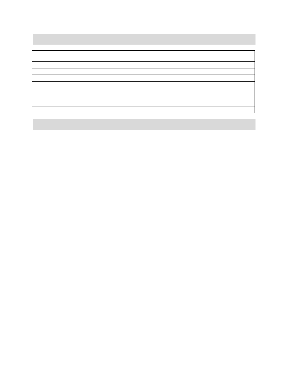
1.2 Intel
®
Server Chassis P4304XXSFCN Views
A. 365W Fixed Power supply
B. I/O Ports
C. Alternate RMM4 Knockout
D. PCI Add-in Board Slot Covers
E. AC Input Power Connector
F. Serial Port Knockout
G. A Kensington* Cable Lock Mounting Hole
H. Padlock Loop
I. Alternate RMM4 Knockout
J. Front Control Panel
K. Alternate 5.25” Peripheral Bays
L. 92x38mm System Rear Fan
M. Fixed Hard Drive Bays
Figure 1. Internal Chassis View of Intel® Server Chassis P4304XXSFCN
Revision 1.5 Intel order number G22850-006
Page 16
Product Overview Intel® Server Chassis P4000S Family TPS
4
1.3 Intel
®
Server Chassis P4304XXSHCN Views
A. 365W Fixed Power Supply
B. I/O Ports
C. Alternate RMM4 Knockout
D. PCI Add-in Board Slot Covers
E. AC Input Power Connector
F. Serial Port Knockout
G. A Kensington* Cable Lock Mounting Hole
H. Padlock Loop
I. Alternate RMM4 Knockout
J. Front Control Panel
K. 5.25” Peripheral Bays
L. 92x38mm System Rear Fan
M. 4x3.5” Hot-swap HDD Cage
Figure 2. Internal Chassis View of Intel® Server Chassis P4304XXSHCN
Intel order number G22850-006 Revision 1.5
Page 17

Intel® Server Chassis P4000S Family TPS Product Overview
5
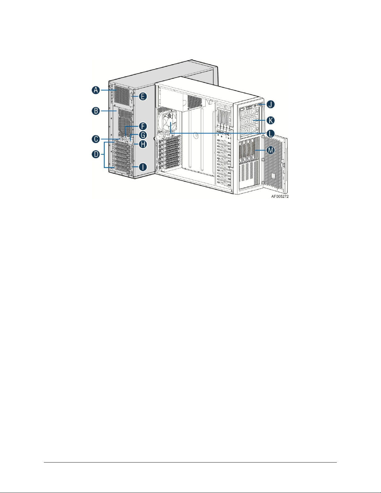
1.4 Intel
®
Server Chassis P4304XXSFEN Views
A. 550W Fixed Power supply
B. I/O Ports
C. Alternate RMM4 Knockout
D. PCI Add-in Board Slot Covers
E. AC Input Power Connector
F. Serial Port Knockout
G. A Kensington* Cable Lock Mounting Hole
H. Padlock Loop
I. Alternate RMM4 Knockout
J. Front Control Panel
K. Alternate 5.25” Peripheral Bays
L. CPU Zone System Fan
M. Fixed Hard Drive Bays
N. PCI Zone System Fan
Figure 3. Internal Chassis View of Intel® Server Chassis P4304XXSFEN
Revision 1.5 Intel order number G22850-006
Page 18

Product Overview Intel® Server Chassis P4000S Family TPS
6
1.5 Intel
®
Server Chassis P4304XXSHEN Views
A. 550W Fixed Power supply
B. I/O Ports
C. Alternate RMM4 Knockout
D. PCI Add-in Board Slot Covers
E. AC Input Power Connector
F. Serial Port Knockout
G. A Kensington* Cable Lock Mounting Hole
H. Padlock Loop
I. Alternate RMM4 Knockout
J. Front Control Panel
K. Alternate 5.25” Peripheral Bays
L. CPU Zone System Fan
M. 4x3.5” Hot-swap HDD Cage
N. PCI Zone System Fan
O. Hot-swap HDD EMI Shield
Figure 4. Internal Chassis View of Intel® Server Chassis P4304XXSHEN
Intel order number G22850-006 Revision 1.5
Page 19

Intel® Server Chassis P4000S Family TPS Product Overview
7
1.6 Intel
®
Server Chassis P4304XXSFDR Views
A. 460W Redundant Power Supply (Two)
B. AC Input Power Connector (Two)
C. I/O Ports
D. Alternate RMM4 Knockout
E. PCI Add-in Board Slot Covers
F. Serial Port Knockout
G. A Kensington* Cable Lock Mounting Hole
H. Padlock Loop
I. Alternate RMM4 Knockout
J. Front Control Panel
K. Alternate 5.25” Peripheral Bays
L. CPU Zone System Fan
M. Fixed Hard Drive Bays
N. PCI Zone System Fan
Figure 5. Internal Chassis View of Intel® Server Chassis P4304XXSFDR
Revision 1.5 Intel order number G22850-006
Page 20
Product Overview Intel® Server Chassis P4000S Family TPS
8
1.7 Intel
®
Server Chassis P4304XXSHDR Views
A. 460W Redundant Power Supply (Two)
B. AC Input Power Connector (Two)
C. I/O Ports
D. Alternate RMM4 Knockout
E. PCI Add-in Board Slot Covers
F. Serial Port Knockout
G. A Kensington* Cable Lock Mounting Hole
H. Padlock Loop
I. Alternate RMM4 Knockout
J. Front Control Panel
K. Alternate 5.25” Peripheral Bays
L. CPU Zone System Fan
M. 4x3.5” Hot-swap HDD Cage
N. PCI Zone System Fan
O. Hot-swap HDD EMI Shield
Figure 6. Internal Chassis View of Intel® Server Chassis P4304XXSHDR
1.8 Chassis Security
A variety of chassis security options are provided at the system level:
A removable padlock loop at the rear of the system access cover can be used to prevent
access to the microprocessors, memory, and add-in cards. A variety of lock sizes can be
accommodated by the 0.270-inch diameter loop.
A Kensington* cable lock mounting hole is provided on the rear chassis I/O panel.
A chassis intrusion switch is provided, allowing server management software to detect
unauthorized access to the system side cover.
Intel order number G22850-006 Revision 1.5
Page 21
Intel® Server Chassis P4000S Family TPS Product Overview
9
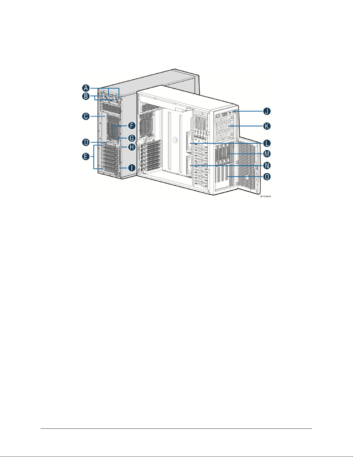
I/O Aperture
Baseboard
Datum 0,0
5.196 ± 0.0106.250 ± 0.008
1.750 ± 0.008
(0.650)
(0.150)
0.100 Min keepout around opening
R 0.039 MAX, TYP
In hot-swap hard drives configuration, a door lock is provided on the front bezel assembly
with the door to prevent access to the hot-swap hard drives and the interior of the chassis.
Note: See the technical product specification appropriate to the server board for a description of
BIOS and management security features for each specific supported platform. Technical
product specifications can be found at http://www.intel.com/p/en_US/support.
1.9 I/O Panel
All input/output (I/O) connectors are accessible from the rear of the chassis. The SSI E-bay
3.61-compliant chassis provides an ATX 2.2-compatible cutout for I/O shield installation. Boxed
Intel® server boards provide the required I/O shield for installation in the cutout. The I/O cutout
dimensions are shown in the following figure for reference.
Figure 7. ATX 2.2 I/O Aperture
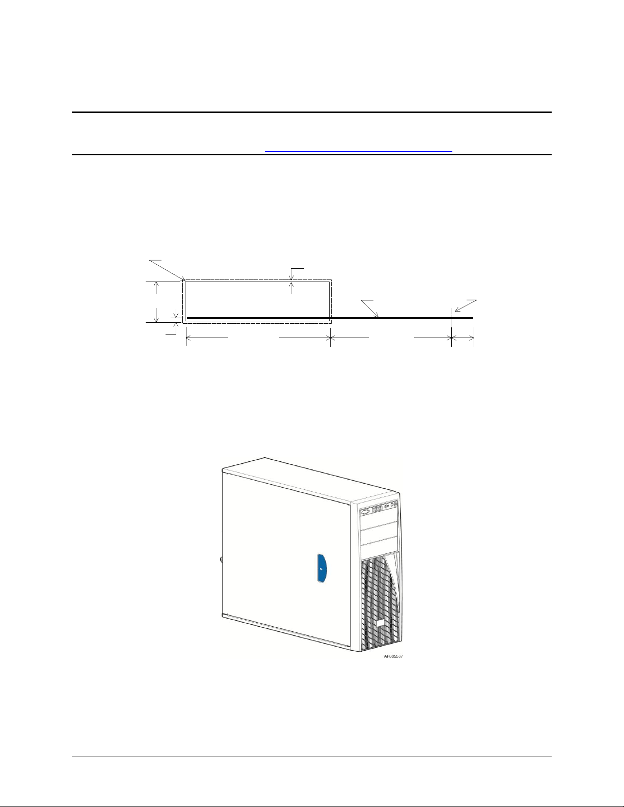
1.10 Front Bezel Features
There are two types of front bezel assembly in the Intel® Server Chassis P4000S family:
1. Front bezel assembly for fixed hard drives configuration.
Figure 8. Front Closed Chassis View with Front Bezel for Fixed Hard Drives Configuration
Revision 1.5 Intel order number G22850-006
Page 22
Product Overview Intel® Server Chassis P4000S Family TPS
10
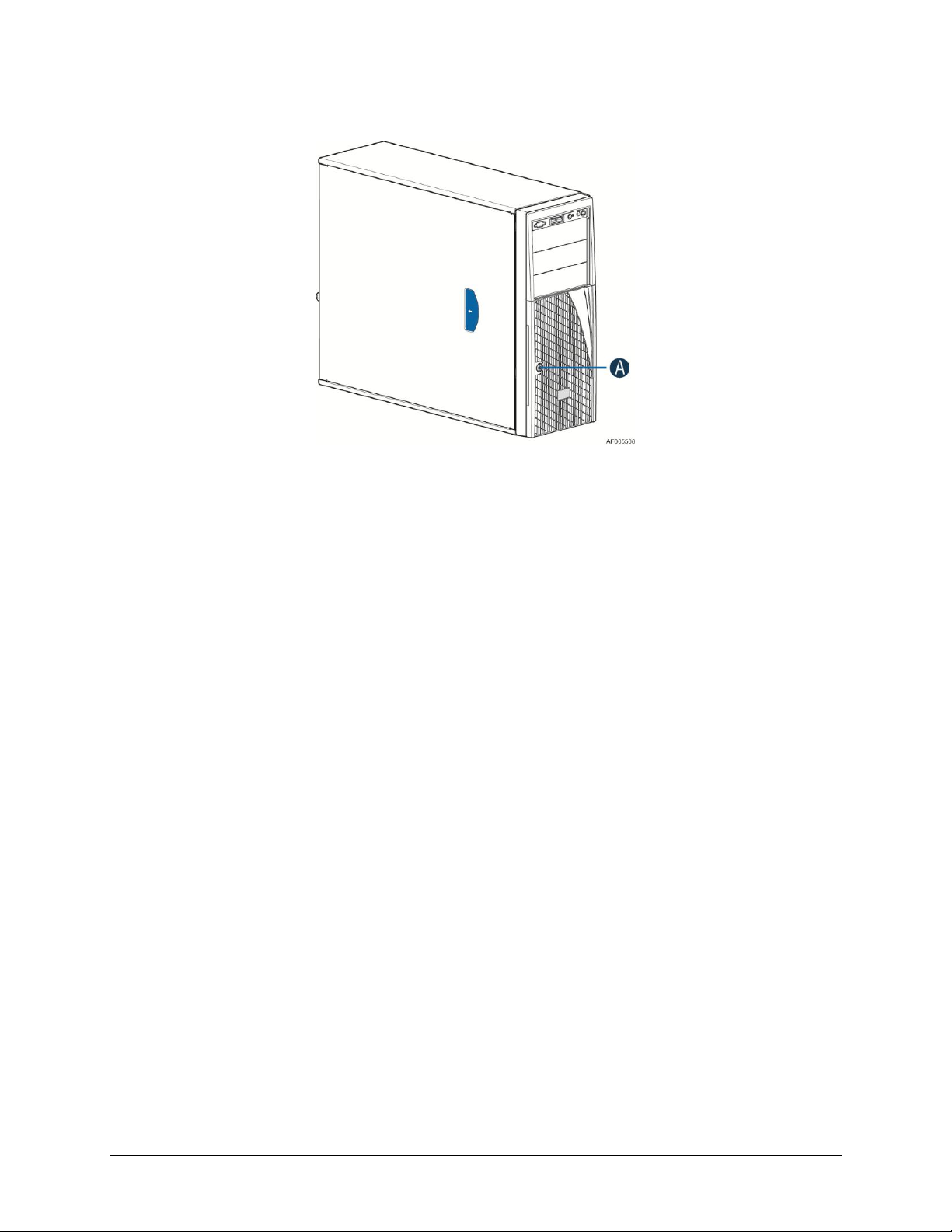
2. Front bezel assembly with the door for hot-swap hard drives configuration.
A. Security Lock
Figure 9. Front Closed Chassis View with Front Bezel for Hot-swap Hard Drives Configuration
Both two pedestal front bezel are constructed of molded plastic and attaches to the front of the
chassis with three clips on the right side and two snaps on the left. The snaps at the left attach
behind the access cover, thereby preventing accidental removal of the bezel. The bezel can
only be removed by first removing the server access cover. This provides additional security to
the hard drive and peripheral bay area.
For the front bezel assembly for fixed hard drives configuration, removing the bezel, there is an
EMI shield covering the fixed hard drives bay area.
For the front bezel assembly for hot-swap hard drives configuration, the bezel includes a keylocking door that covers the drive cage area and allows access to hot swap drives when a hot
swap drive cage is installed.
The peripheral bays are covered with plastic snap-in cosmetic pieces that must be removed to
add peripherals to the system. Front panel buttons and lights are located above the peripheral
bays.
Intel order number G22850-006 Revision 1.5
Page 23

Intel® Server Chassis P4000S Family TPS Product Overview
11
A
Fixed Power Supply
F
Serial-B Port (Optional)
B
IO Connectors
G
Kensington* Cable Lock Mounting Hole
C
RMM4 NIC Port (Optional)
H
Padlock Loop
D
Add in PCI-e cards
I
RMM4 NIC Port (Optional)
E
Power Connector
1.11 Front Panel Overview
The following figure shows the layout of the Front Control Panel of Intel® Server Chassis
P4000S:
Figure 10. Front Panel Controls and Indicators
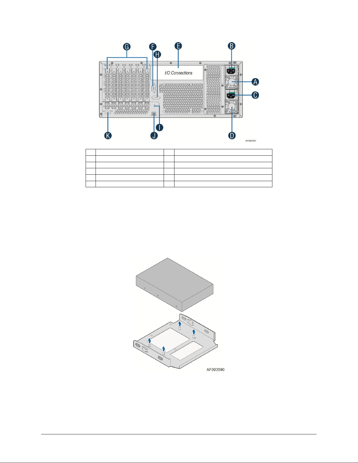
1.12 Back Panel Overview
The following figure shows the layout of Back Panel with fixed power supply and hot-swap
redundant power supplies:
Figure 11. Back Panel Layout (with Fixed Power Supply)
Revision 1.5 Intel order number G22850-006
Page 24
Product Overview Intel® Server Chassis P4000S Family TPS
12
A
Hot-swap Power Supply
G
Add in PCI-e cards
B
Power Connector
H
Serial-B Port (Optional)
C
Power Connector
I
Kensington* Cable Lock Mounting Hole
D
Hot-swap Power Supply
J
Padlock Loop
E
IO Connectors
K
RMM4 NIC Port (Optional)
F
RMM4 NIC Port (Optional)
Figure 12. Back Panel Layout (with Hot-swap Power Supply)
1.13 Standard Fixed Drive Trays
Intel® Server Chassis P4000S family supports four 3.5” fixed Hard Disk Drive trays. You can
secure each of the four drives on the drive trays with screws, and install the drive trays in the
chassis without a tool.
Intel order number G22850-006 Revision 1.5
Figure 13. Fixed Drive Tray
Page 25
Intel® Server Chassis P4000S Family TPS Product Overview
13
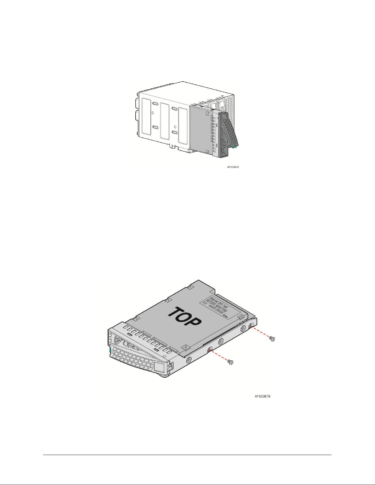
1.14 4x3.5” Hot-Swap Hard Disk Drive Cage
The Intel® Server Chassis P4000S family supports 4x3.5” hot-swap hard drive cage, which can
support up to four hot-swap hard drives.
Figure 14. 4x3.5” Hot-Swap Hard Disk Drive Cage
1.14.1 3.5” Hot-swap Hard Drive Carrier
Each hard drive must be mounted to a hot-swap drive carrier, making insertion and extraction of
the drive from the chassis very simple. Each drive carrier has its own dual-purpose latching
mechanism used to both insert and extract drives from the chassis and lock the carrier in place.
Each drive carrier supports a light pipe providing a drive status indicator, located on the
backplane, to be viewable from the front of the chassis.
The 3.5” hot-swap hard drive carrier has a 2.5” HDD interface bracket pre-installed. The 2.5”
HDD interface bracket is used to install the 2.5” hard drive on the 3.5” hot-swap hard drive
carrier. When a 3.5” hard drive is to be installed, the 2.5” HDD interface bracket should be
removed.
Figure 15. 3.5” hot-swap hard drive carrier with 2.5” HDD Interface Bracket
Revision 1.5 Intel order number G22850-006
Page 26
Product Overview Intel® Server Chassis P4000S Family TPS
14
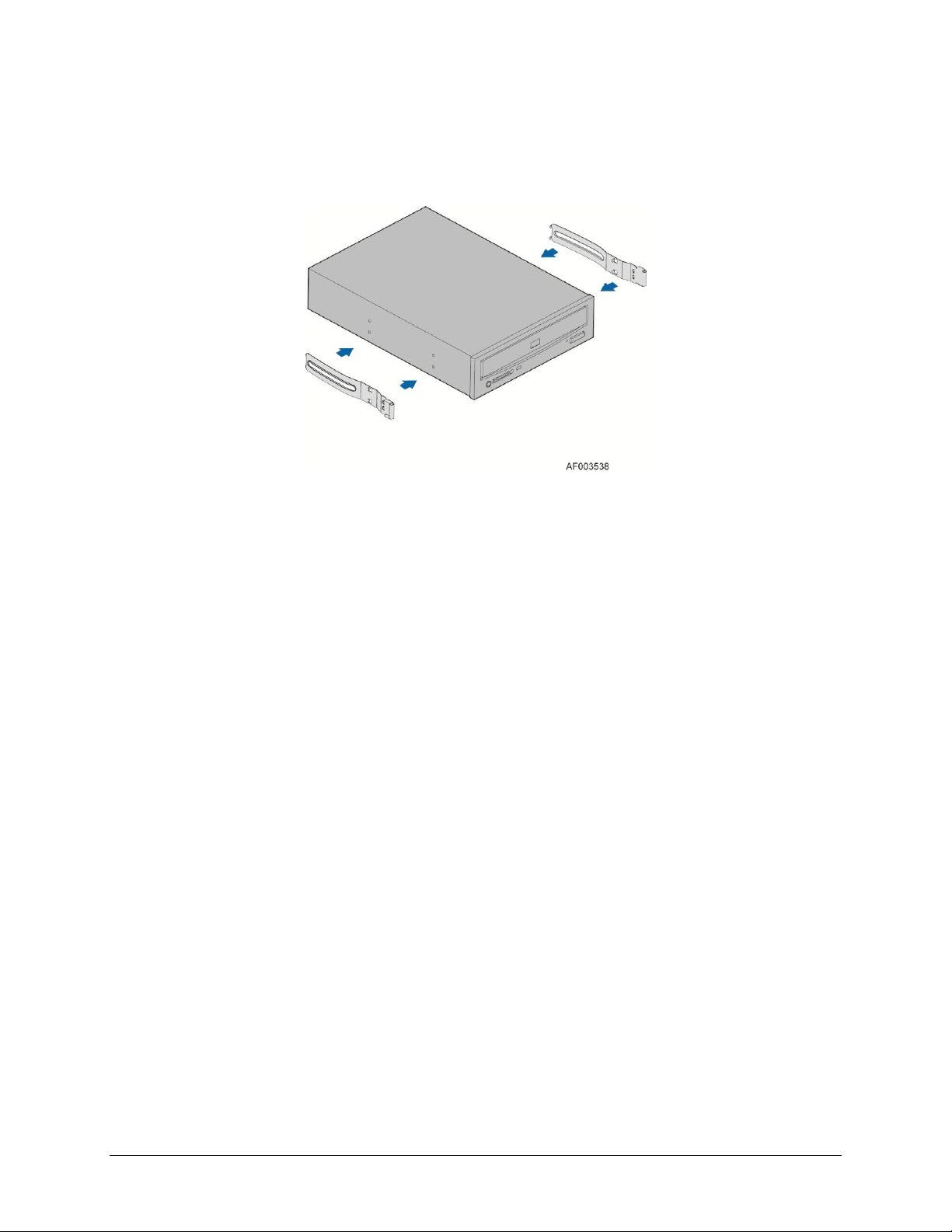
1.15 Peripheral Bays
Three 5.25-in half-height drive bays are available for CD/DVD-ROM or tape drives as well as
one 3.5-inch removable media drive bay. Drive installation is tool-less and requires no screws.
Figure 16. Tool-less Rails Mounting 5.25-inch CD-ROM Drive
Intel order number G22850-006 Revision 1.5
Page 27

Intel® Server Chassis P4000S Family TPS Chassis Power Sub-system
15
2. Chassis Power Sub-system
2.1 365W Power Supply
This 365W power supply specification defines a non-redundant power supply that supports
pedestal entry server systems. The 365W power supply has 6 outputs; 3.3V, 5V, 12V1, 12V2,
-12V, and 5Vsb. The power supply has an AC input and be power factor corrected.
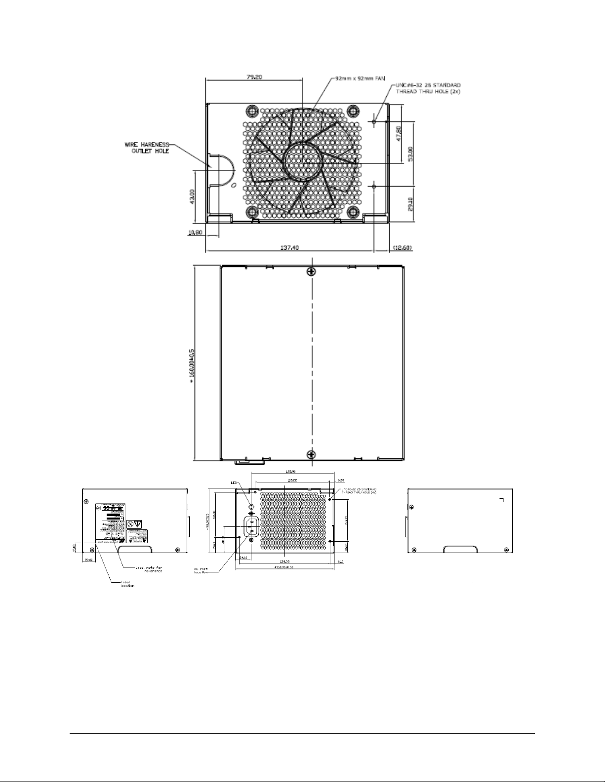
2.1.1 Mechanical Overview
The power supply size is 98mm x 150mm x 160mm (H x W x D) and has a wire harness for the
DC outputs. The AC plugs directly into the external face of the power supply.
Revision 1.5 Intel order number G22850-006
Page 28
Chassis Power Sub-system Intel® Server Chassis P4000S Family TPS
16
Figure 17. Mechanical Drawing for 365W Power Supply Enclosure
Intel order number G22850-006 Revision 1.5
Page 29
Intel® Server Chassis P4000S Family TPS Chassis Power Sub-system
17
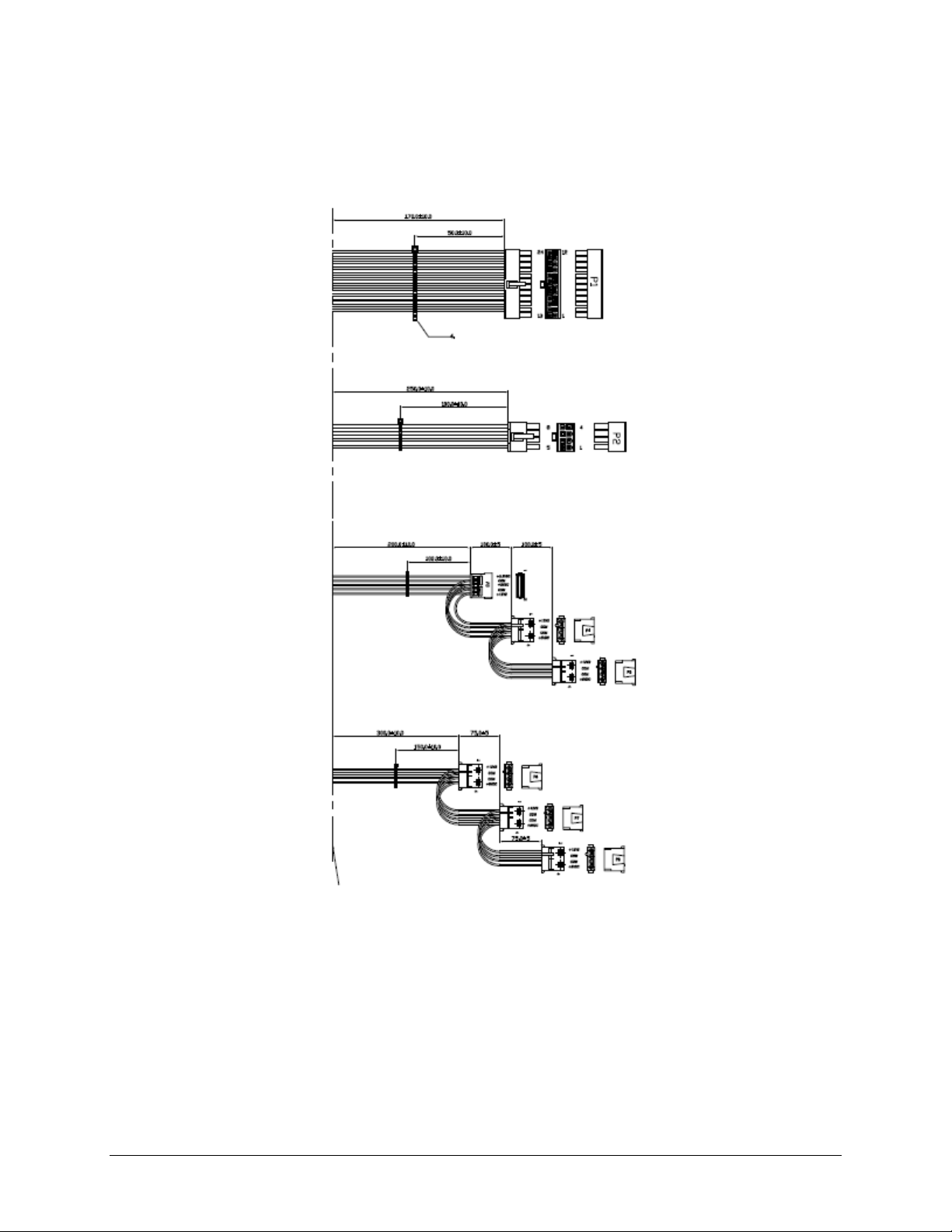
2.1.2 365W Power Supply Output Wire Harness
Listed or recognized component appliance wiring material (AVLV2), CN, rated min 85°C,
300VDC shall be used for all output wiring.
Figure 18. Output Cable Harness for 365W Power Supply
Revision 1.5 Intel order number G22850-006
Page 30
Chassis Power Sub-system Intel® Server Chassis P4000S Family TPS
18
From
Length (mm)
To connector #
No of pins
Description
Power Supply cover exit
hole
290
P1
24
Baseboard Power Connector
Power Supply cover exit
hole
250
P2 8 Processor Power Connector
Power Supply cover exit
hole
230
P3 5 SATA Power Connector
Extension from P3
100
P4 5 SATA Power Connector
Extension from P4
100
P5 4 Peripheral Power Connector
Power Supply cover exit
hole
300
P6 4 Peripheral Power Connector
Extension from P6
75
P7 4 Peripheral Power Connector
Extension from P7
75
P8 4 Peripheral Power Connector
PIN
SIGNAL
18 AWG COLOR
PIN
SIGNAL
18 AWG COLOR
1
+3.3 VDC
Orange
13
+3.3 VDC
Orange
2
+3.3 VDC
Orange
14
-12 VDC
Blue
3
COM
Black
15
COM
Black
4
+5 VDC*
Red
16
PSON#
Green
5
COM
Black
17
COM
Black
6
+5 VDC
Red
18
COM
Black
7
COM
Black
19
COM
Black
8
PWR OK
Gray
20
Reserved
N.C.
9
5VSB
Purple
21
+5 VDC
Red
10
+12V2
Yellow/Black
22
+5 VDC
Red
11
+12V2
Yellow/Black
23
+5 VDC
Red
12
+3.3 VDC
Orange
24
COM
Black
Table 2. 365W Power Supply Cable Lengths
2.1.2.1 Main power connector (P1)
Connector housing: 24- Pin Molex* Mini-Fit Jr 39-01-2245 (94V2) or equivalent
Contact: Molex* Minifit Jr, Crimp 5556 or equivalent
Table 3. P1 Main Power Connector
Intel order number G22850-006 Revision 1.5
Page 31

Intel® Server Chassis P4000S Family TPS Chassis Power Sub-system
19
PIN
SIGNAL
18 AWG COLOR
PIN
SIGNAL
18 AWG COLOR
1
COM
Black
5
+12V1
Yellow
2
COM
Black
6
+12V1
Yellow
3
COM
Black
7
+12V1
Yellow
4
COM
Black
8
+12V1
Yellow
Pin
Signal
18 AWG Color
1
+12V2
Yellow/Black
2
COM
Black
3
COM
Black
4
+5 VDC
Red
Pin
Signal
18 AWG Color
1
+3.3V
Orange
2
COM
Black
3
+5VDC
Red
4
COM
Black
5
+12V2
Yellow/Black
ITEM
DESCRIPTION
MIN
MAX
UNITS
Top
Operating temperature range.
0
50
C
T
non-op
Non-operating temperature range.
-40
70
C
Altitude
Maximum operating altitude.
3000
meters
2.1.2.2 Processor/Memory Power Connector (P2)
Connector housing: 8- Pin Molex* 39-01-2085 (94V2) or equivalent
Contact: Molex*, Mini-Fit Jr, HCS, 44476-1111 or equivalent
Table 4. P2 Processor#1 Power Connector
2.1.2.3 Peripheral Power Connectors (P4,5,6,7,8)
Connector housing: Amp 1-480424-0 or equivalent
Contact: Amp 61314-1 contact or equivalent
Table 5. Peripheral Power Connectors
2.1.2.4 SATA Hard Drive Power Connectors (P3)
Connector housing: JWT A3811H00-5P (94V2) or equivalent
Contact: JWT A3811TOP-0D or equivalent
Table 6. SATA Power Connector
2.1.3 Temperature Requirements
The power supply shall operate within all specified limits over the Top temperature range.
Table 7. Thermal Requirements
Revision 1.5 Intel order number G22850-006
Page 32

Chassis Power Sub-system Intel® Server Chassis P4000S Family TPS
20
Output power
20% load
50% load
100% load
Power factor
0.8
0.9
0.95
PARAMETER
MIN
RATED
VMAX
Start up VAC
Power Off
VAC
Voltage (110)
90 V
rms
100-127 V
rms
140 V
rms
85VAC +/4VAC
70VAC +/5VAC
Voltage (220)
180 V
rms
200-240 V
rms
264 V
rms
Frequency
47 Hz
50/60
63 Hz
Loading
Holdup time
75%
12msec
2.1.4 AC Input Requirements
2.1.4.1 Power Factor
The power supply meets the power factor requirements stated in the Energy Star® Program
Requirements for Computer Servers. These requirements are stated below:
Table 8. Power Factor Requirements for Computer Servers
Tested at 230Vac, 50Hz and 60Hz and 115VAC, 60Hz.
Tested according to Generalized Internal Power Supply Efficiency Testing Protocol Rev 6.4.3.
This is posted at http://efficientpowersupplies.epri.com/methods.asp.
2.1.4.2 AC Inlet Connector
The AC input connector is an IEC 320 C-14 power inlet. This inlet is rated for 10A/250VAC.
2.1.4.3 AC Input Voltage Specification
The power supply operates within all specified limits over the following input voltage range.
Harmonic distortion of up to 10% of the rated line voltage does not cause the power supply to
go out of specified limits. Application of an input voltage below 85VAC does not cause damage
to the power supply, including a blown fuse.
Table 9. AC Input Voltage Range
Notes:
1. Maximum input current at low input voltage range shall be measured at 90VAC, at max. load.
2. Maximum input current at high input voltage range shall be measured at 180VAC, at max. load.
3. This requirement is not to be used for determining agency input current markings.
2.1.4.4 AC Line Dropout/Holdup
An AC line dropout is defined to be when the AC input drops to 0VAC at any phase of the AC
line for any length of time. During an AC dropout the power supply meets dynamic voltage
regulation requirements. An AC line dropout of any duration does not cause tripping of control
signals or protection circuits. If the AC dropout lasts longer than the holdup time the power
supply recovers and meets all turn on requirements. The power supply meets the AC dropout
requirement over rated AC voltages and frequencies. A dropout of the AC line for any duration
does not cause damage to the power supply.
Table 10. AC Line Holdup Time
Intel order number G22850-006 Revision 1.5
Page 33

Intel® Server Chassis P4000S Family TPS Chassis Power Sub-system
21
AC Line Sag (10sec interval between each sagging)
Duration
Sag
Operating AC Voltage
Line Frequency
Performance Criteria
0 to 1/½ AC
cycle
95%
Nominal AC Voltage ranges
50/60Hz
No loss of function or performance
> 1 AC cycle
>30% Nominal AC Voltage ranges
50/60Hz
Loss of function acceptable, self
recoverable
AC Line Surge
Duration
Surge
Operating AC Voltage
Line Frequency
Performance Criteria
Continuous
10%
Nominal AC Voltages
50/60Hz
No loss of function or performance
0 to ½ AC
cycle
30%
Mid-point of nominal AC
Voltages
50/60Hz
No loss of function or performance
2.1.4.5 AC Line Fuse
The power supply has one line fused in the single line fuse on the line (Hot) wire of the AC
input. The line fusing is acceptable for all safety agency requirements. The input fuse is a slow
blow type. AC inrush current does not cause the AC line fuse to blow under any conditions. All
protection circuits in the power supply do not cause the AC fuse to blow unless a component in
the power supply has failed. This includes DC output load short conditions.
2.1.4.6 AC Line Leakage Current
The maximum leakage current to ground for each power supply is 3.5mA when tested at
240VAC.
2.1.4.7 AC Line Transient Specification
AC line transient conditions are defined as “sag” and “surge” conditions.
“Sag” conditions are
also commonly referred to as “brownout”, these conditions is defined as the AC line voltage
dropping below nominal voltage conditions. “Surge” is defined to refer to conditions when the AC
line voltage rises above nominal voltage.
The power supply meets the requirements under the following AC line sag and surge conditions.
Table 11. AC Line Sag Transient Performance
Table 12. AC Line Surge Transient Performance
2.1.4.8 Power Recovery
The power supply recovers automatically after an AC power failure. AC power failure is defined
to be any loss of AC power that exceeds the dropout criteria.
2.1.5 Efficiency
The following table provides the required minimum efficiency level at various loading conditions.
These are provided at three different load levels; 100%, 50% and 20%. Output shall be loaded
according to the proportional loading method defined by 80 Plus in Generalized Internal Power
Supply Efficiency Testing Protocol Rev 6.4.3. This is posted at
http://efficientpowersupplies.epri.com/methods.asp.
Revision 1.5 Intel order number G22850-006
Page 34

Chassis Power Sub-system Intel® Server Chassis P4000S Family TPS
22
Loading
100% of maximum
50% of maximum
20% of maximum
Minimum Efficiency
85%
88%
85%
Parameter
Min
Max.
Peak
Unit
5V
0.3
10.0
A
12V1
0.7
16.0
18.0
A
12V2
1.5
16.0
18.0
A
3.3V
0.5
18.0
A 12V
0.0
0.5 A
5Vstby
0.0
2.5
3.0
A
3.3V
5.0V
12.0V
12.0V
12.0V
5.0V
Total
Power
12V
Power
3.3V/5V
Power
Load1
10.8
2
16
10.5
0
0.3
365
318
46
Load2
18
4.1
7.6
16 0 0.3
365
283
80
Load3
18
4.1
16
7.6 0 0.3
365
283
80
Load4
13.6
7
10.2
12
0.5
2.5
365
266
80
Load5
0.5
0.3
0.7
1.5 0 0.3
31
26
3
Load6
16 4 0.7
2.6 0 0.3
114
40
73
Load7
1.2
2.7
14.5
7.1 0 1
282
259
17
Table 13. Silver Efficiency Requirement
The power supply passes with enough margins to make sure in production all power supplies
meet these efficiency requirements.
2.1.5.1 Standby Efficiency
When in standby mode; the power supply draws less than 1W AC power with 100mA of
5Vstandby load. This shall be tested at 115VAC/60Hz and 230VAC/50Hz.
2.1.6 DC Output Specification
2.1.6.1 Output Power/Currents
The following table defines the minimum power and current ratings. The power supply meets
both static and dynamic voltage regulation requirements for all conditions.
Table 14. Over Voltage Protection Limits
Notes:
1. Max. combined power for all output shall not exceed 365W.
2. Peak combined power for all outputs shall not exceed 385W.
3. Max. combined power of 12V1 and 12V2 shall not exceed 318W.
4. Max. combined power on 3.3V and 5V shall not exceed 80W.
5. Peak power and current loading shall be supported for a minimum of 12 second.
2.1.6.2 Cross Loading
The power supply maintains voltage regulation limit when operated over the following cross
loading conditions.
Table 15. Loading Conditions
Intel order number G22850-006 Revision 1.5
Page 35

Intel® Server Chassis P4000S Family TPS Chassis Power Sub-system
23
PARAMETER
TOLERANCE
MIN
NOM
MAX
UNITS
+3.3V
- 5%/+5%
+3.14
+3.30
+3.46
V
rms
+5V
- 5%/+5%
+4.75
+5.00
+5.25
V
rms
+12V1
- 5%/+5%
+11.40
+12.00
+12.60
V
rms
+12V2
- 5%/+5%
+11.40
+12.00
+12.60
V
rms
- 12V
- 10%/+10%
- 13.20
-12.00
-10.80
V
rms
+5VSB
- 5%/+5%
+4.75
+5.00
+5.25
V
rms
Output
Step Load Size
(See note 2)
Load Slew Rate
Test capacitive Load
+3.3V
6.0A
0.5 A/sec
970 F
+5V
4.0A
0.5 A/sec
400 F
12V1+12V2
18.0A
0.5 A/sec
2200 F
1,2
+5VSB
0.5A
0.5 A/sec
20 F
Output
MIN
MAX
Units
+3.3V
250
5000
F
+5V
400
5000
F
+12V
500
8000
F
2.1.6.3 Standby Output
The 5VSB output is present when an AC input greater than the power supply turn on voltage is
applied.
2.1.6.4 Voltage Regulation
The power supply output voltages stay within the following voltage limits when operating at
steady state and dynamic loading conditions. These limits include the peak-peak ripple/noise.
These shall be measured at the output connectors.
Table 16. Voltage Regulation Limits
2.1.6.5 Dynamic Loading
The output voltages remain within limits specified for the step loading and capacitive loading
specified in the table below. The load transient repetition rate is tested between 50Hz and 5kHz
at duty cycles ranging from 10%-90%. The load transient repetition rate is only a test
specification. The step load may occur anywhere within the minimum load to the maximum
load conditions.
Table 17. Transient Load Requirements
Notes:
1. Step loads on each 12V output may happen simultaneously.
2. The +12V should be tested with 2200F evenly split between the four +12V rails.
3. This will be tested over the range of load conditions in section 2.1.6.2.
2.1.6.6 Capacitive Loading
The power supply is stable and meets all requirements with the following capacitive loading
ranges.
Table 18. Capacitive Loading Conditions
Revision 1.5 Intel order number G22850-006
Page 36

Chassis Power Sub-system Intel® Server Chassis P4000S Family TPS
24
Output
MIN
MAX
Units
-12V
1
350
F
+5VSB
20
350
F
+3.3V
+5V
+12V 1
+12V 2
-12V
+5VSB
50mVp-p
50mVp-p
120mVp-p
120mVp-p
200mVp-p
50mVp-p
2.1.6.7 Grounding
The output ground of the pins of the power supply provides the output power return path. The
output connector ground pins are connected to the safety ground (power supply enclosure). This
grounding is well designed to ensure passing the maximum allowed Common Mode Noise
levels.
The power supply is provided with a reliable protective earth ground. All secondary circuits are
connected to protective earth ground. Resistance of the ground returns to chassis does not
exceed 1.0 m. This path may be used to carry DC current.
2.1.6.8 Residual Voltage Immunity in Standby mode
The power supply is immune to any residual voltage placed on its outputs (Typically a leakage
voltage through the system from standby output) up to 500mV. There is neither additional heat
generated, nor stressing of any internal components with this voltage applied to any individual
or all outputs simultaneously. It also does not trip the protection circuits during turn on.
The residual voltage at the power supply outputs for no load condition does not exceed 100mV
when AC voltage is applied and the PSON# signal is de-asserted.
2.1.6.9 Common Mode Noise
The Common Mode noise on any output does not exceed 350mV pk-pk over the frequency
band of 10Hz to 20MHz.
The measurement is made across a 100Ω resistor between each of DC outputs, including
ground at the DC power connector and chassis ground (power subsystem enclosure).
The test set-up shall use a FET probe such as Tektronix* model P6046 or equivalent.
2.1.6.10 Ripple/Noise
The maximum allowed ripple/noise output of the power supply is defined in below Table 19. This
is measured over a bandwidth of 10Hz to 20MHz at the power supply output connectors. A 10F
tantalum capacitor in parallel with a 0.1F ceramic capacitor is placed at the point of
measurement.
Table 19. Ripples and Noise
Intel order number G22850-006 Revision 1.5
Page 37

Intel® Server Chassis P4000S Family TPS Chassis Power Sub-system
25
AC HOT
POWER SUPPLY
AC NEUTRAL
V
OUT
RETURN
V
AC GROUND
LOAD
SCOPE
LOAD MUST BE
ISOLATED FROM
THE GROUND OF
THE POWER
SUPPLY
10uF
.1uF
GENERAL NOTES:
1. LOAD THE OUTPUT WITH ITS MINIMUM
LOAD CURRENT.
2. CONNECT THE PROBES AS SHOWN.
3. REPEAT THE MEASUREMENTS WITH THE
MAXIMUM LOAD ON THE OUTPUT.
SCOPE NOTE:
USE A TEKTRONIX 7834 OSCILLOSCOPE WITH 7A13 AND
DIFFERENTIAL PROBE P6055 OR EQUIVALENT.
Item
Description
MIN
MAX
UNITS
T
vout_rise
Output voltage rise time from each main output.
2
50
ms
Output rise time for the 5Vstby output.
1
25
ms
T
vout_on
All main outputs must be within regulation of
each other within this time.
50
ms
T
vout_off
All main outputs must leave regulation within this
time.
400
ms
The test set-up shall be as shown below:
Figure 19. Differential Noise test setup
Note: When performing this test, the probe clips and capacitors should be located close to the
load.
2.1.6.11 Timing Requirements
These are the timing requirements for the power supply operation. The output voltages rise from
10% to within regulation limits (T
from 1 to 25ms. The +3.3V, +5V and +12V1, +12V2 output voltages should start to rise
approximately at the same time. All outputs must rise monotonically. Each output voltage
reach regulation within 50ms (T
output voltage fall out of regulation within 400ms (T
shows the timing requirements for the power supply being turned on and off from the AC input,
with PSON held low and the PSON signal, with the AC input applied.
Revision 1.5 Intel order number G22850-006
) within 2 to 50ms, except for 5VSB - it is allowed to rise
vout_rise
) of each other during turn on the power supply. Each
vout_on
Table 20. Output Voltage Timing
) of each other during turn off. Table 21
vout_off
Page 38

Chassis Power Sub-system Intel® Server Chassis P4000S Family TPS
26
Item
Description
Min.
Max.
Units
T
sb_on_delay
Delay from AC being applied to 5VSB being
within regulation.
1500
ms
T
ac_on_delay
Delay from AC being applied to all output
voltages being within regulation.
2500
ms
T
vout_holdup
Time all output voltages stay within regulation
after loss of AC. Tested at 75% of maximum
load.
13
ms
T
pwok_holdup
Delay from loss of AC to de-assertion of PWOK.
Tested at 75% of maximum load.
12
ms
T
pson_on_delay
Delay from PSON# active to output voltages
within regulation limits.
5
400
ms
T
pson_pwok
Delay from PSON# deactivate to PWOK being
de-asserted.
50
ms
T
pwok_on
Delay from output voltages within regulation
limits to PWOK asserted at turn on.
100
500
ms
T
pwok_off
Delay from PWOK de-asserted to output
voltages (3.3V, 5V, 12V, -12V) dropping out of
regulation limits.
1
ms
T
pwok_low
Duration of PWOK being in the de-asserted state
during an off/on cycle using AC or the PSON
signal.
100
ms
T
sb_vout
Delay from 5VSB being in regulation to O/Ps
being in regulation at AC turn on.
10
1000
ms
Vout
10%
T
vout_rise
T
vout_on
T
vout_off
V1
V2
V3
Vout
Figure 20. Output Voltage Timing
Table 21. Turn On/Off Timing
Intel order number G22850-006 Revision 1.5
Page 39

Intel® Server Chassis P4000S Family TPS Chassis Power Sub-system
27
T
5VSB_holdup
Time the 5VSB output voltage stays within
regulation after loss of AC.
70
ms
Figure 21. Turn On/Off Timing (Power Supply Signals)
2.1.7 Protection Circuits
Protection circuits inside the power supply causes only the power supply’s main outputs to
shutdown. If the power supply latches-off due to a protection circuit tripping, an AC cycle OFF
for 15sec and a PSON# cycle HIGH for 1 sec must be able to reset the power supply.
2.1.7.1 Current Limit (OCP)
Overload currents applied to each tested output rail will cause the output to trip before they
reach or exceed 240 VA. If the current limits are exceeded the power supply shuts down and
latches-off. The latch will be cleared by toggling the PSON# signal or by an AC power
interruption. The power supply does not be damaged from repeated power cycling in this
condition. -12V and 5VSB is protected under over current or shorted conditions so that no
damage can occur to the power supply. 5Vsb will be auto-recovered after removing OCP limit.
2.1.7.2 Over Voltage Protection (OVP)
The power supply over voltage protection is locally sensed. The power supply shuts down and
latches-off after an over voltage condition occurs. This latch is cleared by toggling the PSON#
signal or by an AC power interruption. The table below shows the over voltage limits. The values
are measured at the output of the power supply’s pins.
maximum levels when measured at the power pins of the power supply connector during any
single point of fail. The voltage shall never trip any lower than the minimum levels when
measured at the power pins of the power supply connector. 5Vsb will be auto-recovered after
removing OVP limit.
The voltage shall never exceed the
Revision 1.5 Intel order number G22850-006
Page 40

Chassis Power Sub-system Intel® Server Chassis P4000S Family TPS
28
Output Voltage
MAX (V)
+3.3V
4.5
+5V
6.5
+12V1,2
14.5
+5VSB
6.5
Signal Type
Accepts an open collector/drain input from the system. Pull-up
to VSB located in power supply.
PSON# = Low
ON
PSON# = High or Open
OFF
MIN
MAX
Logic level low (power supply ON)
0V
1.0V
Logic level high (power supply OFF)
2.0V
5.25V
Source current, Vpson = low
4mA
Power up delay: T
pson_on_delay
5msec
400msec
PWOK delay: T
pson_pwok
50msec
Table 22. Over Voltage Protection (OVP) Limits
2.1.7.3 Over Temperature Protection (OTP)
The power supply will be protected against over temperature conditions caused by loss of fan
cooling or excessive ambient temperature. In an OTP condition the PSU will shutdown.
2.1.8 Control and Indicator Functions
The following sections define the input and output signals from the power supply.
Signals that can be defined as low true use the following convention: Signal# = low true
2.1.8.1 PSON# Input Signal
The PSON# signal is required to remotely turn on/off the power supply. PSON# is an active low
signal that turns on the +3.3V, +5V, +12V1, +12V2 and -12V power rails. When this signal is not
pulled low by the system, or left open, the outputs (except the +5VSB) turn off. This signal is
pulled to a standby voltage by a pull-up resistor internal to the power supply. Refer
Figure 21 for the timing diagram.
Table 23. PSON# Signal Characteristic
Intel order number G22850-006 Revision 1.5
Page 41

Intel® Server Chassis P4000S Family TPS Chassis Power Sub-system
29
Signal Type
Open collector/drain output from power supply. Pull-up to VSB
located in system.
PWOK = High
Power OK
PWOK = Low
Power Not OK
MIN
MAX
Logic level low voltage, Isink=4mA
0V
0.4V
Logic level high voltage, Isource=200A
2.4V
5.25V
Sink current, PWOK = low
4mA
Source current, PWOK = high
2mA
PWOK delay: Tpwok_on
100ms
500ms
PWOK rise and fall time
100sec
Power down delay: T pwok_off
1ms
1.0 V
PS is
enable
d
2.0 V
PS is
disable
d
1.0
V
2.0
Enabled
Disabled
0.3V ≤ Hysteresis ≤ 1.0V
In 1.0-2.0V input voltages range is
required
5.25V
0V
Figure 22. PSON# Required Signal Characteristic
2.1.8.2 PWOK (Power OK) Output Signal
PWOK is a power OK signal and will be pulled HIGH by the power supply to indicate that all the
outputs are within the regulation limits of the power supply. When any output voltage falls below
regulation limits or when AC power has been removed for a time sufficiently long so that power
supply operation is no longer guaranteed, PWOK will be de-asserted to a LOW state. See below
table for a representation of the timing characteristics of PWOK. The start of the PWOK delay
time shall be inhibited as long as any power supply output is in current limit.
Table 24. PWOK Signal Characteristics
2.2 550W Power Supply
This 550W power supply specification defines a non-redundant power supply that supports
pedestal entry server systems. The 550W power supply has 7 outputs; 3.3V, 5V, 12V1, 12V2,
12V3, -12V, and 5Vsb, with no less than 550W. The power supply has an AC input and is power
factor corrected.
Revision 1.5 Intel order number G22850-006
Page 42

Chassis Power Sub-system Intel® Server Chassis P4000S Family TPS
30
2.2.1 Mechanical Overview
The power supply size is 98mm x 150mm x 160mm (H x W x D) and has a wire harness for the
DC outputs. The AC plugs directly into the external face of the power supply.
Figure 23. Mechanical Drawing for 550W Power Supply Enclosure
Intel order number G22850-006 Revision 1.5
Page 43

Intel® Server Chassis P4000S Family TPS Chassis Power Sub-system
31
2.2.1.1 550W Power Supply Output Wire Harness
Listed or recognized component appliance wiring material (AVLV2), CN, rated min 85°C shall be
used for all output wiring.
Figure 24. Output Cable Harness for 550W Power Supply
Revision 1.5 Intel order number G22850-006
Page 44

Chassis Power Sub-system Intel® Server Chassis P4000S Family TPS
32
From
Length (mm)
To connector #
No of pins
Description
Power Supply cover exit hole
280
P1
24
Baseboard Power Connector
Power Supply cover exit hole
300
P2 8 Processor 0 connector
Power Supply cover exit hole
500
P3 8 Processor 1 connector
Power Supply cover exit hole
500
P4
5
SATA Peripheral Power
Connector for 5.25"
Extension from P4
100
P5
5
SATA Peripheral Power
Connector for 5.25"
Extension from P5
100
P6
4
Peripheral Power Connector
for 5.25"
Power Supply cover exit hole
600
P7
4
1x4 Legacy HSBP Power
Connector
Extension from P7
75
P8
4
1x4 Legacy HSBP Power
Connector
Power Supply cover exit hole
700
P9
4
1x4 Legacy HSBP
Power/Fixed HDD Adapter
Connection
Extension from P9
75
P10
4
1x4 Legacy HSBP
Power/Fixed HDD Adapter
Connection
Pin
Signal
18 awg color
Pin
Signal
18 awg color
1
+3.3 VDC
Orange
13
+3.3 VDC
Orange
2
+3.3 VDC
Orange
14
-12 VDC
Blue
3
COM
Black
15
COM
Black
4
+5 VDC*
Red
16
PSON#
Green
5
COM
Black
17
COM
Black
6
+5 VDC
Red
18
COM
Black
7
COM
Black
19
COM
Black
8
PWR OK
Gray
20
Reserved
N.C.
9
5VSB
Purple
21
+5 VDC
Red
10
+12V3
Yellow/Black
22
+5 VDC
Red
11
+12V3
Yellow/Black
23
+5 VDC
Red
12
+3.3 VDC
Orange
24
COM
Black
Table 25. Power Supply Cable Lengths
2.2.1.1.1 Main power connector (P1)
Connector housing: 24- Pin Molex* Mini-Fit Jr 39-01-2245 (94V2) or equivalent
Contact: Molex* Minifit Jr, Crimp 5556 or equivalent
Table 26. P1 Main Power Connector
Note: 3.3V remote sense shall be double crimped into pin 13 if needed to meet regulation limits.
Intel order number G22850-006 Revision 1.5
Page 45

Intel® Server Chassis P4000S Family TPS Chassis Power Sub-system
33
Pin
Signal
18 awg color
Pin
Signal
18 awg color
1
COM
Black
5
+12V1
Yellow
2
COM
Black
6
+12V1
Yellow
3
COM
Black
7
+12V1
Yellow
4
COM
Black
8
+12V1
Yellow
Pin
Signal
18 awg color
Pin
Signal
18 awg color
1
COM
Black
5
+12V2
Yellow
2
COM
Black
6
+12V2
Yellow
3
COM
Black
7
+12V2
Yellow
4
COM
Black
8
+12V2
Yellow
Pin
Signal
18 AWG Color
1
+12V3
Yellow/Black
2
COM
Black
3
COM
Black
4
+5 VDC
Red
Pin
Signal
18 AWG Color
1
+3.3V
Orange
2
COM
Black
3
+5VDC
Red
2.2.1.1.2 Processor/Memory Power Connector (P2)
Connector housing: 8- Pin Molex* 39-01-2085 (94V2) or equivalent
Contact: Molex*, Mini-Fit Jr, HCS, 44476-1111 or equivalent
Table 27. P2 Processor#1 Power Connector
2.2.1.1.3 Processor/Memory Power Connector (P3)
Connector housing: 8- Pin Molex* 39-01-2085 (94V2) or equivalent
Contact: Molex*, Mini-Fit Jr, HCS, 44476-1111 or equivalent
Table 28. P3 Processor#1 Power Connector
2.2.1.1.4 Peripheral Power Connectors (P6,7,8,9,10)
Connector housing: Amp 1-480424-0 or equivalent
Contact: Amp 61314-1 contact or equivalent
Table 29. Peripheral Power Connectors
2.2.1.1.5 SATA Hard Drive Power Connectors (P4, P5)
Connector housing: JWT A3811H00-5P (94V2) or equivalent
Contact: JWT A3811TOP-0D or equivalent
Table 30. SATA Power Connector
Revision 1.5 Intel order number G22850-006
Page 46

Chassis Power Sub-system Intel® Server Chassis P4000S Family TPS
34
Pin
Signal
18 AWG Color
4
COM
Black
5
+12V3
Yellow/Black
Item
Description
Min
Max
Units
Top
Operating temperature range.
0
50 º
C
T
non-op
Non-operating temperature range.
-
4
0
70 º
C
Altitude
Maximum operating altitude.
3
0
0
0
m
e
t
e
r
s
Output power
20% load
50% load
100% load
Power factor
0.8
0.9
0.95
2.2.2 Temperature Requirements
The power supply shall operate within all specified limits over the Top temperature range.
Table 31. Thermal Requirements
2.2.3 AC Input Requirements
2.2.3.1 Power Factor
The power supply meets the power factor requirements stated in the Energy Star® Program
Requirements for Computer Servers. These requirements are stated below.
Table 32. Power Factor Requirements for Computer Servers
Tested at 230Vac, 50Hz and 60Hz and 115VAC, 60Hz.
Tested according to Generalized Internal Power Supply Efficiency Testing Protocol Rev 6.4.3.
This is posted at http://efficientpowersupplies.epri.com/methods.asp.
2.2.3.2 AC Inlet Connector
The AC input connector is an IEC 320 C-14 power inlet. This inlet is rated for 10A/250VAC.
2.2.3.3 AC Input Voltage Specification
The power supply operates within all specified limits over the following input voltage range.
Harmonic distortion of up to 10% of the rated line voltage does not cause the power supply to
go out of specified limits. Application of an input voltage below 85VAC does not cause damage
to the power supply, including a blown fuse.
Intel order number G22850-006 Revision 1.5
Page 47

Intel® Server Chassis P4000S Family TPS Chassis Power Sub-system
35
Parameter
Min
Rated
Vmax
Start up vac
Power off
vac
Voltage (110)
90 V
rms
100-127 V
rms
140 V
rms
85VAC +/4VAC
70VAC +/5VAC
Voltage (220)
180 V
rms
200-240 V
rms
264 V
rms
Frequency
47 Hz
50/60
63 Hz
Loading
Holdup time
75%
12msec
Table 33. AC Input Voltage Range
Notes:
1. Maximum input current at low input voltage range shall be measured at 90VAC, at max. load.
2. Maximum input current at high input voltage range shall be measured at 180VAC, at max. load.
3. This requirement is not to be used for determining agency input current markings.
2.2.3.4 AC Line Dropout/Holdup
An AC line dropout is defined to be when the AC input drops to 0VAC at any phase of the AC
line for any length of time. During an AC dropout, the power supply meets dynamic voltage
regulation requirements. An AC line dropout of any duration does not cause tripping of control
signals or protection circuits. If the AC dropout lasts longer than the holdup time, the power
supply recovers and meets all turn on requirements. The power supply meets the AC dropout
requirement over rated AC voltages and frequencies. A dropout of the AC line for any duration
does not cause damage to the power supply.
Table 34. AC Line Holdup time
2.2.3.5 AC Line Fuse
The power supply has one line fused in the single line fuse on the line (Hot) wire of the AC
input. The line fusing is acceptable for all safety agency requirements. The input fuse is a slow
blow type. AC inrush current does not cause the AC line fuse to blow under any conditions. All
protection circuits in the power supply do not cause the AC fuse to blow unless a component in
the power supply has failed. This includes DC output load short conditions.
2.2.3.6 AC Line Leakage Current
The maximum leakage current to ground for each power supply is 3.5mA when tested at
240VAC.
2.2.3.7 AC Line Transient Specification
AC line transient conditions are defined as “sag” and “surge” conditions. “Sag” conditions are
also commonly referred to as “brownout”, these conditions is defined as the AC line voltage
dropping below nominal voltage conditions. “Surge” is defined to refer to conditions when the
AC line voltage rises above nominal voltage.
The power supply meets the requirements under the following AC line sag and surge conditions.
Revision 1.5 Intel order number G22850-006
Page 48

Chassis Power Sub-system Intel® Server Chassis P4000S Family TPS
36
AC Line Sag (10sec interval between each sagging)
Duration
Sag
Operating AC Voltage
Line Frequency
Performance Criteria
0 to ½ AC cycle
95%
Nominal AC Voltage ranges
50/60Hz
No loss of function or performance
> 1 AC cycle
>30% Nominal AC Voltage ranges
50/60Hz
Loss of function acceptable, self
recoverable
AC Line Surge
Duration
Surge
Operating AC Voltage
Line Frequency
Performance Criteria
Continuous
10%
Nominal AC Voltages
50/60Hz
No loss of function or performance
0 to ½ AC
cycle
30%
Mid-point of nominal AC
Voltages
50/60Hz
No loss of function or performance
Loading
100% of maximum
50% of maximum
20% of maximum
Minimum Efficiency
85%
88%
85%
Table 35. AC Line Sag Transient Performance
Table 36. AC Line Surge Transient Performance
2.2.3.8 Power Recovery
The power supply recovers automatically after an AC power failure. AC power failure is defined
to be any loss of AC power that exceeds the dropout criteria.
2.2.4 Efficiency
The following table provides the required minimum efficiency level at various loading conditions.
These are provided at three different load levels; 100%, 50% and 20%. Output shall be loaded
according to the proportional loading method defined by 80 Plus in Generalized Internal Power
Supply Efficiency Testing Protocol Rev 6.4.3. This is posted at
http://efficientpowersupplies.epri.com/methods.asp.
Table 37. Silver Efficiency Requirement
The power supply passes with enough margins to make sure in production all power supplies
meet these efficiency requirements.
2.2.4.1 Standby Efficiency
When in standby mode; the power supply draws less than 1W AC power with 100mA of
5Vstandby load. This is tested at 115VAC/60Hz and 230VAC/50Hz.
2.2.5 DC Output Specification
2.2.5.1 Output Power/Currents
The following tables define the minimum power and current ratings. The power supply meets
both static and dynamic voltage regulation requirements for all conditions.
Intel order number G22850-006 Revision 1.5
Page 49

Intel® Server Chassis P4000S Family TPS Chassis Power Sub-system
37
Parameter
Min
Max.
Peak
Unit
3.3V
0.5
18.0
A 5V
0.3
15.0
A 12V1
0.7
24.0
28.0
A
12V2
0.7
24.0
28.0
A
12V3
1.5
18.0
12V
0.0
0.5 A
5Vstby
0.0
3.0
3.5
A
3.3V
5.0V
12V1
12V2
12V3
-12V
5.0Vstby
Total
Power
12V
Power
3.3V/5V
Power
Load1
18
12.1
12
12
11.7
0
0.3
550
428
120
Load2
13.5
15
12
12
11.2
0.5
0.3
549
422
120
Load3
2.5 2 20
20
4.2 0 0.3
550
530
18
Load4
2.5 2 13.1
13.1
18 0 0.3
550
530
18
Load5
0.5
0.3
15
15
6.5
0.5
3
462
438
3
Load6
16 4 1 1 3.5 0 0.3
140
66
73
Load7
16
13 1 1 9 0.5
3
271
132
118
Parameter
Tolerance
Min
Nom
Max
Units
+3.3V
- 3%/+5%
+3.20
+3.30
+3.46
Vrms
+5V
- 4%/+5%
+4.80
+5.00
+5.25
Vrms
+12V1
- 4%/+5%
+11.52
+12.00
+12.60
Vrms
Table 38. Over Voltage Protection Limits
Notes:
1. Max. combined power for all output shall not exceed 550W.
2. Peak combined power for all outputs shall not exceed 630W for 20 seconds.
3. Max. combined power of 12V1, 12V2, and 12V3 shall not exceed 530W.
4. Max. combined power on 3.3V and 5V shall not exceed 120W.
2.2.5.2 Cross Loading
The power supply maintains voltage regulation limit when operated over the following cross
loading conditions.
Table 39. Loading Conditions
2.2.5.3 Standby Output
The 5VSB output is present when an AC input greater than the power supply turn on voltage is
applied.
2.2.5.4 Voltage Regulation
The power supply output voltages stay within the following voltage limits when operating at
steady state and dynamic loading conditions. These limits include the peak-peak ripple/noise.
These shall be measured at the output connectors.
Table 40. Voltage Regulation Limits
Revision 1.5 Intel order number G22850-006
Page 50

Chassis Power Sub-system Intel® Server Chassis P4000S Family TPS
38
Parameter
Tolerance
Min
Nom
Max
Units
+12V2
- 4%/+5%
+11.52
+12.00
+12.60
Vrms
+12V3
- 4%/+5%
+11.52
+12.00
+12.60
Vrms
- 12V
- 10%/+10%
- 13.20
-12.00
-10.80
Vrms
+5VSB
- 4%/+5%
+4.80
+5.00
+5.25
Vrms
Output
Step Load Size
(See note 2)
Load Slew Rate
Test capacitive Load
+3.3V
6.0A
0.5 A/sec
970 F
+5V
4.0A
0.5 A/sec
400 F
12V1+12V2 +12V3
23.0A
0.5 A/sec
2200 F
1,2
+5VSB
0.5A
0.5 A/sec
20 F
Output
Min
Max
Units
+3.3V
250
5000
F
+5V
400
5000
F
+12V
500
8000
F
-12V
1
350
F
+5VSB
20
350
F
2.2.5.5 Dynamic Loading
The output voltages remain within limits specified for the step loading and capacitive loading
specified in the table below. The load transient repetition rate is tested between 50Hz and 5kHz
at duty cycles ranging from 10%-90%. The load transient repetition rate is only a test
specification. The step load may occur anywhere within the minimum load to the maximum
load conditions.
Table 41. Transient Load Requirements
Notes:
1. Step loads on each 12V output may happen simultaneously.
2. The +12V should be tested with 2200F evenly split between the four +12V rails.
3. This will be tested over the range of load conditions in section 2.1.6.2.
2.2.5.6 Capacitive Loading
The power supply is stable and meets all requirements with the following capacitive loading
ranges.
Table 42. Capacitive Loading Conditions
2.2.5.7 Grounding
The output ground of the pins of the power supply provides the output power return path. The
output connector ground pins are connected to the safety ground (power supply enclosure).
This grounding is well designed to ensure passing the maximum allowed Common Mode Noise
levels.
The power supply is provided with a reliable protective earth ground. All secondary circuits are
connected to protective earth ground. Resistance of the ground returns to chassis does not
exceed 1.0 m. This path may be used to carry DC current.
Intel order number G22850-006 Revision 1.5
Page 51

Intel® Server Chassis P4000S Family TPS Chassis Power Sub-system
39
+3.3V
+5V
+12V 1, 2, 3
-12V
+5VSB
50mVp-p
50mVp-p
120mVp-p
200mVp-p
50mVp-p
AC HOT
POWER SUPPLY
AC NEUTRAL
V
OUT
RETURN
V
AC GROUND
LOAD
SCOPE
LOAD MUST BE
ISOLATED FROM
THE GROUND OF
THE POWER
SUPPLY
10uF
.1uF
GENERAL NOTES:
1. LOAD THE OUTPUT WITH ITS MINIMUM
LOAD CURRENT.
2. CONNECT THE PROBES AS SHOWN.
3. REPEAT THE MEASUREMENTS WITH THE
MAXIMUM LOAD ON THE OUTPUT.
SCOPE NOTE:
USE A TEKTRONIX 7834 OSCILLOSCOPE WITH 7A13 AND
DIFFERENTIAL PROBE P6055 OR EQUIVALENT.
2.2.5.8 Residual Voltage Immunity in Standby mode
The power supply is immune to any residual voltage placed on its outputs (Typically a leakage
voltage through the system from standby output) up to 500mV. There is neither additional heat
generated, nor stressing of any internal components with this voltage applied to any individual
or all outputs simultaneously. It also does not trip the protection circuits during turn on.
The residual voltage at the power supply outputs for no load condition does not exceed 100mV
when AC voltage is applied and the PSON# signal is de-asserted.
2.2.5.9 Common Mode Noise
The Common Mode noise on any output does not exceed 350mV pk-pk over the frequency
band of 10Hz to 20MHz.
The measurement is made across a 100Ω resistor between each of DC outputs, including
ground at the DC power connector and chassis ground (power subsystem enclosure).
The test set-up shall use a FET probe such as Tektronix* model P6046 or equivalent.
2.2.5.10 Ripple/Noise
The maximum allowed ripple/noise output of the power supply is defined in the table below. This
is measured over a bandwidth of 10Hz to 20MHz at the power supply output connectors. A
10F tantalum capacitor in parallel with a 0.1F ceramic capacitor is placed at the point of
measurement.
The test set-up shall be as shown below.
Note: When performing this test, the probe clips and capacitors should be located close to
the load.
2.2.5.11 Timing Requirements
These are the timing requirements for the power supply operation. The output voltages rise from
10% to within regulation limits (T
from 1 to 25ms. The +3.3V, +5V and +12V1, +12V2, +12V3 output voltages start to rise
Revision 1.5 Intel order number G22850-006
Table 43. Ripples and Noise
Figure 25. Differential Noise test setup
) within 2 to 50ms, except for 5VSB - it is allowed to rise
vout_rise
Page 52

Chassis Power Sub-system Intel® Server Chassis P4000S Family TPS
40
Item
Description
MIN
MAX
UNITS
T
vout_rise
Output voltage rise time from each main output.
2
50
ms
Output rise time for the 5Vstby output.
1
25
ms
T
vout_on
All main outputs must be within regulation of
each other within this time.
50
ms
T
vout_off
All main outputs must leave regulation within this
time.
400
ms
Item
Description
MIN
MAX
UNITS
T
sb_on_delay
Delay from AC being applied to 5VSB being
within regulation.
1500
ms
T
ac_on_delay
Delay from AC being applied to all output
voltages being within regulation.
2500
ms
Vout
10%
V1
V2
V3
T
vout_rise
T
vout_off
T
vout_on
approximately at the same time. All outputs rise monotonically. Each output voltage reach
regulation within 50ms (T
voltage fall out of regulation within 400ms (T
) of each other during turn on the power supply. Each output
vout_on
) of each other during turn off. Table 45 shows
vout_off
the timing requirements for the power supply being turned on and off by the AC input, with
PSON held low and the PSON signal, with the AC input applied. All timing requirements are met
for the cross loading condition in Table 39.
Table 44. Output Voltage Timing
Vout
Intel order number G22850-006 Revision 1.5
Figure 26. Output Voltage Timing
Table 45. Turn On/Off Timing
Page 53

Intel® Server Chassis P4000S Family TPS Chassis Power Sub-system
41
Item
Description
MIN
MAX
UNITS
T
vout_holdup
Time all output voltages stay within regulation
after loss of AC. Tested at 75% of maximum
load.
13
ms
T
pwok_holdup
Delay from loss of AC to de-assertion of PWOK.
Tested at 75% of maximum load.
12
ms
T
pson_on_delay
Delay from PSON# active to output voltages
within regulation limits.
5
400
ms
T
pson_pwok
Delay from PSON# deactivate to PWOK being
de-asserted.
50
ms
T
pwok_on
Delay from output voltages within regulation
limits to PWOK asserted at turn on.
100
500
ms
T
pwok_off
Delay from PWOK de-asserted to output
voltages (3.3V, 5V, 12V, -12V) dropping out of
regulation limits.
1
ms
T
pwok_low
Duration of PWOK being in the de-asserted state
during an off/on cycle using AC or the PSON
signal.
100
ms
T
sb_vout
Delay from 5VSB being in regulation to O/Ps
being in regulation at AC turn on.
10
1000
ms
T
5VSB_holdup
Time the 5VSB output voltage stays within
regulation after loss of AC.
70
ms
Figure 27. Turn On/Off Timing (Power Supply Signals)
2.2.6 Protection Circuits
Protection circuits inside the power supply causes only the power supply’s main outputs to shut
down. If the power supply latches-off due to a protection circuit tripping, an AC cycle OFF for
15sec and a PSON# cycle HIGH for 1sec able to reset the power supply.
Revision 1.5 Intel order number G22850-006
Page 54

Chassis Power Sub-system Intel® Server Chassis P4000S Family TPS
42
Output
Min OCP
Max OCP
+3.3V
22 A
Meet 240VA
+5V
16 A
30 A
+12V1,2
29 A
36 A
+12V3 (240VA limited)
18.5 A
20 A
-12V
No damage
5Vstby
No damage
Output Voltage
MAX (V)
+3.3V
4.5
+5V
6.5
+12V1,2,3
14.5
+5VSB
6.5
2.2.6.1 Current Limit (OCP)
Below are over current protection limits for each output. If the current limits exceed, the power
supply shuts down and latches-off. The latch will be cleared by toggling the PSON# signal or by
an AC power interruption. The power supply is not damaged from repeated power cycling in this
condition. -12V and 5VSB is protected under over current or shorted conditions so that no
damage can occur to the power supply. 5Vsb will be auto-recovered after removing OCP limit.
Table 46. Over Current Limits
2.2.6.2 Over Voltage Protection (OVP)
The power supply over voltage protection is locally sensed. The power supply shuts down and
latches-off after an over voltage condition occurs. This latch is cleared by toggling the PSON#
signal or by an AC power interruption. The table below contains the over voltage limits. The
values are measured at the output of the power supply’s pins. The voltage shall never exceed
the maximum levels when measured at the power pins of the power supply connector during
any single point of fail. The voltage shall never trip any lower than the minimum levels when
measured at the power pins of the power supply connector. 5VSB will be auto-recovered after
removing OVP limit.
Table 24. Over Voltage Protection (OVP) Limits
2.2.6.3 Over Temperature Protection (OTP)
The power supply will be protected against over temperature conditions caused by loss of fan
cooling or excessive ambient temperature. In an OTP condition the PSU will shut down.
2.2.7 Control and Indicator Functions
The following sections define the input and output signals from the power supply.
Signals that can be defined as low true use the following convention: Signal# = low true
2.2.7.1 PSON# Input Signal
The PSON# signal is required to remotely turn on/off the power supply. PSON# is an active low
signal that turns on the +3.3V, +5V, +12V1, +12V2, +12V3, and -12V power rails. When this
signal is not pulled low by the system, or left open, the outputs (except the +5VSB) turn off. This
Intel order number G22850-006 Revision 1.5
Page 55

Intel® Server Chassis P4000S Family TPS Chassis Power Sub-system
43
Signal Type
Accepts an open collector/drain input from the system. Pull-up
to VSB located in power supply.
PSON# = Low
ON
PSON# = High or Open
OFF
MIN
MAX
Logic level low (power supply ON)
0V
1.0V
Logic level high (power supply OFF)
2.0V
5.25V
Source current, Vpson = low
4mA
Power up delay: Tpson_on_delay
5msec
400msec
PWOK delay: T pson_pwok
50msec
Signal Type
Open collector/drain output from power supply. Pull-up to VSB
located in system.
PWOK = High
Power OK
PWOK = Low
Power Not OK
MIN
MAX
Logic level low voltage, Isink=4mA
0V
0.4V
Logic level high voltage, Isource=200A
2.4V
5.25V
1.0 V PS
is enabled
2.0 V PS
is disabled
1.0V
2.0V
Enabled
Disabled
0.3V ≤ Hysteresis ≤ 1.0V
In 1.0-2.0V input voltages range is required
5.25V
0V
signal is pulled to a standby voltage by a pull-up resistor internal to the power supply. Refer to
Figure 27 for the timing diagram.
Table 47. PSON# Signal Characteristic
Figure 28. PSON# Required Signal Characteristic
2.2.7.2 PWOK (Power OK) Output Signal
PWOK is a power OK signal and will be pulled HIGH by the power supply to indicate that all the
outputs are within the regulation limits of the power supply. When any output voltage falls below
regulation limits or when AC power has been removed for a time sufficiently long so that power
supply operation is no longer guaranteed, PWOK will be de-asserted to a LOW state. Refer to
Figure 27 for a representation of the timing characteristics of PWOK. The start of the PWOK
delay time shall be inhibited as long as any power supply output is in current limit.
Table 48. PWOK Signal Characteristics
Revision 1.5 Intel order number G22850-006
Page 56

Chassis Power Sub-system Intel® Server Chassis P4000S Family TPS
44
Signal Type
Open collector/drain output from power supply. Pull-up to VSB
located in system.
Sink current, PWOK = low
4mA
Source current, PWOK = high
2mA
PWOK delay: Tpwok_on
100ms
500ms
PWOK rise and fall time
100sec
Power down delay: T pwok_off
1ms
73.5mm
FCI 2x25 card
edge connector
10035388-102
A25
A1
B25
B1
3mm
Retention Latch
Airflow direction
185mm
40mm fan
8.5mm
39mm
11mm
2.3 460W Power Supply
This specification defines a 460W redundant power supply that supports server systems. The
parameters of this power supply are defined in this specification. This specification defines a
power supply with 2 outputs; 12V and 12V standby. The AC input shall be auto ranging and
power factor corrected.
2.3.1 Mechanical Overview
The physical size of the power supply enclosure is 39/40mm x 73.5mm x 185mm. The power
supply contains a single 40mm fan. The power supply has a card edge output that interfaces
with a 2x25 card edge connector in the system. The AC plugs directly into the external face of
the power supply. Refer to the following figure. All dimensions are nominal.
Figure 29. Power Supply Outline Drawing
2.3.1.1 DC Output Connector
The power supply shall use a card edge output connection for power and signal that is
compatible with a 2x25 Power Card Edge connector (equivalent to 2x25 pin configuration of the
FCI power card connector 10035388-102LF).
Intel order number G22850-006 Revision 1.5
Table 49. DC Output Selector
Page 57

Intel® Server Chassis P4000S Family TPS Chassis Power Sub-system
45
Pin
Name
Pin
Name
A1
GND
B1
GND
A2
GND
B2
GND
A3
GND
B3
GND
A4
GND
B4
GND
A5
GND
B5
GND
A6
GND
B6
GND
A7
GND
B7
GND
A8
GND
B8
GND
A9
GND
B9
GND
A10
+12V
B10
+12V
A11
+12V
B11
+12V
A12
+12V
B12
+12V
A13
+12V
B13
+12V
A14
+12V
B14
+12V
A15
+12V
B15
+12V
A16
+12V
B16
+12V
A17
+12V
B17
+12V
A18
+12V
B18
+12V
A19
PMBus* SDA
B19
A0 (SMBus* address)
A20
PMBus* SCL
B20
A1 (SMBus* address)
A21
PSON
B21
12V stby
A22
SMBAlert#
B22
Cold Redundancy Bus
A23
Return Sense
B23
12V load share bus
A24
+12V remote Sense
B24
No Connect
A25
PWOK
B25
Compatibility Check pin*
Note: Refer to the Common Hardware and Firmware Requirements for CRPS Power Supplies Specification.
2.3.1.2 Handle Retention
The power supply shall have a handle to assist extraction. The module shall be able to be
inserted and extracted without the assistance of tools. The power supply shall have a latch
which retains the power supply into the system and prevents the power supply from being
inserted or extracted from the system when the AC power cord is pulled into the power supply.
The handle shall protect the operator from any burn hazard through the use of the Intel
Corporation Industrial designed plastic handle or equivalent Intel approved material.
2.3.1.3 LED Marking and Identification
The power supply shall use a bi-color LED; Amber and Green. The following table shows the
LED states for each power supply operating state and the LED’s wavelength characteristics.
Refer to the Intel® LED Wavelength and Intensity Specification for more details.
Revision 1.5 Intel order number G22850-006
Page 58

Chassis Power Sub-system Intel® Server Chassis P4000S Family TPS
46
Min λd Wavelength
Nominal λd Wavelength
Max λd Wavelength
Units
Green
562
565
568
nm
Amber
607
610
613
nm
Power Supply Condition
LED State
Output ON and OK.
GREEN
No AC power to all power supplies.
OFF
AC present/Only 12VSB on (PS off) or PS in Cold
redundant state.
1Hz Blink GREEN
AC cord unplugged or AC power lost; with a second
power supply in parallel still with AC input power.
AMBER
Power supply warning events where the power supply
continues to operate; high temp, high power, high
current, slow fan.
1Hz Blink Amber
Power supply critical event causing a shutdown; failure,
OCP, OVP, Fan Fail.
AMBER
Power supply FW updating.
2Hz Blink GREEN
Item
Description
MIN
MAX
UNITS
T
op_sc_red
Operating temperature range;
spreadcore redundant (60%
load, 3000m, spreadcore system
flow impedance )
0
60
C
T
op_sc_nr
Operating temperature range;
spreadcore non-redundant
(100% load, 3000m, spreadcore
system flow impedance )
0
50
C
T
op_rackped_900
Operating temperature range;
rack/pedestal 900m (100% load,
900m, rack/pedestal system flow
impedance)
0
45
C
T
op_rackped_3000
Operating temperature range;
rack/pedestal 3000m (100%
load, 3000m, rack/pedestal
system flow impedance )
0
40
C
Texit
Maximum exit air temperature
681
C
T
non-op
Non-operating temperature
range.
-40
70
C
Altitude
Maximum operating altitude
3050
m
Table 50. LED Characteristics
Table 51. LED Indicator States
2.3.1.4 Temperature Requirements
The power supply shall operate within all specified limits over the Top temperature range. All
airflow shall pass through the power supply and not over the exterior surfaces of the power
supply.
Table 52. Environmental Requirements
Intel order number G22850-006 Revision 1.5
Page 59

Intel® Server Chassis P4000S Family TPS Chassis Power Sub-system
47
Output power
10% load
20% load
50% load
100% load
Power factor
> 0.65
> 0.80
> 0.90
> 0.95
Parameter
MIN
Rated
V
MAX
Startup VAC
Power Off
VAC
Voltage (110)
90 V
rms
100-127 V
rms
140 V
rms
85VAC +/4VAC
74VAC +/5VAC
Voltage (220)
180 V
rms
200-240 V
rms
264 V
rms
Frequency
47 Hz
50/60
63 Hz
Loading
Holdup time
70%
12msec
2.3.2 AC Input Requirements
2.3.2.1 Power Factor
The power supply must meet the power factor requirements stated in the Energy Star® Program
Requirements for Computer Servers. These requirements are stated below:
Tested at 230Vac, 50Hz and 60Hz and 115VAC, 60Hz
Tested according to Generalized Internal Power Supply Efficiency Testing Protocol Rev 6.4.3.
This is posted at http://efficientpowersupplies.epri.com/methods.asp.
2.3.2.2 AC Inlet Connector
The AC input connector shall be an IEC 320 C-14 power inlet. This inlet is rated for
10A/250VAC.
2.3.2.3 AC Input Voltage Specification
The power supply must operate within all specified limits over the following input voltage range.
Harmonic distortion of up to 10% of the rated line voltage must not cause the power supply to
go out of specified limits. Application of an input voltage below 85VAC shall not cause damage
to the power supply, including a blown fuse.
Table 53. AC Input Voltage Range
Notes:
1. Maximum input current at low input voltage range shall be measured at 90VAC, at max. load.
2. Maximum input current at high input voltage range shall be measured at 180VAC, at max. load.
3. This requirement is not to be used for determining agency input current markings.
2.3.2.4 AC Line Dropout/Holdup
An AC line dropout is defined to be when the AC input drops to 0VAC at any phase of the AC
line for any length of time. During an AC dropout the power supply must meet dynamic voltage
regulation requirements. An AC line dropout of any duration shall not cause tripping of control
signals or protection circuits. If the AC dropout lasts longer than the holdup time the power
supply should recover and meet all turn on requirements. The power supply shall meet the AC
dropout requirement over rated AC voltages and frequencies. A dropout of the AC line for any
duration shall not cause damage to the power supply.
Revision 1.5 Intel order number G22850-006
Page 60

Chassis Power Sub-system Intel® Server Chassis P4000S Family TPS
48
AC Line Sag (10sec interval between each sagging)
Duration
Sag
Operating AC Voltage
Line Frequency
Performance Criteria
0 to ½ AC cycle
95%
Nominal AC Voltage ranges
50/60Hz
No loss of function or performance
> 1 AC cycle
>30% Nominal AC Voltage ranges
50/60Hz
Loss of function acceptable, selfrecoverable
AC Line Surge
Duration
Surge
Operating AC Voltage
Line Frequency
Performance Criteria
Continuous
10%
Nominal AC Voltages
50/60Hz
No loss of function or performance
0 to ½ AC
cycle
30%
Mid-point of nominal AC
Voltages
50/60Hz
No loss of function or performance
2.3.2.5 AC Line 12VSBHoldup
The 12VSB output voltage should stay in regulation under its full load (static or dynamic) during
an AC dropout of 70ms min (=12VSB holdup time) whether the power supply is in ON or OFF
state (PSON asserted or de-asserted).
2.3.2.6 AC Line Fuse
The power supply shall have one line fused in the single line fuse on the line (Hot) wire of the
AC input. The line fusing shall be acceptable for all safety agency requirements. The input fuse
shall be a slow blow type. AC inrush current shall not cause the AC line fuse to blow under any
conditions. All protection circuits in the power supply shall not cause the AC fuse to blow unless
a component in the power supply has failed. This includes DC output load short conditions.
2.3.2.7 AC Line Transient Specification
AC line transient conditions shall be defined as “sag” and “surge” conditions. “Sag” conditions
are also commonly referred to as “brownout”; these conditions will be defined as the AC line
voltage dropping below nominal voltage conditions. “Surge” will be defined to refer to conditions
when the AC line voltage rises above nominal voltage.
The power supply shall meet the requirements under the following AC line sag and surge
conditions.
Table 54. AC Line Sag Transient Performance
Table 55. AC Line Surge Transient Performance
2.3.2.8 Power Recovery
The power supply shall recover automatically after an AC power failure. AC power failure is
defined to be any loss of AC power that exceeds the dropout criteria.
2.3.3 Efficiency
The following table provides the required minimum efficiency level at various loading conditions.
These are provided at three different load levels; 100%, 50%, 20%, and 10%. Output shall be
loaded according to the proportional loading method defined by 80 Plus in Generalized Internal
Power Supply Efficiency Testing Protocol Rev 6.4.3. This is posted at
http://efficientpowersupplies.epri.com/methods.asp
Intel order number G22850-006 Revision 1.5
Table 56. Gold Efficiency Requirement
Page 61

Intel® Server Chassis P4000S Family TPS Chassis Power Sub-system
49
Loading
100% of maximum
50% of maximum
20% of maximum
10% of maximum
Minimum Efficiency
88%
92%
88%
80%
Parameter
Min
Max.
Peak
2, 3
Unit
12V main
0.0
38.0
45.0
A
12Vstby 1
0.0
2.1
2.4
A
Parameter
Tolerance
MIN
NOM
MAX
UNITS
+12V
- 5%/+5%
+11.40
+12.00
+12.60
V
rms
+12V stby
- 5%/+5%
+11.40
+12.00
+12.60
V
rms
The power supply must pass with enough margins to make sure in production all power supplies
meet these efficiency requirements.
2.3.4 DC Output Specification
2.3.4.1 Output Power/Currents
The following table defines the minimum power and current ratings. The power supply must
meet both static and dynamic voltage regulation requirements for all conditions.
Table 57. Minimum Load Ratings
Notes:
1. 12Vstby must provide 4.0A with two power supplies in parallel. The Fan may start to work when stby current
>1.5A.
2. Peak combined power for all outputs shall not exceed 575W.
3. Length of time peak power can be supported is based on thermal sensor and assertion of the SMBAlert#.
signal. Minimum peak power duration shall be 20 seconds without asserting the SMBAlert# signal at
maximum operating temperature.
2.3.4.2 Standby Output
The 12VSB output shall be present when an AC input greater than the power supply turn on
voltage is applied. There should be load sharing in the standby rail. And two PSU modules
should be able to support 4A standby current.
2.3.4.3 Voltage Regulation
The power supply output voltages must stay within the following voltage limits when operating at
steady state and dynamic loading conditions. These limits include the peak-peak ripple/noise.
These shall be measured at the output connectors.
Table 58. Voltage Regulation Limits
2.3.4.4 Dynamic Loading
The output voltages shall remain within limits specified for the step loading and capacitive
loading specified in the table below. The load transient repetition rate shall be tested between
50Hz and 5kHz at duty cycles ranging from 10%-90%. The load transient repetition rate is only
a test specification. The step load may occur anywhere within the minimum load to the
maximum load conditions.
Table 59. Transient Load Requirements
Revision 1.5 Intel order number G22850-006
Page 62

Chassis Power Sub-system Intel® Server Chassis P4000S Family TPS
50
Output
Step Load Size(See
note)
Load Slew Rate
Test capacitive Load
+12VSB
1.0A
0.25 A/sec
20 F
+12V
60% of max load
0.25 A/sec
2000 F
Output
MIN
MAX
Units
+12VSB
20
3100
F
+12V
500
25000
F
Note: For dynamic condition +12V min loading is 1A.
2.3.4.5 Capacitive Loading
The power supply shall be stable and meet all requirements with the following capacitive loading
ranges.
Table 60. Capacitive Loading Conditions
2.3.4.6 Grounding
The output ground of the pins of the power supply provides the output power return path. The
output connector ground pins shall be connected to the safety ground (power supply enclosure).
This grounding should be well designed to ensure passing the maximum allowed Common
Mode Noise levels.
The power supply shall be provided with a reliable protective earth ground. All secondary
circuits shall be connected to protective earth ground. Resistance of the ground returns to
chassis shall not exceed 1.0 m. This path may be used to carry DC current.
2.3.4.7 Residual Voltage Immunity in Standby mode
The power supply should be immune to any residual voltage placed on its outputs (Typically a
leakage voltage through the system from standby output) up to 500mV. There shall be no
additional heat generated, nor stressing of any internal components with this voltage applied to
any individual or all outputs simultaneously. It also should not trip the protection circuits during
turn on.
The residual voltage at the power supply outputs for no load condition shall not exceed 100mV
when AC voltage is applied and the PSON# signal is de-asserted.
2.3.4.8 Common Mode Noise
The Common Mode noise on any output shall not exceed 350mV pk-pk over the frequency
band of 10Hz to 20MHz.
1. The measurement shall be made across a 100Ω resistor between each of DC outputs,
including ground at the DC power connector and chassis ground (power subsystem
enclosure).
2. The test set-up shall use a FET probe such as Tektronix* model P6046 or equivalent.
2.3.4.9 Hot Swap Requirements
Hot swapping a power supply is the process of inserting and extracting a power supply from an
operating power system. During this process the output voltages shall remain within the limits
with the capacitive load specified. The hot swap test must be conducted when the system is
operating under static, dynamic, and zero loading conditions. The power supply shall use a
Intel order number G22850-006 Revision 1.5
Page 63

Intel® Server Chassis P4000S Family TPS Chassis Power Sub-system
51
+12V main
+12VSB
120mVp-p
120mVp-p
AC HOT
POWER SUPPLY
AC NEUTRAL
V
OUT
RETURN
V
AC GROUND
LOAD
SCOPE
LOAD MUST BE
ISOLATED FROM
THE GROUND OF
THE POWER
SUPPLY
10uF
.1uF
GENERAL NOTES:
1. LOAD THE OUTPUT WITH ITS MINIMUM
LOAD CURRENT.
2. CONNECT THE PROBES AS SHOWN.
3. REPEAT THE MEASUREMENTS WITH THE
MAXIMUM LOAD ON THE OUTPUT.
SCOPE NOTE:
USE A TEKTRONIX 7834 OSCILLOSCOPE WITH 7A13 AND
DIFFERENTIAL PROBE P6055 OR EQUIVALENT.
latching mechanism to prevent insertion and extraction of the power supply when the AC power
cord is inserted into the power supply.
2.3.4.10 Forced Load Sharing
The +12V output will have active load sharing. The output will share within 10% at full load. The
failure of a power supply should not affect the load sharing or output voltages of the other
supplies still operating. The supplies must be able to load share in parallel and operate in a hotswap/redundant 1+1 configurations. The 12VSBoutput is not required to actively share current
between power supplies (passive sharing). The 12VSB output of the power supplies are
connected together in the system so that a failure or hot swap of a redundant power supply
does not cause these outputs to go out of regulation in the system.
2.3.4.11 Ripple/Noise
The maximum allowed ripple/noise output of the power supply is defined in the table below. This
is measured over a bandwidth of 10Hz to 20MHz at the power supply output connectors. A
10F tantalum capacitor in parallel with a 0.1F ceramic capacitor is placed at the point of
measurement.
Table 61. Ripples and Noise
The test set-up shall be as shown below.
Figure 30. Differential Noise test setup
Note: When performing this test, the probe clips and capacitors should be located close to the
load.
2.3.4.12 Timing Requirements
These are the timing requirements for the power supply operation. The output voltages must
rise from 10% to within regulation limits (T
) within 5 to 70ms. For 12VSB, it is allowed to
vout_rise
rise from 1.0 to 25ms. All outputs must rise monotonically. Table below shows the timing
requirements for the power supply being turned on and off by the AC input, with PSON held low
and the PSON signal, with the AC input applied.
Revision 1.5 Intel order number G22850-006
Page 64

Chassis Power Sub-system Intel® Server Chassis P4000S Family TPS
52
Item
Description
MIN
MAX
UNITS
T
vout_rise
Output voltage rise time
5.0 *
70 *
ms
Tsb_on_delay
Delay from AC being applied to 12VSBbeing
within regulation.
1500
ms
Tac_on_delay
Delay from AC being applied to all output
voltages being within regulation.
3000
ms
Tvout_holdup
Time 12V output voltage stays within
regulation after loss of AC at 70% load.
13 ms
Tpwok_holdup
Delay from loss of AC to de-assertion of
PWOK
12 ms
Tpson_on_delay
Delay from PSON# active to output voltages
within regulation limits.
5
400
ms
Tpson_pwok
Delay from PSON# deactivate to PWOK
being de-asserted.
5 ms
Tpwok_on
Delay from output voltages within regulation
limits to PWOK asserted at turn on.
100
500
ms
T pwok_off
Delay from PWOK de-asserted to output
voltages dropping out of regulation limits.
1 ms
Tpwok_low
Duration of PWOK being in the de-asserted
state during an off/on cycle using AC or the
PSON signal.
100 ms
Tsb_vout
Delay from 12VSBbeing in regulation to O/Ps
being in regulation at AC turn on.
50
1000
ms
T12VSB_holdup
Time the 12VSBoutput voltage stays within
regulation after loss of AC.
70 ms
Table 62. Timing Requirements
* The 12VSBoutput voltage rise time shall be from 1.0ms to 25ms
Intel order number G22850-006 Revision 1.5
Page 65

Intel® Server Chassis P4000S Family TPS Chassis Power Sub-system
53
Output VOLTAGE
Input voltage range
Over Current Limits
+12V
90 – 264VAC
47A min; 55A max
12VSB
90 – 264VAC
2A min; 2.5A max
Figure 31. Turn On/Off Timing (Power Supply Signals)
2.3.5 Protection Circuits
Protection circuits inside the power supply shall cause only the power supply’s main outputs to
shut down. If the power supply latches-off due to a protection circuit tripping, an AC cycle OFF
for 15sec and a PSON# cycle HIGH for 1sec shall be able to reset the power supply.
2.3.5.1 Current Limit (OCP)
The power supply shall have current limit to prevent the outputs from exceeding the values
shown in table below. If the current limits are exceeded the power supply shall shutdown and
latch off. The latch will be cleared by toggling the PSON# signal or by an AC power interruption.
The power supply shall not be damaged from repeated power cycling in this condition. 12VSB
will be auto-recovered after removing OCP limit.
Table 63. Over Current Protection
Revision 1.5 Intel order number G22850-006
Page 66

Chassis Power Sub-system Intel® Server Chassis P4000S Family TPS
54
Output Voltage
MIN (V)
MAX (V)
+12V
13.3
14.5
+12VSB
13.3
14.5
Signal Type
Accepts an open collector/drain input from the system.
Pull-up to VSB located in power supply.
PSON# = Low
ON
PSON# = High or Open
OFF
MIN
MAX
Logic level low (power supply ON)
0V
1.0V
Logic level high (power supply OFF)
2.0V
3.46V
Source current, Vpson = low
4mA
Power up delay: T
pson_on_delay
5msec
400msec
PWOK delay: T
pson_pwok
50msec
2.3.5.2 Over Voltage Protection (OVP)
The power supply over voltage protection shall be locally sensed. The power supply shall
shutdown and latces-off after an over voltage condition occurs. This latch shall be cleared by
toggling the PSON# signal or by an AC power interruption. The values are measured at the
output of the power supply’s connectors. The voltage shall never exceed the maximum levels
when measured at the power connectors of the power supply connector during any single point
of fail. The voltage shall never trip any lower than the minimum levels when measured at the
power connector. 12VSBwill be auto-recovered after removing OVP limit.
Table 64. Over Voltage Protection (OVP) Limits
2.3.5.3 Over Temperature Protection (OTP)
The power supply will be protected against over temperature conditions caused by loss of fan
cooling or excessive ambient temperature. In an OTP condition the PSU will shut down. When
the power supply temperature drops to within specified limits, the power supply shall restore
power automatically, while the 12VSB remains always on. The OTP circuit must have built in
margin such that the power supply will not oscillate on and off due to temperature recovering
condition. The OTP trip level shall have a minimum of 4C of ambient temperature margin.
2.3.6 Control and Indicator Functions
The following sections define the input and output signals from the power supply.
Signals that can be defined as low true use the following convention: Signal# = low true
2.3.6.1 PSON# Input Signal
The PSON# signal is required to remotely turn on/off the power supply. PSON# is an active low
signal that turns on the +12V power rail. When this signal is not pulled low by the system, or left
open, the outputs (except the +5VSB) turn off. This signal is pulled to a standby voltage by a
pull-up resistor internal to the power supply. Refer Figure 31 for the timing diagram.
Table 65. PSON# Signal Characteristic
Intel order number G22850-006 Revision 1.5
Page 67
Intel® Server Chassis P4000S Family TPS Chassis Power Sub-system
55
Signal Type
Open collector/drain output from power supply. Pull-up
to VSB located in the power supply.
PWOK = High
Power OK
PWOK = Low
Power Not OK
MIN
MAX
Logic level low voltage, Isink=400uA
0V
0.4V
Logic level high voltage, Isource=200A
2.4V
3.46V
Sink current, PWOK = low
400uA
Source current, PWOK = high
2mA
PWOK delay: T
pwok_on
100ms
1000ms
PWOK rise and fall time
100sec
Power down delay: T
pwok_off
1ms
200msec
1.0 V
PS is
enabled
2.0 V
PS is
disabled
1.0V
2.0V
Enabled
Disabled
0.3V ≤ Hysteresis ≤ 1.0V
In 1.0-2.0V input voltages range is required
3.46V
0V
Figure 32. PSON# Required Signal Characteristic
2.3.6.2 PWOK (Power OK) Output Signal
PWOK is a power OK signal and will be pulled HIGH by the power supply to indicate that all the
outputs are within the regulation limits of the power supply. When any output voltage falls below
regulation limits or when AC power has been removed for a time sufficiently long so that power
supply operation is no longer guaranteed, PWOK will be de-asserted to a LOW state. See the
table below for a representation of the timing characteristics of PWOK. The start of the PWOK
delay time shall be inhibited as long as any power supply output is in current limit.
Table 66. PWOK Signal Characteristics
A recommended implementation of the Power Ok circuits is shown below.
Note: The Power Ok circuits should be compatible with 5V pull up resistor (>10k) and 3.3V pull
up resistor (>6.8k).
Revision 1.5 Intel order number G22850-006
Page 68

Chassis Power Sub-system Intel® Server Chassis P4000S Family TPS
56
Q2
2N4401
PWOK out
PWOK in
Q1
2N4401
12V
3.3VSB
R2
20
R4
820
R3
10k
R1
10k
Signal Type (Active Low)
Open collector/drain output from power supply. Pull-
up to VSB located in system.
Alert# = High
OK
Alert# = Low
Power Alert to system
MIN
MAX
Logic level low voltage, Isink=4 mA
0 V
0.4 V
Logic level high voltage, Isink=50 A
3.46 V
Sink current, Alert# = low
4 mA
Sink current, Alert# = high
50 A
Alert# rise and fall time
100 s
Figure 33. Implementation of the Power Ok Circuits
2.3.6.3 SMBAlert# Signal
This signal indicates that the power supply is experiencing a problem that the user should
investigate. This shall be asserted due to Critical events or Warning events. The signal shall
activate in the case of critical component temperature reached a warning threshold, general
failure, over-current, over-voltage, under-voltage, failed fan. This signal may also indicate the
power supply is reaching its end of life or is operating in an environment exceeding the specified
limits. This signal is to be asserted in parallel with LED turning solid Amber or blink Amber.
Table 67. SMBAlert# Signal Characteristics
2.3.7 Thermal CLST
The power supply shall assert the SMBAlert signal when a temperature sensor crosses a
warning threshold. Refer to the Intel® Common Hardware and Firmware Requirements for
CRPS Power Supplier for detailed requirements.
2.3.8 Power Supply Diagnostic “Black Box”
The power supply shall save the latest PMBus* data and other pertinent data into nonvolatile
memory when a critical event shuts down the power supply. This data shall be accessible from
the SMBus* interface with an external source providing power to the 12Vstby output.
Intel order number G22850-006 Revision 1.5
Page 69

Intel® Server Chassis P4000S Family TPS Chassis Power Sub-system
57
Refer to Intel® Common Hardware and Firmware Requirements for CRPS Power Supplier for
detailed requirements.
2.3.9 Firmware Uploader
The power supply shall have the capability to update its firmware from the PMBus* interface
while it is in standby mode. This FW can be updated when in the system and in standby mode
and outside the system with power applied to the 12Vstby pins.
Refer to the Intel® Common Hardware and Firmware Requirements for CRPS Power Supplier
for detailed requirements.
2.4 Lower Current Common Redundant Power Distribution Board (PDB)
The Power Distribution Board (PDB) for Intel® Server Chassis P4000M supports the Common
Redundant power supply in a 1+1 redundant configuration. The PDB is designed to plug directly
to the output connector of the PS and it contains four DC/DC power converters to produce other
required voltages: -12V, +3.3VDC, +5VDC, and 5V standby along with additional over current
protection circuit for the 12V rails.
This power distribution board is intended to be used in the Intel® Server Chassis P4000M
Family with various common redundant power supplies: 460W, 750W and DC input 750W.
Revision 1.5 Intel order number G22850-006
Page 70

Chassis Power Sub-system Intel® Server Chassis P4000S Family TPS
58
2.4.1 Mechanical Overview
Figure 34. Outline Drawing
Intel order number G22850-006 Revision 1.5
Page 71

Intel® Server Chassis P4000S Family TPS Chassis Power Sub-system
59
Item
Description
Min
Max
Units
Top
Operating temperature range.
0
50
C
T
non-op
Non-operating temperature range.
-40
70
C
Airflow direction
Rear power supply
Front power supply
PDB
2.4.1.1 Airflow Requirements
The power distribution board shall get enough airflow for cooling DC/DC converters from the
fans located in the Power Supply modules. Following is a basic drawing showing airflow
direction.
The amount of cooling airflow that will be available to the DC/DC converters is to be no less
than 1.2M/s.
Figure 35. Airflow Diagram
2.4.1.2 DC/DC converter cooling
The DC/DC converters on the power distribution board are in series airflow path with the power
supplies.
2.4.1.3 Temperature Requirements
The PDB operates within all specified limits over the Top temperature range. Some amount of
airflow shall pass over the PDB.
Tabel 68. Thermal Requirements
2.4.1.4 Efficiency
Each DC/DC converter shall have a minimum efficiency of 85% at 50% ~ 100% loads and over
+12V line voltage range and over temperature and humidity range.
2.4.2 DC Output Specification
2.4.2.1 Input Connector (power distribution mating connector)
The power distribution provides 2 power pin, a card edge output connection for power and
signal that is compatible with a 2x25 Power Card Edge connector (equivalent to 2x25 pin
configuration of the FCI power card connector 10035388-102LF). The FCI power card edge
connector is a new version of the PCE from FCI used to raise the card edge by 0.031” to allow
for future 0.093” PCBs in the system. The card edge connector has no keying features; the
keying method is accomplished by the system sheet metal.
Revision 1.5 Intel order number G22850-006
Page 72

Chassis Power Sub-system Intel® Server Chassis P4000S Family TPS
60
Pin
Name
Pin
Name
A1
GND
B1
GND
A2
GND
B2
GND
A3
GND
B3
GND
A4
GND
B4
GND
A5
GND
B5
GND
A6
GND
B6
GND
A7
GND
B7
GND
A8
GND
B8
GND
A9
GND
B9
GND
A10
+12V
B10
+12V
A11
+12V
B11
+12V
A12
+12V
B12
+12V
A13
+12V
B13
+12V
A14
+12V
B14
+12V
A15
+12V
B15
+12V
A16
+12V
B16
+12V
A17
+12V
B17
+12V
A18
+12V
B18
+12V
A19
PMBus* SDA
B19
A0 (SMBus* address)
A20
PMBus* SCL
B20
A1 (SMBus* address)
A21
PSON
B21
12V stby
A22
SMBAlert#
B22
Cold Redundancy Bus
A23
Return Sense
B23
12V load share
A24
+12V remote Sense
B24
No Connect
A25
PWOK
B25
Compatibility Pin
From
Length,
mm
To connector #
No. of
pins
Description
Power Supply cover exit hole
470
P1
24
Baseboard Power Connector
Power Supply cover exit hole
320
P2 8 Processor 0 connector
Power Supply cover exit hole
450
P3 8 Processor 1 connector
Power Supply cover exit hole
800
P4 5 Power FRU/PMBus* connector
Power Supply cover exit hole
350
P5 5 SATA peripheral power connector for 5.25"
Extension from P5
100
P6 5 SATA peripheral power connector for 5.25"
Extension from P6
100
P7
4
Peripheral Power Connector for 5.25"/HSBP
Power
Power Supply cover exit hole
400
P8 4 1x4 legacy HSBP Power Connector
Extension from P8
75
P9 4 1x4 legacy HSBP Power Connector
Power supply cover exit hole
500
P10
4
1x4 legacy HSBP Power/Fixed HDD
adaptor Connection
Table 69. Input Connector and Pin Assignment Diagrams
2.4.2.2 Output Wire Harness
The power distribution board has a wire harness output with the following connectors.
Listed or recognized component appliance wiring material (AVLV2), CN, rated min 85°C shall be
used for all output wiring.
Table 70. PDB Cable Length
Intel order number G22850-006 Revision 1.5
Page 73

Intel® Server Chassis P4000S Family TPS Chassis Power Sub-system
61
From
Length,
mm
To connector #
No. of
pins
Description
Extension from P10
75
P11
4
1x4 legacy HSBP Power/Fixed HDD
adaptor Connection
Connector only (no cable)
P12
4
2x2 Legacy PCI Power Connector for PCIe
slots
Pin
Signal
18 AWG Color
Pin
Signal
18 AWG Color
1
+3.3VDC
Orange
13
+3.3VDC
Orange
3.3V RS
Orange (24AWG)
2 +3.3VDC
Orange
14
-12VDC
Blue
3
COM
Black
15
COM
Black
4
+5VDC
Red
16
PSON#
Green (24AWG)
5
COM
Black
17
COM
Black
6
+5VDC
Red
18
COM
Black
7
COM
Black
19
COM
Black
8
PWR OK
Gray (24AWG)
20
Reserved
N.C.
9
5 VSB
Purple
21
+5VDC
Red
10
+12V1
Yellow
22
+5VDC
Red
11
+12V1
Yellow
23
+5VDC
Red
12
+3.3VDC
Orange
24
COM
Black
Pin
Signal
18 AWG color
Pin
Signal
18 AWG Color
1
COM
Black
5*
+12V1
Yellow
2
COM
Black
6
+12V1
Yellow
3
COM
Black
7
+12V1
Yellow
4
COM
Black
8
+12V1
Yellow
Pin
Signal
18 AWG color
Pin
Signal
18 AWG Color
2.4.2.2.1 Baseboard power connector (P1)
Connector housing: 24-Pin Molex* Mini-Fit Jr. 39-01-2245 or equivalent
Contact: Molex* Mini-Fit, HCS Plus, Female, Crimp 44476 or equivalent
Table 71. P1 Baseboard Power Connector
2.4.2.2.2 Processor#0 Power Connector (P2)
Connector housing: 8-Pin Molex* 39-01-2080 or equivalent
Contact: Molex* Mini-Fit, HCS Plus, Female, Crimp 44476 or equivalent
Table 72. P0 Processor Power Connector
2.4.2.2.3 Processor#1 Power Connector (P3)
Connector housing: 8-Pin Molex* 39-01-2080 or equivalent
Contact: Molex* Mini-Fit, HCS Plus, Female, Crimp 44476 or equivalent
Table 73. P1 Processor Power Connector
Revision 1.5 Intel order number G22850-006
Page 74

Chassis Power Sub-system Intel® Server Chassis P4000S Family TPS
62
Pin
Signal
18 AWG color
Pin
Signal
18 AWG Color
1
COM
Black
5
+12V1
Yellow
2
COM
Black
6
+12V1
Yellow
3
COM
Black
7
+12V1
Yellow
4
COM
Black
8
+12V1
Yellow
Pin
Signal
24 AWG Color
1
I2C Clock
White
2
I2C Data
Yellow
3
SMBAlert#
Red 4 COM
Black
5
3.3RS
Orange
Pin
Signal
18 AWG color
Pin
Signal
18 AWG Color
1
COM
Black
3
+12V1
Yellow
2
COM
Black
4
+12V1
Yellow
Pin
Signal
18 AWG Color
1
+12V3
White
2
COM
Black
3
COM
Black
4
+5 VDC
Red
Pin
Signal
18 AWG Color
1
+12V2
Brown
2
COM
Black
3
COM
Black
4
+5 VDC
Red
2.4.2.2.4 Power Signal Connector (P4)
Connector housing: 5-pin Molex* 50-57-9405 or equivalent
Contacts: Molex* 16-02-0087 or equivalent
Table 74. Power Signal Connector
2.4.2.2.5 Aux baseboard power connector (P12)
Connector header: Foxconn* p/n HM3502E-P1 or equivalent
Table 75. Aux baseboard power connector
2.4.2.2.6 Legacy 1x4 Peripheral Power Connectors (P7, P8, P9, P10, P11)
Connector housing: Molex* 0015-24-4048 or equivalent;
Contact: Molex* 0002-08-1201 or equivalent
Table 76. P8, P9, P10, P11 Legacy Peripheral Power Connectors
Table 77. P7 Legacy Peripheral Power Connectors
Intel order number G22850-006 Revision 1.5
Page 75

Intel® Server Chassis P4000S Family TPS Chassis Power Sub-system
63
Pin
Signal
18 AWG Color
1
+3.3VDC
Orange
2
COM
Black
3
+5VDC
Red
4
COM
Black
5
+12V2
Brown
Converter
+ sense location
- sense location
Power supply main 12V
On PDB
On PDB
12V/3.3V
P20 (1x5 signal connector)
P20 (1x5 signal connector)
12V/5V
On PDB
On PDB
12V/-12V
none
none
12Vstby/5Vstby
none
none
Characteristic
Requirement
+3.3V remote sense input
impedance
200 (measure from +3.3V on P1 2x12 connector to +3.3V sense
on P20 1x5 signal connector)
+3.3V remote sense drop
200mV (remote sense must be able to regulate out 200mV drop
on the +3.3V and return path; from the 2x12 connector to the
remote sense points)
Max remote sense current draw
< 5mA
2.4.2.2.7 SATA 1x5 Peripheral Power Connectors (P5, P6)
Connector housing: Molex* 0675-82-0000 or equivalent;
Contact: Molex* 0675-81-0000 or equivalent
Table 78. SATA Peripheral Power Connectors
2.4.2.3 Grounding
The ground of the pins of the PDB output connectors provides the power return path. The output
connector ground pins is connected to safety ground (PDB enclosure). This grounding is well
designed to ensure passing the maximum allowed Common Mode Noise levels.
2.4.2.4 Remote Sense
The following table lists the remote sense requirements and connection points for all the
converters on the PDB and the main 12V output of the power supply.
Table 79. Remote Sense Connection Points
Table 80. Remote Sense Requirements
Revision 1.5 Intel order number G22850-006
Page 76

Chassis Power Sub-system Intel® Server Chassis P4000S Family TPS
64
P2
P3
P12
P1
P8
P9
P10
P11
P5,6,7
2x4
2x2
2x12
1x4
1x4
1x4
1x4
(2) 1x5,
1x4 OCP CPU1
Memory1
CPU2
Memory2
PCIe
Fans
Misc
HDD and peripherals
Total
Current
Min
Nomina
l
Max
12V1
17.8
A
10.5 A
17.8
10.5
21.7
10.0 A
3.0
A
91 A
50
55
60
12V2
18.0 A (P8, 9, 10, 11)
18 A
18
19
20
12V3
18a (P5, 6, 7)
18 A
18
19
20
P8
P9
P10
P11
P5
P6
P7
1x4
1x4
1x4
1x4
1x5
1x5
1x4
18
3 x 2.5" 8xHDD BP
HDD1
8 x 2.5
HDD2
8 x 2.5
na
na
na
na
HDD3
8 x 2.5
2 x 3.5" 4xHDD
BP
HDD1
4x3.5
HDD1
4x3.5
peripheral bay
1 x 3.5" 8xHDD
BP
HDD1
8x3.5
na
na
peripheral bay
8 x 3.5" fixed
SATA
2xfixed
2xfixed
2xfixed
2xfixed
peripheral bay
8 x 3.5" fixed
SAS
2xfixed
2xfixed
2xfixed
2xfixed
peripheral bay
2.4.2.5 12V Rail Distribution
The following table shows the configuration of the 12V rails and what connectors and
components in the system they are powering.
Table 81. 12V Rail Distribution
Note:
+12V current to PCIe slots may be supplied from four different connectors. 12V1 on P2, 12V2 on P3, 12V3 on
P1, and 12V3 on P12. P12 is reserved for board that needs 4 x GPU cards powered. P1 is the main 12V power
for PCIe slot; but additional 12V power can be connected to P2 and/or P3. The motherboard MUST NOT short
any of the 12V rails or connectors together.
2.4.2.6 Hard Drive 12V rail configuration options
The following table shows the hard drive configuration options using the defined power
connectors. In some cases additional converter or ‘Y’ cables are needed.
Table 82. Hard Drive 12V rail configuration options
Intel order number G22850-006 Revision 1.5
Page 77

Intel® Server Chassis P4000S Family TPS Chassis Power Sub-system
65
+12VDC Input DC/DC
Converters
+3.3V Converter
+5V Converter
-12V Converter
MAX Load
15A
15A
0.5A
MIN Static/Dynamic Load
0A
0A
0A
Max Output Power
3.3V x15A =49.5W
5V x15A =75W
12V x0.5A =6W
12V stby/5V stby
DC/DC Converters
MAX Load
5A
MIN Static/Dynamic Load
0.1
Max Output Power
5V x5A =25W
Converter output
Tolerance
Min
Nom
Max
Units
+ 3.3VDC
-5%/+5%
+3.14
+3.30
+3.46
VDC
+ 5VDC
-5%/+5%
+4.75
+5.00
+5.25
VDC
- 12VDC
- 5%/+9%
-13.08
-12.00
-11.40
VDC
5Vstby
-5%/+5%
+4.75
+5.00
+5.25
VDC
2.4.2.7 DC/DC Converters Loading
The following table defines power and current ratings of three DC/DC converters located on the
PDB, each powered from +12V rail. The 3 converters meet both static and dynamic voltage
regulation requirements for the minimum and maximum loading conditions.
Table 83. DC/DC Converters Load Ratings
2.4.2.8 5VSB Loading
There is also one DC/DC converter that converts the 12V standby into 5V standby.
Table 84. 5VSB Loading
2.4.2.9 DC/DC Converters Voltage Regulation
The DC/DC converters’ output voltages stay within the following voltage limits when operating at
steady state and dynamic loading conditions. These limits include the peak-peak ripple/noise
specified in the table below. The 3.3V and 5V outputs are measured at the remote sense point,
all other voltages measured at the output harness connectors.
Table 85. Voltage Regulation Limits
2.4.2.10 DC/DC Converters Dynamic Loading
The output voltages remains within limits specified in table above for the step loading and
capacitive loading specified in the table below. The load transient repetition rate is only a test
specification. The step load may occur anywhere within the minimum load to the maximum
load shown in Table 83 and Table 84.
Revision 1.5 Intel order number G22850-006
Page 78

Chassis Power Sub-system Intel® Server Chassis P4000S Family TPS
66
Output
Max Step Load Size
Max Load Slew Rate
Test capacitive Load
+ 3.3VDC
5A
0.25 A/s
250 F
+ 5VDC
5A
0.25 A/s
400 F
+5Vsb
0.5A
0.25A/s
20 F
Converter output
Min
Max
Units
+3.3VDC
250
6800
F
+5VDC
400
4700
F
-12VDC
1
350
F
5Vstby
20
350
F
+3.3V
+5V
-12V
+5VSB
50mVp-p
50mVp-p
120mVp-p
50mVp-p
Table 86. Transient Load Requirements
2.4.2.11 DC/DC Converter Capacitive Loading
The DC/DC converters are stable and meet all requirements with the following capacitive
loading ranges.
Min capacitive loading applies to static load only.
Table 87. Capacitive Loading Conditions
2.4.2.12 DC/DC Converters Closed Loop stability
Each DC/DC converter is unconditionally stable under all line/load/transient load conditions
including capacitive load ranges specified in section 2.4.2.11. A minimum of: 45 degrees phase
margin and -10dB-gain margin is required. The PDB provides proof of the unit’s closed-loop
stability with local sensing through the submission of Bode plots. Closed-loop stability must be
ensured at the maximum and minimum loads as applicable.
2.4.2.13 Common Mode Noise
The Common Mode noise on any output does not exceed 350mV pk-pk over the frequency
band of 10Hz to 20MHz.
The measurement shall be made across a 100Ω resistor between each of DC outputs,
including ground, at the DC power connector and chassis ground (power subsystem
enclosure).
The test set-up shall use a FET probe such as Tektronix* model P6046 or equivalent.
2.4.2.14 Ripple/Noise
The maximum allowed ripple/noise output of each DC/DC Converter is defined in the table
below. This is measured over a bandwidth of 0Hz to 20MHz at the PDB output connectors. A
10F tantalum capacitor in parallel with a 0.1F ceramic capacitor are placed at the point of
measurement.
Table 88. Ripple and Noise
Intel order number G22850-006 Revision 1.5
Page 79

Intel® Server Chassis P4000S Family TPS Chassis Power Sub-system
67
AC HOT
POWER SUPPLY
AC NEUTRAL
V
OUT
RETURN
V
AC GROUND
LOAD
SCOPE
LOAD MUST BE
ISOLATED FROM
THE GROUND OF
THE POWER
SUPPLY
10uF
.1uF
GENERAL NOTES:
1. LOAD THE OUTPUT WITH ITS MINIMUM
LOAD CURRENT.
2. CONNECT THE PROBES AS SHOWN.
3. REPEAT THE MEASUREMENTS WITH THE
MAXIMUM LOAD ON THE OUTPUT.
SCOPE NOTE:
USE A TEKTRONIX 7834 OSCILLOSCOPE WITH 7A13 AND
DIFFERENTIAL PROBE P6055 OR EQUIVALENT.
Description
Min
Max
Units
Output voltage rise time for each main output; 3.3V, 5V, and 12V.
5.0
70
msec
Output voltage rise time for the 5Vstby
1.0
25
msec
The main DC/DC converters (3.3V, 5V, -12V) shall be in
regulation limits within this time after the 12V input has
reached 11.4V.
50
msec
The main DC/DC converters (3.3V, 5V, -12V) must power off
within this time after the 12V input has dropped below 11.4V.
100
msec
The 5Vstby converter shall be in regulation limits within this
time after the 12Vstby has reach 11.4V.
10
msec
The 5Vstby converter must power off within this time after the
12Vstby input has dropped below 11.4V.
100
msec
The test set-up is shown below:
Figure 36. Differential Noise test setup
Note: When performing this test, the probe clips and capacitors should be located close to the load.
2.4.2.15 Timing Requirements
Below are timing requirements for the power on/off of the PDB DC/DC converters. The +3.3V,
+5V and +12V output voltages should start to rise approximately at the same time. All outputs
must rise monotonically.
Table 89. Output Voltage Timing
2.4.2.16 Residual Voltage Immunity in Standby Mode
Each DC/DC converter is immune to any residual voltage placed on its respective output
(typically a leakage voltage through the system from standby output) up to 500mV. This residual
voltage does not have any adverse effect on each DC/DC converter, such as: no additional
power dissipation or over-stressing/over-heating any internal components or adversely affecting
the turn-on performance (no protection circuits tripping during turn on).
While in Stand-by mode, at no load condition, the residual voltage on each DC/DC converter
output does not exceed 100mV.
Revision 1.5 Intel order number G22850-006
Page 80

Chassis Power Sub-system Intel® Server Chassis P4000S Family TPS
68
Output Voltage
Min OCP Trip Limits
Max OCP Trip Limits
Usage
Connectors
+3.3V
18A
240VA
PCIe, Misc
P1
+5V
18A
240VA
PCIe, HDD, Misc
P1, P5-11
+12V1
91A
100A
CPU1 + memory Fans,
Misc
P2
+12V2
18A
20A
HDD and peripherals
P8, 9, 10, 11
+12V3
18A
20A
HDD and peripherals
P5, 6, 7
Output voltage
OVP min (v)
OVP max (v)
+3.3V
3.9
4.8
+5V
5.7
6.5
-12V
-13.3
-15.5
+5VSB
5.7
6.5
2.4.3 Protection Circuits
The PDB shall shut down all the DC/DC converters on the PDB and the power supply (from
PSON) if there is a fault condition on the PDB (OVP or OCP). If the PDB DC/DC converter
latches-off due to a protection circuit tripping, an AC cycle OFF for 15sec min or a PSON# cycle
HIGH for 1sec shall be able to reset the power supply and the PDB.
2.4.3.1 Over-Current Protection (OCP)/240VA Protection
Each DC/DC converter output on PDB has individual OCP protection circuits. The PS+PDB
combo shall shutdown and latch off after an over current condition occurs. This latch shall be
cleared by toggling the PSON# signal or by an AC power interruption. The values are measured
at the PDB harness connectors. The DC/DC converters shall not be damaged from repeated
power cycling in this condition. Also, the +12V output from the power supply is divided on the
PDB into 4 channels and +12V4 is limited to 240VA of power. There are current sensors and
limit circuits to shut down the entire PS+PDB combo if the limit is exceeded. The limits are listed
in below table. -12V and 5VSB is protected under over current or shorted conditions so that no
damage can occur to the power supply. Auto-recovery feature is a requirement on 5VSB rail.
Table 90. PDB Over Current Protection Limits/240VA Protection
2.4.3.2 Over Voltage Protection (OVP)
Each DC/DC converter output on PDB have individual OVP protection circuits built in and it shall
be locally sensed. The PS+PDB combo shall shutdown and latches-off after an over voltage
condition occurs. This latch shall be cleared by toggling the PSON# signal or by an AC power
interruption. Table 91 contains the over voltage limits. The values are measured at the PDB
harness connectors. The voltage shall never exceed the maximum levels when measured at the
power pins of the output harness connector during any single point of fail. The voltage shall
never trip any lower than the minimum levels when measured at the power pins of the PDB
connector.
Table 91. Over Voltage Protection (OVP) Limits
2.4.4 PWOK (Power OK) Signal
The PDB connects the PWOK signals from the power supply modules and the DC/DC
converters to a common PWOK signal. This common PWOK signal connects to the PWOK pin
on P1. The DC/DC convert PWOK signals have open collector outputs.
Intel order number G22850-006 Revision 1.5
Page 81

Intel® Server Chassis P4000S Family TPS Chassis Power Sub-system
69
Motherboard pull-up voltage
MIN resistance value (ohms)
5V
10K
3.3V
6.8K
Power Supply Position 1
Power Supply Position 2
PDB addressing Address0/Address1
0/0
0/1
Power supply PMBus* device address
B0h
B2h
2.4.4.1 System PWOK requirements
The system will connect the PWOK signal to 3.3V or 5V from a pull-up resistor. The maximum
sink current of the power supplies are 0.5mA. The minimum resistance of the pull-up resistor is
stated below depending upon the motherboard’s pull-up voltage. Refer to the CRPS Power
Supply Specification for signal details.
Table 92. System PWOK Requirements
2.4.5 PSON Signal
The PDB connects the power supplies PSON signals together and connect them to the PSON
signal on P1.
Refer to the CRPS Power Supply Specification for signal details.
2.4.6 PMBus*
The PDB has no components on it to support PMBus*. It only needs to connect the power
supply PMBus* signals (clock, data, SMBAlert#) and pass them to the 1x5 signal connector.
2.4.6.1 Addressing
The PDB address the power supply as follows on the PDB.
0 = open, 1 = grounded
Table 93. PDB addressing
Revision 1.5 Intel order number G22850-006
Page 82

Chassis Cooling Intel® Server Chassis P4000S Family TPS
70
3. Chassis Cooling
The Intel® Server Chassis P4000S family is engineered to provide sufficient cooling for all
internal components of the server. The cooling subsystem is dependent upon proper airflow.
The designated cooling vents on both the front and back of the chassis must be left open and
must not be blocked by improperly installed devices. All internal cables must be routed in a
manner that does not impede airflow, and ducting provided for CPU cooling must be installed.
3.1 Cooling solution for Intel
The cooling solution for Intel® Server Board S1200BT series in Intel® Server Chassis P4000S
family consists of one 92x38 mm rear system fan and one power supply fan. The 4-wire/4-pin
92mm x 38mm system fan is designed to plug into a 4-pin SSI fan headers, provides cooling at
the rear of the chassis by drawing fresh air into the chassis from the front and exhausting warm
air out the system.
®
Server Board S1200BT Series
Figure 37. Active Heatsink and Chassis Rear Fan in Intel® Server Chassis P4304XXSFCN
The power supply fan assists in drawing air through the peripheral bay area, through the power
supply and exhausting it out the rear of the chassis.
Refer to the baseboard documentation for additional details on thermal and configuration
requirements.
Intel order number G22850-006 Revision 1.5
Page 83

Intel® Server Chassis P4000S Family TPS Chassis Cooling
71
3.2 Cooling solution for Intel
®
Server Board S2400SC and S1400FP
Two 92 x 32 mm fans provide cooling for the processors, memory, hard drives and add-in cards.
The two fans draw air through the rear of each hard drive bay to provide drive, processors, and
memory cooling. All system fans provide a signal for RPM detection the server board can make
available for server management functions. In addition, the power supply fan provides cooling
for the power supply.
The default location of the two system fans is shown below:
A. CPU zone system fan
B. PCI zone system fan
Figure 38. Chassis System Fans Default location in Intel® Server Chassis P4304XXSFEN
To support full height full length PCI card, the PCI zone system fan in the above figure can be
reinstalled as shown below:
Figure 39. Chassis System Fans to support full length card in Intel® Server Chassis P4304XXSFEN
Revision 1.5 Intel order number G22850-006
Page 84

Chassis Cooling Intel® Server Chassis P4000S Family TPS
72
The Air duct for Intel® Server Board S2400SC and S1400FP must be installed to keep the
system operating within supported maximum thermal limits.
Refer to the baseboard documentation for additional details on thermal and configuration
requirements.
3.3 Fan Control
The fans provided in the Intel® Server Chassis P4000S Family contains a tachometer signal that
can be monitored by the server management subsystem of the Intel® Server Boards for RPM
(Revolutions per Minute) detection.
The server board monitors several temperature sensors and adjusts the PWM (Pulse Width
Modulated) signal to drive the fan at the appropriate speed.
The front panel of the chassis has a digital temperature sensor connected to the server board
through the front panel’s bus. The server board firmware adjusts the fan speed based on the
front panel intake temperature and processor temperatures.
Refer to the baseboard documentation for additional details on how fan control is implemented.
3.4 Fan Header Connector Descriptions
All system fan headers support pulse width modulated (PWM) fans for cooling the processors in the
chassis. PWM fans have an improved RPM range (20% to 100% rated fan speed) when compared
to voltage controlled fans.
The fixed chassis fans are a 4-wire/4-pin style designed to plug into 4-pin or 6-pin SSI Fan headers.
When plugged into a 6-pin header, only the first four signals are used (Pwr, Gnd, Tach, and PWM).
Intel order number G22850-006 Revision 1.5
Page 85

Intel® Server Chassis P4000S Family TPS Standard Front Panel
73
4. Standard Front Panel
4.1 Front Panel Overview
The Front Panel will be used for Intel® Server Board S1200BTL, S1200BTS and other platforms.
It is a common front panel across different server boards and systems.
Figure 40. Front Panel overview
This front panel conforms to SSI Specification with one exception that up to 4 LAN act/link LEDs
are supported. The common front panel can support either the standard SSI 2x12 cable
interconnect (2 LAN ports) or an EPSD customized 2x15 cable interconnect (4 LAN ports). With
Intel® Server Board S1200BT, the front panel supports standard SSI Specification by using the
standard SSI 2X 12 cables.
4.2 Front Panel Features
The Front panel has the following features:
Power button with integrated power LED (green).
Chassis ID button with integrated ID LED (blue).
Status/Fault LED (green/amber) (Conform to the BT board).
Reset button.
Global HDD activity LED (One HDD action).
4 LAN activity/link LEDs (Intel® Server Board S1200BT is using two LAN LEDs,
such as NIC_1_LED and NIC_2_LED).
NMI button
Connectors: RA 2x15pin signal connector (supports 2x12pin SSI FP
connections) and SSI 1x2pin chassis intrusion.
Revision 1.5 Intel order number G22850-006
Page 86

Standard Front Panel Intel® Server Chassis P4000S Family TPS
74
Description
Description
A
Unstuffable ID Button with ID LED
F
Status/Fault LED
B
NMI Button
G
Power Button with power LED
C
LAN1 LED
H
LAN2 LED
D
LAN3 LED
I
LAN4 LED
E
Reset Button
J
HDD activity LED
LED
Color
Condition
What It Means
Power/Sleep
Green
On
Power on or S0 sleep.
Green
Blink
S1 sleep or S3 standby only for workstation baseboards.
Off
Off (also sleep S4/S5 modes).
Status
Green
On
System ready/No alarm.
Green
Blink
System ready, but degraded: redundancy lost such as PS or
fan failure; non-critical temp/voltage threshold; battery
failure; or predictive PS failure.
Amber
On
Critical alarm: Voltage, thermal, or power fault; CPU
missing; insufficient power unit redundancy resource offset
asserted.
Amber
Blink
Non-Critical failure: Critical temp/voltage threshold; VDR hot
asserted; min number fans not present or failed.
Off
AC power off: System unplugged.
AC power on: System powered off and in standby, no prior
degraded\non-critical\critical state.
Global HDD
Activity
Green
Blink
HDD access.
Off
No access and no fault.
LAN 1-4
Green
On
LAN link/no access.
4.3 Common Front Panel Placement
Figure 41. Common Front Panel LED/Button Arragement
4.3.1 Common Front Panel LED Functionality
Table 94. Front Panel LED Functionality
Intel order number G22850-006 Revision 1.5
Page 87

Intel® Server Chassis P4000S Family TPS Standard Front Panel
75
LED
Color
Condition
What It Means
Activity/Link
(LAN 1-2 for Intel®
Server Board
S1200BT)
Green
Blink
LAN access.
Off
Idle.
Chassis
Identification
Blue
On
Front panel chassis ID button pressed.
Blue
Blink
Unit selected for identification from the software.
Off
No identification.
Function
Qty
RA 2x15 FP
1
RA 1x2 Chassis Intrusion
1
Pin
Signal Description
Pin
Signal Description
1
Power LED Anode
2
Front Plane Power (P3V3_STBY)
3
Key Pin
4
System ID LED Anode
5
Power LED Cathode
6
System ID LED Cathode
7
HDD Activity LED Anode
8
System status LED1 Cathode (Green)
9
HDD Activity LED Cathode
10
System status LED2 Cathode (Amber)
11
Power Switch
12
NIC_1 Activity LED Anode
13
Power Switch (GND)
14
NIC_1 Activity LED Cathode
15
Reset Switch
16
SMBus* SDA
17
Reset Switch (GND)
18
SMBus* SCL
19
System ID Switch
20
Chassis Intrusion
21
1-wire Temp Sensor (unused)
22
NIC_2 Activity LED Anode
23
NMI to CPU Switch
24
NIC_2 Activity LED Cathode
25
Key Pin
26
Key Pin
27
NIC_3 Activity LED Anode
28
NIC_4 Activity LED Anode
29
NIC_3 Activity LED Cathode
30
NIC_4 Activity LED Cathode
Note: This is dependent on server board support. Not all server boards support all features. For
additional details about control panel functions supported for a specific board, refer to the
individual server board specifications.
4.4 Common Front Panel Connector List and Pinouts
Below is a list of the connectors needed for this board.
Table 95. Connectors for Boards
4.4.1 Pinouts
The following table describes the pinouts:
Table 96. Pinouts Signal Description
Note: Pin 1~24 is compatible with SSI spec.
Revision 1.5 Intel order number G22850-006
Page 88

Standard Front Panel Intel® Server Chassis P4000S Family TPS
76
Description
RA 1x2 Chassis Intrusion
Pin
Signal Description
1
FP_CHASSIS_INTRU
2
GND
Table 97. Chassis Intrusion Pin-out
Intel order number G22850-006 Revision 1.5
Page 89

Intel® Server Chassis P4000S Family TPS 4x3.5” Hot-Swap Back Plane (HSBP)
77
5. 4x3.5” Hot-Swap Back Plane (HSBP)
5.1 Overview
The Chassis supports 4x3.5” SAS/SATA backplane. The backplane provides the platform
support for up to four hot-swap SAS or SATA hard drives.
5.1.1 Key Features
The 4HDD SAS/SATA HSBP supports the following feature set:
1. 4x SAS/SATA 3.5" hot swap hard drive at 6Gb SAS/SATA or slower speeds.
2. One SGPIO SFF-8485 interface from a 5pin connector.
3. One I2C interface from a 5pin connector for HDD status communication to BMC over slave
SMBus*.
4. Temperature sensor and FRU support.
5. In-application FW updateable over I2C interfaces from the BMC. No special hardware
needed for field FW upgrade with BMC onboard EPSD baseboard.
6. Four HDD status LEDs and four HDD activity LEDs.
7. Four HDDs detect inputs to the microcontroller.
8. 3.3V linear regulator for to power microcontroller and various other components.
9. Four 7 pin shrouded latching THMT SAS/SATA input connectors.
10. 29pin SAS/SATA 'hybrid' docking hot-swap connectors.
5.1.2 Board Layout
The following figure shows the board layout and connectors placement of the 4HDD SAS/SATA
hot-swap backplane.
Revision 1.5 Intel order number G22850-006
Page 90

4x3.5” Hot-Swap Back Plane (HSBP) Intel® Server Chassis P4000S Family TPS
78
A. I2C_In Connectors
B. SATA/SAS Cable Connectors
C. Power Connectors
D. SATA 6X Mode
E. I2C_Out Connectors
F. SGPIO connector
G. SATA/SAS Hot-swap Drive Connectors
Figure 42. 4x3.5” HSBP Board Layout
Note: Secondary side is mirrored.
Intel order number G22850-006 Revision 1.5
Page 91

Intel® Server Chassis P4000S Family TPS 4x3.5” Hot-Swap Back Plane (HSBP)
79
Pin
Pin Name
Signal Name
1
P2[5]
FM_HDD_PRSNT1
2
P2[3]
SGPIO_DATAOUT_0
3
P2[1]
SGPIO_DATAIN_0
4
Vdd
P3V3
5
P4[5]
TP_SATA_6X_MODE
6
P4[3]
LED_HDD_FAULT3_N
7
P4[1]
LED_HDD_FAULT1_N
8
Vss
GND
9
P3[7]
TP_SGPIO_DATAOUT_1
10
P3[5]
TP_SGPIO_DATAIN_1
11
P3[3]
TP_HDD_PRSNT_7
12
P3[1]
TP_HDD_PRSNT_5
13
P1[7]
SMB_P3V3_CLK
14
P1[5]
SMB_P3V3_DAT
15
P1[3]
TP_P1_3
16
P1[1]
SMB_ISSP_CLK
17
Vss
GND
18
P1[0]
SMB_ISSP_DAT
19
P1[2]
TP_P1_2
20
P1[4]
SMB_ADD0
21
P1[6]
SMB_ADD1
22
P3[0]
TP_HDD_PRSNT_4
23
P3[2]
TP_HDD_PRSNT_6
24
P3[4]
TP_SGPIO_CLK_1
25
P3[6]
TP_SGPIO_LOAD_1
26
XRES
FM_ISSP_XRES
27
P4[0]
LED_HDD_FAULT0_N
28
P4[2]
LED_HDD_FAULT2_N
29
P4[4]
TP_P4_4
30
Vss
GND
31
P2[0]
SGPIO_CLOCK_0
32
P2[2]
SGPIO_LOAD_0
33
P2[4]
FM_HDD_PRSNT0
34
P2[6]
FM_HDD_PRSNT2
35
P0[0]
Therm_P0
5.2 4x 3.5" HSBP Functional Description
5.2.1 4x3.5” HSBP Microcontroller
The microcontroller Cypress* PSoC (CY8C22545-24AXI) is sized for 4x and 8x HSBP. It
includes I2C interface hardware for in application updating of FW operational code from the I2C
interface.
Following are the microcontroller signal names and pin numbers:
Table 98. 4x3.5" HSBP Microcontroller Pinouts
Revision 1.5 Intel order number G22850-006
Page 92

4x3.5” Hot-Swap Back Plane (HSBP) Intel® Server Chassis P4000S Family TPS
80
Pin
Pin Name
Signal Name
36
P0[2]
TP_THERM_N
37
P0[4]
TP_LED_HDD_FAULT4_N
38
P0[6]
TP_LED_HDD_FAULT6_N
39
Vdd
P3V3
40
P0[7]
TP_LED_HDD_FAULT7_N
41
P0[5]
TP_LED_HDD_FAULT5_N
42
P0[3]
TP_P0_3
43
P0[1]
TP_P0_1
44
P2[7]
FM_HDD_PRSNT3
5.2.2 SGPIO Functionality
The 4x 3.5" HSBP supports a SFF-8485 compliant SGPIO interface. It is used to activate the
HDD status LED as well is monitored by the microcontroller for generating fault, identifying, and
rebuilding registers that in turn are monitored by the baseboard BMC for generating
corresponding SEL events.
SGPIO uses a 5pin header; this is to incorporate a ground conductor as an SI improvement
over previous generation products and based on measurement data indicating add the ground
is strongly recommended. The 5pin connector will be consistent with other HSBPs, in this way
cable commonality is improved.
5.2.3 I
2
C Functionality
The microcontroller has a master/slave I2C connection to the baseboard BMC. The
microcontroller is not an IPMB compliant device. The BMC will generate SEL events by
monitoring registers on the HSBP microcontroller for drive presence, fault, and RAID rebuild in
progress.
I2C uses a 5pin connector; this is to add two additional address bits. This connector is keyed
differently than the 5pin SGPIO connector. The 4x3.5" HSBP architecture is setup to support up
to three HSBPs even though the 4x 3.5" HSBP is currently only indented to support up to two of
them in the Intel® Server Chassis P4000S, P4000M, and P4000L family. Two pins on the I2C
header are used to indicate HSBP address. Below is a figure on how the addressing is
recommended for up to three HSBPs.
Intel order number G22850-006 Revision 1.5
Page 93

Intel® Server Chassis P4000S Family TPS 4x3.5” Hot-Swap Back Plane (HSBP)
81
HSBP#3
1x5 I2C IN
Connector
1x5 I2C OUT
Connector
HSBP#2
1x5 I2C IN
Connector
1x5 I2C OUT
Connector
HSBP#1
1x5 I2C IN
Connector
1x5 I2C OUT
Connector
Baseboard
HSBP I2C
Connector
I2C BUS Addressing:
D4h
I2C BUS Addressing:
D2h
I2C BUS Addressing:
D0h
Function
Pins
Operation
SATA 6X Mode
1-2
Enable SATA 6x Mode
2-3
Disable SATA 6x
Mode
Figure 43. 4x 3.5" HSBP I2C Connectivity
5.2.4 SATA 6X Mode Jumper Functionality
The SATA 6X Mode jumper is used to enable baseboard AHCI SATA ports SGPIO function.
Only when SATA 6X Mode jumper is enabled, and the SGPIO on backplane is connected to the
SGPIO connector for the AHCI SATA ports on the baseboard, the AHCI SATA ports SGPIO
function will be enabled.
The following table is the SATA 6X Mode Jumper Block function:
Table 99. 4x3.5” HSBP SATA 6X Mode Host Jumper Block
Revision 1.5 Intel order number G22850-006
Page 94

4x3.5” Hot-Swap Back Plane (HSBP) Intel® Server Chassis P4000S Family TPS
82
HDD
Green
Blink
HDD access or spin up/down (see note below)
Amber
On
HDD fault
Amber
Blink
RAID rebuild in progress (1Hz), identify (2Hz)
Off
No access and no fault
Condition
Drive Type
Behavior
Power On with no drive activity
SAS
Ready LED stays On.
SATA
Ready LED stays Off.
Power On with drive activity
SAS
Ready LED blinks Off when processing a
command.
SATA
Ready LED blinks On when processing a
command.
Power On and drive spun down
SAS
Ready LED stays Off.
SATA
Ready LED stays Off.
Power On and drive spun down
SAS
Ready LED blinks*.
SATA
Ready LED stays Off.
Function
Color
Qty
29Pin Hot Swap Docking Connector
Black
4
7Pin Input SAS/SATA Connector
Black
4
1x4Pin Power Connector
White
2
1x5Pin I2C Connector (In)
White
1
1x5Pin I2C Connector (Out)
Blue
1
1x5Pin SGPIO Connector
White
1
5.2.5 HSBP LED Functionality
Below is a table for EPSD LED functionality for HSBP board.
Table 100. Romley LED Functionality
The HSBP does not route HDD activity signal to the front panel, and is not subject to the LED
being continuously on when running SAS HDDs. Any HDD activity (bus activity) driven from
SATA/SAS host on baseboard or HBA card hosts that cable HDD activity to baseboard 2pin
header would still result in the FP LED blinking. The following table shows the HDD activity LED
differences between with SATA and SAS HDDs.
Table 101. HDD Activity LED Functionality
HSBP does not need to route HDD fault LED function to front panel fan board. This function is
already lumped with system fault LED already on the FP.
5.3 4x3.5” HSBP Connector List and Pinouts
Below is a list of the connectors needed for this board.
Table 102. 4x3.5” HSBP Connector List
Intel order number G22850-006 Revision 1.5
Page 95

Intel® Server Chassis P4000S Family TPS 4x3.5” Hot-Swap Back Plane (HSBP)
83
Description
-
1x5pin SATA SGPIO
Pin
Signal Description
1
SGPIO_CLOCK_0
2
SGPIO_LOAD_0
3
GND
4
SGPIO_DATAOUT_0
5
SGPIO_DATAIN_0
Description
-
1x5Pin I2C Connector (In)
Pin
Signal Description
1
SMB_3V3SB_DAT
2
GND
3
SMB_3V3SB_CLK
4
SMB_ADD0
5
SMB_ADD1
Description
-
1x5Pin I2C Connector (Out)
Pin
Signal Description
1
SMB_3V3SB_DAT
2
GND
3
SMB_3V3SB_CLK
4
SMB_ADD0
5
SMB_ADD1
Description
1x4Pin Power Connector
Pin
Signal Description
1
P12V
2
GND
3
GND
4
P5V
5.3.1 Pinouts
Table 103. 4x3.5” HSBP SGPIO Connector Pinouts
Table 104. 4x3.5” HSBP I2C (In) Connector Pinouts
Table 105. 4x3.5” HSBP I2C (Out) Connector List
Table 106. 4x3.5” HSBP Power Connector Pinouts
Note: See SAS/SATA specs for pinout of 29pin and 7pin connectors.
Revision 1.5 Intel order number G22850-006
Page 96

4x3.5” Hot-Swap Back Plane (HSBP) Intel® Server Chassis P4000S Family TPS
84
5.4 4x3.5” HSBP Cabling Requirements
The 4x 3.5" HSBP requires the following cables:
1. Ganged 4x SATA/SAS data cable.
2. I2C cable - 5pin on HSBP side to 3pin on baseboard side
3. SGPIO cable - 5pin on HSBP side to 5pin on host controller side.
Intel order number G22850-006 Revision 1.5
Page 97

Intel® Server Chassis P4000S Family TPS System Interconnection
85
6. System Interconnection
6.1 Chassis Internal Cables
Note: This chapter provides the chassis internal cables specification descriptions. Different
chassis configuration may come with different cable settings.
6.1.1 Front Panel Cable
A 24-conductor ribbon cable with 24-pin IDC connectors links the front panel to the SSI EEB
Revision 3.61-compliant server board.
Figure 44. Chassis Front Panel Cable
6.1.2 Intrusion Switch cable
The intrusion switch cable acts as a switch installed on the chassis for chassis intrusion
detection, allowing server management software to detect unauthorized access to the system
side cover. The cable is connected to the front panel through a 2-pin chassis intrusion header
on the front panel board.
Figure 45. Intrusion Switch Cable
Revision 1.5 Intel order number G22850-006
Page 98

System Interconnection Intel® Server Chassis P4000S Family TPS
86
6.1.3 USB Cable
A 10-conductor USB cable with 10-pin connectors at one end and two 4-pin external USB
connectors at the other end is used for connecting the front panel- mounted USB connector to
the server board.
Figure 46. USB Cable Drawing
6.1.4 SATA Power Adapter Cable
The SATA Power Adapter Cable has a 4-pin LP4 connector at one end, two 15-pins SATA
power connector at the other end. The cable is used for connecting the SATA Hard Drive to a
standard 4-pin LP4 power connector.
Figure 47. SATA Power Adapter Cable
Intel order number G22850-006 Revision 1.5
Page 99

Intel® Server Chassis P4000S Family TPS System Interconnection
87
6.1.5 SATA cable for HDDs/ODD
The SATA cables with two 7-pin SATA connectors are used for connecting the SATA
HDDs/ODD to the server board.
Figure 48. SATA cable for HDDs (450mm)
6.1.6 Mini SAS (MB) to 4pcs 7Pin SATA Cable with SGPIO Cable
The cable has a 36-pin connector at one end, four 7-pin SATA connectors and a 5-pin SGPIO
connector at the other end. The cable is used for connecting the motherboard Mini SAS
connector to 4x3.5” HSBP SATA connectors and SGPIO connector.
Figure 49. Mini SAS(MB) to 4pcs 7Pin SATA cable with SGPIO Cable
Revision 1.5 Intel order number G22850-006
Page 100

System Interconnection Intel® Server Chassis P4000S Family TPS
88
6.1.7 Mini SAS (MB) to 4pcs 7Pin SATA Cable
The cable has a 36-pin connector at one end, four 7-pin SATA connectors at the other end. The
cable is used for connecting the motherboard Mini SAS connector to SATA connectors on fixed
HDD.
Figure 50. Mini SAS(MB) to 4pcs 7Pin SATA Cable
6.1.8 I
2
C Cable (5pin (HSBP)--3pin (MB))
The I2C cable is used for enclosure management communication between I/O controller (RAID)
and backplane.
Figure 51. I2C Cable (5pin to 3pin)
Intel order number G22850-006 Revision 1.5
 Loading...