

Page 1
Page 2
THE 2920 ANALOG
SIGNAL
PROCESSOR
DESIGN
HANDBOOK
AUGUST 1980
Page 3

Intel Corporation makes no warranty
for
the use of its products and assumes no responsibility for any errors which
may appear in this document nor does it make a commitment
to
update the information contained herein.
Intel software products are copyrighted
by
and shall remain the property
of
Intel Corporation. Use, duplication or
disclosure is subject
to
restrictions stated in Intel's software license, or
as
defined
in
ASPR
7-104.9
(a)
(9).
Intel Cor-
poration assumes no responsibility for the use
of
any circuitry other than circuitry embodied in
an
Intel product. No
other circuit patent licenses are implied.
No part
of
this
document may be copied
or
reproduced in any form or by any means
without
the prior written consent
of
Intel Corporation.
The following are trademarks
of
Intel Corporation and may only be used to identify Intel products:
BXP
Intelevision
CREDIT Intellec
i iSBC
ICE iSBX
ICS
Library Manager
im
MCS
Insite
Megachassis
Intel Micromap
MULTIBUS·
MULTIMODULE
PROMPT
Promware
RMX
UPI
,",Scope
and the combinations
of
ICE, iCS, iSBC, MCS or
RMX
and a numerical suffix.
MDS is
an
ordering code only and is not used as a product name or trademark.
MDS®
is a registered trademark of
Mohawk Data Sciences Corporation.
"MULTIBUS is a patented Intel bus.
Additional copies
of
this manual or other Intel literature may
be
obtained from:
Literature Department
Intel Corporation
3065 Bowers Avenue
Santa Clara, CA
95051
© INTELCORPORATION,1980 AFN-01300A-1
Page 4
TABLE OF
CONTENTS
1.0 INTRODUCTION AND TERMINOLOGY
1.1
The
2920
Signal Processor
.............................................................
1-1
1.2
Typical
2920
Design Sequence
.........................................................
1-2
1.3
Benefits
of
the
2920
Signal Processor Approach
.........................................
1-4
1.3.1
2920
Device Benefits
............................................................
1-4
1.3.2 Deveiopment-Support-Tool Benefits
.............................................
1-4
2.0 SAM PLED DATA SYSTEMS
2.1
Elements of a Digital Sampled Data System
.............................................
2-1
2.2
Effects of Sampling
...................................................................
2-2
2.2.1
Aliasing Noise
..................................................................
2-3
2.2.2
Signal Reconstruction Distortion
.................................................
2-4
2.2.3
Jitter
Noise
.....................................................................
2-5
2.2.4
Quantization Noise
..............................................................
2-6
3.0 THE 2920 SIGNAL PROCESSOR
3.1
Device Operation
.................
. . . . . . . . . . . . . . . . . . . . . . . . . . . . . . . . . . . . . . . . . . . . . . . . . .
..
3-1
3.1.1
Overview of the
2920
.............................................................
3-1
3.1.2
Analog Operations
..............................................................
3-2
3.1.3
DigitalOperations
...............................................................
3-2
3.2
A Closer Look at the Functional Elements
...............................................
3-2
3.2.1
EPROM
Section
.................................................................
3-2
3.2.2
Arithmetic Unit and Memory
.....................................................
3-3
3.2.3
The Analog Section
.............................................................
3-7
3.3
Basic
2920
Performance Parameters and Limits
........................................
3-10
4.0 BUILDING BLOCK
FUNCTIONS-FOUNDATION
OF
DESIGN
4.1
Arithmetic Building Blocks
.............................................................
4-1
4.1.1
Elementary Arithmetic
...........................................................
4-1
4.1.2
Multiplication by a Constant
......................................................
4-1
4.1.3
Multiplication by a Variable
......................................................
4-3
4.1.4
Division by a Variable
............................................................
4-5
4.2
Realizing Relaxation Oscillators
........................................................
4-6
4.2.1
Reset Technique for Relaxation Oscillator
........................................
4-6
4.2.2
Overflow Technique for Relaxation Oscillator
.....................................
4-7
4.3
Voltage Controlled Oscillators (VCO's)
.................................................
4-7
4.4
Oscillators Based on Unstable Second-Order Section
...................................
4-8
4.5
Gain Controlled Oscillator
.............................................................
4-8
4.6
Realization of Non-Linear Functions
....................................................
4-9
4.6.1
Simulation of Rectifiers
..........................................................
4-9
4.6.2
Simulation of Limiters
...........................................................
4-9
5.0 SUMMARY
OF
FILTER CHARACTERISTICS
5.1
Characteristics of
"Ideal"
Filters
.......................................................
5-1
5.1.1
The Rectangular Filter
...........................................................
5-1
5.2
Minimum Phase Filters
................................................................
5-2
5.2.1
Butterworth Filters
..............................................................
5-2
5.2.2
Chebyshev Filters
...............................................................
5-2
5.2.3
Elliptic Function Filters
..........................................................
5-2
5.2.4
Bessel and Gaussian Filters
.....................................................
5-3
5.2.5
Transitional Gaussianl Butterworth Filters
........................................
5-3
5.2.6
Other Minimum Phase Filters
....................................................
5-3
5.2.7
Comparison of Minimum Phase Filters
...............................•............
5-3
Page 5
TABLE OF CONTENTS
5.3
Non-Minimum Phase and Allpass Networks
.............................................
5-4
5.4
Review
of
Analog Filter Characteristics
.................................................
5-4
5.4.1
Effects
of
Pole/Zero
Location on Filter Parameters
................................
5-4
5.4.2 Transient Response and Selectivity
...................
,
..........................
5-5
5.5
Digital Filters
.........................................................................
5-6
5.2.1
IIR
Filters
.......................................................................
5-7
5.5.2
FIR
Filters
......................................................................
5-7
5.5.3 Canonical Forms
of
Digital Filters
................................................
5-7
5.5.4 Matched Z Transform
............................................................
5-9
5.5.5
Bi
linear Transform
.............................................................
5-10
5.6
Implementing Filters with the
2920
.....................................................
5-11
5.6.1
Simulating Single Real Poles
....................................................
5-12
5.6.2 Simulating Complex Conjugate Pole Pairs
.......................................
5-13
5.6.3 Realizing Zeros in Basic Filter Sections
..........................................
5-14
5.6.4 Complex Conjugate Zero Pairs
..................................................
5-14
5.6.5 Some Practical Considerations
..................................................
5-15
5.6.6 Very Low Frequency Filters
.....................................................
5-16
5.6.7 Filters at a Multiple of the Sampling Rate
.........................................
5-17
5.6.8 Other Filter Structures
..........................................................
5-17
6.0 ADVANCED
TECHNIQUES
6.1
Time VarIable Filters
..................................................................
6-1
6.2
Noise Generation with the
2920
.........................................................
6-4
6.3
Digitallnput/Output
..........................
,.........................................
6-4
7.0 APPLICATION EXAMPLES
7.1
Sweeping Local Oscillator
.............................................................
7-1
7.2
Piecewise Linear Logarithmic Amplifier
................................................
7-2
7.3
Digital Filter
..........................................................................
7-5
7.4
The
2920
as a Spectrum Analyzer
.......................................................
7-7
7.4.1
Description
of
Spectrum Analyzer
................................................
7-7
7.4.2 Block Diagram Description
.......................................................
7-7
7.4.3 Sampled Data System Considerations
............................................
7-9
7.4.4 Complete Spectrum Analyzer Assembly Listing
..................................
7-10
8.0 DESIGN
CONSIDERATIONS
8.1
2920
Debugging Procedures
...........................................................
8-1
8.2
Description of Application Breadboard
.................................................
8-2
8.2.1
Layout Considerations
..........................................................
8-2
8.2.2 Parts List
.......................................................................
8-5
9.0 2920 SUPPORT TOOLS
9.1
The Assembler
.......................................................................
9-1
9.2
The Simulator
.........................................................................
9-1
9.2.1
Concept
of
Simulation, Testing and Debugging
....................................
9-1
9.2.2 Modes
of
Operation
.............................................................
9-2
9.2.3 A Generalized Simulation Session
................................................
9-3
9.3
The
2920
Signal Processing Applications Software/Compiler
.............................
9-3
APPENDIX
REFERENCES
ii
Page 6

Introduction
and Terminology 1
Page 7

Page 8
CHAPTER 1
INTRODUCTION
AND
TERMINOLOGY
1.0
INTRODUCTION
AND
TERMINOLOGY
This
handbook
provides the
background
review
and
design examples
that
will help the reader
to
understand
analog signal processing applications using
INTEL's
digital signal processing system, the 2920.
The
2920 uses
digital sampled
data
techniques
to
implement con-
tinuous analog functions. In
another
words, analog
signal processing can now be
performed
with digital
signal processing techniques using the 2920.
Before looking
at
digital signal processing, it
is
useful to
clarify the distinctions between signal processing
and
digital processing. Signal processing deals with continuous
analog
waveforms, whereas digital processing
operates
on
data
that
are represented in a digital form.
Digital signill processing would then be the
operation
on
digital representation
of
continuous signals.
Digital signal processing, in the
most
general sense,
means creating, altering,
or
detecting continuous
signals, using digital
rather
than
analog
or
electro-
mechanical implementations.
Furthermore,
signal pro-
cessing can be distinguished from
data
processing in
that the former implies
that
real-time processing
is
needed.
Data
processing, however, implies the
manipulation
of
data
(which
mayor
may
not
represent
an
action occurring presently) in a batch
or
off-line
manner, where the need for the result
is
not
a function
of
real-time.
Most digital microprocessors are designed for
data
processing, not for high-speed complex signal processing.
The industry-standard 8080/8085 microprocessor system can
operate
as a signal processor
at
frequencies
to
only a few
hundred
hertz,
and
will require mUltiple
chips with a
separate
analog/digital
conversion system
and
I/O
circuitry.
By
contrast, general signal processing frequencies are in
the kilohertz range (thousands
of
cycles per second).
Many signals, such as speech, heartbeat,
and
seismic
waveforms are complex,
and
in
many
cases, multiple
signals must be processed in parallel. Because
of
different requirements for signal processing, a general purpose microprocessor
is
not well suited for signal processing applications. A different processor architecture
is
required to implement signal processing algorithms.
1-1
1.1
The 2920 Signal Processor
The 2920 Signal Processor
is
a single chip microcom-
puter designed especially
to
process real-time analog
signals.
The
2920 has
on-board
program
memory,
scratchpad memory,
D/
A circuitry,
A/D
circuitry,
digital processor,
and
I/O
circuitry. It
is
more
than
a
single device,
but
is
a complete digital sampled
data
system.
The
architecture and instruction set was
developed to
perform
precise, high speed signal process-
ing.
The
processor executes its
programs
at
typically
13,000 times a second when used with a
10
MHz
clock
and full
program
memory. Each execution
(1
pass
of
the
2920
program
memory) can process up to four
input
signals
and
up
to eight analog
output
signals. The processing speed allows signals with bandwidths to 5
kilohertz to be processed; shorter programs permit
higher
bandwidth.
Its capabilities in signal processing
are diverse
and
powerful, and include
an
extremely
broad
range
of
applications.
Some
of
the signal processing functions the 2920 can
implement
are
shown in Table 1-1. It
is
important
to
note
that
these are fundamental building block func-
tions which corresponds
to
functional blocks in
an
application block
diagram.
These are some
of
the
building blocks
that
can
be linked together to implement
complex applications. Table 1-2 shows some
of
the
possible application areas for the 2920 Signal Processor.
The
2920 Signal
Processor
can implement any
of
the
listed functions under
program
control.
Many
functions
can be realized
on
the same chip. Interleaving multiple
inputs
or
outputs
allows for several independent circuits
or
a single highly complex one
to
be implemented. Even
higher complexity
can
be achieved by cascading 2920s.
If
increased speeds are desirable, several 2920s can be
used in serial
or
parallel to achieve this. In most cases,
complete signal processing applications are implemented
on
a single device.
The
2920 Signal Processor
is
only
part
of
the solution.
Since a large
part
of
the cost
in
producing a
product
is
the development time needed to design, test,
and
inte-
grate the new circuit into the final
product,
the 2920
support
package has been developed. It provides the
software and
hardware
necessary to take a design
from
concept to implementation on the 2920 Signal
Pro-
cessor. This system combines a
standard
INTEL
Intellec
Series II
microcomputer
development system with the
signal processing
support
package (SPS-20) to provide a
powerful set
of
hardware
and software
support
tools.
This
is
described in
Chapter
9.
Page 9
INTRODUCTION AND TERMINOLOGY
Table 1-1. Signal Processing Functions
FILTERING
Complex poles
and
zeros
Arbitrary
digital filter configurations
Multiple parallel
or
cascaded filter combinations
High accuracy
and
stability
WAVEFORM
GENERATION
Arbitrary
waveforms, e.g., sine, square, triangle, etc.
Broad
frequency range with high resolution
9-bit
amplitude
accuracy
NONLINEAR
FUNCTIONS
Full wave rectifiers
Limiters
Comparators
~
ANXN
Multiply/Divide
EX
PROCESSING
Controllable
with external signals (analog
or
digital inputs)
Phase
locked loops
Adaptive filters
MODULATION/DEMODULATION
Amplitude,
frequency
and
phase
modulation
Continuous
or
digital, e.g., FM
and/or
FSK
Analog
or
digital inputs
and
outputs
Pipeline processing using multiple 2920s
Table 1-2. Broadly Based 2920 Signal Processor Applications Base
TELECOMMUNICATIONS
DTMF
/MF
receivers
Modems
Tone/cadence
generators
FSK/PSK
mod/demod
Adaptive equalizers.
PROCESS
CONTROL
Transducer
linearization
Remote feedback control
Remote
data
link
Signal conditioning
SIGNAL
PROCESSING
Waveform
generators
Correia
tors
Digital filters
Adaptive filters
Speech processing
Seismic processing
Sonar
processing
Transducer
linearization
1.2 Typical 2920 Design Sequence
Designing with the 2920 Signal Processor
is
best thought
of
in terms
of
the building block functions it can imple-
ment
and
the application models already available as
2920 routines (see
Chapter
7). The designer should
COnsider short 2920 assembly language routines as tools
which can be combined to achieve the desired system
function.
1-2
GUIDANCE
AND
CONTROL
Missile guidance
Torpedo
guidance
Motor
control
SPEECH
PROCESSING
Vocoders
Speech analysis
Pitch extraction
Speech synthesis
Speech recognition
TEST
AND
INSTRUMENTATION
Phase
locked loops
Frequency locked loops
Scanning spectrum analyzer
Digital filters
INDUSTRIAL
AUTOMATION
Position
and
rate
control
Communication
links
Servo links
The
first operation for the designer
is
to develop a
detailed system block diagram similar to one for a continuous analog design. Each block
is
then realized in
2920 code
and
arranged in a suitable sequence. The 2920
Signal Processing Applications Software/Compiler
(SP AS-20) can be used interactively to facilitate
developing the precise code to meet design constraints.
The
code
can
then be assembled as individual functional
blocks
or
as an entire system. Once the functions
or
system has been assembled, it can be debugged via use
of
the simulator.
Page 10
INTRODUCTION AND
TERMINOLOGY
The
AS2920 Assembler tests the logical sequence, syn-
tax,
and
editing
of
the
program,
and
issues
error
or
warning messages.
When
assembly
is
successful, the
code used to
program
the
EPROM
is created. This code
is
also used as
the
program
input
to the SM2920
Simulator.
The
Simulator
can
be used
to
test the actual
operation
of
the 2920 prograrp.
For
example, the first step
of
such
a test might be
to
specify
an
input
waveform; such as a
sweeping sinusoid
for
a filter application, which will test
the
performance
of
the
filter
over
different
frequencies.
• Establish Objectives
• DeSign
Block
Diagram
• Translate Functional
Blocks
Into
Program
Blocks
• 2920 Assembler
(Intellec®Senes
II)
• Signal Processor
Appllcallons
Soltware/Compller
If
a
problem
occurs, i.e., unexpected
or
erroneous
out-
put,
the
debugging tools
of
the
Simulator
can
be called
into
action
to test variables
at
different
points
of
the
2920
program.
If
a
program
change
is
needed, it
can
be implemented
immediately within the Simulator, by directly changing
the
contents
of
the
program
through
the Intellec system
keyboard.
The
revised
program
is
then tested anew.
Every
parameter
of
the 2920's
operations
can
be tested,
changed, traced,
or
stored on diskette files for later
analysis
or
documentation
.
• SimUlator
•
Test Program
• System Debug
• Evaluate
System
Performance
• Program EPROM
(Intellec®)
•
UPP 103
• 2920
Personality
Card
• DeSign
Venllcallon
Figure 1-1. 2920 Design Sequence
Table 1-3. Development System Provides Computer Aided DeSign Contrast
Between Discrete Component
and
2920 DeSign Methodologies
Task
Discrete Component
2920 Approach
2920 Benefits
1.
Specify
Product
Develop Block Diagram Develop Block Diagram
Same starting point
2.
Develop
Prototype
A. Design Circuits
A. Translate block Reduce
2-3
weeks to
2-3
B.
Design Breadboard
diagram into program
days
C. Build Breadboard
B.
Use Signal Processing
-Locate
parts
Applications
Software/Compiler
-Put
together
C.
Assemble program
3. Troubleshoot prototype A.
Input
signal Via Simulator
Use classic troubleshooting
B.
Observe
output
with scope
A. Specify input signal techniques
on
interactive
and DVM
or
Spectrum
B.
Observe
output
and
terminal
Analyzer RAM contents
4. Correct Errors
A. Replace
Component
A. Edit and assemble Reduce 3 degrees
of
error to
B. Redesign layout
program
1;
save time
C. Redesign circuit B. Go back to 3
D.
Go
back to 3
5. Documentation
Write down observation
data,
Data
recorded
on
develop-
Accuracy increases;
and
write report ment system in an easy to Time savings
follow report
1-3
Page 11
INTRODUCTION AND TERMINOLOGY
When the simulation indicates the program
is
operating
to
specifications, it can be stored on a diskette. The
latest version
can
then be loaded into the 2920 device for
testing in the
hardware
prototype.
Figure
1-1
outlines the development sequence for a 2920
design. There
are
several
important
points to note that
makes the 2920 much more efficient for a system design:
1)
With the 2920, hardwired analog functions are now
implemented with flexible software,
2)
Instead
of
designing circuits for each
of
the building
blocks
of
the block diagram, a sequence
of
2920
instructions are used to implement each
of
the
blocks,
3)
Instead
of
building hardware prototypes early in the
design phase
of
the
product
development, the 2920
uses a computer-aided design and debug package to
facilitate design
and
development,
and
4)
There
is
no need for a hardware prototype until
such a time
that
the system has been simulated
and
found to be completely functional
and
meets design
specifications.
Table
1-3
shows the contrast in design methodologies
for a 2920 design
and
one using analog components.
Numerous benefits derive from using the 2920 development system for signal processing design
and
implementation. The digital methodology, with its unique tools
(see Chapters 3
and
9) to aid designing
and
debugging,
helps to:
a) standardize the design process, and
b)
allow for immediate changes. Thus it can
c)
reduce drastically the time needed for creating new
products
or
for modifying prior work to fix errors
or
to
add
new features.
1.3 Benefits of the 2920 Signal
Processor Approach
The 2920
is
a solution for many signal processing needs.
It
is
a complete system in a single 28-pin package. Along
with 2920 are all the design
and
development tools
required to move a
product
idea into finished product.
The 2920 uses a digital sampled data system
approach
for signal processing applications. The digital sampled
data
approach brings many attributes to signal process-
ing. Table
1-4
summarizes some
of
these benefits.
1.3.1
2920 Device Benefits
Lower manufacturing cost for
2920-based products
results from a lower
part
count,
improved reliability,
1-4
and
the elimination
of
costly preCiSion components.
Also eliminated
is
the
production
re-tuning
or
'tweak-
ing' so
often
required in analog systems integration.
The flexibility for rapid design changes in prototypes
is
a direct result
of
the 2920's programmability. Alternative designs are readily compared by reprogramming
the 2920's
EPROM.
The re-use
of
standard
debugged
program blocks facilitates the creation
of
alternatives in
both
existing
and
future products.
The digital approach provides inherently stable, predictable,
and
reproducible results.
The
NMOS integrated
circuitry means increased reliability. Conceptual errors
or inefficient implementation choices are easily found
during debugging
and
performance evaluation using the
2920 Simulator.
The
performance you design for
is
the
realized performance.
Savings in long-term
product
maintenance, support,
and enhancement result from the relative ease with
which engineering changes are implemented in software.
Field maintenance
is
reduced by digital stability
and
LSI
reliability.
1.3.2 Deveiopment-Support-Tool Benefits
Long term savings in large
part
are derived from the
2920 support package. The 2920 Signal Processing
Applications
Software/Compiler
(SPAS-20) contains
very powerful code generation
and
macro capabilities,
plus graphics
and
analysis capabilities permitting inter-
active specification
and
adjustment
of
design param-
eters. Creating usable libraries
of
macros
and
signal
processing routines means ever increasing productivity
due to building
on
the successes
of
the past.
The
2920 Assembler creates the actual machine bit patterns to be programmed into the 2920. Its careful error
analysis detects problem areas,
and
the debugging
information it provides greatly facilitates design evaluation during simulation.
The 2920 Simulator permits execution
of
any
part
of a
2920 program, plus collection
of
trace
data
on variables.
This tool bears a strong family resemblance to Intel's
In-Circuit-Emulators (ICE).
The
analysis and evaluation capabilities inherent in the 2920 Simulator make
possible rapid problem isolation in the field
or
in the
factory.
It
can also be used to generate revised object
code for a quick check
on
proposed fixes
or
enhance-
ments. This revised code
can
be saved
and
used to pro-
gram the 2920.
Page 12

J.
2.
3.
4.
5.
6.
7.
8.
INTRODUCTION
AND
TERMINOLOGY
Table 1-4. 2920 Benefits
Discrete
Analog Components
Board full
of
components
Component
matching: select, test, combine,
match,
tune, test
Production-lot
variation
in circuit
performance
Performance
degradation
over time, signal
degradation,
due to circuit
interaction
or
noise
Discrete
component
tolerances
prohibit
exact matching
of
multi-pole frequency
Time-consuming fixes
to
problems with hardwired
design
Costly
components
for
accuracy
Custom
designs
are
costly, risky,
and
require
or
create
heavy
commitments
1-5
Intel 2920 Signal Processor Methodology
Single chip
System tweaking eliminated because
performance
from
device to device
is
identical: digital processing
is
stable,
predictable,
and
repeatable
Digital accuracy
is
repeatable
Eliminated-the
2920 restricts
degradation
of
signal
quality to the instants
at
which signal
samples
are
digitized
and
converted back to
analog
Restriction eliminated because digital realizations
are
not
subject to such tolerances
Quick
program
changes
Not
needed because their functions
can
be
created
in
software
Programming
permits vastly
greater
flexibility for
modifications, improvements, and
extra
features;
Much wider range
of
options
at
reduced
costs, size,
weight
and
maintenance.
Page 13

Page 14
Sampled Data Systems 2
Page 15

Page 16
CHAPTER 2
SAMPLED
DATA
SYSTEMS
2:0 SAMPLED DATA SYSTEMS
Sampled
data
systems can be implemented using either
analog
or
digital processing techniques,
or
both.
Figure
2-1
shows two different types
of
sampled
data
systems:
sampled analog system
and
sampled analog/digital
system. Examples
of
sampled analog systems include
transversal filters using
CCD
or
bucket brigade shift
registers analog weighted-taps
and
switched capacitor
techniques to implement a filter characteristic. The
identical systems can also be implemented using digital
instead
of
analog processing. Such systems are referred
to as digital sampled
data
systems. This type
of
system
can be implemented with the 2920 Signal Processor.
This chapter will discuss the various elements
that
com-
prise a digital sampled
data
system
and
also look
at
the
design considerations in representing a continuous
analog signal with digital sampled
data
techniques.
2.1
Elements of a Digital Sampled Data
System
The block diagram shown in Figure 2-2 illustrates the
basic blocks
of
a general purpose sampled
data
system
using a digital signal processor. In this configuration it
is
assumed
that
both
the
input
and
output
signals are
analog. This
is
not
a necessary condition since digital
signals
can
be considered a special type
of
analog signals
and
processed accordingly. Elements
of
the block
diagram are discussed below.
The system in Figure 2-2 operates
on
the input analog
signal using the indicated components in sequence:
• Anti-Aliasing
Filter-This
filter
is
used to bandlimit
the incoming analog signal prior to sampling; thus a
continuous analog filter
is
used. This minimizes
possible distortion terms (aliasing noise) which
could arise from signal frequencies
that
are
too
high
relative to the sample rate (Section 2-2).
•
Input
Sample
and
Hold
(S&H)-
The filtered input
signal
is
then sampled at a fixed rate determined by
the digital processor. Each resulting sampled
amplitude
is
held long enough for subsequent pro-
cessing (such as analog-to-digital conversion).
2-1
Analog-to-Digital Converter
(A/D)-The
held
analog voltage
is
converted to a digital word. This
digital word then represents the sampled input
signal voltage. (Since the processor must operate on
individual digital words, it
is
necessary to
characterize the continuous analog
input
signal by
discrete digital words which retain the information
of
the original signal.)
• Digital
Processor-Each
digitized sample
is
now
processed by the digital processor, which has been
programmed to
perform
a predetermined algorithm. Typically, a general microprocessor can be
programmed to
perform
any funciton,
but
the
resulting execution time
is
too
limiting for most
analog applications.
The
2920 eliminates this pro-
blem because its architecture
is
configured to take
advantage
of
serial repetitive signal processing,
while
at
the same time preserving many
of
the
advantages
of
the general purpose microprocessor.
Digital-to-Analog Converter
(D/
A)-The
processed digital words are converted back to analog
using the
D/
A. Again, the analog signal
is
approx-
imated by discrete amplitude levels (as in the
A/D).
In addition, the
D/
A sampled
output
weights the
signal
output
in the frequency
domain
by sin(x)/x,
thereby causing some signal distortion (Section
2-2).
•
Output
Sample-and-Hold
(S&H)-One
method
of
reducing the
output
frequency distortion
is
to widen
the sin(x)/x rolloff by resampling the
output
signal
using a very narrow sample width. The S&H takes
the
D/
A held
output
and
res
am pies it with narrow
pulses.
Another
use
of
an
output
S&H
is
to store
values when several outputs are multiplexed during
a single sample period.
• Reconstruction
Filter-Since
the desired
output
signal
is
a continuous representation
of
the pro-
cessed input signal, it
is
necessary to remove high
frequency components resulting from the
D/ A or
sample-and-hold outputs. This, in effect, smooths
the analog
output
from sample to sample. A
lowpass filter
is
used to perform the signal
"reconstruction".
This filter
can
also be used to
compensate for the sin(x)/x frequency rolloff
of
the
D/ A or
S&H (Section 2-2).
Page 17
SAMPLED
DATA
SYSTEMS
C) SAMPLED
ANALOG/DIGITAL
SYSTEM
Figure 2·1. Sampled Data System
Figure 2·2. Elements of a Sampled Data System
2.2 Effects of Sampling
Assuming
an
input
spectrum F(jw) and a sampling fre-
quency fs, the
output
spectrum for square-topped
sampling
Fst
(jw)
is
found
to
be
FST (jw)
=.2....
sin
(wtl2)
T
wtl2
L F [j(w-nws)]
n=-oo
From
this
equation,
the gain is a continuous function
of
frequency defined by
~
SIn
Jt~y2)
where T
is
the sample
pulse width, t
is
time, T the sample period,
and
w the
frequency in radians per second.
The
time-and-frequency-domain plots for the square-
topped
sampled signals are shown in Figure 2-3. Figure
2-3a and 2-3b show the signal before and
after
sampling. The corresponding spectra are shown in Figure
2-3c and 2-3d respectively. Figure 2-3d
is
a plot
of
the
above equations where multiple spectra are formed
around
mUltiples
of
the sample frequency. As long as
2-2
the
adjacent
spectra
do
not
overlay excessively (aliasing
distortion), the
continuous
signal can be represented by
discrete samples
at
that
sampling frequency.
The quality
of
representation
of
a continuous signal by
the sampled
and
digitized signal
is
determined by several
factors: a) sampling rate b) sampling pulse width
c)
sampling stability
and
d) digitizing accuracy.
The
corresponding distortion terms are: a) aliasing noise b)
signal reconstruction noise
c)
jitter noise
and
d)
quan-
tization noise respectively. These
four
factors can cause
unacceptable distortion if they are
not
chosen properly.
By
properly designing the sampled
data
system, these
distortion
or
noise terms can be
made
insignificantly
small, so
that
the sampled
data
system closely represents
the analog equivalent system.
The
sampled
data
system implementation will have
the
added advantages
of
digital processing
and
software
flexibility.
The
following sections will discuss these
sources
of
imprecision.
a
lnput~slgnal
waveform
b Square-topped sampled signal
FREQUENCY
c Input-signal spectrum
{T--;;;;t2
D..
-
__
~
::E
..:
~....
--
....
--
t'""""t
•
d Square-topped sampled-signal spectrum
Figure 2·3. Analysis of Sampled Signal
Page 18
SAMPLED DATA SYSTEMS
2.2.1 Aliasing Noise
A sampling theorem relating the minimum required
sampling frequency
to
the signal bandwidth can be
stated as follows: if a signal f(t), a real function
of
time,
is
sampled instantaneously
at
regular intervals, at a rate
higher than twice the signal bandwidth, then the
sampled signal contains all the significant information
of
the original signal. This would then define the
minimum sampling frequency required. In practice, a
sampling rate
of
3 to 4 times the 3dB bandwidth
of
the
input signal
is
not
uncommom.
Figure 2-4 shows the effects
of
sampling rate
on
the
separation
of
sampled signal spectra. When the sample
rate
is
r~duced,
the adjacent spectra overlaps. The
TIME DOMAIN
AM'~'C7L
TIME
A·'I~LLL:/
TIME
A·'I~
TIME
A.')
~
TIME
overlapped spectral energy cannot be separated from
the desired signal
and
so a distortion
is
caused called
aliasing noise.
Figure 2-4 shows the effect of sample rate
on
aliasing
noise for a given input signal. Note the
amount
of
overlap increases as the sampling frequency
is
decreased
for a fixed input signal bandwidth. Similarly, for a fixed
sampling frequency, the overlap could be reduced by
increasing the frequency. The overlap
couJd also be
reduced by increasing the frequency rolloff
of
the input
signal by using anti-aliasing filters prior to sampling.
Figure
2-5
illustrates the overlap for several types
of
popular anti-aliasing filters. These tradeoffs between
filter selectivity and sampling frequency are
part
of
the
design process with sampled data systems.
Such trade-
offs are discussed more fully
in
later chapters.
FREQUENCY DOMAIN
A.'
I
~
FREQ
A.'
I
f.
FREQ
AMP
f.
FREQ
A·'IZ!.
\
•
FREQ
Figure 2-4. Effects of Sampling Rate
on
Aliasing Noise
2-3
Page 19
SAM PLED DATA SYSTEMS
10
20
30
40
1/21s
FREQUENCY
o 0 3
POLE
BWRTH
.0
3POLEO
3dBTCH
A 0 5
POLE
BWRTH
..
0
5POLEO
3dBTCH
c 0 7
POLE
BWRTH
• 0
7POLEO
3dBTCH
Is
Figure 2·5.
Effects
of
Filtering on Aliasing Noise
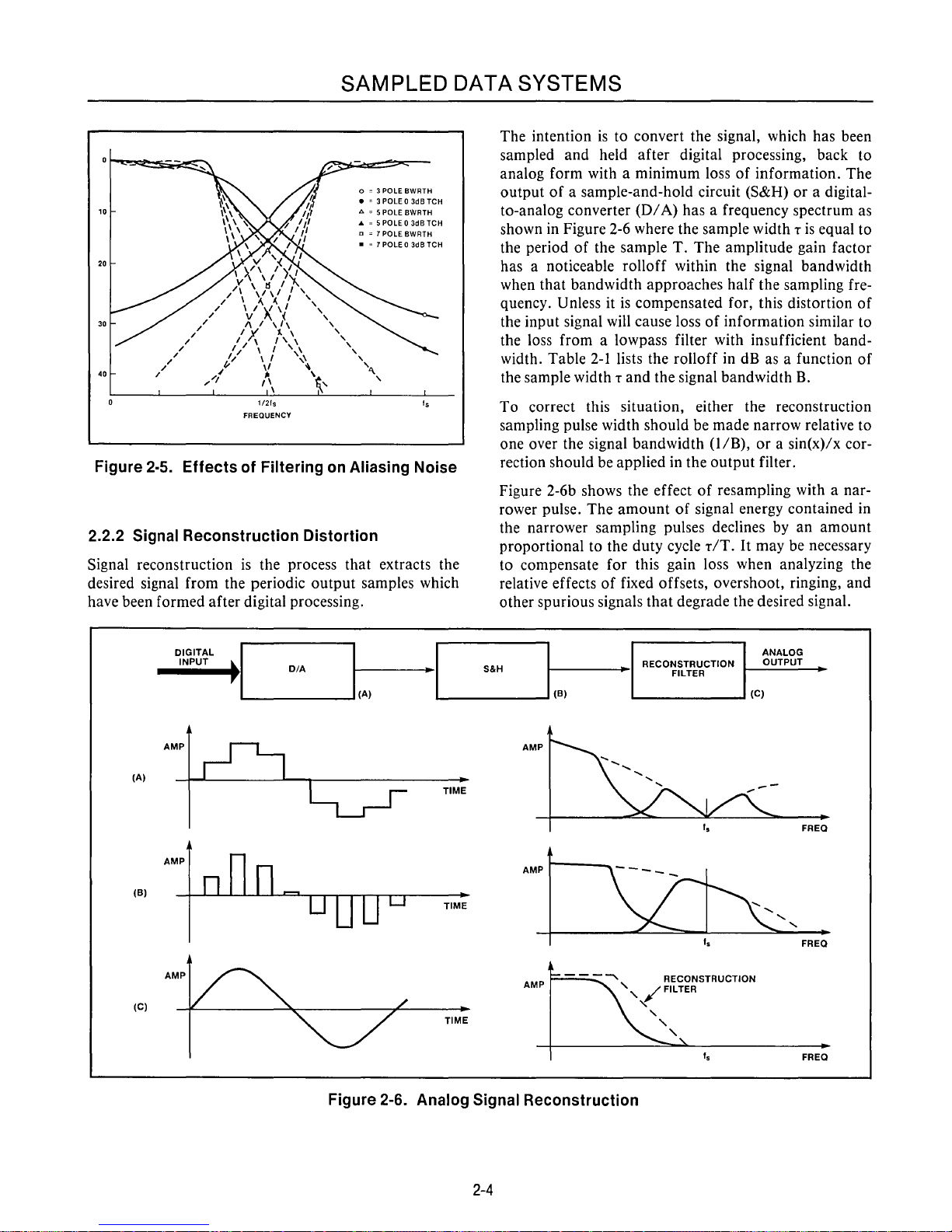
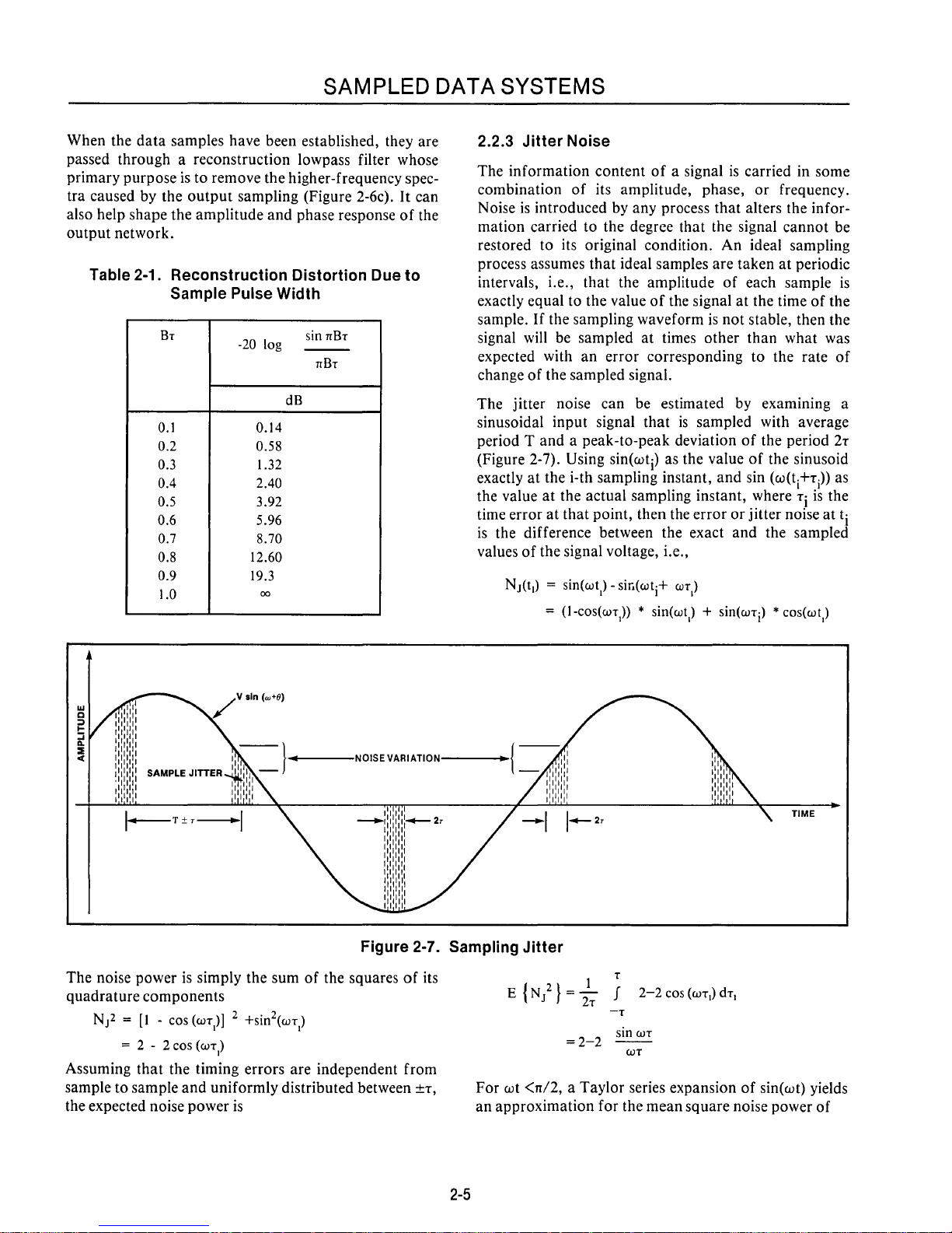
2.2.2
Signal Reconstruction Distortion
Signal reconstruction
is
the process
that
extracts the
desired signal from the periodic
output
samples which
have been formed
after
digital processing.
DIGITAL
INPUT
D/A
The intention
is
to
convert the signal, which has been
sampled
and
held
after
digital processing, back
to
analog form with a
minimum
loss
of
information.
The
output
of
a sample-and-hold circuit (S&H)
or
a digital-
to-analog converter (DI A) has a frequency spectrum as
shown in Figure 2-6 where the sample width
T
is
equal to
the period
of
the sample
T.
The
amplitude
gain factor
has a noticeable
rolloff
within the signal bandwidth
when
that
bandwidth
approaches
half
the sampling fre-
quency. Unless it
is
compensated for, this distortion
of
the input signal will cause loss
of
information
similar to
the loss
from
a lowpass filter with insufficient band-
width. Table
2-1
lists the
rolloff
in dB as a function
of
the sample width T
and
the signal
bandwidth
B.
To
correct this situation, either the reconstruction
sampling pulse width should be
made
narrow
relative
to
one over the signal
bandwidth
(1/B),
or
a sin(x)/x cor-
rection should be applied in the
output
filter.
Figure 2-6b shows the effect
of
resampling with a nar-
rower pulse.
The
amount
of
signal energy contained in
the narrower sampling pulses declines by
an
amount
proportional
to the
duty
cycle TIT.
It
may
be necessary
to
compensate for this gain loss when analyzing the
relative effects
of
fixed offsets, overshoot, ringing, and
other spurious signals
that
degrade the desired signal.
ANALOG
OUTPUT
·1
L
S&H
~
___
----I,",~I
RECO~~L~~~CTION
'-
_____
-"
(8)
""--
_____
....
(C)
.;
(A)
AM'I~
LLJ
..
TIME
AMP
I.
FREO
AM'I
n
n
Dr-.
(8)
DODD
TIME
AM'
t
~"
I.
FREO
AM'p~//
(C)
-------
RECONSTRUCTION
AMP
,
,/FILTER
,
"
"
I.
FREO
..
TIME
Figure 2-6. Analog Signal Reconstruction
2-4
Page 20
SAMPLED DATA SYSTEMS
When the
data
samples have been established, they are
passed through a reconstruction lowpass filter whose
primary
purpose
is
to remove
the
higher-frequency spec-
tra caused by the
output
sampling (Figure 2-6c).
It
can
also help shape the
amplitude
and
phase response
of
the
output
network.
Table 2-1. Reconstruction Distortion Due to
Sample Pulse Width
BT
-20
log
sin
nBT
---
nBT
dB
0.1
0.14
0.2 0.58
0.3
1.32
0.4
2.40
0.5
3.92
0.6 5.96
0.7 8.70
0.8 12.60
0.9
19.3
1.0
00
2.2.3 Jitter Noise
The
information
content
of
a signal
is
carried in some
combination
of
its amplitude, phase,
or
frequency.
Noise
is
introduced by any process
that
alters the infor-
mation
carried to the degree that the signal
cannot
be
restored to its original condition.
An
ideal sampling
process assumes
that
ideal samples are
taken
at
periodic
intervals, i.e.,
that
the amplitude
of
each sample
is
exactly equal to the value
of
the signal
at
the time
of
the
sample.
If
the sampling waveform
is
not
stable, then the
signal will be sampled
at
times
other
than
what
was
expected with
an
error
corresponding
to
the rate
of
change
of
the sampled signal.
The
jitter noise can be estimated by examining a
sinusoidal
input
signal
that
is
sampled with average
period T
and
a peak-to-peak deviation
of
the period
2T
(Figure 2-7). Using sin(wti) as the value
of
the sinusoid
exactly
at
the i-th sampling instant,
and
sin
(W(tj+T
j
» as
the value
at
the actual sampling instant, where
Ti
is
the
time
error
at
that
point, then the
error
or
jitter noise
at
ti
is
the difference between the exact
and
the sampled
values
of
the signal voltage, i.e.,
NJ(t.) = sin(wt
l
) -
sir,(wti+
WT
I
)
=
(l-COS(WT)
* sin(wt) + sin(wTi) * cos(wt)
11--
}
....
I-----NOISE
VARIATION---
__
SAMPLE
JITTER~::II
-
11111111
11111111
I-T±T_/
/_2T
TIME
Figure 2-7. Sampling Jitter
The noise power
is
simply the sum
of
the squares
of
its
quadrature
components
NJ2 =
[1
- cos
(WT)]
2 +sin2(WT)
= 2 -
2COS(WT
I
)
Assuming
that
the timing
errors
are independent from
sample
to
sample
and
uniformly distributed between
±T,
the expected noise power
is
2-5
T
E {N/ } =
;T
f
2-2
cos
(WT
I
)
dTI
=2-2
sin
WT
WT
For
wt
<TI12,
a
Taylor
series expansion
of
sin(wt) yields
an
approximation
for the
mean
square
noise power
of
Page 21

SAM PLED DATA SYSTEMS
The
signal-to-noise ratio (SNR)
of
a sampled sinusoid
sin(wT) due
to
jitter uniformly distributed over
-T~TO~T
seconds
is
Mean
Square
Signal
Mean
Square
Noise = (SNR)
jitter
3
(WT)
2
2
Expressed
another
way,
(SNR) .. = 0.038
(~)2
JItter T
where T
is
the
period
of
the sampled signal. The jitter
SNR
is
plotted in Figure 2-8 as a function
of
the jitter-
tolerance
ratio
T/T.
rg
-'UI
<tUl
z-
,,0
iii
Z
WUl
a:
a::
<t<
::J:l
0°
cn
Ul
ZZ
<t<
wUl
::;:i:
a:
z
III
I
r
LOG SCALE
IlJ..U..l.LL..J
"-
10 5 2 1
100
~
~
80
60
40
20
o
10-6
~
~
""
~
10-
5
10-
3
JITTER TOLERANCE, T
MINIMUM SIGNAL PERIOD, T
Figure
2-8.
Jitter
SNR
""
Since each pass
of
the 2920
program
uses the same
number
of
clock cycles, overall sampling jitter will be
entirely a function
of
the clock stability.
When
the
2920
clock
is
crystal controlled,
clock/sampling
jitter will be
insignificant.
2-6
2.2.4 Quantization Noise
Digital signal processing
of
a signal implies
that
at
specific times the signal
is
sampled
and
a digital word
is
formed
that
represents
the
amplitude
of
the signal
at
that
time.
The
sections above described the effect
of
this
sampling process,
and
showed
that
a minimum loss
of
information
is
possible with the
proper
selection
of
the
input filter
and
sampling frequency.
The conversion
from
a continuous signal
to
a digital
signal requires
that
signal voltage be divided into a finite
number
of
levels which can be defined using a digital
word n bits long.
An
n-bit word can describe 2n different voltage steps. Signal variations between these
steps will go undetected.
It
is
therefore necessary
to
determine the range
of
signal levels from maximum
to
minimum
that
the system must
operate
with, to deter-
mine the
number
of
bits needed in
an
A/D
conversion.
Figure 2-9 illustrates how
the
error
voltage (called
quan-
tization noise)
is
generated. The corresponding ratio
of
peak signal to
quantization
noise, expressed in dB,
is
a
function
of
the digital
word
length.
OUTPUT
VOLTAGE
Ja
=
2N-1
N = It BITS
Ja
' 6N OB I
MAX
I
ERROR I
1
:
VOLTAGE"
"
t\
" 1\
t\
I
'J 'J
\I
\I
\I
'\
INPUT
VOLTAGE
INPUT
VOLTAGE
2 3 4 5 6 7 8
91011
SINO
DB
"6
18 24 30 36 42 48 54 60 66
Figure 2-9. Quantization Noise
The
quantizing
error
can be expressed in terms
of
the
total
mean
squared
error
voltage between the exact
and
the quantized samples
of
the signal. In Figure 2-10,
any
signal voltage v(t) falls between the i-th
and
the (i+ 1
)th
levels which define the i-th quantizing interval.
The
error signal
ei
is
expressed
as
ei=V(t)-Vi
Page 22
where
SAMPLED
DATA
SYSTEMS
ei =
error
voltage between
the
exact
and
the i
th
quantized
voltage levels
V(t)
=
input
signal voltage
Vi
= voltage
of
the i
th
quantized
interval
Figure 2-10. Quantization Step
2-7
Assuming
uniform
quantization
and a uniform
distribu-
tion
of
the
signal voltage, the resulting signal-to-
quantization-noise
ratio
is
S/N
q
=
M2-1
or,
represented
as a logarithm,
S/N
q
= (6)*(n) dB,
n>2
where
S
is
the
peak
signal
power
Nq is
the
mean
quantization
noise
M
is
the
number
of
quantization
levels = 2
n
n
is
the
number
of
bits in the
amplitude
word
The
2920
has a programmable
AID
conversion
of
up
to
9 bits
of
resolution,
giving the device
up
to
54dB
of
instantaneous
dynamic
range
based
on
quantization
noise
alone.
For
systems where the
total
dynamic
range
is >54dB
but
the
instantaneous
requirements
are
within
this range,
approaches
such as
automatic
gain
control,
variable
attenuators,
or
programmable
amplifiers
can
be used in
conjunction
with the 2920.
Some
of
these
approaches
are
discussed in
Chapters 4 and
7.
Page 23

Page 24
The 2920
Signal
Processor
3
Page 25

Page 26
CHAPTER 3
THE
2920
SIGNAL PROCESSOR
3.0 THE 2920 SIG NAL PROCESSOR
This chapter will discuss the 2920 device operation functional elements
and
operating conventions.
3.1
Device Operation
3.1.1 Overview of the 2920
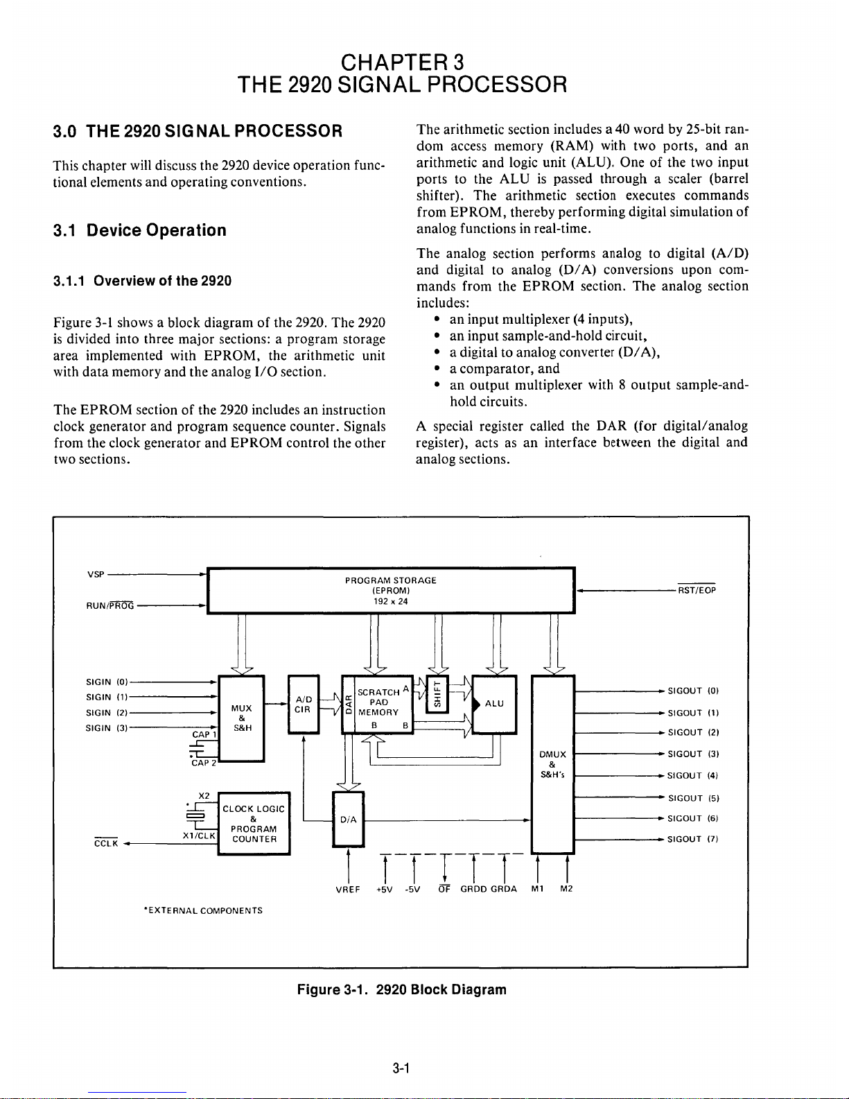
Figure
3-1
shows a block diagram
of
the 2920. The 2920
is
divided into three
major
sections: a program storage
area implemented with
EPROM,
the arithmetic unit
with
data
memory
and
the analog 110 section.
The
EPROM
section
of
the 2920 includes
an
instruction
clock generator
and
program sequence counter. Signals
from the clock generator
and
EPROM
control the other
two sections.
The
arithmetic section includes a 40 word by 25-bit ran-
dom
access memory (RAM) with two ports,
and
an
arithmetic
and
logic unit (ALU). One
of
the two input
ports to the
AL U is
passed through a scaler (barrel
shifter).
The
arithmetic section executes commands
from
EPROM,
thereby performing digital simulation
of
analog functions in real-time.
The
analog section performs analog to digital
(AID)
and
digital to analog
(01
A) conversions
upon
com-
mands from the
EPROM
section.
The
analog section
includes:
•
an
input multiplexer
(4
inputs),
•
an
input sample-and-hold circuit,
• a digital to analog converter
(01
A),
• a
comparator,
and
•
an
output
mUltiplexer with 8
output
sample-and-
hold circuits.
A special register called the DAR (for digital/analog
register), acts as
an
interface between the digital and
analog sections.
VSP------------~--------------------------------------------,
PROGRAM STORAGE
(EPROM)
1----------
RST/EOP
RUN/PROG--------·L
__
~~--------------~'9:2~X~24~--~----~~----~~
SIGIN
(0)----------,
SIGIN
(1)-------1
SIGIN
(2)-------,
SIGIN
(3)------1
X2
CCLK
_----X-'_/C_LK-I
CLOCK LOGIC
&
PROGRAM
COUNTER
'EXTERNAL
COMPONENTS
1
VREF
Figure 3-1. 2920 Block Diagram
3-1
1------
SIGOUT
(0)
1--------
SIGOUT
(,)
1-------
SIGOUT
(2)
DMUX
1--------
SIGOUT
(3)
&
s&H's
1--------_
SIGOUT
(4)
1------
SIGOUT
(5)
1--------
SIGOUT (6)
I------SIGOUT
(7)
M2
Page 27
THE
2920
SIGNAL PROCESSOR
3.1.2 Analog Operations
The basic operation
of
the 2920 can be seen by assuming
that an input signal
is
to be processed, for example by a
digital filter,
and
outputted
as
an
analog signal. Under
program control, one
input
would be selected from the
four possible inputs,
and
the signal sampled
and
held.
This signal would then be converted to a digital word
with up
to
9 bits
of
linear conversion (sign bit
and
8
amplitude bits).
The bits are formed by a successive approximation
AID
conversion
and
stored in the DAR. This DAR register
is
the interface between the analog
and
digital sections
of
the 2920. During
AID
conversion, the DAR accum-
ulates each bit
of
the digital word until conversion
is
complete.
This word may then be loaded into a scratch pad RAM
location for further processing. When outputting a
value, the 9 most significant bits
of
a RAM location are
loaded into the DAR. Under program control, the DAR
drives the
01
A converter, whose
output
can be routed
to any
of
8 analog outputs by the
output
demultiplexer
and
S&Hs.
3.1.3 Digital Operations
The digital
part
of
the 2920 will be operating
simultaneously with the above analog operations.
For
example, during a 9-bit
AID
conversion, a 3-pole
lowpass filter could be realized using the digital cir-
cuitry. The digital loop includes the 2-port addressable
40-word RAM, a binary shifter,
and
the ALU. Under
program control, two 25-bit locations in RAM are
simultaneously addressed, with the
data
from the A
address passing through the binary shifter. This shifter
allows scaling from 22 (a 2-bit left shift) to
2-
13
(a 13-bit
right shift). The scaled A value
and
the unscaled B value
are then propagated to the
ALU
as operands.
The
ALU operates
on
these values with digital instruc-
tions specified by the
program.
The
25-bit result
of
that
operation
is
loaded into the B address location
of
the
RAM.
What
makes the 2920 fast enough for real-time
processing
is
that
the entire set
of
actions (analog opera-
tion, dual memory fetch, binary shift,
ALU
execution,
and
write back to RAM can take place in as little as 400
nanoseconds (depending
on
the clock rate).
3-2
3.2 A Closer Look at the Functional
Elements
3.2.1 EPROM Section
The
EPROM
section contains 4608 bits
of
user pro-
grammable
and
erasable read-only memory. In normal
operation
of
the 2920, i.e., in the RUN mode, it
is
arranged as
192
words
of
24
bits each. Each word corresponds to one 2920 instruction. During programming,
each 24-bit word
is
treated as six 4-bit nibbles; i.e., in
PROGRAM
mode the
EPROM
appears as 1152 words
of
four bits each. Figure 3-2 shows the 2920 pin connec-
tions for the RUN and
PROG
mode.
Run
Mode-During
the RUN
mode
the
EPROM
section acts as the system controller. Each 24-bit control
word contains bit patterns that determine the operations
to be performed by the analog
and
arithmetic sections.
The control word
is
composed
of
five fields,
of
which
one controls the analog section
and
the remaining four
control the arithmetic section.
The
four arithmetic sec-
tion control fields include the two 6-bit fields which
identifies RAM locations, a 4-bit scaler control field
and
a 3-bit ALU control field.
In the RUN mode,
EPROM
word addresses
are
numbered from 0 to 191. In
normal
operation
allioca-
tions are accessed in sequence
and
no program jumps
are allowed.
The
EPROM
program
counter returns to
location
0
upon
completion
of
execution
of
the com-
mand in word 191,
or
when
an
EOP
instruction
is
encountered in the analog control instruction field.
The
EOP
feature allows the
program
to be terminated at the
end
of
a user's program shorter
than
192
words. Place-
ment
of
the
EOP
is
explained below.
The
EPROM
may
be
thought
of
as a crystal-
or
clock-
controlled cycle generator as
program
length determines
the sampling frequency
of
the analog signals.
If
an
input
is
sampled once per
program
pass, the sampling fre-
quency
is
liNT
where N
is
the number
of
words
(instructions) in the program
and T is
the time required
to execute one instruction.
The
EPROM
fetchlexecute cycle
is
pipelined four deep,
meaning
that
the next four instructions are being
fetched while the previously fetched instructions are
being executed. Although otherwise invisible to the
user, this technique requires
that
the
EOP
instruction be
inserted in a word with an address divisible by four,
Page 28
THE
2920
SIGNAL
PROCESSOR
e.g., program location
0,4,
....
,188.
The
EOP
does
not
take effect until the three following instructions are
executed.
An
open
drain active low logic pin RST may be used to
display the presence
of
an
EOP
signal
or
to apply an
external active-low reset signal (which forces a
jump
to
EPROM
location zero). This
output
can sink 2.5mA,
which allows connecting
a 2.2K pull-up resistor,
or
one
TTL
load
with a 6.2K pull-up.
If
the internal
EOP
instruction
is
not
used, the pin may be tied to VCC
or
driven by a
TTL
or
CMOS gate.
An
OR-tied connection
may also be used. In normal operation, the 2920 does
not use a reset signal,
but
one may be useful in
applications requiring synchronization
of
the 2920
and
other equipment.
Proper
operation
of
the
EOP
instruc-
tion requires-
an
external pull-up resistor
on
the RST
pin.
Since RST
and
EOP
are internally equivalent functions,
an externally generated RST must
conform
to the same
rules as the
program
placement
of
EOP.
CCLK pro-
vides this cycle indication
and
should be used to strobe
an externally supplied RST signal.
Two pins associated with the
PROGRAM/RUN
mode
selection are
VSP
and
RUN/PROG.
Both pins should
be tied to
GRDD
(digital ground) for RUN mode.
EPROM
Program
Mode-During
programming,
each 24-bit
EPROM
word
is
treated as six 4-bit nibbles,
with the result
that
the
EPROM
is
programmed as if it
were organized as 1152 x 4. Table
3-1
shows the rela-
tionship between the control fields
and
the bit positions
in each nibble. (See the sections below
on
the arithmetic
and
analog sections for details
on
the significance
of
each control bit.)
Many
of
the pins
of
the 2920
perform
different func-
tions in the
PROG
mode
than
they
do
in the RUN
mode. These differences are noted in Figure 3-2.
Note
that
for the 2920 pin outs as shown in Figure 3-2,
the power supply conventions are different for RUN
and
PROG
mode. These conventions allow the pro-
grammer designer to use
popular
TTL
family products
as a basis for design.
With
the exception
of
the power
connections, VSP
is
the only pin
that
requires other
than
5 volt logic levels.
3-3
In the
PROG
mode, the four pins labelled
DO
through
D3
are used for
both
data
input
and
output.
Their direc-
tion
is
controlled by the
PROG/VER
pin. A high level
on
this pin switches to
input
mode, a low to
output.
This
feature allows the programmed
data
to be verified
before proceeding to the next address. The
input
data
must be presented in true form (logical 1 =high, logical
O=low)
but
is
read back complemented (logical 1 =low,
10gicaI0=high).
The
internal counters are incremented during the falling
edge
of
INCR. 1152
INCR
transitions will complete the
full
program
cycle.
To
initialize at nibble address 0,
RST must be pulsed active (low)
and
an
INCR
must be
issued.
For
programming the
RUN/PROG
pin
must
be tied to
VBB, the VCC pin to +5 volts,
and
VSP (the high
voltage programming pin) should be pulsed from
5.0 ±
.5
volts to +25 ± 1 V @ 15mA max.
The
data
pins
DO
through
D3
have open drains
in
the
output
direction;
thus pull up resistors are required.
Table
3-1.
2920
Control
Bit
Assignments/Programming
Nibble
Bit
Assignment
Nibble
Number
MSB LSB
(3) (2)
(1
) (0)
0
ADFO
ADK2
ADKI
ADKO
1
A2
Bl
Al
ADFI
2
A4
B3
A3
B2
3
AO
B5
A5
B4
4
S2
Sl
SO
BO
5
L2
Ll
LO
S3
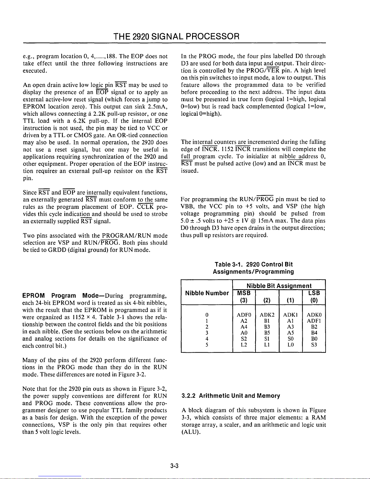
3.2.2
Arithmetic
Unit
and
Memory
A block diagram
of
this subsystem is shown in Figure
3-3, which consists
of
three
major
elements: a RAM
storage array, a scaler,
and
an
arithmetic
and
logic unit
(ALU).
Page 29

TH E
2920
SIGNAL
PROCESSOR
PIN
DESCRIPTIONS
(RUN
MODE)
Symbol
Function
SIGOUT
8
PinS
corresponding
to the 8
demultl-
plexed analog
outputs
(0-7)
GROA
Analog signal
ground
held at
or
near
GROO tYPically
CAP,
& CAP2
External
capacitor
connections
for
the
Input
signal sample and
hold
CirCUit
VREF
Input
Reference Voltage
SIGIN
4 pins
corresponding
to the 4
multi-
plexed analog Inputs (0-3)
VBB
Most
negative
power
Pin set at -5 volts
dUring run mode
(different
voltage
In
program
mode)
X1/CLK
Clock
Input
when uSing external
clock
signals,
OSCillator
Input
for
external
crystal when uSing Internal
clock
X2
OSCillator
Input
for
external crystal when
uSing Internal
clock
GROO Digital
ground
Vee
5 volts In run mode
CCLK
Internal
fetch
cycle clock
output
The
failing
edge
designates
the
START
of
a
new
PROM
fetch
cycle.
CCLK
IS
1/16
of
X1/CLK rate.
RUN/PROG
Mode
control
tied
to
GROO In run mode
(different
voltage
In
program
mode)
RST/EOP
Low
RST
input
initializes
program
fetch
counter
to
first
location.
As an
output
It
Signifies
EOP
instruction
present (open
drain,
active
low).
PIN
DESCRIPTIONS
(PROGRAM
MODE)
Symbol
00,01,02,03
Function
4
pins
carrying EPROM program
data
for
both
input
and
output
(open drain, active
low
output;
active
high
Input)
VB"
VB2
VB3
Digital
ground
In
PROGRAM mode
(dif-
ferent voltage for RUN mode)
VS"
VS2,
VS3
+5 volts In
PROGRAM
mode
(function
changes
for
RUN
mode)
RUN/PROG
Mode
control
pin tied to
VBB
for
PROGRAM
mode (voltage
changes
for
RUN
mode)
INCR
Input
pulse Increments the
nibble
(4-blts)
counter
In PROG
mode
(func-
tion
changes
In
RUN
mode)
VSP
PROGIVER
EPROM po\',er pin
+5
volts
for
VERIFY
mode and +25 volts
for
PROGRAM
mode
(different
voltage In RUN
mode)
Controls
EPROM
bl-dlrectlonal
data bus
for
venfy
(low)
or
program
(high)
Input
pulse resets
nibble
counter
to
POSition zero
for
start
of
programming
Symbol
OF
VSP
M1, M2
Function
Indicates
an
overflow
In the
current
ALU
operation
(open drain, active
low)
EPROM
power
Pin 0 volts
for
RUN
mode
(Different
voltage In
program
mode)
Two
pins
which
specify
the
output
mode
of
the
SIGOUT
pins (see Table 4)
SIGOUT 3
SIGOUT
2
SIGOUT 4
SIGOUT 1
SIGOUT 5 SIGOUT 0
GROA
M1
SIGOUT 6
M2
SIGOUT 7
VSP
CAP,
OF
VREF
RST/EOP
CAP
2
RUN/PROG
SIGIN 0
CClK
SIGIN 3
Vee
V
BB
GROO
SIGIN
2
X
2
SIGIN 1
XI/ClK
Run Mode
Pin
Configuration.
03
02
01
00
VSl
PROG/VER
VSP
INCR
RST
RUN/PROG
Program Mode
Pin
Configuration.
Figure 3-2. 2920
Pin
Descriptions
3-4
Page 30
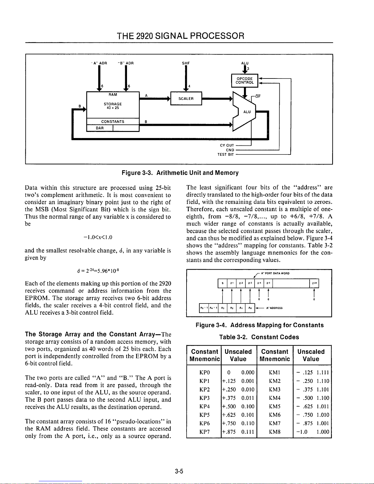
THE
2920
SIGNAL
PROCESSOR
'A"
ADR
"B"
ADR
RAM
STORAGE
40 x 25
CONSTANTS
DAR
SHF ALU
A
CY OUT
CND
_____
--J
TEST BIT
---------1
Figure
3-3.
Arithmetic
Unit
and
Memory
Data
within this structure are processed using 25-bit
two's complement arithmetic. It
is
most convenient to
consider an imaginary binary point
just
to the right
of
the MSB (Most Significant Bit) which
is
the sign bit.
Thus the normal range
of
any variable x
is
considered to
be
-1.0<x<1.0
and
the smallest resolvable change,
d,
in any variable
is
given by
d =
2-24=5.96*10-
8
Each
of
the elements making
up
this
portion
of
the 2920
receives
command
or
address
information
from the
EPROM.
The
storage array receives two 6-bit address
fields, the scaler receives a 4-bit control field,
and
the
ALU receives a 3-bit control field.
The
Storage
Array
and
the
Constant
Array-The
storage array consists
of a random
access memory, with
two ports, organized as 40 words
of
25
bits each. Each
port
is
independently controlled from the
EPROM
by a
6-bit control field.
The two ports are called
"A"
and
"B."
The A
port
is
read-only.
Data
read from it are passed, through the
scaler, to one input
of
the
ALU,
as the source operand.
The B
port
passes
data
to the second
ALU
input, and
receives the
ALU
results, as the destination operand.
The constant
array
consists
of
16
"pseudo-locations"
in
the RAM address field. These constants are accessed
only from the A
port,
i.e., only as a source
operand.
3-5
The least significant
four
bits
of
the
"address"
are
directly translated to the high-order four bits
of
the
data
field, with the remaining
data
bits equivalent to zeroes.
Therefore, each unsealed constant
is
a multiple
of
one-
eighth, from
-8/8,
-718,00',
up
to
+6/8, +7/8.
A
much wider range
of
constants
is
actually available,
because the selected constant passes
through
the scaler,
and can thus be modified as explained below. Figure 3-4
shows the
"address"
mapping for constants. Table 3-2
shows the assembly language mnemonics for the constants
and
the corresponding values.
~
A"
PORT DATA WORD
1 1
II!
!
lAS
+.
-11
A, I A, I A, I Ao
1-
A"ADDRESS
Figure
3-4.
Address
Mapping
for
Constants
Table
3-2.
Constant
Codes
Constant
Unscaled
Constant
Unscaled
Mnemonic
Value
Mnemonic
Value
KPO
0 0.000
KMI - .125
1.111
KPI
+.125 0.001 KM2
- .250
1.110
KP2
+.250
0.010
KM3
- .375 1.101
KP3
+.375 0.011 KM4 - .500
1.100
KP4 +.500 0.100
KM5
- .625
1.011
KP5
+.625 0.101 KM6 - .750
1.010
KP6
+.750
0.110
KM7
- .875
1.001
KP7
+.875 0.111 KM8
-1.0
1.000
Page 31

THE
2920
SIGNAL
PROCESSOR
The
DAR
can be used as a source
or
a destination
operand.
It
is
both
a digital
to
analog register
and
an
analog
to digital register.
It
is
nine bits wide, occupying
the nine
most
significant bit positions
of
a word whose
other bits are set
to
ones in
order
to
correct for
AID
conversion
number
system offset when read into the
processor.
The
DAR
output
is
also tied directly
to
the digital to
analog converter
(DI A) inputs.
The
DAR
is
used as a
successive-approximation register for
analog
to digital
conversion,
under
control
of
the analog function
instruction field.
Each
bit position
of
the
DAR
can also
be tested by the
ALU
for conditional arithmetic
operations.
Table
3-3.
Scaler
Codes
and
Operations
Scaler
Bit
Equivalent
Code
Values
Multiplier
Operation
L02
1110
22=
4.0
"A"x22
LOI
1101
2'=
2.0
"A"x21
ROO
1111
2°= 1.0
"A"x2°
ROI
0000
2-1=0.5
"A"x2-
1
R02
0001
2-
2
=
0.25
R03
0010
2-
3
=
0.125
R04
0011
2-4= 0.0625
"A"x2-
4
R05
0100
2-5= 0.03125
Scaler-
The
scaler
is
an
arithmetic barrel shifter
located between the A
port
of
the
RAM
and the
ALU.
Values read from the A
port
can be shifted left
or
right.
The
shifts can be a
maximum
of
two positions to the left
or
a maximum
of
thirteen positions right. Left shifts fill
with zeroes
at
the right; right shifts fill with the sign bit
at the left.
As explained above, these arithmetic shifts are
equivalent to multiplication
of
the A
port
value by a
power of two, where the
number
of
positions shifted
is
the 2' s power.
The
scaler
is
controlled by a 4-bit wide control field
from the
EPROM,
as shown in Table 3-3.
Note
that
left
shifts may
produce
numbers which are too large to fit
within a 25-bit field.
The
handling
of
such large
numbers
is
described in the
ALU
section below.
The
ALU-
The
Arithmetic Logic
Unit
calculates a
25-bit result
from
its A
and B operands
(source
and
destination) based
on
an
operation
code from the
EPROM.
The
25-bit result
is
written back into the B
(destination) memory location
at
the end
of
the
instruction cycle.
One
condition for overflow
is
a left shift where the sense
of
the sign bit changes.
For
this reason the
ALU
uses
extended precision
to
allow calculation
of
the correct
3-6
Scaler
Bit
Equivalent
Code
Values
Multiplier
R06
0101
26= 0.015625
R07
0110
27= 0.0078125
R08 0111
28= 0.00390625
R09 1000
2-9= 0.001953125
RIO
1001
2-1°=
0.0009765625
Rll
1010
2-
11
= 0.00048828125
R12
1011
212=0.000244140625
R13
1100
2 -13=0.0001220703125
result even when receiving left-shifted operands from
the scaler.
If
the
computed
result
YY
exceeds the
bounds
-l.O~YY<l.O
an
overflow condition is indicated.
When
overflow
limiting
is
enabled, this condition causes the result to
be
replaced with the legal value closest
to
the desired result,
i.e., with
-1
if the
computed
value was negative,
and
with + 1.0 if
the
result was positive.
In binary these extreme values
appear
as
Binary
Value
1000 000
000
000
000 000 000 000
-1.0
0111
111
111
111
111
111
111
111
1-2-
24
respectively.
This
overflow
saturation
characteristic
is
useful for realizing certain non-linear functions such as
limiters,
and
is
beneficial to the stability
of
filters.
The
OF
pin indicates
that
an
overflow
is
occurred
on
the
previous
operation
(cycle). This
output
is
active low
and
open-drain. In the case where overflow
is
not
enabled,
each binary
number
is
extended
to
28-bit precision by
extending the sign bit
to
the left.
The
calculation
is
done
a!1d
the low
25
bits are written
back
to
the destination.
Page 32

THE
2920
SIGNAL PROCESSOR
The
operations
performed
by the
ALU
are summarized
in
Table
3-5. Although
most
of
them are self-
explanatory, the following details may be useful
at
this
point.
Absolute value (ABS)
and
absolute
add
(ABA) convert
the"
A"
operand
(source) to its absolute value before
performing
any calculations.
Load
A (LOA)
and
ABS
are treated as arithmetic operations by the
ALU,
mean-
ing
that
the source
is
added
to zero
and
then replaces the
"B"
operand
(destination). This causes the correct han-
dling
of
those overflows caused by left shift operations.
The
operation
LIM sets the result to positive
or
negative
full scale, based
on
the
"A"
port
sign bit, behaving
much like a forced overflow. However, the overflow
flag will not indicate overflow for a LIM unless the
given source
operand
and
shiftcode would produce
an
overflow in
an
LOA
operation.
The
constant
source codes allow you to select constants
for arithmetic operations.
The
procedure
is
described in
the section
on
the storage
array
of
the ALU
and
memory. Table 3-2 above lists the mnemonics and corresponding un scaled value
of
each
constant.
Each value
is
passed
through
the scaler,
and
so
may
be multiplied
by a value
2k,
where k runs from
+2
to
-13.
The scaler
codes
and
equivalent multiplier values are shown in
Table 3-3.
Conditional Arithmetic
Operations-In
addition to
the basic operations described in Table 3-5, some
ALU
functions
may
execute conditionally. Certain codes in
the
analogi
digital control field cause the execution
of
the arithmetic
operation
to be conditional
on
a selected
bit
of
the
DAR.
The
conditional instructions are
tabulated in Table 3-5b.
The
conditional field
code
selects a bit
of
the DAR,
and
uses its value
to
determine how the instruction
is
to be
executed. A
"I"
implies execution
of
the instruction; a
"0"
implies execution
of a NOP.
For
conditional sub-
tract, the bit actually used
is
the carry
from
the previous
result. In this case the selected bit
of
the
DAR
is
set
equal
to
the carry
from
the
current
instruction.
Conditional
additions are used to mUltiply one variable
by a second, as discussed in
Chapter
4.
The
mUltiplier
is
loaded into the
DAR,
and
the multiplicand
is
added
conditionally
to
the partial
product.
3-7
Conditional
subtraction
is
used to divide
one
positive
variable by
another,
using a non-restoring division
algorithm.
The
divisor
is
conditionally subtracted from
the dividend,
and
quotient
bits are assembled in the
DAR.
Conditional operations may also be useful for performing logic, also shown in
Chapter
4.
Table 3-4 sum-
marizes the properties
of
the arithmetic section.
Table 3-4.
Memory-ALU
Section Summary
ALU result bit width
Number System
Operand
A
ALU instruction field
width
Scaler instruction field
width
"A"
and
"B"
port
address field width
Ancillary Instructions
25
bits
2's
complement
Read Only Memory
Port
A,
Scaled by shifter,
28
bits wide
Read
Port
B, Unsealed,
25
bits
expanded to 28 bit equivalent
3 bits
4 bits
6 bits each
ConditIonal
arithmetic,
op
codes are
part
of
analog control
field
Available Storage
"A"
port, AdrO-39, Read Only,
Locations
25
bits.
"B"
port,
AdrO-39,
Read-Write
25
bits.
Digital-Analog-Register
"A"
port, Adr40, Read Only, 9
MSBs,
16
LSB's are filled with
Is.
"B"
port,
same as
"A"
port
but
read-write.
Constant
Register
"A"
port
only, low 4 bits
of
adr.
Field placed in 4 MSB's
of
25-bit width. Low
21
LSB's fill
as O's.
Scaler Range
22
(left
2)
to
TlJ
(nght
13).
3.2.3 The Analog Section
Figure 3-5 shows a detailed block diagram
of
the 2920's
analog section, which provides four analog
input
chan-
nels
and
eight analog
output
channels.
It
includes
circuitry for analog-to-digital conversion by successive
approximation,
and
the sample-and-holds for
both
inputs
and
outputs.
Page 33

THE
2920
SIGNAL
PROCESSOR
Table 3-5.
Memory-ALU
Instruction Opcodes
a.
Non-Conditional Arithmetic
ALU
MNEM Operation*
210
000
XOR
BED(A·
2k)
....
B
001
AND
BA(A·2k)
....
B
010
LIM
+ 1
**
....
B if A ~ 0
-1
....
Bif
A<O
o 1 1 ABS
0+ I A·2
k
I
....
B
I 0 0
ABA
B+ I
A·2
k
I
....
B
I 0 1 SUB
B-
(A·2k)
....
B
I 1 0
ADD
B+
(A·2k)
....
B
I 1 1
LDA
0+
(A·2k)
....
B
*Note-k
is
the value selected by the shift code,
-13 ~ k ~ + 2
*
*Note-the
largest positive value
(1-2-
24
)
is
stored.
b. Conditional Arithmetic Operations
Description/Comments
Sign
of
A saturates
output
Absolute Value
Absolute Value
and
Add
ALU
Functions
made
Conditional
by selected codes in the Analog
Control
Field.
ALU
Function Bit Tested IF Tested Bit = 0 IF Tested Bit = 1
ADD
(110)
DAR
(n) NO-OP(B+O
....
B)
ADD
(B+A·
2k ....
B)
LDA(lll)
DAR
(n)
NO-OP(B+O
....
B)
LDA
(O+A· 2k ....
B)
SUB (101)
PREV
cy
ADD(B+A·2k ....
B)
SUB (B-A· 2k
....
B)
cy
....
DAR(n) cy
....
DAR(n)
Note-
DAR(n) represents a bit
of
the
DAR,
as selected by the conditional
operand
in the analog
control
field.
For
ADD
and
LDA, the selected bit
is
tested.
For
SUB, the selected bit
is
altered by being set to the carry
output
of
the highest
order
position
of
the
ALU;
and
the conditional operation
is
base,d
on
a test
of
the carry resulting
from
the previous
ALU
operation.
For
SUB with
CNDS,
CY
is
set
to
the
DAR.
c. Overflow Manipulation Operations
ALU
Function
ABA
XOR
"Don't
Care"
AD
Function
CND(K)
CND(K)
EOP
3-8
Description
Disable Overflow
Enable Overflow
Enable Overflow
Page 34

THE
2920
SIGNAL
PROCESSOR
SIGINO
SIGINl
SIGIN2
SIGIN3
FROM PROM
110
CAPl
CAP2 AGND
CND TEST BIT
SIGOUTO
SIGOUT1
SIGOUT2
SIGOUT3
SIGOUT4
SIGOUT5
SIGOUT6
SIGOUT7
VREF
Figure 3-5. Analog Section Block Diagram
All operations
of
this section are controlled by a five-bit
control field.
It
can be divided into two subfields: a two-
bit function selector
and
a three-bit modifier field.
Table 3-6 summarizes the analog section operations.
Giving the most significant bits first, the function select
bits are designated ADF1
and
ADFO; the modifier bits
are ADK2, ADK1,
and
ADKO.
The
basis
analog functions are as follows:
Execution
of
one
or
more
"IN"
instructions provides
a sample
of
one
of
the input leads. Several such
instructions may need to be executed in sequence due
to the time constants
of
the sample capacitor charg-
ing circuit.
The
sample
is
converted to its digital equivalent by a
series
of
"CVT"
instructions in descending order.
The
digital equivalent
is
produced in the DAR, which
may then be read by the arithmetic section.
Calculated results in the
DAR
may be delivered to an
output
pin via
"OUT"
instructions. Several such
instructions may need to be executed in sequence due
to the time constants
of
the
output
sample capacitor
charging circuit.
Input
and
output
sample rates are determined by the
frequency
of
execution
of
input/conversion
sequences
and
output
instructions, respectively.
3-9
The input channel multiplexer consists
of
four analog
switches which directly connect a
common
external
sampling capacitor to the input terminals. The size
of
the sample capacitor affects the time constant
of
the
sampling circuit
and
offset due
to
charge coupled
through the sampling switches.
The
recommended
values for the sample capacitor are between
100
pf
and
1000
pf
depending
on
clock rate. Acquisition time for a
100
pf
sample capacitor
is
less than 2400 nsec. Thus, for
this value
of
sample capacitor, a sequence
of
six
"IN"
instructions should be used to sample each input, when
operating
at
10
MHz.
The sample
and
hold capacitor may be selected based
on
two
"cookbook"
formulae:
S to H offset =
VINPUT
(PEAK to
PEAK)/Capacitance
(in pf)
Acquisition Time (Seconds)
= 2400 x Capacitance (in
Farads)
Note
that
the sample capacitor
is
shared
among
all
inputs. Its selection must be based
on
the
most
stringent
combination
of
input
parameters.
The analog to digital conversion system uses successive
approximation via a binary search
routine
under pro-
gram control.
Using the CVTS and CVT(K) instructions
in descending sequence allows up to a 9-bit digital
representation
of
an
input
sample into the
DAR.
Page 35

THE
2920
SIGNAL
PROCESSOR
The
DAR
is a two's
complement binary register, nine
bits long.
When
DAR
values
are
delivered to the
01
A,
they are converted to sign magnitude
format
via a
one's
complement operation. This leads to a potential 1 least
significant bit offset during
AID
conversion,
and
a half
least significant bit offset during
01
A conversion.
To
compensate for the
AID
offset, values read from the
DAR
to the processor have all bits (save the high-order
nine) set to ones.
01
A offset may be corrected by sub-
tracting the value
2-9 from the value
prior
to transferring
it
to
the DAR.
Each CVT cycle sets the selected bit
of
the
DAR
to a
value derived from the
comparator,
and
also sets the
next lower bit to a logic
1.
Each
cycle must allow the
01
A to settle, so
at
least two
NOP
instructions are
needed between each pair
of
successive CVT
instructions.
Each of the 2920's eight analog
output
channels
includes
an
individual sample-and-hold circuit demulti-
plexed from a
common,
buffered
01
A
output.
A
separate hold capacitor for each
output
channel
is
con-
tained on the 2920.
There are several factors which affect the nature
of
the
output
waveform. Writing to the
DAR,
i.e., using the
DAR
as
the destination, automatically activates signal
conditioning circuitry in the buffer amplifier. An
"OUT"
operation should
not
appear
in an instruction
which writes to the DAR.
For
the most error-free out-
put, the first
"OUT"
instruction should appear only
after
the time needed for the amplifier to settle; that is,
it should be delayed by several instructions after the one
which writes into the
DAR.
Acquisition time
of
the out-
put
sample-and-hold
is
typically longer than the instruc-
tion cycle, so
that
a sequence
of
several
"OUT"
instruc-
tions will usually be necessary.
In many applications, the
output
signal need only be a
logic level
of 1 or
O.
For
such functions, the 2920 has
provision for using
outputs
in either analog
or
logic
mode. Two input pins each control four
of
the outputs.
These inputs, designated M 1
and
M2, are not
TTL
com-
patible,
and
are
not
intended to be used
to
switch modes
dynamically while in RUN mode.
When used in logic mode,
an
output
pin appears as an
open drain circuit capable
of
sinking 2.5mA. Thus a
CMOS or
TTL
gate can be driven if a suitable pull-up
resistor
is
used.
A positive voltage reference supply
must
be provided by
the user.
The
range
of
acceptable voltages is from + 1 V
to +2V
and
is
chosen to suit the application.
The
input
and
output
voltage range
is
limited to the range ±
VREF. The
01
A
is
a mUltiplying type
and
the step size
(l
LSB)
is
computed as VREF
/256.
The
current
required
at
VREF, referenced to Analog
Ground,
falls
in the range from
50l1a
to 250l1a. Noise appearing on the
VREF pin will be transferred directly to the input
and
output
signals through the
01
A.
Therefore, VREF must
be a noise free voltage source.
3.3 Basic 2920 Performance Parameters
and Limits
The limits to 2920 capabilities are established by the size
of
the on-chip
EPROM
and
RAM,
the speed
and
capability
of
the processor,
and
the resolution
of
the
AID
and
01
A converters.
A program for the 2920 consists
of
a series
of
basic 2920
instructions which are executed sequentially at a fixed
rate. The
program
allows no internal jumps,
and
is
therefore
of
fixed length
and
execution time.
A sample interval
is
the time between samples
of
the
same
input
channel. Normally, one pass through a pro-
gram establishes a sample interval, i.e.,
input/output
operations usually take place once per
program
pass.
Similarly, the functions implemented by the sequence
of
instructions usually occur once per sample interval.
However, the signal
on
a given
input
channel may be
sampled more
than
once during a single pass through
the
program.
In this case, sample interval
is
determined
by multiplying the instruction-clock-period by the
number
of
instructions between input samples.
The number
of
functions which
can
be realized with a
single 2920
is
established by the
amount
of
EPROM
provided
and
the number
of
RAM words
on
the chip.
For
example, a typical digital filter requires at least one
RAM word per pole
or
two per complex conjugate pole
pair.
Thus
the RAM limits the number
of
poles to less
than 40,
or
less
than
20
complex conjugate pairs.
The
number
of
EPROM
words needed to realize a complex
conjugate pole pair
is
variable,
but
has a typical value
of
approximately 10. Therefore,
EPROM
capacity also
limits the number
of
conjugate pole pairs to less than
20.
3-10
Page 36

THE
2920
SIGNAL PROCESSOR
Table 3-6. Analog Instruction Opcodes
a.
Basic Codes
Code
MNEM Function
ADF
1 0
o 0
IN (k),
ADK=
0-3
Acquire input k
o 0
NOP , ADK=4
No operation
o 0
EOP
,ADK=5
Return
EPROM
to Location 0
o 0
CVTS
,ADK=6
Convert Sign Position (MSB)
o 0
CNDS
,ADK=
7 Conditional Arith.
of
Sign Bit (MSB)
1 0
CVT
(k), ADK=0-7 A
to
0 convert bit
k*
o 1
OUT
(k), ADK=0-7
Output
Channel k
1 1
CND
(k),
ADK=
0-7
Condo Artih., Test
DAR
bit
k*
b.
Code
Assignment and Mnemonics
ADK
ADF
1,0=
210
00
01
10
11
000
INO
OUTO
CVTO
CNDO
001
INI
OUTl
CVTl
CNDI
010
IN2
OUT2
CVT2
CND2
o 1 1 IN3 OUT3 CVT3 CND3
100
NOP
OUT4 CVT4
CND4
1 0 1
EOP
OUT5 CVT5
CND5
1 0
CVTS
OUT6
CVT6
CND6
1 I
CNDS
OUT7 CVT7
CND7
*Note-The
DAR
bits are designated S, 7, 6,
....
0, where S
is
the sign bit, 7 the next most significant bit, etc.
Conversion
of
bit k consists
of
setting bit k to a value determined by the
comparator,
and
bit k-l equal to a logic
1.
3-11
Page 37

Page 38

Building Block Functions- 4
Foundation
of
Design
Page 39

Page 40

CHAPTER4
BUILDING BLOCK
FUNCTIONS-FOUNDATION
OF DESIGN
"4.0
BUILDING BLOCK
FUNCTIONS-
FOUNDATION OF DESIGN
The
Intel 2920 Signal Processor
is
typically thought
of
in terms
of
the functions it can implement, rather than
in terms
of
its architecture, as
is
more
common
with
microprocessors. A long list
of
building block fuactions
can be defined
and
2920 assembly language code written
for each one, possibly using the interactive Signal
Pro-
cessing Applications
Software/Compiler.
The
system
is
then implemented by combining the building blocks as
required. This
is
directly analogous with the normal
design procedure
of
specifying a detailed block diagram
of
the desired system
and
then designing each block to
specifications individually before combining them into
the total system.
Building block functions
can
be lumped into general
functions such as filtering, waveform generation,
or
non-linear functions. Table
4-1
indicates the number
of
instructions
and
RAM
locations needed for some typical
functions.
This table may be used to
do
a rough estimate
of
program length needed for a given application by assigning
the required
number
of
instructions to each block
of
the
system block diagram.
Once the
program
complexity
has been estimated, the range
of
sample rates can be
determined along with the corresponding signal bandwidth. Ideally, the signal bandwidth could be half the
sample rate.
When
practical considerations such as anti-
aliasing
and
reconstruction filter complexity are taken
into account, signal bandwidths
on
the
order
of
one
third
or
one fourth the sampling rate
are
typical.
Table 4-2 gives the sample rate
and
corresponding max-
imum signal bandwidth as a function
or
program
size.
To
better appreciate the complexity
of
a system
that
can
be implemented with a given size
program,
three
examples are given in Table
4-3
which are representative
of
a wide variety
of
possible applications.
4.1
Arithmetic Building Blocks
Among the simplest
and
most
essential routines to be
used in building
more
complex functions are multiplica-
tion
and
division,
both
by constants
and
by variables.
This section describes such routines.
4.1.1 Elementary Arithmetic
The basic arithmetic instructions
of
the 2920 allow addi-
tion
of
one variable to another, subtraction
of
one
4-1
variable from
another,
or
replacement
of
one variable
by
another
in a single instruction, for example in
assembly language:
ADD
X,
Y;
adds the value associated with the RAM location
labelled X to the value in the RAM location labelled
Y.
No scaler code was specified; the default condition
is
equivalent to
ROO.
Similarly, the value to be added
or
subtracted can be
scaled by a power
of
two in a single instruction: e.g.,
SUB Y, X, R02;
causes one
fourth
of
the value associated with X to be
subtracted from the variable Y.
The
equivalent
FORTRAN
language statements for the operations
above would be:
Y=Y+X
Y = Y - (.25 * X)
respectively.
In general, the instruction set
of
the
2920 makes it quite
easy to implement the equivalent
of
the
FORTRAN
statement:
y=y+(c
*
X)
where C
is
an
arbitrary
constant.
The last statement includes the equivalent
of
multiplica-
tion
of
X by
an
arbitrary
constant. The next section
describes some general rules for performing this basic
operation.
4.1.2 Multiplication
by
a Constant
The
number
of
2920 steps required to
perform
an
opera-
tion
of
the type
y=y+(c
*
X)
is
determined by the value
and
accuracy
of
the constant
C.
Any value C
can
be expressed as sums
and
differences
of
positive
and
negative powers
of
two. Once a constant C
is
expressed in this way, the equivalent to Y = Y + (C * X)
can be easily converted to 2920 code.
Page 41

BUILDING BLOCK FUNCTIONS-FOUNDATION
OF
DESIGN
Table 4-1. 2920 Implementation
Of
Basic Functions
Function
# Instructions
(Typical)
4
Quadrant
Multiply
12
4
Quadrant
Divide 14
Filter
Quadratic
Function
7
-12
Sawtooth
Wave
Generator
3-7
Triangle
Wave
Generator
5-9
Limiter
1
Full
Wave
Rectifier
and
2-4
Single
Pole
Low
Pass
Filter
Threshold
Detector
2-4
Table 4-2. Bandwidth vs. Program Length
Program Length
Sample Signal
Inst
%
Rate* 3 dB Bandwidth* *
!
192
100
13KHz
4.33
KHz
154
80
16KHz
5.33
KHz
115
60
22KHz
7.33
KHz
77
40
32KHz
10.7
KHz
39
20 65
KHz
21.7
KHz
*
Assumes
10
MHz
Clock
Rate.
Sample
Rate
=
19
Hz
(#
inst)(400x
10-
)
I
**
Assume
BW3
dB:::3 (Sample Rate)
Consider a value
of
C = 1.875. This value could be
expressed several ways.
For
example:
1.875 = 1.0 + 0.5 + 0.25 + 0.125 =
20 + 2-
1
+2-
2
+
2-
3
or:
1.875 =
2.0
- .125 =
21 -2-
3
The
first expression could be easily derived from the
binary representation
of
1.875 (in binary: 1.111).
However, the second expression uses fewer terms, which
will result in the use
of
fewer 2920
EPROM
words.
4-2
#RAM
Comment
Locations
2 9 Bit X 25 Bit
3
25 Bit
~
9 Bit
2
A
Complex
Pole
or
Complex
Zero
2 9 Bit
Amp
Accuracy
>
16
Bit
Freq.
Ace
2
Same
as
Above
1
Ideal
Limiter
1
2
Table 4-3. Sample Applications
#
Inst's
Application
#RAM
Locations
192
1200
BPS
Full
Duplex
Modem
38
With
Xmit
& Receive Filters
And
Line
Equalization
155
Scanning
Spectrum
Analyzer
23
With
Input
Frequency
Range
From
200
Hz
to
3.2
KHz
With
100
Hz
Resolution,
48dB
Dynamic
Range
115
Approximately
22
Poles/Zeros
24
Of
Digital Filtering
Using the second form, a
FORTRAN-like
expression
for
Y becomes
y = y + (2
1
*
X) -(2-
3
*
X)
which could be written as two sequential
FORTRAN-
like statements:
y=
Y+(2
1
>I<
X)
Y = Y -
(2-3
*
X)
Page 42

BUILDING BLOCK FUNCTIONS-FOUNDATION
OF
DESIGN
These statements
may
be directly converted to 2920
code:
ADD
Y,
X, LOl;
SUB
Y,
X, R03;
The
sequence
of
operations
can
sometimes be found by
inspecting a binary representation
of
the
constant
C.
For
example, consider C = 1.88184 = 1.111 0000
111
in
binary. C might be represented by
which would
take
7 steps,
or
more
simply
which takes only
4 steps, i.e., 2920 code for
Y=Y+1.88184 * X is:
ADD
Y,X,
LOl;
SUB
Y,
X, R03;
ADD
Y,
X, R07;
SUB
Y,
X,
RIO;
An
Algorithm for Multiplication by a
Constant-
The
section above noted
that
multiplications by con-
stants
can
be converted
to
a sequence
of
2920 instruc-
tions.
In
general, such sequences are always
shorter
(use
fewer 2920 resources)
than
if a more
general multiplica-
tion by a variable
procedure
were used. Variable
multiplications are described in a subsequent section.
As was
shown
in the previous section, the
constant
should be expressed as a set
of
sums
and
differences
of
powers
of
two.
The
expression
may
be derived using the
following algorithm:
1)
Let C be the value desired for the
constant.
Let V
represent
an
estimated expression for
C.
V will be
initially set
to
zero.
2)
Define
an
error
E = C - V. This
error
represents the
difference between the desired value
and
the current
estimate.
3)
Choose
a term T whose magnitude
is
a power
of
two, such
that
IT
- E I
is
minimized. Therefore T
will have the same polarity as
E,
and
will have a
magnitude
which
is
closest
to
that
of
E. (For
example, if E were
-0.65, T would have the value
-0.5.) Let V = V +
T.
4-3
4)
Return
to step 2 above with the new value
of
V,
and
recompute the
error
E.
If
the
error E is
small
enough, the value
V
is
used as equivalent
to
C.
If
not,
step 3
must
be repeated. Because V
is
expressed
as a series
of
sums
and
differences
of
powers
of
two
(the
term
T) it can be used
to
generate the desired
2920 code.
The algorithm above
may
be easily computerized.
The
following example demonstrates
the
procedure.
Let C
=
-0.65,
which
must
be realized with a tolerance
of
±0.01.
The
steps
of
the algorithm are as follows:
Initially: V 0 = 0,
Eo
= -0.65
Step
1:
T1=-2-b-0.5,
VI=-0.5
EI = -0.150
Step
2:
T2=-2-3=-0.125, V2=-0.625
E2=-0.025
Step
3:
T3
=
-2-5= -.03125,V3 = -0.65625
E3
= +0.00625
At
step 3, the
error
value has fallen within the specified
bounds,
and V may
be expressed as V =
-2-1
-2-3 _2-
5
•
Therefore, Y = Y + C * X may be
approximated
by the
following 2920 code:
SUB
Y,
X, ROl;
SUB
Y,
X, R03;
SUB
Y,
X, R05;
Multiplication by a Constant of the Form Y = C
*X
The section above described
methods
for
computing
Y
= Y + C *
X.
If
the
form
Y = C * X
is
desired, either Y
may
be
initialized
to
zero,
or
the first step
of
a 2920 code
sequence
may
substitute
an
LDA
for
an
ADD
operation.
4.1.3 Multiplication by a Variable
Multiplication
of
one
variable by
another
can
be accom-
plished using the conditional
ADD
instruction. Instruc-
tion sequences equivalent
to
the
FORTRAN
statements
z=X*y
or
Z = Z
+X
* Y
or
Z = Z + X * Y * 2
n
may be derived, where X
and
Yare
variables,
and
if
used, n
is
a fixed
constant
integer. Multiplication is
easiest if
one
of
the variables, let us say X, is limited to 9
bits
of
precision.
Page 43

BUILDING BLOCK
FUNCTIONS-FOUNDATION
OF
DESIGN
Consider Z = X * Y, where X
is
the multiplier, Y
is
the
multiplicand,
and
Z the
product.
As several steps are
required to
perform
the multiply, the intermediate
values
of
Yare
known as partial products.
The basic procedure consists
of
loading the multiplier X
to the DAR,
and
then conditionally adding the suitably
shifted multiplicand Y
to
the partial
product
Z, based
on
tests
of
bits in the
DAR.
Consider multiplying the
binary values
'0.1011 x 0.1101, where 0.1011
is
the
multiplier
and
0.1101 the multiplicand.
The
sequence
is
as follows:
0.00000
0.01101
0.01101
0.00000
0.01101
0.0001101
0.1000001
0.00001101
0.10001111
partial product initialized to zero
multiplicand x 1st multiplier bit
first partial product =
0.1
x 0.1101
multiplicand x 2nd multiplier bit
2nd partial product =
0.10 x 0.1101
multiplicand x 3rd multiplier bit
3rd partial product =
0.101 x 0.1101
multiplicand x 4th multiplier bit
final product =
0.1011 x 0.1101
Implementation
of
a 4 Quadrant Multiplier-A
four-quadrant multiply is needed when
both
variables
can take
on
positive
and
negative values. One example
of
such a requirement
is
a mixer which multiplies two
signals. A microprocessor implementation
of
this
mUltiply might use a shift
and
add
algorithm to deter-
mine the magnitude
of
the
product
and
separate logic to
determine the sign. A
more
direct alogrithm
is
used in
the 2920 to avoid the necessity
of
dealing with the sign
bit separately since bit manipulation
is
comparatively
inefficient in the
2920.
Number Representation-It
is
convenient to form a
representation
of a number
in
two's
complement nota-
tion since this
notation
is hardware efficient
and
is
used
in the 2920. Assume
that X is
the multiplier number
(sign
and
magnitude)
and Y is
the multiplicand. We
can
represent X in
two's
complement as
n n
x =
(-1)
s + s
}:
b.2-·+s
}:
b.2-i+sTn
i=O i=O
4-4
where s
is
the sign bit; 0
is
positive, 1
is
negative
b
i
is
the weighting and
is
either 1
or
0
This can be rewritten as
x=
-s+X
n
X =
}:
b.2-i+2-
n
for
X < 0
i=O
s=1
n
X =
}:
b.2-· for X
;;?;
0
i=O
s=O
Product
Implementation-The
product,
Z = X *
Y,
can now be determined as follows:
Let
Where
X =
-s+x
Y =
-t+y
s = sign bit
of
X
t = sign bit
of
Y
x = magnitude
o(X
y = magnitude
of
Y
Then
Z
=X
* Y
=
(-s+x)
(-t+y)
= st+xy -
sy -tx
Now the 2920 can easily implement the product
of
a
positive multiplier
and
a bipolar multicand using a sim-
ple shift
and
conditional
add
alogorithm. The
add
is
conditioned
on
the value
of
the multiplier bit located in
the DAR.
If
the sign bit
is
ignored in the multiplier,
X,
the
resulting
product
will be
Z' = x(-t+y)
=
xy-tx
This expression lacks the terms
st -
sy
= s (-Y)
Which can be added to form
the
entire
product
Z =
Z'
+
s
(-Y)
by performing a conditional
add
of
-Y
based
on
the value
of
"s".
Assembly
Code-
The resulting 2920 Assembly code
is
shown in Figure
4-1
along with comments.
Page 44

BUILDING BLOCK
FUNCTIONS-FOUNDATION
OF
DESIGN
OP
Dest
Source
SHF
CND
Comments
LDA
DAR
X
ROO
---
SET
UP
DAR
FOR
CONDITIONAL
ADD'S, X IS
MULTIPLIER
ADD
Z
Y
ROI
CND7
ADD
Z Y R02
CND6
ADD
Z Y
R03
CND5
MUL
T1PLY Y
BY
THE
MAGNITUDE
OF
X,
THAT
IS x
WHERE
ADD
Z Y R04
CND4
ADD
Z Y R05
CND3
Z = x (-t+y)
ADD
Z
Y
R06
CND2
ADD
Z
Y
R07
CNDI
ADD
Z Y R08
CNDO
SUB Y
Y
LOI
---
DEVELOPE-Y
Y-2Y=-Y
ADD
Z Y
ROO
CNDS
CONDITIONAL
ADD
OF "-Y"
IF
SIGN
OF X IS
NEGATIVE
SUB Y
Y
LOI
---
RESTORES
ORIGINAL
SIGN
OF
Y IF
NEEDED
Figure 4·1. 4 Quadrant Multiply
In
2920 Code
4.1.4 Division
by
a Variable CY=O 1.11011
+.000111
CY=O
1.111101
+.0000111
CY=1 0.0000001
-.00000111
CY=O 1.11111011
The
quotient so
far
= 0.10010
Division
of
a variable by a
constant
may
be performed
by mUltiplying the variable by a value equal to the
inverse
of
the
constant.
However, to divide a variable by
another
variable uses the conditional subtract.
The
basic
alogrithm
is
intended for division
of
positive numbers
by positive numbers.
If
negative variables are to be
used, the sign
of
the
quotient
may
be
computed
using
XOR
and
the absolute magnitudes
of
the variables are
used.
The
full sequence
for a four
quadrant
divide
(Y=X/W)
The
sequence consists
of
conditionally subtracting the
divisor from the dividend, with the
quotient
being
assembled in the
DAR.
The
sequence
is
started with
an
unconditional subtraction which should be scaled to
produce
a negative result.
Consider dividing
0.100 by 0.111
0.1000000
-0.111
CY=O 1.1010000
+.0111
CY=1 0.00010000
-.00111
initial subtract
first carry, partial remainder
1st
conditional subtract (does add)
4-5
becomes as follows:
LOA
TMP,
XOR
TMP,
ABS
X,
ABS
W,
SUB
X,
SUB
X,
SUB X,
SUB
X,
SUB
X,
SUB
X,
SUB
X,
SUB
X,
SUB
X,
XOR
DAR,
W,
R13
X,
R13
X,
ROO
W,
ROO
W,
ROO
W,
ROl,
CND7
W,
R02,
CND6
W,
R03,
CND5
W,
R04,
CND4
W,
R05,
CND3
W,
R06,
CND2
W,
R07,
CNOl
W,
R08,
CNDO
TMP,
R13
Page 45

BUILDING BLOCK
FUNCTIONS-FOUNDATION
OF DESIGN
Note
that
the first two
and
last
operations
are
used
to
save
and
restore
the
sign
of
the
result.
The
quotient
is
available in the
DAR.
If
greater precision
is
needed, the
contents
of
the
DAR
before
quotient
sign
restoration
can
be saved, the
DAR
cleared,
and
conditional
subtractions
continued.
However,
before
the
conditional
subtractions
can
be
continued,
the
carry
value
must
be
restored.
(The
carry
should
always
be
equal
to
the
complement
of
the sign
of
the partial
remainder.)
Restoration
of
carry
may
be
accomplished by
adding
and
then
subtracting
the divisor
(appropriately
shifted)
from
the
partial
remainder.
4.2
Realizing Relaxation Oscillators
There
are several ways
that
oscillators
may
be realized
with
the
2920.
One
method
utilizes a simple
relaxation
technique
to
implement
a
sawtooth
waveform
generator.
The
sawtooth
waveform
may
then
be altered
using piece-wise linear
transformations.
Another
method
consists
of
implementing
an
unstable
second
order
filter, which
is
described in a
subsequent
section.
4.2.1 Reset Technique For Relaxation Oscillator
A simple
sawtooth
oscillator
can
be
implemented
as
follows:
Once
each
sample
period,
subtract
a positive
value
Kl
from
a register.
If
the result
of
the
subtraction
becomes less
than
zero
add
a second positive value
K2
to
the register.
K2
must
be
greater
than
K I.
The
oscillator generates samples
of
a negative
sloped
sawtooth
waveform
which
has
a frequency
of
(KlIK2)
fs
where fs
is
the
sample
rate.
The
amplitude
ranges between
K2
and
O.
The
values for Kl
and
K2
may
be
constants
or
variables.
If
the value
of
the step size
constant
KI
is a
function
of
another
waveform
or
exter-
nal voltage, a frequency
modulation
or
voltage
con-
trolled oscillator resul ts.
The
output
of
the
oscillator
corresponds
to
a sequence
of
samples
of a sawtooth
waveform.
If
a
different
waveform
is
desired, either filtering
or
waveform
modification
is
necessary.
Caution
must
be exercised
when linear filtering
is
used since the samples
of
a
sawtooth
represent samples
of
a signal
that
is
not
band
limited.
Therefore,
the higher
harmonics
of
the original
sawtooth
may
beat
with
harmonics
of
the sampling fre-
quency
to
produce
spurious
frequency
components.
If
the
bandwidth
of
the
waveform
modifying
filter
is
too
4-6
wide,
some
spurious
components
could
pass
through
producing
the
equivalent
of
a small
amplitude
modula-
tion
on
the
output.
Very
narrow-band
waveform
modi-
fying filters
may
be
difficult
to realize,
and
may
produce
additional
problems
if
the
oscillator
is frequency
or
phase
modulated.
A non-linear
transformation
of
the
oscillator
output
can
modify
the samples so
that
they
correspond
to
samples
of a more
band-limited
signal, even
when
the oscillator
is
being used in a
variable
frequency
mode.
The
most
effective
band
limiting
transformation
is
one
that
con-
verts the
sawtooth
waveform
to
a sine wave.
Although
the
2920
cannot
exactly realize a sine wave
transformation,
it
can
execute a piecewise linear
approximation
of
arbitrary
accuracy.
Figure
4-2 shows
a
transformation
for
use with a
relaxtion
oscillator with
K2 = +1.0.
OUTPUT
+1.0
-1.0
\
\
/
\ I
V
/
/
I
INPUT
Figure 4-2. Transformation for Conversion of
Sawtooth Waveform to Clipped
Triangle
The
transformation
shown
in
Figure
4-2
can
be realized
using a
combination
of
overflow-saturation
and
abso-
lute
magnitude
functions.
(Note
that,
in Figure 4-2, if
the
function
represented
by
the
dotted
portion
is
realized,
overflow
saturation
will
convert
the
waveform
to
the solid line version.)
The
parameters
of
the
transformation
can
have a
marked
effect
on
the
harmonic
content
of
the
waveform.
The
transformation
of
Figure 4-2 cancels all
even
harmonics
with
ratio
of
the
amplitude
of
the
nth
odd
harmonic
to
the
fundamental
being given
by
the
relationships:
p(n) = sin (nrr/3)
n2rr/3
Page 46

BUILDING BLOCK
FUNCTIONS-FOUNDATION
OF
DESIGN
Therefore,
the
third
harmonic
is absent, the fifth
is
down 28db, the seventh
is
down 34db, etc. This
represents a much lower
harmonic
content
than
the
original
sawtooth
which contains all harmonics in a
ratio p(n)
= .i.
n
The
2920 code for this
transformation
is
given below.
The
oscillator, represented by the variable
name
OSC,
is
assumed
to
be a
sawtooth
between + 1.0
and
O.
The
com-
ments indicate the steps the waveform
transformation
takes.
Note
the use
of a constant
KP4 to readjust DC
levels.
LDA
Y
asc
ROO
;
Sawtooth
+ 1.0
to
0
SUB
y
KP4
ROO
;
Sawtooth
+
O.S
to
-0.5
ABS
y y
LOI
; Triangle 0
to
1.0
SUB
y
KP4
ROO
; Triangle
-O.S
to
O.S
ADD
y y
LOI
; Clipped Triangle
Example-A
program
for
an
oscillator which generates
the clipped triangle wave
approximation
to
a sine wave
for a frequency
of
1070Hz = 0.1
0/0.
Assume a sample
interval
of
76.8/isec.
The
value for
K1
may
be
found
by solving the oscillator
frequency
equation
above.
KI
=.!....*
K2
fs
In binary, for 1070Hz ± 1.07
Hz
and
K2
= 1.0,
.0001010100000100 ~ KI ~ .0001010100001110
A value
of
K1
= .0001010100001 =
2-~+2-6+2-8+2-13
corresponds
to
1069.7Hz.
The
program
for the
oscillator then becomes as follows:
SUB asc, KPS,
R03
SUB asc,
KP4,
R07
SUB asc,
KP4,
RI2
LDA
DAR,
asc,
ROO
ADD
asc,
KP4,
LOI,
CNDS ; conditional
ADD
K2
Note
the
use
of
the 2920 constants to generate the
desired values for K1,
and
K2,
and
the use
of
the condi-
tional
ADD
to
perform
the K2 addition, which resets
the osciIlator. This code
may
be followed by
that
realiz-
ing the waveform modification
of
Figure 4.2
to
com-
plete the generation
of
the clipped triangle
output.
4-7
4.2.2 Overflow Technique
for
Relaxation
Oscillator
It
is
possible to generate a sawtooth waveform using the
overflow disable operations described in
Table
3-4c. In
some cases this technique may yield a
shorter
overall
program
length.
The
technique involves using the
"wraparound"
characteristics
of
a non-overflow cor-
rected
2's
complement
number
system;
that
is, if you
add 1 to the
most
positive number, the result will be the
most negative
number.
In
its simplest form, a sawtooth
or
"ramp"
may
be developed using the following 2920
code:
ABA
asc
KP4
R07 CND(K)
where the
ABA
with CND(K) instruction disables
overflow correction
and
the non-CND(K)
part
incre-
ments the value
OSC
by a
constant
(2-8 in this-example).
4.3
Voltage Controlled Oscillators
(VCQ's)
The
basic relaxation oscillator described above
may
be
frequency
modulated
or
voltage controlled by replacing
K1
with a suitably weighted variable from the control-
ling voltage
or
modulating
signal.
If
the variable V represents the instantaneous value
of
the modulating signal
and
a frequency relationship
of
the form F = fo + A V
is
desired,
then
the algorithm for
the
oscilfator becomes as follows:
1)
At
each sample period,
subtract
the value
(fo +AV)
K2/fs
from the oscillator register.
2)
If
the register
contents
become negative,
add
K2
to
the oscillator.
The value
(fo+AV)K2Ifs
can be separated
into
constant
and variable terms.
constant
term = fo
K2!fs
variable term = AV *
K2!fs
Because 2920 realizations
of
VCO's
are sampled, the
usual considerations for alias distortion
must
be made.
The
output
of
the VCO will represent a sampled version
of
the corresponding continuous signal. Because fre-
quency
modulation
can
produce
fairly wide side bands
(in
addition
to those due
to
waveform), this side
band
energy
is
a potential source
of
alias distortion
if
it has
Page 47

BUILDING BLOCK FUNCTIONS-FOUNDATION
OF
DESIGN
significant
components
above
half
the sample rate.
For
this reason, the
maximum
frequency excursion
of
the
VCO should be kept well below
half
the sample rate.
4.4 Oscillators Based On Unstable
Second-Order Sections
A second
order
filter with poles
on
the imaginary axis
of
the s-plane (unit circle
of
the z-plane)
is
predicted to act
as
an
oscillator with a stable sine-wave
output.
A stage
of
this type
may
be used as the basis
of
a sine-wave
oscillator. However, the
amplitude
of
the oscillation
is
determined by the initial values in the filter,
and
the
slightest deviation
of
the pole locations can cause the
amplitude to grow
or
decay.
One
approach
to
this type
of
oscillator
is
to
place the
poles so
that
the oscillation grows slowly with time, with
overflow
saturation
limiting the growth.
Many
simple
LC oscillators
operate
in this mode.
The
technique
is
also applicable
to
the 2920,
but
the user
must
be aware
of
the differences between continuous (analog)
and
discrete (digital) oscillators.
The
continuous oscillator
starts because small
amounts
of
noise provide
an
initial
excitation
of
the
unstable pole pair.
For
example, if the
second
order
section initially has Y 1 =
Y2
= 0, the stage
will provide zero
output
rather
than
oscillations, unless
it
is
excited by some external
input.
To
prevent such a degenerate solution, it may be
necessary
to
measure the oscillator amplitude,
and
"strike"
the oscillator
to
start
it.
The
amplitude
measure may be
obtained
by low-pass filtering the rec-
tified output, with striking being accomplished by
mak-
ing X = 0 if
and
only if the amplitude exceeds some
minimum value.
The
equations for
an
oscillator are similar
to
those
of
a
second
order
filter.
If
the oscillator frequency
and
growth should be
of
the
form
A . eat
sin
(bt)
where b = 2nfo
and
fo
is
the desired oscillator frequency, then the coefficients should be (for sample
in terval T):
BJ
=
2e
-aT
cos
bt
B2=
-e-
2
aT
Note
that
the
magnitude
of
B2
is
now slightly greater
than
one.
The
size
of
"a"
determines the rate
at
which
oscillations grow in amplitude. Larger values cause
4-8
faster starting,
but
at
the expense
of
frequency
accuracy. In addition, overflow
saturation
may produce
undesirable effects
on
oscillator behavior.
Each
time
saturation
is
entered the oscillator behaves as if a small
quantity was
added
to
YO.
Such a change corresponds to
a change in
both
amplitude
and
phase.
The
amplitude
change may introduce undesired
harmonic
content
and
the phase change
may
result in a change
of
frequency,
so
that
the oscillator runs
at a somewhat
different rate
than
initially predicted.
A second, somewhat related effect
is
that
of
locking to
sample rate. Because any finite digital system has a
finite
number
of
states, eventually
an
oscillator must
repeat states. Once a state
has
repeated, the entire
sequence
of
output
samples then repeats indefinitely.
When
a particular state
is
periodically forced by the
occurrences
of
overflow
saturation,
the length
of
the
repetition period may be shortened considerably, with
the effect
that
the oscillator frequency fosc, takes the
form: fosc=(KlIK2)fs.
In the
equation,
K2
represents
the
number
of
samples in
one
repetition,
and
Kl
represents the
number
of
cycles
of
the oscillator in that
period.
The
sample rate
is
designated fs.
The
harder
the
oscillator
"hits
the
stops",
i.e., the larger the value
of
"a",
the shorter the repeat cycle will be. Actual eval-
uation
of
repeat cycle length, etc.,
is
probably
best
achieved by
computer
simulation.
4.5 Gain Controlled Oscillator
The oscillator described above
is
equivalent to a continuous positive feedback oscillator, in which oscillations grow until the
loop
gain
is
reduced by amplifier
saturation.
Another
type
of
continuous
oscillator uses
gain
control
to
determine oscillator amplitude.
An
early
realization
of
a gain controlled continuous oscillator
used
an
incandescent
lamp
in the positive feedback
loop. A rising amplitude heated the
lamp
filament, rais-
ing its resistance
and
reducing the oscillator's positive
feedback.
An equivalent oscillator realized with the
2920 will con-
sist
of
an
amplitude
measurement, with the value
of
"a"
(in the equations for Bl
and
B2) being a function
of
the amplitude. A positive
"a"
causes the oscillation
amplitude
to
rise, while a negative value produces a fall-
ing amplitude.
Normally
both
Bl
and
B2
must
be varied,
but
it
is
possi-
ble
to
limit the variation
to
B2 if a small frequency
variation
is
tolerable. In this
mode
Bl
is
fixed
at
a value
Page 48

BUILDING BLOCK
FUNCTIONS-FOUNDATION
OF
DESIGN
nominally equal to 2·cos(bT). When the amplitude
is
below the desired value, B2
is
set
to
equal to
-(1
+E)
where E
is
a small positive number. Otherwise
B2=-(l-E).
The
oscillator operates alternately at the
frequencies
fo+b.f
and
fo-b.f,
where fo=bl2rr and
b.f=E/(4rrT·
tan(bT».
If
more precise frequency control
is
needed, .Bl may also be adjusted whenever
B2
is
modified.
4.6 Realization Of Non-Linear Functions
There are five sources
of
non-linear operations in the
2920: absolute magnitude (ABS), signum
or
limit
(LIM), conditional arithmetic, logical operations,
and
overflow.
Non-linear operations may be used to simulate analog
non-linearities using piecewise linear approximations,
and
may also be used for relaxation oscillators,
modulators,
automatic
gain control, etc.
The range
of
possible non-linear functions
is
very
broad,
but a number
of
examples are given below to
illustrate the capabilities
of
the 2920.
Note:
One
caution must be observed when implement-
ing non-linear functions in a sampled system such as the
2920. Because non-linear functions may produce signals
rich in harmonics, the
output
samples
of
a signal pro-
duced
by
a non-linear function may be equivalent to
samples
of a non
band-limited signal. Some
of
the har-
monics
may
beat with the sample frequency to produce
unexpected alias distortion components. Even though
input
and
output
of
both the sampled system
and
its
analog
counterpart
may be band-limited, there may be
differences between them when non-linear functions are
simulated.
4.6.1
Simulation of Rectifiers
The
absolute magnitude function, Y = I X I, can be
realized with a single
2920 instruction (ABS). This func-
tion behaves as
an
idealized full-wave rectifier.
The
add
absolute function (ABA)
is
useful for combining full-
wave rectification with
input
to a filter.
Half-wave rectifiers can be realized using the equation
y =
(x
+ I x I ) 12.
The
corresponding 2920 code for this
operation
is
as follows:
LDA
Y, X, ROl; Y =
X/2
ABA Y, X, ROl; Y =
XI2
+ ABS(X)12
4-9
Other rectification characteristics may be simulated
using piecewise linear approximations
or
multiplication
and/or
division.
4.6.2
Simulation of Limiters
Limiters
may
be realized in three ways using the 2920;
via the LIM function, via overflow,
or
by calculations
using absolute magnitudes (ABS,
ABA
operations).
The LIM function produces
an
ideal threshold logic ele-
ment. Even the smallest signal forces a full positive
or
negative
output.
In some systems, signals below some level should
not
be
allowed to excite limiting. These systems require a
transfer characteristic similar to
that
shown in Figure
4-3, where signals with amplitude below the threshold
"a"
do
not
produce
full scale
output.
This type
of
limiter characteristic
can
be realized using overflow
saturation
or
with the use
of
absolute magnitude
functions.
To use overflow
saturation
to implement such a limiter,
the value X
is
loaded to Y with a left shift code, after
which
Y
may
be loaded
or
added to itself with addi-
tionalleft
shifts. Consider the sequence below:
LDA
Y,
X,
L02; Y = 4*X
ADD
Y,
X,
L02; Y = 5*4*X = 20*X
The effect
is
to generate a value
of
Y which
is
20 times
X.
If
X exceeds a value
of
0.05, Y will be held to + 1.0,
or
if X ~ - .05, Y will take the value
-1.
Thus
the
characteristic realized
is
that
of
figure
4-3
with a = 0.05,
and
L = 1.0.
OUTPUT
1/
_____
--J
-L
INPUT
Figure 4·3. Limiter Transfer Characteristic
Page 49

BUILDING BLOCK
FUNCTIONS-FOUNDATION
OF
DESIGN
Another realization can be based
on
the equation
LOA T,
X,
ROO;
SUB T, A,
ROO;
X-A in T
y =
I x-a I - I x+a I
ABS
Y,
T,
ROO;
Y=ABS(X-A)
which realizes the same shape curve as
that
of
Figure
ADD T,
A,
LOI;
X+A in T
4-3, with a value
of
L = 2a. This form generally takes
ABS
T, T,
ROO;
ABS
(X+A)
in T
more steps
than
the overflow saturation method,
but
SUB
Y,
T,
ROO;
Y = ABS( X-A) - ABS( X+A)
allows greater freedom in setting parameters. The 2920
code might appear as follows, where A represents the
limiter threshold,
and T is
a location used only for
intermediate calculations:
4-10
Page 50

Summary of 5
Filter Characteristics
Page 51

Page 52

CHAPTER 5
SUMMARY
OF
FILTER CHARACTERISTICS
5.0
SUMMARY
OF
FILTER
CHARACTERISTICS
This section presents a general review
of
different filter
types
and
discusses their characteristic weak
and
strong
points.
It
then presents a
comparative
analysis which
aids in
the
selection
of
a filter for implementation
and
testing.
5.1
Characteristics Of
"Ideal"
Filters
It
is
useful
to
examine the characteristics
of
transmis-
sion lines and the so-called
"ideal"
filter as
an
introduc-
tion to typical filter characteristics.
Distortionless transmission implies
that
a signal
is
trans-
mitted
through
a network
or
medium and
is
received
exactly as sent
but
delayed by some
amount.
A Fourier
Analysis
of
the required
transfer
function shows
that
it
must have a
constant
amplitude
over all frequencies
and
a linear phase shift with frequency.
An
example
of
a
distortionless system
is
a length
of
transmission line
with a phase slope
proportional
to its length. Any
amplitude
shaping as a function
of
frequency will
introduce some measure
of
distortion
to
the signal.
The
problem then
is
to achieve the required frequency selec-
tivity while minimizing the distortion
of
the signal.
5.1.1 The
Rectangular Filter
An
ideal filter can be defined as follows for purposes
of
analysis: it has a linear phase characteristic
and
a band-
limited
amplitude
response, i.e., unity in the passband
and
zero
in
the
stopband.
This filter provides the
asymptotic limit in filter selectivity with a minimum
of
distortion. Realizable filters can
approach
this selectiv-
ity by increasing the
number
of
poles
or
stopband
zeros
in their transmission function.
Phase
linearity must be
maintained either by employing direct linear phase syn-
thesis techniques
or
by using phase equalizers to
linearize the phase characteristic
of
the
fil
ter.
It
is
of
interest to study the pulse transient response
of
the rectangular filter as a limiting case
of
high selectivity
filter development.
The
pulse response can be calculated
as a function
of
pulse width
and
filter
bandwidth
using
Fourier Analysis techniques.
The
following
equation
is
derived for the
output
response:
5-1
h(t) =
KnV { Si
[(B)(t-t
o
+~~
-Si
[(B)(t-to-i)]}
where h(t)
is
the
output
pulse response
x
Si(x) = J
o
sin y
dy
y
K
is
the filter
passband
gain
V
is
the
input
pulse amplitude
T
is
the pulse width
B
is
the filter
bandwidth
Figure
5-1
illustrates the pulse response as a function
of
the
TB
product.
Do
~
<I:
(a) Lowpass-Fllter Pulse Response
(b)
Response
01
Rectangular Lowpass
FIlter to a
Unit
Input Pulse
TIME
Figure 5-1. Rectangular Filter Pulse Response
As the pulse-duration bandwidth
product
approaches
infinity, the
output
pulse shape
approaches
that
of
the
input pulse in rise time
and
amplitude.
One
important
difference
is
that
overshoot and ringing
on
the
output
pulse does
not
diminish in amplitude as the bandwidth
of the filter
is
increased toward infinity. Instead,
overshoot
approaches
9070
of
the
steady-state pulse
height,
and
settling time approaches zero as
bandwidth
approaches infinity. This characteristic is referred to as
Page 53

SUMMARY
OF FILTER CHARACTERISTICS
the Gibbs phenomenon,
and
is
explained mathemati-
cally
by
the fact
that
the Fourier Series expansion
of
a
function fails to converge uniformly
at
discontinuities.
This point
is
significant because
it
shows
that
the
transient response
of
a filter
is
closely related to the
selectivity
of
the filter,
and
that
phase linearization will
not eliminate overshoot
and
ringing.
5.2 Minimum Phase Filters
A minimum phase filter
is
defined as a filter whose
transfer function has all poles in the left plane and no
zeros in the right half plane
of
the complex frequency
s-plane. When a function
is
minimum phase, its phase
response
is
uniquely related to its amplitude response,
i.e.,
an
amplitude specification uniquely defines the
phase characteristic
of
the filter. This attribute makes it
possible to categorize filter design parameters for a
limited selection
of
amplitude
and
phase characteristics. These filters are the ones most often taken from
design tables
("cookbook
filter design") and include
Butterworth, Chebyshev, Bessel, Transitional Bessell
Butterworth, Equal Ripple Phase, Elliptic Function,
and other less well-known designs. Each
of
these filters
provides unique characteristics which makes it a
valuable contribution to filter design. The
"best"
filter
from this group depends on the application: in some
cases a number
of
them may be satisfactory, while in
others none will suffice.
The
following sections describe
the basic characteristics
of
these filters from
an
applica-
tions viewpoint.
5.2.1 Butterworth Filters
Butterworth filters are also called "maximally flat
amplitude"
filters because they are specifically designed
to have monotonically flat amplitude response, with a
nearly zero slope over the majority
of
the passband.
Outside the passband these filters exhibit good selectivity, with the amplitude rolloff approaching 6dB/octavebandwidth per pole
and
an
ultimate rejection
approaching infinity as the frequency moves away from
the passband.
The pulse response
of
these filters
is
characterized by
high overshoot
and
significant ringing. The overshoot
increases monotonically with the number
of
poles,
and
the duration
of
the ringing
is
inversely proportional to
the filter bandwidth (as it
is
in all minimum phase
filters.) The
poor
pulse response
is
caused by
both
the
high selectivity
and
the nonlinear phase characteristics
of
the filters.
5-2
Typical applications
of
this type
of
filter include signal
rejection, frequency
domain
shaping
of
a spectrum,
or
other amplitude response applications where the phase
distortion
of
the signal
is
not
important
(e.g., filtering a
fixed tuned linear oscillator.)
5.2.2 Chebyshev Filters
These filters are also called
"equal
ripple
amplitude"
filters because the passband gain
is
defined within
specific limits, between which the gain varies in a
sinusoidal manner.
The
number
of
amplitUde ripples
is
related to the number
of
poles in the transfer function.
The
amount
of
ripple
is
determined by specifying the
transfer function with typical values
of
0.01 to 0.5 dB.
The
attenuation
outside
the
passband increases
monotonically towards infinity.
For
an
equal
number
of
poles, the Chebyshev filter has a higher rate
of
rolloff in
the vicinity
of
the passband
cutoff
frequency than the
Butterworth filter. This rolloff eventually approaches a
6 dB/octave-bandwidth per pole rate.
The
pulse response exhibits only slightly greater over-
shoot
than
the Butterworth,
but
condsiderably more
ringing. The
amount
of
ringing
is
proportional
to the
amplitUde ripple magnitude.
The
phase response also
has a ripple
component
roughly
proportional
to the
amplitUde ripple. One would properly suspect that this
filter introduces more distortion into a signal which
occupies the entire filter bandwidth.
It
can be shown
that over restricted portions
of
the passband, the com-
bined phase linearity
and
amplitude distortion effects
may be less for Chebyshev
than
for Butterworth
and
Bessel filters.
The Chebyshev filter
is
usually used in applications
where a high selectivity, high ultimate rejection, and low
complexity
are
desired.
5.2.3 Elliptic Function Filters
The
highest selectivity minimum phase filters are elliptic
function filters, characterized by equal ripple amplitude
in the passband
and
the
stopband.
The design
parameters are the
amount
of
ripple in the passband,
the minimum
attentuation
in the
stopband,
and
the
transition region width from passband to stopband.
These filters use zeros in the
stopband
to achieve excep-
tional selectivity,
but
have a finite ultimate attenuation
equal to the minimum attenuation. In some applications
this finite rejection
can
be a problem for interference
which
is
not
sufficiently attenuated in the stop band.
Page 54

SUMMARY
OF
FILTER
CHARACTERISTICS
The
pulse response
of
the elliptic function filter
is
approximately the same as for Chebyshev filters, and
possibly even better for
the
same selectivity.
The
phase
and time delay characteristics are sufficiently
bad
that
this type
of
filter
is
seldom used where signal distortion
is a strong
consideration.
5.2.4 Bessel and Gaussian Filters
These filters
are
nearly identical
to
each
other
in
both
time
and
frequency domains.
The
Bessel
is
also known
as the
Thompson
and
the maximally flat time delay
filter. Unlike the high selectivity filters described above,
these filters are primarily designed for linear phase
and
good transient response. Their selectivity
is
roughly
comparable
to a single stage RC section within the first
6 dB regardless
of
the
number
of
poles. Well outside
their
passband
the
rolloff
approaches 6
dB/octave-
bandwidth
per pole.
The
pulse response
is
characterized by a fast rise time
and
little
or
no
overshoot regardless
of
the
number
of
poles.
One
application
of
this filter
is
as a matched filter
to
receive pulse signals in a noisy
but
otherwise
interference-free environment.
5.2.5 Transitional Gaussian/Butterworth
Filters
This useful filter provides the skirt selectivity
of
a But-
terworth
but
the
passband characteristics
of
a Gaussian
filter.
The
transitional
point
is
established by varying a
parameter
in
the
transfer function, transition points
values
of
6 dB
or
12
dB being
common.
This means
that
the filter exhibits a Gaussian
amplitude
response down
to the transition amplitude,
and
then assumes a Butter-
worth
amplitude
response.
The
filter has
good
phase
linearity in the passband,
though
not
as
good
as a con-
ventional Gaussian filter,
and
a transient response
which has substantially reduced overshoot
compared
to
a Butterworth.
5.2.6 Other Minimum Phase Filters
Many
other
transfer functions can be described, such as
equal ripple phase, parabolic,
monotonic
L, etc. Their
characteristics are combinations
of
those already
described. The
important
aspect
of
minimum phase
filters
is
the
unique relationship between amplitude
and
phase.
The
transient response
is
affected by
both
parameters, so
that
flexibility
is
limited with respect to
simultaneously achieving good selectivity
and
low
distortion.
5-3
5.2.7 Comparison of Minimum Phase Filters
Lowpass
prototype
filters have been discussed which
meet various magnitude
or
phase requirements.
For
minimum phase networks, the specification
of
one
parameter
(magnitude
or
phase) necessarily constrains
the other.
Thus,
both
amplitude
and
phase
cannot
be
specified independently.
Filters synthesized for specific amplitUde properties
include
Butterworth
(maximally flat amplitude),
Chebyshev (equal ripple passband amplitude),
and
elliptic function (equal ripple amplitude passband
and
stopband).
Optimal
phase filters include Bessel (maximally flat phase), equal ripple time delay (equal ripple
phase error),
and
transitional (compromised amplitUde
and phase).
Some
of
these filter types
and
the cor-
responding properties are iisted in
Table
5-1. A com-
parison can be
made
in
both
the time
domain
and
fre-
quency
domain
to
illustrate the different properties.
Table 5-1. Summary of Analog Filter Types
• Butterworth
"maximally
flat
amplitude"
- Flat in passband
- Monotonic in
stopband
to zero gain
at
00
Hz
- High selectivity
- High overshoot transient response
• Chebyshev
"equal
ripple
amplitude"
. - Small ripples in passband
- Monotonic in
stopband
to zero gain
at
00
Hz
- Higher selectivity
- Higher overshoot transient response
• Elliptic
or
cauer
"equal
ripple
amplitude"
- Ripples in passband
- Ripples in
stopband
to Amin
- Highest selectivity
- Highest overshoot transien
t response
• Bessel
"maximally
flat
delay"
- Monotonic amplitude in passband
and
stopband
-
Poor
selectivity
- Nearly linear phase and flat time delay
- Zero overshoot transient response
• Allpass
- Flat amplitude (constant gain)
-
Used to equalize phase
or
delay characteristics
of
networks
Page 55

SUMMARY
OF FILTER CHARACTERISTICS
5.3 Non-Minimum Phase And Allpass
Networks
An allpass filter
can
be defined as one whose transfer
function has all its zeros in the right half plane and all its
poles
in
the left half plane as images
of
the zeros.
Allpass functions have unit
amplitude
for all real fre-
quencies
and,
for all positive frequencies, a negative
phase. Any
non-minimum
phase function
can
be written
as the
product
of
a minimum phase function and
an
allpass network.
The use
of
an
allpass network with a minimum phase
network (such as those described above) enables the
filter designer
to
realize simultaneously
both
the
amplitude
and
phase characteristics desired (at least
on
paper). This allpass filter
is
being used as a phase
equalizer. In general, it takes one zero-pole allpass network
for each pole
of
a minimum phase filter to achieve
a significant improvement in phase linearity (assuming a
high selectivity filter such as a Chebyshev). This rule
of
thumb
hints
at
the substantial complexity
that
can result
from the phase equalization
of
multi-pole minimum
phase network.
Direct synthesis techniques can be used to design networks which meet
both
amplitude
and
phase constraints
simultaneously.
The
situation
is
nevertheless unfavor-
able because substantial design
effort
and complexity
are involved.
5.4 Review
of
Analog
Filter
Characteristics
5.4.1
Effect
of
Pole/Zero
Locations on
Filter
Parameters
Relative comparisons
of
filter types can be
made
for
filters having the same
number
of
elements (poles)
and
the same 3 dB
bandwidth.
The
relative pole-zero locations for variol;ls 4-pole lowpass filters are illustrated in
Figure 5-2.
For
filters
of
the same type having a different
number
of
poles, the pole locations will fall
on
the same
contours
as
the
4-pole case
and
the filter will have the same
general characteristics.
It can be seen
that
filters optimized for a particular
amplitude characteristic have pole locations inside the
circle passing
through
the
cutoff
frequency; similarly,
5-4
)w
• 0
laB
CHEBYSHEV
)(
BUTTERWORTH
• ±
'h'EQUAL
RIPPLE PHASE
T BESSEL
ALL
ZEROS
AT
w =
~
I
\
'f'
•
\ .
~"~
Figure 5-2. Pole-Zero Locations
Of
4-Pole
Lowpass
Prototype
Filters
filters optimized for linear-phase properties have pole
locations outside this circle.
The
amplitude, phase, and
time delay characteristics
corresponding
to
common
prototype
filters are illustrated in Figure 5-3.
The
cor-
respondence
of
good
amplitude
characteristics
and
pole
locations
near
the jw axis,
or
of
good phase
characteristics
and
pole locations away from the jw axis,
is
observable. Signal distortion results if changes in
amplitude
or
phase occur
at
frequencies within the
signal spectrum. A measure
of
the degree
of
distortion
can be
obtained
by observing the step
and
impulse
responses
of
the system, as illustrated in Figure 5-3 for
the 4-pole low-pass
prototype
filters.
The
degree
of
signal distortion can be determined qualitatively by
observing the rise time, overshoot,
and
settling time
of
the filter step response. Figure 5-4 indicates
that
approx-
imately the same percentage overshoot
of
the step
response
is
achieved for the
Butterworth
and Chebyshev
filters; the deviation from linearity
of
the phase
response across the 3 dB
bandwidth
is
also approxi-
mately equal. Figure 5-3, however, shows
that
the time-
delay characteristic differs by as much as
2:
1.
Phase
linearity, therefore, provides a
better
measure
of
signal
distortion
than
the time-delay variation across the pass-
band.
This
is
illustrated by
noting
the step response and
time-delay
characteri~tic
of
a linear-phase filter
that
has
fine-grain variations. Because deviations from linearity
are infinitesimal, the step response
is
virtually
unchanged. However, the time delay can have extremely
large variations simply
by
increasing the slope
of
the
fine-grain phase variations.
Page 56

SUMMARY
OF FILTER
CHARACTERISTICS
4 S
NORMALIZED FREOUENCY
I
ISO
~
'"
i
100
SO
NORMALIZED FREQUENCY
NORMALIZED FREQUENCY
Figure 5-3. Amplitude, Phase,
And
Time-Delay
Characteristics Of Lowpass
Prototype Filters
5.4.2 Transient Response and Selectivity
Because the use
of
all pass networks allows the synthesis
of a phase
characteristic
independent
of
the amplitude
response, it
is
of
interest
to
know how phase lineariza-
tion
of
standard
minimum
phase filters affects their
transient response. A study
of
the step response
of
such
synchronously tuned filter stages as the passive RC networks indicates
that
the rise time
of
the filter decreases
(Le., responds faster), when its phase characteristic
is
linearized.
The
step response
of
a single-pole network
is
illustrated in Figure 5-5. Because
the
rise time
of
cas-
caded filter sections
is
approximately equal
to
the
5-5
04
03
BESSEL
/"1,
./
BUTTERWORTH
!,'
.t.
~
01
dB CHEBYSHEV
!'
:\,
·M·
...
/
±OS'LINEARPHASE
!/ !
:~
".
!'
i
~\
.,
! / ! /
"I
".
"/'
.1,'
02
if / \\ \ '\
i/
:/
\\
\
01''1/
\,
\,
·
/J
'\,.i~;;y--",;~--.~
-01~------~------~~---------L--------~
o
10
08
04
12
TIME
Lr-~.~-.-.-.==~--_~
,..." I
....
----:.=..::--'
--
/:,
I,
~
/.~/
""'01
dB CHEBYSHEV
II
i~
~BUTTERWORTH
.'
• ,
BfSSEL
,;
:j/
/'
~
±O
S'
LINEAR PHASE
,.,
/'
/ 1
l;,)"
i;/
;.,/
o
«j;Y
Figure 5-4. Impulse And Step Response Of
Lowpass Prototype Filters
18
square
root
of
the sum
of
the squares
of
the individual
stage rise times, the results for a single stage can be
extended
to
mUltiple stages.
An interesting result
of
the analysis
of
such filter
characteristics as selectivity and
overshoot
appears
when percent
overshoot
(in response to a step input)
is
plotted as a function
of
filter selectivity. Two separate
curves arise which are related to
the
phase char-
acteristics
of
the filters.
Linear
or
nearly linear phase
Page 57

SUMMARY
OF FILTER
CHARACTERISTICS
-2
AMP
1.0 - - - - - - - -
LINEAR
PHASE
~ACTUALNETWORK
1/RC
Figure 5·5. Step Response of RC Network:
Actual And Linear Phase
filters (e.g., allpass) have approximately
9010
less
overshoot
than
other minimum phase filters such as the
Butterworth.
This difference in overshoot
is
nearly independent
of
the
selectivity ratio, as shown in Figure 5-6.
One considera-
tion in realizing filters
is
complexity, i.e., nearly-linear
phase filters are significantly more complex for a given
selectivity ratio than are the Chebyshev and Butterworth
filters. The transitional filter shown in the figure
is
indeed making a transition from linear phase for a small
number
of
poles, to a characteristic more nearly similar
to the Butterworth filters.
The effect
of
phase linearization
on
Chebyshev and But-
terworth filters was determined by computer calculation
of
the pulse response (either RF
or
video)
of
any
arbitrary selection
of
cascaded Chebyshev, Butter-
worth, Bessel, sin(x)/x,
or
allpass networks, using a
number
of
filter characteristics
and
permitting the phase
linearization
of
any
of
these filters by simply setting
their phase shifts to zero, independent
of
frequency.
Figure 5-6 shows the result for
both
3- and 5-pole But-
terworth
and
Chebyshev (0.5 dB ripple) filters. An
average
of
5% reduction overshoot was obtained by
phase linearization
of
both
the Butterworth and
Chebyshev filters. Note
that
as the number
of
poles
increases for the phase-linearized filters, the overshoot
approaches
9%.
This result would be expected from the
analysis
of
the rectangular filter, whose linear phase and
rectangular amplitude response represent the limiting
case as the number
of
poles goes to infinity for phase-
linearized filters.
5-6
20
15
3
BUTTERWORTH
05
dB CHEBYSHEV
:
.............................
;
.........
..............
............. LINEARIZED
/
.......
-.
__
-:;:::
____
~~BUTTERWORTH
w4ATTEN 3
"LINEARIZED 0 5-;;
CHEBYSHEV
LINEAR PHAse TRANSITIONAL BUTT/GAUSSIAN TO 6
dB
,-
05°
EQUAL RIPPLE PHASE
,-
B;SSEL
,-GAUSSIAN
O,L----~----~------~----~~---a-----
SELECTIVITY
RATIO
(3:::)
Figure 5·6. Overshoot vs. Selectivity Ratio
5.5 Digital Filters
A band-limited signal can be sampled, processed, and
reconstructed with no loss
of
information due to the
sampling process. As long as the signal
is
maintained
in
a band-limited form, it
is
possible to perform arithmetic
operations
on
samples
of
the signal yielding results
equivalent to arithmetic operations performed
on
the
continuous signal.
The processed samples may then be used to reconstruct
the equivalent modified continuous signal. As long as
the operations performed are linear, i.e.,
F(x+y)=F(x)+F(y);where F
is
the operation
then a band-limited signal will retain its band-limited
nature thoughout the processing. Digital filtering consists
of
processing digitized samples
of
signals in a man-
ner similar
to
the methods for realizing continuous
analog filters.
Two classes
of
digital filters are defined: non-recursive
filters, where the
output
is
a function
of
only the
previous and present inputs,
and
recursive filters, where
by using feedback, the
output
is
a function
of
past and
present inputs and outputs.
The
non-recursive filter
generates a finite impulse response
and
is
therefore
called
an
FIR
filter. Recursive filters, because of the
feedback, have infinite impulse responses and are
referred to as IIR filters.
Page 58

SUMMARY
OF FILTER CHARACTERISTICS
5.5.1
II R Filters
The traditional
approach
to the design
of
IIR digital
filters involves transforming
an
analog filter into a
digital filter that meets prescribed specifications. This
is
a reasonable
approach
because
1)
The
art
of
analog filter design
is
highly advanced.
Since useful results
can
be achieved, established
analog design procedures present advantages.
2)
Many
useful analog design methods have relatively
simple closed-form design formulas, greatly
facilitating the implementation
of
the correspond-
ing digital filters.
3)
In
many
applications it
is
of
interest to use a digital
filter to simulate the performance
of
an
analog
linear time-invariant filter.
The conversion
of
an
anlog filter into a digital filter
is
accomplished in a
number
of
ways: impulse invariance,
direct
transformation
using s-to z-plane transforms,
conversion
of
differential equations to difference equa-
tions,
and
direct synthesis techniques. Some
of
these are
discussed in the next section. In each approach, known
analog filter characteristics in the frequency
domain
are
converted
to
similar characteristics in the z-plane
of
the
digital filter. Table 5-2 lists some
of
the direct
transforms which are used.
Table
5-2.
Direct Transforms
Matched Z
Left Integration
Trapezoidal
Bilinear
Prewarped
Bilinear
Each
of
these techniques introduces a nonlinearity into
the resulting amplitude
and
phase characteristics
of
the
original analog filter.
Phase
equalizers may be designed
to linearize the phase characteristic
of
the transformed
digital filter.
5.5.2 FIR Digital Filters
Finite impulse response filters offer several advantages.
Some
of
these advantages are:
1)
FIR
filters
can
be designed to have exactly linear
phase. Linear phase filters are
important
for
applications such as speech processing
and
data
transmission, where phase distortion
is
harmful.
5-7
·--------.,0
t 62
Figure
5-7.
Digital Filter Module
(Second Order Section)
2)
FIR
filters which are realized using a non-
recursive structure are always stable.
3)
Roundoff
noise, inherent in
any
realization using
finite precision arithmetic,
can
easily be made
small for the non-recursive FIR filters.
4)
Adaptive filters are more easily relayed using
FIR
techniques.
One disadvantage
of
FIR
filters
is
that
a large number
of
delay elements are needed to
obtain
a sharp cutoff,
thereby requiring a large
amount
of
processing. Thus a
limited resource like the 2920 signal processor can
achieve
more
filter complexity using
IIR
approaches.
The
characteristic
of
interest
is
the ideally linear phase
which
can
be achieved with the
FIR
filter.
The
desired
amplitude characteristic
can
be achieved with arbitrary
accuracy by increasing the degree
of
the filter without
affecting the phase.
5.5.3 Canonical Forms Of Digital Filters
Figure 5-7
is
a block diagram
of
a digital filter module.
Each block labeled z-I
is
a unit delay, i.e., a delay
of
one inter-sample interval. The
other
blocks are
multipliers (X)
and
adders (L). The values
AO,
AI,
A2,
B
1,
and
B2
are
coefficients which determine the
behavior
of
the module.
Page 59

SUMMARY
OF
FILTER
CHARACTERISTICS
The stage shown in Figure 5-7 behaves in a manner
analogous to a continuous analog stage which realizes a
complex conjugate pair
of
poles
and
zeroes.
For
exam-
ple, if the structure initially has values Y 1 and
Y2
equal
to
zero and
is
excited by a single impulse (i.e., one sam-
ple
of
unit value followed by zero-valued samples), the
output
may take the form
of
samples
of
an exponen-
tially decaying sinusoid. The impulse response
of
the
stage may be expressed as:
when
h(O)
D+A
h(iT)
e-
a•T
A cos
({3iT)+B
sin
({3iT)
for
i>O
BI
2e-
aT
cos
{3T
B2
-e-
2aT
AO
D+A
Al
-(2D+A)e-
aT
cos{3T+Be-aTsin{3T
A2
De-
2aT
a
real part of pole
{3
imaginary part
of
pole
T sample period
ith sample
Figure 5-8. Digital Filter Module
(First Order Section)
The
diagram
of
Figure 5-8 corresponds to a stage realizing a single real pole. Its impulse response takes the
form:
5-8
h(O)
D+A
h(iT)
Ae-
aiT
when
BI
e-
aT
AO
D+A
Al
-De-aT
From the equations, it can be seen the impulse responses
consist
of
(optional) initial delta functions, followed by
a series
of
samples which are equivalent to having
sampled
an
exponential decay,
or
an
exponentially
decaying sinusoid.
Therefore, if
we
have a continuous filter
FI
that
has
an
impulse response which consists
of
a sum
of
decaying
exponentials
or
exponentially decaying sinuoids,
we
can
realize a digital filter F2
that
has
an
impulse response
whose values
at
each sample time are identical to those
we
would expect from
Fl.
This impulse response may be
achieved by building a network
of
the structures shown
in Figure 5-7
and
5-8,
and
summing their outputs.
This procedure defines a type
of
transform from the
continuous domain to the sampled domain, that is, the
sampled domain structure implements an impulse
response equivalent to having sampled the impulse
response
of
the corresponding continuous filter. This
transform
is
known as the
"impulse
invariant"
transform,
and
is
one
of
several which may be used to
relate the sampled world
and
the continuous world.
Because
of
the nature
of
the sampling process and the
corresponding frequency folding
about
the sample rate,
it
is
not
possible for a digital filter to duplicate exactly
the characteristics
of
a continuous analog filter. As the
frequencies
of
interest approach and exceed half the
sample rate, the frequency characteristics
of
the digital
filter differ radically from those
of
its continuous
counterpart. These differences may be shown by solving
for the frequency response
of
the second order digital
filter section as shown below:
F(jw) = Ao +
AI
(cos
wT-j
sin
wT)
+ A2
(cos
2wT-j
sin
2wT)
I-B
I
(cos
wT-j
sin
wT)-B
2
(cos
2wT-j
sin
2wT)
Note
that
a periodic function
of
frequency results,
unlike the continuous case.
Sampled systems can be described as functions
of
a
complex variable z, where z=e
sT
, T
is
the sample period,
and s
is
the Laplace complex frequency. In Figure 5-7,
each
of
the blocks labeled
z-I
corresponds to a unit delay
Page 60

SUMMARY
OF
FILTER
CHARACTERISTICS
of
time
T.
It
is
possible
to
describe
the
characteristics
of
the
block
diagram
of
Figure 5-7 as a
ratio
of
polynomials
in z
or
z-l.
Consider
the
case
of a continuous
analog
filter where
one
stage realizes a single exponentially decaying
sinusoid.
Just
as such a
structure
corresponds
to
a single
pair
of
complex
conjugate
poles,
the
diagram
shown
in
Figure 5-8 is
capable
of
realizing a single exponentially
decaying sinusoid
and
corresponds
to
a single complex
conjugate
pair
of
poles in the complex z plane. Figure
5-9
shows a plot
of
the frequency response
of
the typical
second
order
continuous
section,
and,
for
comparison,
that
of a second
order
sampled
section,
for
the case
where
the
impulse
invariant
transform
described
above
was used.
5.5.4 Matched Z Transform
Another
method
for
converting
from
the s-plane
to
the
z-plane is
known
as the
matched z transform.
This
method
is simply a
technique
for
mapping
each pole
or
zero
of
the s-plane
to a corresponding
pole
or
zero in the
z-plane. A pole
or
zero
at
a+jb
on
the s plane
is
trans-
ferred
to
a pole
or
zero
at
e(a+jb)T
on
the z-plane, where
T represents the
sample
interval in seconds.
In
polar
coordinates,
this z-plane
location
is
(eaT,bT)
The
equa-
tions
for
the
filter coefficients
are
shown
below:
Second
order
sections for a
continuous
pole
pair
-a±jb
in the s-plane.
B)
=
2e-
at
cos bT
B2=
-e-
2aT
for a continuous
zero
pair
at
-a±jb
A) = 2Aoe-aT
cos
bT
A2
= A
o
e-
2aT
First
order
section
for a real
pole
at
-a
B) = e-aT
for a real
zero
at
-a
A)
= -Aoe-aT
This
transform
is
not
guaranteed
equivalence in either
frequency
or
time
domains,
although
pole
positions cor-
respond
to
the
impulse
invariant
transform.
The
transform
is
sometimes
useful for
conceptually
estimating the influence,
on
the
resulting filter
characteristic,
of
moving
the
poles
or
zeros.
In
general,
it is easier
to
predict
the
impact
on frequency response
of
moving a
pole
or
zero
in the s-plane
than
in the
z-plane,
because
the
s-plane axes are
more
directly
related
to
frequency.
The
matched z transform
allows a
one-to-one
cor-
respondence
of
poles
and
zeros
in
the s-plane
to
poles
and
zeros in the z-plane.
One
use
of
this
transform
is
therefore
to
aid
manipulation
of
the
positions
of
poles
and
zeros in the z-plane in
order
to achieve
some
desired
frequency response.
Rather
than
attempt
to
do
the
complete
design
on
the
s-plane
and
then
transform
to
the
z-plane
to
achieve the
desired filter,
the
designer
manipulates
the poles
and
frequency
Figure 5-9. Comparison of Digital and Continuous Frequency Response
5-9
Page 61

SUMMARY
OF
FILTER CHARACTERISTICS
zeros in the
s-plane
while observing the frequency
response
of
the digital filter resulting
from
the
matched
z
transform.
Once
the
desired characteristic
is
obtained,
the coefficients
of
the
filter
are
determined
by using
the
transform.
This
technique
has
been
implemented
in
the
Signal
Processor
Applications
Software/Compiler,
and
aids the empirical design
of
filters
when
mixtures
of
continuous
and
digital filters
are
used.
5.5.5 Bilinear Transform
This
transform
is a method
for
mapping
the s-plane
(jw)
frequency axis
into
the
z-plane
unit
circle, such
that
the
continuous
s-plane
frequency
scale
from
DC
to
infinity
is
mapped
into a corresponding
frequency
range
of
DC
to
one-half
of
the
sample
rate.
Therefore,
this trans-
form distorts
the
frequency
axis
or
the frequency
characteristics
of
the
filter.
However, the
transform
does
have
the
property
that
the
shape
of
the
frequency
characteristics
of
the
analog
filter
is
preserved with the exception
of
the frequency
distortion.
It
is
common
to
pre-distort
the
character-
istics
of a continuous
filter
to
compensate
for the
transform's
distortions,
and
thereby
implement
a
sampled filter with a
frequency
response very closely
resembling
that
of
its
continuous
counterpart.
The
equations
for
the
bilinear
transform
are
shown
below.
The
equations
for
the
Bilinear
Transform
are:
where T
is
the
sampling
interval
z
....
(2IT
+ S)
(2/T
- S)
That
is, given a
polynomial
expression (in
s)
for
the
transfer characteristic
of a continuous
filter, a cor-
responding digital filter
may
be
found
by substituting.
2
(l_Z-I)
T
(l+Z-I)
for each
occurrence
of
s,
and
then
converting
the
resulting expression
to a ration
to
two polynomials in z.
These
functions
map
the
jw axis
onto
the
unit
circle
of
the z-plane, i.e., when
S=
jQ
where Q
is
the
analog
frequency (in
radians/sec)
_
(2IT+jQ)
_
Z -
(2IT
_ jQ) or I Z I - 1
The
Bilinear
Transform
maps
the
point
Q=OtoZ
= 1
Q =
00
to
Z
=-1
and
the entire
left
half
plane
into
the
unit
circle.
A
nonlinear
distortion
is
produced
by the
mapping
of
the
jQ
axis
onto
the
unit
circle.
This
distortion
is
given
by the
mapping
Q =
2IT
tan WT12
W =
1-
tan-I (QT12)
T
where Q
is
the
analog
frequency in
radians/sec
As
an
example
of
using
the
Bilinear
Transform,
the
design
of
a lowpass digital filter with a
cutoff
frequency
of
fc
may
be
performed
in
the
following
manner:
1)
Convert
fc
to
radians/sec
and
find the
proper
prewarping
for
the
equivalent
analog
filter:
2 WeT
Q
c
=-::r
tan
-2-
We=
2rrf
c
2)
Design
an
analog
filter
that
will satisfy the given
specification with a lowpass
cutoff
frequency
of
Q
c
in
radians/sec
or
Q
c
12rr
Hz.
Express the
transfer
function
as a ratio
of
polynomials
in s.
5-10
H(w)
DIGITAL
FILTER
RESPONSE
wT
HIQ)
wT
I
I
I
Q
I ANALOG FILTER RESPONSE
I
Q
Figure 5-10. Transfer Function From Q to w
Page 62

SUMMARY
OF
FILTER
CHARACTERISTICS
3)
Use
the bilinear transform on the transfer function
in
s (obtained
in
step
2)
to obtain a transfer function
in
z,
i.e., replace each occurance of s with
2
(1
-z-l)
T
(1
+ z-l)
The digital filter which corresponds to the z-plane
expression from step 3 (Figure
5-10)
will
now have the
desired cutoff characteristic.
Note that this transform may alter the number of poles
and zeros involved.
If
poles and zeros are independently
transformed, redundant poles or zeros may occur.
Using this transform requires careful elimination of
such redundancies.
5.6 Implementing Filters with the 2920
Once you have determined the locations of your filter's
poles and zeros in the z-plane, converting this structure
into
2920
code
is
relatively straightforward.
In
the
blocks of Figures
5-7
and 5-8, there are three basic
operations performed
to
achieve digital filtering action:
a unit delay, addition, and multiplication.
For time invariant filters, the multiplications performed
for digital filters
will
be
of some variable
Yi
by
a con-
stant represented
by
the values
Ao,
AI,
A2,
BI, or
B2.
The goal of the
2920
programmer
is
to implement these
functions with a minimum of
2920
instructions.
Unit
Delay-The
blocks labeled
z-I
correspond to unit
delays, i.e., delays of one sample interval. The sample
interval
is
the time
it
takes for the
2920
to make one pass
through its program. The value on the output side of a
delay block represents the value computed'at the block's
input on the previous pass through the program.
The delay can
be
realized
by a RAM
location which
retains the data from the previous pass until
it
is
needed.
A single LDA instruction of the
2920
is
sufficient to
implement a unit delay block. Figure 1 shows two delay
blocks; thus two LDA instructions and two
RAM
locations are required. These instruction have the form
shown below:
LDA
Y2,
YI,
ROO
LDA YI,
YO,
ROO
5-11
After executing these two instructions, the
RAM
loca-
tion designated
Y2
contains the value of Y 1 from the
previous pass, and
Y 1 contains the value of
YO
from the
previous pass. To complete the filter realization,
it
is
sufficient to complete the calculations of the
new
value
of
YO
from the current values of input, Y
1,
and
Y2,
and
then compute the output from
YO,
Yl, and
Y2.
The
new
value of
YO
involves multiplication of Yl and
Y2
by the
constants Bl and
B2.
The instruction set of the
2920
permits implementing these multiplications-byconstants
as
a series of addition and subtraction steps.
Implementing
Coefficients-In
general, the coeffi-
cients are not realized exactly, but rather are approx-
imated
as
closely
as
necessary to meet the filter
specifications. This permits minimizing the number
of
2920
program steps required to realize the
multiplications.
Each ADD or
SUB
instruction of the
2920
can
be
thought of
as
adding a value to (or subtracting
it
from)
the destination operand (e.g.,
Yl
in
the last instruction
above). The value used in that operation
is
the product
of some power of two and the source operand (e.g.,
YO
in
the last instruction above). There
is
a simple
algorithm for converting a multiplication
by
a constant
into a series of additions and subtractions.
It
consists of
choosing, at each step, the particular power of two and
the specific addition or subtraction operation which
will
minimize the error, i.e., produce the closest approximation to the desired value.
For example, consider the coefficient Bl
= 1.8. The
power of two that would most closely approximate this
value would
be
2
1
,
or
2.
This value may
be
realized with
a single
2920
instruction:
ADD
YO,
YI,
LOI
The error in realizing B
1,
after this step, would
be
2-1.8=+0.2.
If
such an error
is
too large, another
2920
instruction step
is
added. To reduce
an
error of +0.2,
the programmer subtracts the value
2-2 or 0.25 from the
approximation, giving a net approximation of
1.75
and
an error of
-0.05.
If
-0.05
is
still too large an error, an
additional
2920
step equivalent to adding the source
operand multiplied
by
2-4 = 0.0625 can
be
added. A net
approximation of
1.8125
results, with an error of
+0.0125. This process can
be
repeated until the coeffi-
cient
is
realized with adequate accuracy for the filter
requirements. Because there are two coefficients
in
the
filter, two sequences of operations must be defined
as
Page 63

SUMMARY
OF FILTER CHARACTERISTICS
described above. As the procedure described performs
an
addition to the destination location, it
is
necessary to
initialize the destination location. This can be done by
clearing the location (e.g., by subtracting the location
from itself)
or
by converting
an
addition operation to
an
LDA
and placing it as the first step
of
the sequence.
The
last steps to realize the filter involve adding the weighted
input variable
and
computing the
output.
Procedures
similar to those above are used for the multiplications
and
additions needed for these operations.
5.6.1
Simulating
Single
Real
Poles
Figure
5-11
shows a block diagram
of
a sampled 1 pole
realization.
The
block labeled
z-l
represents a unit
delay, i.e., a delay equivalent to one sample interval
or
one 2920 program pass.
The
blocks labeled X represent
multiplications, in each case by a constant.
a FREQUENCY
Figure
5-11.
Implementation
of
Single
Real
Poles
The
FORTRAN
statements to implement Figure
5-11
b
would be as follows:
YI = YO
YO
= B*YI + G*X
For
the 2920, the
FORTRAN
statements would be con-
verted to 2920 statements as shown in the section
on
arithmetic in
Chapter
4.
For
example, suppose it
had
been determined
that
B = 0.9922
(B
= 0.11111110 in
binary)
and
G = 0.0078125 (G = 0.0000010 in binary).
The
2920 instructions could then be generated, using the
methods described previously as follows:
OP
Dest
Source
Shift
Comments
LDA YI,
LDA
YO,
SUB
YO,
ADD
YO,
YO,
YI,
YI,
x,
ROO
; propagation
ROO ; YO
= l.O*YI
R07 ; YO=B*YI
R07 ; YO
= B*YI + G*X
5-12
Note
that
the comments show how the new value
of
YO
is
being generated. However, in this case, the second
instruction
is
superfluous,
and
could be omitted.
Much
of
the design
of
such a section consists
of
deter-
mining the best values for
Band G that
are
consistent
with meeting
of
design goals
and
also are easily realized
in
2920 code.
It
is
the function
of
the 2920
support
soft-
ware to aid in optimizing 2920 code subject to design
bounds.
The
example given below
is
intended to illus-
trate the procedures involved.
Design
Example
No.1-For
a sample interval
of
76.8
Ilsec., realize a single-pole filter with a time constant
(1/0)
of
1.50msec ± 1
%,
and
DC gain
of
1.00 ±
1070.
The limits
on
B can be found from evaluating B =
e-
oT
for the range 1.485 ~ RC ~ 1.515, i.e., 0.94960 ~ B
~
0.95057. Expressed in binary, 0.1111001100011000
~
B
~
0.1111001101011000. The central value
is
B = 0.95009
or 0.1111001100111001 in binary.
Any value in the specified range may be chosen to meet
the design criterion. A value
of
B = 0.1111001101 meets
the design criterion
and
can be realized in five steps:
B =
20
-2-4 +2-6 _2-8 +2-
1
°.
From
the DC gain equation, note
that
G = (1-B) ±
1070.
Given the value for B above, the range
of
acceptable
values for G, expressed in binary
is
0.000011001010 < G
< 0.00001100111 with a target value
of
0.0000110011.
The target value can be realized as easily as any
of
the
others, in 4 steps. The value for G can be expressed as
G =
2-4 -2-6 +
2-8 -2-
10
With the two constants evaluated, they
can
be directly
converted to
2920 assembly language instructions, as
will be shown below.
Prior
to evaluating the final 2920 code, it may be
necessary to consider overflow possibilities.
If
the input
values are suitably limited, overflow
can
be made
impossible. In other cases, a
proper
sequence
of
instruc-
tions can
at
least limit overflow to the last instruction,
so
that
saturation occurs only if the final value
is
too
large. In the code generated below, terms have been
ordered to prevent overflow from occurring
on
any
but
the last line.
The following sequence realizes the single pole section
of
Design Example
No.1.
Comments
are included to
show the contribution
of
instruction sequences.
Page 64

SUMMARY
OF FILTER
CHARACTERISTICS
OP Dest Source
Shift
Comments
LOA
YI,
YO,
ROO
;YI
=YO
LOA
YO,
X, R04
SUB
YO,
X,
R06
ADD
YO,
X,
R08
SUB
YO,
X,
RIO
;
YO
= G*X
SUB
YO,
Yl,
R04
ADD
YO,
YI,
R06
SUB
YO,
YI,
R08
ADD
YO,
YI,
RIO
;
YO
= G*X + (B-1)
*YI
ADD
YO,
YI,
ROO
5.6.2 Simulating Complex Conjugate Pole Parts
Figure 5-12 shows a
sampled
realization
of
a complex
pole
pair
with
the
2920.
Again
the
blocks
labeled X
are
multipliers,
those
labeled
z-I
are
unit
(one
sample
inter-
val) delays,
and
the
block
labeled L
is
an
adder.
Coeffi-
cients BI
and
B2
control
the
frequency
parameters,
and
G
adjusts
the
overall gain.
x
0-t:\
Yo
_~1
J2
- t
~Z-l
Z-l
0\0
'-61
X
61
= 2e-
oT
cos
wT
62 = ,e,20T
where 0 = real part
01
pole
w = imaginary
T = sample period
DC Gain =
G/(1,61,62)
Max
Gain =
G/«1
+
621
V 1 +
(612/462)
)
atl
= L COS,1(6
1
(1,6
2
»)
20
T
----:rn;-
H(S) = 2 G 2 2 H(Z)
s +20s
+(0
+w
)
1-61
Z,1
+ 62Z,2
Figure 5-12. Realization Of Complex Conjugate
Pole Pair
5-13
Figure 5-13
shows
the
frequency
response
of
this
type
of
stage.
The
choice
of
parameter
values
determine
both
the frequency
at
which
the
gain
peaks,
and
the Q
or
sharpness
of
the
peak.
50
z
;;
"
FREQUENCY I 2rr
{LC
Figure 5-13. Gain Of Complex Conjugate Pole
Pair
Section
The
FORTRAN
equations
for
a complex
conjugate
pole
pair
section
are
as follows:
Y2 = YI
YI = YO
YO = BI
*YI + B2*Y2 + G*X
Once
the coefficients
of
the
third
equation
are
found,
the
equations
can
be
converted
to
2920
code
using the
procedures described
above.
Thus
the
major
portion
of
the design consists
of
finding
values
for
the
coefficients
which meet
the
design
requirements,
yet
take
the
minimum
numbers
of
2920 steps
to
realize.
The
pro-
cedures
are
shown
in Design
Example
No.2.
Design Example No.
2.-For
a
sample
interval
of
76.8
I-lsec,
realize a
resonance
at
1000
Hz
±
0.5070
with a
Q in the
range
75
~ Q ~
100.
The
peak
gain
should
be
1.0 ±
10070.
A complex
conjugate
pair
of
s plane poles
at
s = -a±jw
has
an
impulse
response
which rings
at
a frequency
f
= w I2rr
and
a value
for
Q given by Q =
2~
Page 65

SUMMARY
OF FILTER CHARACTERISTICS
Thus
wT = 0.48255 ±
0.0024
and,
at
wT
= 0.48255,
aT
falls
in
the
range
0.002412 ~ aT
~0.003217.
Expressing
the negative
of
B2 (see
Figure
5-12) in
binary
gives:
0.111111001011 ~ -
B2 ~ 0.11111110
1100
A value which falls
in
this
range
and
can
be expressed in
only
three
powers
of
two
is
Once
B2
is
established.
B1
may
be
found,
using
the
rela-
tionships
e-
aT
=
-B2 and
Bl
= 2
eaT
cos
(wT).
In
binary
1.1100010011 ~ BI ~ 1.1100001110. A
suitable
value
for
BI
is
given
by
BI = 1.110001 =
21
-2-2 +2-6 = 1.7656.
To
test the values
of
B1
and
B2
chosen,
the
resonant
fre-
quency
and Q may
be
calculated:
fr
= 1001.8, Q = 82.
Substituting
in
the
equations
for
maximum
gain
gives
fm =
1001.8,
and
maximum
gain
Gm as follows:
G
G
m
= 0.002724
To
obtain a maximum
gain
which
is
less
than
one,
a
value
of
G given
by
G =
2-8 -2-
10
= 0.00293
is
adequate.
The
corresponding
2920
code
can
be
written
from
the
evaluations
of
the
coefficients:
OP
LDA
LDA
LDA
SUB
ADD
SUB
ADD
SUB
ADD
SUB
Oest Source
Shift
Comments
Y2,
Yl,
Yl,
YO,
YO,
YI,
YO,
YI,
YO,
YI,
YO,
Y2,
YO,
Y2,
YO,
Y2,
YO,
X,
YO,
X,
ROO
ROO
LOI
R02
R06
ROO
R07
R09
R03
RIO
;
Y2=YI
;
YI
=YO
;
YO
= BI*YI
;
YO = BI
*YI +
B2*Y2
;YO+BI*YI
+
B2*Y2
+ G*X
5-14
The
comments
show
how
the
values
are
built
up
from
sequences
of
2920
instructions
by
alternating
ADD
and
SUB
commands
to
maintain
the
smallest
total
and
thus
minimize
the
possibility
of
overflow.
5.6.3 Realizing Zeros in Basic
Filter
Sections
The
building
blocks
described
above
realize
only
poles.
To
introduce
zeros,
additional
elements
may
be
added
to
the
sections
described
above.
The
section
itself will
remain
unchanged
except
for
the
additions
of
blocks
which
combine
some
of
the
"Y"
values
to
generate
new
outputs.
To
add
a single (real) zero,
the
blocks
shown
in
Figure
5-14
can
be
added.
Figure 5-14. Realization
Of
A Single Real Zero
The
FORTRAN
equation
of a zero
realization
is:
v =
AO*YO + Al
*YI
To
produce a zero
equivalent
to a continuous
zero
at
s =
-a,
the
values
for
AO
and
Al
must
have
the
relationship
Al =
AO
(eaT)
where
the
value
for
AO
is
arbitrary.
For
a zero
at
DC,
A1=AO.
5.6.4. Complex Conjugate Zero Pairs
To
realize
complex
conjugate
pairs
of
zeros,
the
three
values
YO,
Y 1,
and
Y2
must
be available.
If
not
available as
part
of
a basic
complex
conjugate
pole
stage,
additional
delay
stages
may
be
added.
The
Page 66

SUMMARY
OF FILTER CHARACTERISTICS
structure
of
Figure 5-15 realizes
the
equivalent
of
a
complex
conjugate
pair
of
zeros
at
s = a ± jw via the
(FORTRAN)
equations
V(k) =
AO*YO + Al
*YI +
Al
*Y2
AO,
Al
and
A2
must
meet the following requirements
(where the value
of
AO
is
arbitrary):
Al = 2'AO'e
oT
cos
wt
A2 =
AO . e-
2oT
of
AD
IS arbitrary
A1
= 2
AD
e-
oT
cos
wt
Figure 5-15. Realization
of
a Complex
Conjugate
Zero Pair
T(s) =
s2+a2s+(a2+w
2
)
T(z) = AO+AIZ-I+A2Z-2
MAX
GAIN = IAol+IAII+IA21
5.6.5 Some Practical Considerations
The
procedures described above show how second
order
filter sections
can
be realized.
In
selecting the gain for
the filter, the user should consider the scaling
of
the
variables within
the
filter.
Improper
scaling can result in
a
number
of
problems.
If
the variables are very small,
it
is possible
that
the
25-bit word width will
not
provide enough resolution,
and
significant
truncation
noise will be introduced.
Because a second
order
filter
of
this type
may
perform
the equivalent
of
integrations in which results are
obtained
by
summing
many
small values,
roundoff
error can occur in unexpected ways.
If
the variables are scaled
too
large, overflow
saturation
may result, with behavior very similar to
that
occurring
in
an
analog
circuit when the signals exceed the dynamic
5-15
range
of
the amplifiers. However,
an
additional con-
sideration
may
be
important
in
2920 realizations
of
second
order
sections. As coefficient
products
are
developed by series
of
additions
and
subtractions,
intermediate values
may
be larger
than
those finally
obtained.
In general, it
is
necessary to provide sufficient margins
when scaling
input
variables to ensure
that
overflow
saturation
does
not
occur for intermediate values.
Sometimes
the
sequence
of
calculations can be ordered
to minimize
potential
overflow
saturation.
A third
method
to
prevent intermediate overflow
saturation
is
to
compute
some fraction
of
YO,
restoring
it
to
full value when it
is
transferred
to Y 1,
such as
shown in Figure 5-16. This
of
course
adds
some noise
to
the final
output,
lowering
the
accuracy somewhat.
The
coding generated by
the
Signal Processor Applica-
tions
Software/Compiler
is
already
ordered
and
scaled
in this
manner
to
minimize overflow.
Figure 5-16. Method
for
Preventing Intermediate
Overflow
(If
overflow occurs, it will be when
YO
is
increased
and
loaded to
YI.)
No additional instructions are necessary in general,
because the
extra
multiplications shown in Figure 5-16
can be
performed
by modifying
the
instructions
of
the
original realization.
When
a filter consists
of
a cascade
of
second
order
sec-
tions, code
can
be saved by performing the gain adjust-
ment calculations
at
just
one
point
in the cascade.
However,
to
maintain
properly scaled variables, the
Page 67

SUMMARY
OF FILTER CHARACTERISTICS
gain
at
each stage should be adjusted by the
appropriate
power
of
two.
The
proper
scaling factor can be
determined by evaluating
the
maximum gain from the
input to each
point
in the cascade, starting with the first
stage. The gain
of
that
stage
is
adjusted to ensure
that
the gain does
not
exceed unity
at
any frequency. After
each stage
is
adjusted, the process
is
repeated for the
next stage.
5.6.6
Very
Low
Frequency
Filters
As mentioned above, the processes occurring in the
recursive second
order
section are equivalent to integra-
tion. When very low frequency filters
or
filters with very
high
Q's
must
be realized, even the 25-bit word width
of
the 2920 may
not
provide adequate protection from
truncation error. In some cases it may be possible to
reduce the clock rate (and therefore sample rate) which
will reduce requirements
for
coefficient precision.
When other functions prevent reduction
of
the sample
rate, or when the predicted value
of
clock rate must be
lower than the minimum permitted for the 2920, alternate programming techniques must be used. (The 2920
word size
and
the dynamic range
of
the variables being
processed establish a maximum ratio
of
sample rate to
frequencies
of
interest.)
Extended
Precision
Arithmetic-For
very low fre-
quency filters, the effective sampling rate must be
reduced
or
the effective precision
of
the processor must
be increased.
One
approach, extended precision
arithmetic, appears possible
but
cumbersome. When
very low frequencies are being used, the coefficients Bl
and
B2
approach
very closely the values
+2
and
-1
respectively. By realizing the filter as shown in
Figure 5-11, the small terms B
I
-2
and
B2+1
are isolated
from the large terms
and
scaled upwards by some power
of
two.
The
equivalent multiplications may then be
done using single precision, which
is
converted back to
extended precision by a
2-n scaling.
Extended precision arithmetic
may
be executed using
masks derived from the constants,
or
by conditional
additions. In either case, carries generated by the low
order
word
are
added
to the high
order
word to main-
tain carry
propagation.
The
carries may be simulated in
one
of
the high
order
bits
of
the low
order
word, tested
via conditional operations
or
masking,
and
then
removed by masking
or
conditional addition
of
a
negative constant. Table
5-3
shows
an
extended preci-
sion
add
routine.
5-16
I_--------~~------------~
t
1
Figure
5-17.
Very
Low
Frequency
Filter
Table
5-3.
Extended
Precision
Add
Routine
(48
Bit
Precision)
Technique
Uses
Simulated
Carry
at
2nd
Bit
From
Left
of
Low
Order
Word.
ADD
YL,
XL,
ROO
; add
low
order
word
(25
bits+carry)
LDA
TMP,
YL,
ROO
; copy
word
to temporary
location
AND
TMP,
KP4,
ROO
; mask off simulated carry
bit
SUB
YL,
TMP,
ROO
; clear
carry
from
low
order
word
ADD
YH, XH,
ROO
; add
high
order
words
LDA
TMP, TMP,
R13
;
move
carry
to
right
ADD
YH,
TMP,
RIO
; add carry to
high
order
word
Submultiple
Sampling-When
low frequency filters
must be realized, it
is
in general more convenient to
reduce the sample rate rather
than
attempt
to extend the
precision
of
the variables.
The
sample rate may effec-
tively be reduced by using the conditional load opera-
tion triggered by
an
oscillator
run
at
a submultiple
of
the sample rate.
The
filter calculations go to completion
every
nth
cycle. Such
an
oscillator
can
be realized by the
program shown in Table 5-4.
Page 68

SUMMARY
OF
FILTER
CHARACTERISTICS
Table 5-4. Implementation of Submultiple
Sampling
;
Oscillator
SUB
OSC,
KPl,
R05,
subtract
constant
KPI
fromOSC
LOA
DAR,
OSC,
ROO,
move
to
DAR
for
sign test
LOA
OSC,
KP3,
ROO,
CNDS
re-initialize
if
negative
to
ADD
OSC,
KP3,
R05,
CNDS
; 99 times
KP
1
;
conditional
filter
implementation
LOA
Y2,
Yl,
ROO,
CNDS
delay occurs only
on
cycling
LOA
Yl,
YO,
ROO,
CNDS ; of
oscillator
;
remainder
of
filter calculations
are
done
uncondi-
;
tionally
- result
is
valid
only
on
cycling
of
oscillator
In the
program
(Table 5-4) a constant value
is
sub-
tracted from a RAM location
on
each pass through the
program.
If
(and only if)
that
operation causes the result
to be negative, the condition for re-initializing the
oscillator
is
met. A conditional LDA (as opposed to
conditional
ADD
in section 4.2) operation restores the
oscillator to a positive value. Thus the oscillator cycles
at
a submultiple
of
a sample rate (at 1/100 in Table 5-4
,example.)
The filter itself
is
realized using the same equations as
are used in any second order section, with the exception
that
the delay realization operations, i.e., loading
Yl
to
Y2
and
YO
and
Yl,
are performed only
on
those progrm
passes which re-initialize the oscillator. Because the
oscillator calculations only produce re-initialization
every
nth
cycle, a sample rate has been achieved equal to
the
2920 sample rate divided by n.
5.6.7 Filters at a Multiple of the Sampling Rate
On
occasion, it may be desirable
to
implement filters
at
frequencies too high for the basic program sampling
rate
or
to
operate one
or
more stages
of
the filter
at
a
higher sample rate than
that
of
the 2920.
For
example, it
may be possible to use a lower cost external anti-aliasing
filter by sampling the inputs
at
a higher
than
normal
rate,
and
performing some
of
the anti-aliasing using a
5-17
digital filter stage operating
at
this higher rate. Subse-
quent processing
of
the
data
is
performed
at
the
nominal rate
of
the 2920.
One
means for achieving the higher sample rate
is
to use
two copies each
of
the sampling routine and the antialias digital filter section. Figure 5-18 shows the impact
on
the external anti-alias requirements obtained by
using the double sample rate technique. External
anti-
alias requirements may also
be
reduced for 2920 outputs
by the use
of
interpolating digital filters, i.e., filters
which compute values between successive samples.
Interpolating filters may also be realized by operating a
filter stage
at
twice the sample rate by using two copies
of
the program within the 2920. There are two options
for the input
of
such a filter operating
at
twice the sam-
ple rate.
The
same input sample may be used
for
both
copies
of
the program,
or
one copy may use a zerovalued input. The latter case resembles using an impulse
source where the former case
is
more like a sampled and
held source.
The
Signal Processor Application
Software/Compiler can be used to produce code for this
mixed sample rate implementation. The methods
pro-
duce somewhat different frequency responses.
5.6.8 Other Filter Structures
In most
of
the examples described above, a cascade
of
filter stages has been assumed. However, when the
impulse invariant transform
is
used,
an
alternate
realization could be found by expanding into a sum
of
partial fractions, evaluating the impulse response
associated with each fraction, and realizing the
output
of
the filter as the sum
of
the section outputs. The
resulting realization
is
shown in Figure 5-19b as opposed
to the cascade structure
of
Figure 5-19a. In some cases,
the parallel structure may be less sensitive to variable
scaling than the cascade structure.
Page 69

SUMMARY
OF FILTER CHARACTERISTICS
EXTERNAL
ANTI·ALlAS
I
r<;j"
BW
's·BW
a. Original spectrum showing bandwidth
of
digital processing.
External anti-alias filter must pass below BW, stop beyond
fs-BW
1
EXTERNAL
ANTI·ALlAS
FILTER
,~L
INTERNAL
DIGITAL
FILTER
b. Spectrum using double rate sampling.
21
5
External filter passes BW, stops beyond 2fs-BW,
internal digital filter performs
rest
of
anti-alias function.
Figure 5-18. Effects of Double Rate Input Sampling
~:~
:~
~.
1.
8~.
Figure 5·19a. Cascade Structure for Complex Filter
(Directly Derived from Matched
Z or Bilinear Transform)
5-18
Page 70

SUMMARY
OF FILTER CHARACTERISTICS
0
.
-
'0~0S--
Figure 5·19b. Parallel Structure
for
Complex Filters
(May Result from Impulse Invariant Transform)
5·19
Page 71

Page 72

Advanced Techniques 6
Page 73

Page 74

CHAPTER 6
ADVANCED
TECHNIQUES
6.0 ADVANCED TECHNIQUES
This
chapter
includes examples illustrating the
implementation
of
some special functions with the 2920
Signal Processor. In particular, time variable filters,
pseudo
random
noise generation,
and
digital
I/O
are
discussed.
6.1
Time Variable Filters
In some applications, filters
do
not
remain fixed in their
characteristics,
but
instead are varied with time. Such
filters
may
be used for the tracking
of
time-varying
signals,
for
synthesis
of
voice
and
music, etc.
The
digital
nature
of
the 2920 also allows several filters to be varied
together.
To realize a variable filter, the frequency characteristic
controlling parameters (Bl and
B2
in Figure 6-1) are
made variables rather
than
fixed values. While Figure
6-1
represents only one second order filter section, more
complicated variable filters can be made by simultaneously varying all stages
of
a multi-section filter,
such as
that
shown in Figure 6-2. Although 2920 pro-
grams
are
sequential in nature, events
are
essentially
simultaneous if they
are
completely processed within
one sample interval, e.g., within one pass
of
a 2920
program.
The coefficients
Bl
and
B2
in Figure
6-1
both
control
center frequency, while
B2
alone affects bandwidth.
Therefore, if only center frequency needs to be varied,
only
Bl
need be
made
a variable.
x
----------,
Figure
6-1.
Basic
Second
Order
Section
6-1
For
a single stage, the following approximations may be
used:
B2
~
-e
-2n(b/fsl
Bl
~
2e-
nb/f
s
cos
(2nfo/fs)
where
fs
is
the sampling frequency, fo the filter center
frequency,
and b is
the filter bandwidth. Note
that
the
relationship between center frequency
and
controlling
parameter B2
is
nonlinear, following a cosine curve. In
some cases, a nonlinear
transformation
may be used to
compensate for this nonlinearity (see section 4.6 on
nonlinear transformations).
If
only bandwidth
is
to
be controlled,
and
no shift
of
center frequency can be tolerated, then
both
coefficients
must be made variable,
and
two variable by variable
multiples
must
be performed
for
each variable stage.
More complex filters can be made variable by determining the relationships needed for each coefficient.
If
a
single controlling
parameter
is
to be used, the interven-
ing relationships must be used to generate the B 1
and
B2
values needed for each stage.
When filter coefficients are varied, the changes
can
pro-
duce transients within the filter, whose values are also a
function
of
the instantaneous values in the filter.
It
may
be desirable to take steps to ensure
that
coefficients
change slowly to minimize such transients.
Design
Example-Consider
a filter which must have a
fixed bandwidth
of
80
Hz
±5 Hz, while its center fre-
quency
is
variable from approximately 800 Hz
to
1450
Hz. A sample rate
of
8000
Hz
is
to be used.
Using
75
~b~85
Hz
for bandwidth gives a range
of
possible values for B2:
0.9428~
1
B21 ~ 0.9354
A value
of
B2=-0.9375=-(1-1/16) can be realized in two
2920 program steps,
and
gives a bandwidth
of
82
Hz.
With this value for B
1,
the range for B 1 can be found as
1.5667~Bl
~0.8101
Page 75

ADVANCED
TECHNIQUES
Xl-------___.._
.....
.......---WT
B1A--t----
Figure 6-2. Cascade Realization
This range for BI suggests
that
a control variable
representing a fraction
of
BI could be used (as any con-
trol variable c
is
limited
to
the range
-1~c<1.0)
or
BI
could be represented as the sum
of a constant
and
variable
part,
e.g., BI = 0.7546. As c varies from 0.0601
to 0.8167, the filter sweeps
through
the desired range.
By limiting c
to
positive values, i.e.,
O~c~
1.0, some
additional range
is
provided, and a simpler multiply
alogrithm
is
usable.
Therefore a block diagram such as
is
shown in Figure
6-3
results where the filter
input
is
X, its
output
is
Y,
and
O<c~
1
is
the
control
parameter.
The
maximum gain
of
the filter can be found
from
For
the coefficient values given, the maximum gain
is
21.9, when c=1.0.
Note
that
the gain varies with
the
value
of
c, reaching a
minimum when
c=O.O
of
17
.9, corresponding to a 1.76
dB gain variation over the setting range.
If
such a varia-
tion
is
unacceptable, c
may
be used
to
weight the input
X to compensate.
For
example, if the weighting
of X is
of
the form
X(2c-ll)1256
overflow
is
prevented,
and
gain variation
is
on
the
order
of
±0.03 dB.
This weighting
of
the
input
can
be achieved by condi-
tionally adding X to
YO
using
the
value
of c in
the
DAR,
followed by three terms
to
subtract
IIX1256
from
YO.
Note, however,
that
the
polarity
of
X has effectively
been reversed by this procedure.
Table
6-la
shows the basic variable filter
program,
while Table
6-1
b shows the gain compensation.
x---------------------~.
__
I-----YO
c
Figure 6-3. Second Order Stage With
Variable
Center Frequency
6-2
Page 76

ADVANCED
TECHNIQUES
Table 6-1a. Variable Frequency Filter Stage
program
for
variable frequency filter
input
is
X,output
YO,
intermediate values Y I, Y2
BI
=0.75
+C
B2
is
realized by successive
additions/subtractions,
and
value
-0.9375
corresponding
to a bandwidth
of
approximately
82Hz
when the sample
rate
is
8KHz.
propagate
through
delay stages
LDA
Y2,
YI,
ROO
LOA
Y I
YO,
ROO
;
generate
B2*Y2 in
YO
LOA
YO,
Y2, R4
SUB
YO,
Y2,
RO
; set
up
for mUltiply
LOA
DAR,
C,
RO
;
perform
multiply
and
add
to
YO
ADD
YO,
YI,
RI,
ADD
YO,
YI,
R2,
ADD
YO,
YI,
R3,
ADD
YO,
YI,
R4,
ADD
YO,
YI,
R5,
ADD
YO,
YI,
R6,
ADD
YO,
YI,
R7,
ADD
YO,
YI,
R8,
CND7
CND6
CND5
CND4
CND3
CND2
CNDI
CNDO
;
add
0.75*YI
to
YO
to complete BI *YI
ADD
YO,
YI,
RI
ADD
YO,
Yl,
R2
;
+1I16*Y2
in
YO
;
-15/16*Y2
in
YO
add
in
input
to filter, scaled to
prevent
overflow
ADD
YO,
YI,
R5
; filter
range
is
569
to
1493
Hz
center frequency, resolution
is 6 Hz
at
569,3
Hz
at
1493
Table 6-1b. Gain Compensation
in place
of
the
last
code
line
of
table
6-la,
which
added
in the
input
scaled to avoid overflow, the gain
compensation
code
below
can
be substituted:
Gain
compensation-add
x(c/128)
ADD
YO,
X, R8,
CND7
ADD
YO,
X,
R9,
CND6
ADD
YO,
X, RIO,
CND5
ADD
YO,
X,
RII,
CND4
ADD
YO,
X, R12, CND3
ADD
YO,
X, R13,
CND2
;
Subtract
X* 111256 =
X(l/32
+ 11128 + 11256)
SUB
YO,
X,
R5
SUB
YO,
X, R7
SUB
YO,
X,
R8
Note-only
7 bits precision were used in
the
multiplication by c, to prevent the need
for
additional
temporary
RAM
locations
6-3
Page 77

ADVANCED TECHNIQUES
6.2 Noise Generation With The 2920
Some signal processing applications call for a source
of
noise. A noise generator may be modeled by a pseudorandom number generator. The 2920 realization shown
in Table 6-2
is
implemented by a feedback shift register,
using only one variable location. The shift operation
is
realized by loading the number to itself shifted appropriately. The exclusive-or operation (XOR)
is
used to
generate the bit to be entered into the shift register
which
is
done by the addition operation.
6.3 Digitallnput/Output
If
parameters used in the 2920 need to be transferred on
or
off
the chip,
an
analog voltage
is
the natural way to
represent the parameter. An example has been shown
for a voltage controlled variable frequency oscillator.
However, in many applications, the source
or
receiver
of
the parameter requires a digital representation.
Various signals in
and
out
of the 2920 and its processing
power can be used to provide digital
110. This section
will
describe some
of
the techniques, important issues in
the choice
of
techniques and some examples.
A variety
of
methods are useful for digital 110. The
choice will depend on knowing some
of
the following
for your application; The maximum data rate, how
many bits per second, per sample period,
or
per program pass? Some methods are faster in continuous bit
rate. How often does
data
change? Can a buffer and a
slow
data
rate be used because the
data
changes infre-
quently? What
is
the natural format
of
the data; bit
serial or parallel, for example? What controls the
transfer?
Is
the 2920 the master
or
the slave in the
110
process? Is the transfer synchronous or non-
synchronous with the 2920 program execution? What
resources are available on the
2920 for digital 110 after
the main function has been accomplished; how many
SIGIN
or
SIGOUT pins are free? How much program
space
is
available for digital
110
or
what
is
the composi-
tion
of
the main program;
is
it easier to add more digital
or
more analog instructions?
Typically an
I/O
transfer has the
data
bit representing a
binary one
or
zero, a clock
or
activating signal and one
or
more control signals. The resources
on
the 2920 for
possible use in these three functions are:
SIGIN(K). These four pins provide the only possible
inputs (other than the
RESET which
is
useful only for
the control function). A sequence
of
IN(K) and CVT(K)
Table 6-2. Noise Generator Routine
;
Random
noise
generator
using feedback shift register.
; Register length
is
17
bits.
; First test for all zeros
condition-ensure
proper
start.
;
TEMP
is
temporarily used variable,
NGEN
is
generator
output.
LDA
SUB
LDA
LDA
TEMP,
TEMP,
DAR,
TEMP,
NGEN,
KP1,
TEMP,
KP4,
Ll
R13
CNDS
; Next fetch
the
17th bit, test
and
move
to
DAR
LDA
AND
SUB
LDA
TEMP,
TEMP,
TEMP,
DAR,
KP1,
NGEN,
KP1,
TEMP
R13
Ll
R13
; test subtraction, negative result implies need for initialization; move
to
DAR
for sign test, init if neg.
; Test subtraction
to
convert bit
to
sign; set
DAR
to
+ 1.0 for
1,
;
-1.0
for 0
Next bit
of
shift register
is
XOR
of
bits
17
and
bit 5
XOR
DAR,
NGEN
Shift register right,
and
fill in new value
LDA
ADD
NGEN,
NGEN,
NGEN,
KP4,
Rl
CNDS
; generate in
DAR
shift right
6-4
Page 78

ADVANCED TECHNIQUES
instructions
put
the input bit in the DAR. The max-
imum
input
rate
is
determined by the size
of
the input
sample
and
hold capacitor.
The
threshold between a
zero
and
a one can be set anywhere between 0 and
± VREF by what
is
initially in the DAR.
SIGOUT (K). These eight outputs can provide a logical
one
and
zero
at
any two voltage levels between ± VREF
with a load
DAR
and
OUT
(K)
sequence. Open drain
TTL
levels are possible in groups
of
four
output
pins
controlled by MI
and
M2 if
VREF~
1.5 volts. External
pull-up resistors should be used. Speed
is
the same for
either analog
or
TTL
output
mode.
OF. This open drain
output
provides a high speed TTL
output
which may be set or cleared with a single
instruction.
CCLK. This open drain clock signal which occurs every
four instruction executions, although always present,
provides a convenient activating signal for digital
I/O
transfers.
RST
/EOP.
As
an
open drain
output
the
EOP
is
a con-
venient clock
or
control signal for transfers which
occurs only once per program pass.
RST can be a non-
synchronous control input when gated with CCLK.
Each complete
110 operation may consist
of
four different operations; a control sequence, a data assembly
or
put-away sequence, a
data
transfer sequence and a
clocking
or
activation sequence. Specific examples are
given using the different inputs and outputs
on
the 2920.
The examples are
not
exhaustive
but
they show some
representative sequences for the four functions
in
a
complete
110 operation.
Output
Parallel-For
synchronous parallel
output
of
one byte
(8
bits) per program pass with the 2920 as
master (see Figure 6-4). Table
6-3
shows the instruction
sequence.
Table
6-3. Digital
Output:
Parallel
Instruction Sequence.
LDA
LDA
LDA
LDA
LDA
LDA
OUT7
LDA
OUTO
Summary:
DAR,
DATA
D7,
KPO
DO,
KPO
D7, KP7,
DO,
KP7,
DAR,
D7
DAR,
DO
Analog
instructions
Digital instructions
Input
pins
Output
pins
Data
memory
locations
Overflow
CND7
CNDO
8
+8B*
17
o
8
8
Load
output
byte
into
DAR
Initialize
Data
buffers
DO-D7
to
zero.
Load
+FS
to
data
buffers
if tested bit
= I
Output
Data
buffers
DO-D7
on
Outputs
0-7
Not
affected
*B
equals the number
of
analog
NOP
and
OUT
instructions needed for the device and clock rate
used. See Chapter 3 for analog design rules.
6-5
Page 79

ADVANCED
TECHNIQUES
+5V
5.6k
+2V
VREF SIGOUT 7
07
M2
2920
74364
~
REGISTER
SIGOUT 0
+5V
DO
DATA OUT
1\
lEap
I CLOCK
Figure 6·4. Logic Diagram for Digital Output: Parallel
With a
10
MHz
clock
and
B=5, the total
of
65
instruc-
tions for
output
would provide a maximum
of
38 K
bytes/second transfer rate. With a full length program
this would be reduced by a factor
of
three.
Output
Serial-For
synchronous parallel
output
of
one byte using serial transfer
out
of
the 2920 overflow
(OF) pin. Multiple bytes per
program
pass
can
be out-
putted with the 2920 as
master
and
one control signal,
(see Figure 6-5). Table 6-4 shows the instruction
sequence.
Table 6·4. Digital Output: Serial
Instruction
Sequence.
Instruction
sequence.
LDA
DAR,
KP7
OUTO
LDA
DAR,
DATA
3
LDA
R, KPO
0
LDA
R,
KP4,
1
NOP
2
LDA
R, R,
LDA
R,
KPO
LDA
R,
KP4,
LDA
DAR,
KPO
LDA
R, R,
OUTO
Summary:
Analog
instructions
Digital
instructions
Input
pins
Output
pins
Data
memory
location
Overflow
Set
DATA
VALID
Load
byte
of
data
into
DAR
Set R = 0
CNDO
R=O.5 if
data
bit 0 is 1
L2 Overflow if bit
0 was 1
Repeat sequence
through
bit
7
CND7
L2
Overflow
if bit 7 was 1
Clear
DATA
VALID
8+2B
19
o
1
1
Affected
during
I/O
6-6
Page 80

ADVANCED
TECHNIQUES
5.6kQ
+5V-----...---.---'VI./v-----,
DATA
+2V
VREF
74164
2920
SHIFT
REGISTER
M1
SIG
OUT
0
+5V-
CLOCK
~-------------~~
Figure 6-5. Logic Diagram for Digital Output: Serial
With a
10
MHz
clock a transfer rate
of
55
K Bytes per
second
is
obtained for each instruction sequence
or
as
high as
220 K Bytes/second per
program
pass.
Note
that
the clocking by CCLK requires
that
the
overflowing instruction be located as shown in
the diagram.
The
CCLK signal will occur during in-
structions which are a multiple
of
four.
The
conditional test
on
the
data
and the potential overflow
must
be
done
with
two
separate
instruc-
tions. A conditional overflow instruction will assert
OF
even
if
the
condition
is
not
met.
(Figure
6-6)
Overflows
may
occur during
other
portions
of
the pro-
gram since there will be no clocking
of
the shift register.
OVERFLOW
DURING
INSTRUCTION 2
Input
Parallel-For
synchronous parallel
input
of
one
byte per
program
pass with the 2920 as master. Table
6-5 shows the instruction sequence.
With a
10
MHz
clock a transfer rate
of
37.5 K Byte/sec
is
obtained for each instruction sequence which
is
once
per program pass if the
EOP
is
used for the control
signal.
This method uses all analog input pins, often
an
unac-
ceptable'demand.
Using fewer pins slows the
data
rate
only slightly since the majority
of
the time
is
spent in
sampling
and
converting rather than
data
manipulation.
(See Figure 6-7.) Table
6-5
shows the instruction
sequence.
INSTRUCTION
TIME~
Figure 6-6. Timing Diagram
6-7
Page 81

ADVANCED TECHNIQUES
Table 6-5. Digital Input: Parallel
Instruction
Sequence.
LOA
DAR,
KP7
OUT
0
LOA
DAR,
KP2
IN3
CVT3
INO
CVTO
SUB
DAR,
KP2
LOA
0,
DAR,
DOA,
0,
LOA
DAR,
KPO
aUTO
LOA
DAR,
KP2
IN3
CVT3
INO
CVTO
SUB
DAR,
KP2
XOR
0,
DAR
Summary:
Analog
instructions
Digital instructions
Input
pins
Output
pins
Data
memory
locations
Overflow
L2
L2
Select higher
order
four
bits
Load
DAR
+ FS/4
Input
Bit 3
Convert
Bit 3
Repeat
through
Bit 0
DAR
contains four higher
order
bits
MSB's
Left
shift
DAR
four bits
and
store
in 0
Select lower
order
four bits.
Load
DAR
FS/4
DAR
contains
four
lower
order
bits
Combine
high
and
low
order
bits
SA + 2B + 8C*
9
4
I
I
Not
affected
* A equals the number of IN instructions
and
C equals the CVT and
NOP
instruction needed for
the device
and
clock rate used. See
Chapter
3 for analog design rules.
6-8
Page 82

ADVANCED TECHNIQUES
07
DATA
IN
DO
DATA
TAKEN
SELECT
I
4Y
•
·
·
.
·
74157
.
·
·
·
1Y
•
ISTROBE
...L
+5V
1.5k
15k
~'"
l
56kQ
SIGIN 3
.
.
SIGIN 0
2kQ
1
I
IEOP
2920
SiG'OliTo
VREF
-
~
56K
+2V
+5V
Figure 6-7. Logic Diagram for Digital Input: Parallel
Input
Parallel-Serial-
This example reduces the
number
of
analog
inputs
committed
to digital
parameters
yet accepts parallel loads.
The
transfer
is
synchronous
with the 2920 as
master
and
multiple bytes
can
transfer
per
program
pass (see Figure 6-8).
Table
6-6
shows
the
instruction
sequence.
T
LOAD}
1 CLOCK INHIBIT
DATATAKEN
LOAD
DATA
SERIAL
1.5kQ
07
-
.
OUT
:
74165
:
DATA IN
DO
-
ICLOCK
With a
10
MHz
clock a
transfer
rate
of
30K Bytes/sec is
obtained for the
instruction
sequence
or
up
to
twice
that
amount
per
full
program
pass.
+5V
SIGIN 0
2.kQ
-=
5.6kQ
~O
2920
SIGOUT 1
•
VREF
M1
lOF
+2V
+5V
Figure 6-8. Logic Diagram for Digital Input: Parallel-Serial
6-9
Page 83

ADVANCED
TECHNIQUES
Table 6-6.
Digital Input: Parallel-Serial
Instruction Sequence.
LDA
D,
KPO
LDA
DAR,
KPO
aUTO
Enable parallel load
OUTl
Enable clock
LDA
DAR,
KP7
Clear parallel load
aUTO
LDA
DAR,
KP2
DAR
= FS/4
INO
Input
D7
CVT3
LDA
R, KP7,
Ll
OF
clocks shift register
INO
Input
D6
CVT2
LDA
R, KP7,
Ll
Repeat through D4
CVTO
LDA
R,
KP7,
Ll
SUB
DAR,
KP2
DAR
contains
07-04
LDA
0,
OAR,
L2 Left shift
OAR
two bits
into
D
LOA
OAR,
KP2 Repeat for
03-00
INO
CVT3
LDA
R,
KP7,
Ll
CVTO
SUB
DAR,
KP2
DAR
contains
03-00
XOR
DAR,
D, L2
OAR
contains
00-07
LOA
D,
DAR
Load
07-00
into D
LOA
OAR,
KP7
OUTl
Disable clock
Summary:
Analog instructions
8A+3B+8C
Oigital instructions
19
Input
pins I
Output
pins
2
Oata
memory locations
2
Overflow
Affected
6-10
Page 84

ADVANCED TECHNIQUES
BYTE TAKEN
DATA TAKEN
SERIAL DATA IN
DATA READY
1.SK
1.SK
SIGIN 0
SIGIN
1
2K
-'-
SIGOUT 0
SIGOUT
1
2920
VREF
•
M1
1
+2V
+5V
Figure
6-9.
Logic
Diagram
for
Digital
Input:
Serial
Input
Serial-This
example
illustrates
non-
synchronous inputs
on
a bit serial basis with one bit per
program pass
and
multiple bytes
put
away in the 2920
(see Figure 6-9). Table 6-7 shows the instruction
sequence.
The BYTE TAKEN signal may be used for
BYTES
TAKEN by having
it
asserted
on
the reset
of
CT2 rather
than
CTI.
Transfers
Between
Two
2920's-When
two
or
more
2920's
are
used together digital parameters may need to
be passed between them.
The
obvious method would
seem to be
to
output
an
analog representation
of
the
IOF
2920
#1
X1y21
I EOP
1
EXT
elK
ExTCLi<
S.6K
number which
is
converted back in the receiving 2920.
This method
is
limited to
about
four bits per transfer
because the effective gain between an
output
and
an
input
is
approximately 0.9. Generally fewer instructions
and/or
greater speed result if the overflow
is
used for
outputting
and
one bit conversion made
on
input. The
input analog sample time
is
reduced if only a binary
decision
is
made and the lengthy
output
sequence
is
avoided with the use
of
the overflow pin.
The previous examples
of
serial
output
and
input may
be used for the program sequence. Synchronism
of
the
two programs
is
assured within seven instructions by the
paralleled
EOP
signals and use
of
the same external
clock. Exact synchronization
is
possible with external
logic.
(See Figure 6-10.)
T
+sv
3.3K
SIGIN 0
2920
2K
#2
~
+2V
~
xllx2T
1 EOP
I I
Figure
6-10.
Synchronizing
Multiple
2920s
6-11
Page 85

ADVANCED TECHNIQUES
Table
6-7.
Digital Input: Serial
Instruction
Sequence.
LDA
DAR
INI
LOA
LOA
LDR
INO
CVT6
ADD
LOA
OUTO
ADD
LOA
LOA
LOA
LOA
LOA
LOA
LOA
OUT
I
LOA
OUTI
OUT2
FLAG,
FLAG,
SR,
SR,
DAR,
CT!,
DAR,
CT!,
DATA,
SR,
BYTE,
BYTE,
DAR,
DAR,
KP2
KPO,
KP4,
ST,
FLAG,
FLAG,
FLAG,
CT
KPO,
SR,
KPO,
KPO
FLAG,
BYTE
KPO
RI,
R3
CVT6
CND6
CND6
CND6
CNDS
CNDS
CNDS
CNDS
Load
DAR
with
threshold
Input
DATA
READY
Sense
OAT A READY
If
Data
Ready
FLAG=O.5
Shift
register if FLAG=O.5
Input
data
SenseDATA
Add
data
to
shift
register
Load
DATA
BIT
TAKEN
Output
DATA
BIT
TAKEN
Add
bit
counter
Test bit
counter
Full
byte
taken?
Store
byte
Clear
shift
register
Test
BYTE
Output
BYTE
TAKEN
Clear
BYTE
TAKEN
Clear
Data
taken
This sequence loads a serially input byte
(8
bits) into location DATA. If multiple bytes are to
be
input then an additional counter (shift register) can
be
added at the
end
to sequentially update each
of four data bytes DAT
AO-3.
LOA
DAR,
BYTE
New
byte
available?
LOA
CT2,
CT2,
Ll,
CND7
Shift
register if yes.
LOA
DAR,
CT2
LOA
CT2,
KPI,
RI,
CNDS
Reset byte
counter
LOA
DATAO,
DATA,
CND7
Where
does new
data
byte
go?
LOA
DATAl,
DATA,
CND6
LOA
DATA2,
DATA,
CND5
LOA
DATA3,
DATA,
CND4
Summary:
Analog
instructions
2A+4B+2C
Digital
instructions
22
Input
pins
2
Output
pins
2
Data
memory
locations
10
Overflow
Not
affected
6-12
Page 86

Application Examples 7
Page 87

Page 88

CHAPTER 7
APPLICATION EXAMPLES
7.0
APPLICATION
EXAMPLES
This
chapter
will emphasize signal processing applica-
tions.
The
corresponding 2920 software necessary to
implement the particular functions will be generated in
this
chapter.
Some
of
the
functions demonstrated
include waveform generation, filtering, piecewise linear
approximation,
and
a complete spectrum analyzer
implemented
on
a single 2920 device.
7.1
Sweeping Local Oscillator
As
an
example
of
using digital processing techniques
to
implement a typical
'analog
circuit, consider the
development
of
a sweeping local oscillator (SLO). This
circuit
is
made
up
of
three building blocks:
1) a sawtooth
wave sweep rate generator, (SRG),
2)
a voltage-controlled oscillator,
(VeO),
and
3)
a waveform modifier
(to
reduce harmonic content
of
the
yeO).
Each
of
these building blocks
is
discussed below, and
the final coding
is
developed
and
displayed.
AMP
1.0
I
fool
.1t----'1.sEC---~·1
Sweep Rate
Generator-This
subsystem controls the
minimum frequency
of
the
yeO,
its frequency range,
and
the
rate
of
change
of
frequency.
It
does so by pro-
ducing a
sawtooth
wave whose slope determines the rate
of
change, whose voltage excursion
is
proportional
to
the frequency range,
and
whose offset represents the
minimum
of
that
range.
The
sawtooth
wave
is
simple
to
generate: continuous
decrementing
of
a register by a fixed value produces a
linear negative slope.
When
the register voltage changes
sign (crosses zero), a
constant
equal to the desired peak
amplitude
of
the
sawtooth
is
added.
This
is
accom-
plished using a
load
(LDA) instruction conditioned
on
the sign
bit
(Section 4.2).
The first step
is
to
generate the slope
constant.
In
this example, assume
that
four sweeps per second
are desired.
The
resulting calculations are given in
Figure 7-1.
TIME
ASSUME
1=
76.8 USEC (192 INSTRUCTIONS AT A
10
MHz CLOCK RATE)
THEN
51
=
lIT
=
1.2288'
10.
3
IN BINARY
51 = [0.10100001]'
2.
11
WHICH
EQUALSsl
= [(0.101 + (0.001)'2.
5
]'2.
11
REWRITTEN AS
sl
= [KP5 +
KPl
'2.5]'2.
11
WHICH, IN 2920 ASSEMBLY LANGUAGE, IS WRITTEN
OPCODE DEST SOURCE
~
sr--;
~
ADD
Sl
KPl
LOA
Sl Sl
SUB
Hl
Sl
LOA
DAR:
Hl
ADD
Hl
KP4
SHIFT COND
ROO
R05
Rll
ROO
ROO
LOl CNDS
Figure 7-1. Sawtooth Sweep Rate Generator
7-1
Page 89

APPLICATION EXAMPLES
Voltage Controlled
Oscillator-The
VCO
is
developed similarly, except
that
the decrement value
is
not a constant,
but
rather
is
determined by a scaled ver-
sion
of
the SRG
input
waveform. Assuming a sweep
from
DC to 1.3 KHz,
an
offset would be determined by
the low frequency
and
the scaling factor by the high fre-
quency.
The
net result would be a sawtooth wave with a
period varying as a function
of
time.
This high frequency
sawtooth
wave (DC to 1.3 KHz) has
significant harmonic content, which will be reflected by
the sampling frequency harmonics
and
will cause alias-
ing distortion
of
the
SLO
output.
Digital filters cannot
be used to compensate for this because they are also
susceptible
t?
the aliasing components.
Some means
must
therefore be found to reduce the har-
monic content
of
this signal. One approach
is
to filter
the
veo
output
using
an
external filter. This would
involve additional hardware, plus many extra instructions for
110
and
A/D
conversion.
An
alternative
is
to
shape the waveform in the time domain to look more
like the desired sinusoid.
Investigation
of
the Fourier
Transforms
of
various sym-
metric waveforms reveals
that
a trapezoidal waveform
can be adjusted so
that
even harmonics are eliminated
and the first
odd
harmonic
is
the
fifth. This adjustment
is
done by selecting the
top
of
the
trapezoid to be 2/3
of
the peak
of
a corresponding triangle wave. The flow
diagram
to accomplish this
transformation
is
shown in
Figure 7-2.
The final, correctly assembled
2920
program
is
shown in
Figure 7-3. This listing gives the correct assembly code
with comments, the hexadecimal object code, a symbol
table with a list
of
errors
or
warnings,
and
RAM/ROM
sizes. This
program
requires
18
instructions
and
5 RAM
locations.
7.2 Piecewise Linear Logarithmic
Amplifier
The purpose
of
the logarithmic amplifier
is
to amplify
low level signals with a higher gain than high level
signals to reduce the overall
output
dynamic range. Furthermore, the log amplifier described here provides an
example
of
the use
of
2920 code to implement a
piecewise linear approximation
of
a general function.
The
input
dynamic range
of
the amplifier
is
50 dB with
an
error
of
less
than
1 dB for signal levels to
-30
dB.
The transfer characteristic
is
shown in Figure 7-4.
'5~"
" " I
-0.5
V'VVV
-
t
..
..
t
..
1.0
rJ\/\I\I\J
.
-1.0
Figure 7-2. Waveform Shaper
7-2
Page 90

en
!:i
0
~
.....
:::)
Q.
.....
:::)
0
APPLICATION
EXAMPLES
LINE
LOC
OBJECT
SOURCE STATE"MENT
o
488AEF
LOA
SI.
KP5.
ROO
2 1
400A8C
ADD
51.
KP
1.
RO:}
3 2
40004F
LOA
SI. SI.
RII
4 3
4000FB
SUB
HI.
SI.
ROO
5
4
404CCF
LOA
DAR.
HI.
ROO
6
:5
788200
AOD
HI.
KP4,
LOt,
eNDS
7 6
44086E
LOA
H2.
HI.
R04
8 7
44088C
ADD
H2.
HI.
R05
9 8
46006E
LOA
H2. H2.
R04
10
9
440860
ADD
H2.
HI.
RI2
II
10
4600~B
SUB VCO.
H2.
ROO
12
II
424CEF
LOA
DAR.
VCO.
ROO
13
12
7C82DD
ADD
VCO.
KP4.
LOI.
CNDS
14
13
421BE'F
LOA
OSC. VCO.
ROO
15
14
4B92EB
SUB
OSC.
KP4.
ROO
16
15
4BIOC7
ABS
OSC. OSC.
LOI
17
16
4B92EB
SUB
OSC.
KP4.
ROO
IB
17
4BIOCD
ADD OSC.
OSC.
LOI
19
SYrlBOL
VALUE
51
HI
H.!
V(ll
ose
ASSEMBLY
COMPLETE
ERRORS 0
WARNINGS
RAMSIZE
ROMSIZE
18
•
SeT
SWEEP
RATE
FOR
SLo = 4HZ
• SWEEP
RATE
GENERATOR
IS
HI
•
RESET
HI
IF
( 0
•
H2
IS
SCALED
SWEEP WAVE"FORM
WHICH
•
DRIVES
VCO.
RESULTING
IN
SLO
MAX
•
FREGUENCY
OF
13KHZ
•
VOLTAGE
CONTROLLED
OSCILLATOR
•
RESET
VCO
IF
( 0
•
WAVESHAPING
WILL
BE
DONE
IN
RAM
LOCAl
ION
OSC
•
CENTER
SAWTOOTH
ABOUT
ZERO
•
DOUBLE
AND
TAKE
ABSOLUTE
VALUE
•
CENTER
TR
IANCLE
WAVE
ABOUT
ZERO
•
MULTIPLY
BY
THREE
WAVEFORM
IS
CLIPPED
TO
• BECOME
TRAPAZOIDAL
RESULT
IS
IN
OSC
Figure 7-3. Sweeping Local Oscillator Program
1.0
r---------------------~
O.B
-10
0.6
I
-20
I
I
I
0.4
I
I
II
I
I
0.2
II
I
I:
I
!
X = INPUT Y = OUTPUT
.....
EQUATION INPUT RANGE
:::)
Q.
~
Y 0.219(X) + 0.781
05
..
X<1
-30
Y
0.5(X) + 0
641
0.25
..
X<
0.5
Y X + 0.516
0125"
X <
025
Y 2(X) + 0.391
o 0625 " X < 0 125
Y 4(x) + 0.270
0.03125"
X <
00625
Y 12.75(X)
0"
X < 0.03125
-40
0.5
0.03125
INPUT (VOLTS)
Figure 7-4. Log Amplifier Piecewise Linear Approximation Transfer Characteristics
7-3
Page 91

APPLICATION EXAMPLES
Six linear sections
are
used
to
approximate
the
log
amplifier.
The
equations
for
these sections
and
the
range
of
inputs
for
which
each
equation
used
are
given
in Figure 7-4.
The
equations
were
obtained
graphically,
and
then
adjusted
for
coding
efficiency.
The
input
for
the log amplifier
must
be
positive
and
less
than
or
equal
to
1 V.
To
simplify
matters,
the
endpoints
for
the linear
sections were
chosen
as
powers
of
two.
This way,
only
one
bit
of
the
number
to
be
processed need be checked
to
determine
whether
that
number
falls within
an
input
range.
The
constant
multipliers (slopes)
of
the linear
sections were
chosen
to
minimize
error
while
at
the same
time allowing
the
multiplications
to
be
efficiently
handled
in 2920 code.
The
outputs
for
the log
amplifier
are
also less
than
or
equal
to
1 V,
and
positive.
An
output
of
1 V
corresponds
to
0 dB, 0.8V
to
-10 dB, 0.6V
to
-20 dB,
and
so
on.
An
output
of
OV
corresponds
to
-50
dB
or
below.
For
example,
for
a device with a
maximum
output
of
1 V,
an
output
of
0.7V indicates a signal level
of
-15
dB.
Regardless
of
VREF., a 2920
output
which is 70
percent
***LOG
AMP*****
of
full scale
represents
-15
dB.
Any
DC
offset
which
may
exist
at
the
output
of
the
part
should
be
taken
into
account
when
interpreting
the
output
in dB.
The
equations
used in
the
log
amplifier
program
are
shown
in
Figure
7-4,
and
the
assembly
code
is
given in
Figure 7-5.
The
first
linear
section
of
the
amplifier
to
be
implemented
is the sixth section, which
corresponds
to
inputs
less
than
1 132V.
However,
all
input
signals,
regardless
of
amplitude,
are
processed
by the
equation
for
this section initially.
The
original
signal is
then
placed in the
DAR.
All
the
following
operations
are
conditional,
and
are
performed
only
if the tested
bit
of
the
DAR
is a "one".
Otherwise, a NOP
is
performed.
Each
bit
of
the
DAR
is tested,
starting
with bit 3
and
progressing
to
bit
7.
When a "one"
is located, the
multiplier
and
offset
corresponding
to
the
indicated
range
of
the
output
are
used
to
compute
the result.
This
result replaces
any
previously
computed
result.
If
no
"ones"
are
encountered,
the
input
is less
than
1I32V,
and
only
NOP's
are
performed.
The
value
computed
for
the sixth section
then
remains
unmodified.
Since the
ABS
XO. XO,
ROO
,PREVENT
PROCESSING
OF
NEGATIVE
NUMBERS
,
SECTION
6
LDA
LOUT,
XO,
L02
ADD
LOUT,
XO, LO.:!
ADD
LOUT,
XO,
L02
ADD
LOUT,
XO, RO I
ADD
LOllT,
XO.
R02
LDA
DAR,
XO,
ROO
,
SECTION
5
LDA
LOUT,
XO,
L02,
CND3
ADD
LOUT,
KP2,
ROO, CND3
ADD
LOUT.
KP5,
ROS,
CND:3
,
SECTION
4
LDA
LOUT,
XO,
LOI,
CND4
ADD
LOUT.
KP3,
ROO, CND4
ADD
LOUT.
KP2,
R04,
CND4
,
SECTION:3
LDA
LOUT,
XO, ROO,
CND5
ADD
LOUT,
KP4,
ROO,
CND~
ADD
LOUT,
KP2,
R04,
CNDS
,
SECTION
2
LDA
LOUT,
XO,
ROI,
CND6
ADD
LOUT,
KP5,
ROO, CND6
ADD
LO\JT,
KP2.
R04,
CND6
,
SECTION
I
LDA
LOUT,
XO,
ROJ,
CND7
ADD
LOUT.
XO,
R04,
CND7
ADD
LOUT,
XO,
R05,
eND7
ADD
LOUT,
KP6,
ROO, CND7
ADD
LOUT,
KP4,
R04,
CND7
LDA
DAR,
LOUT,
ROO
,LOUT = I;>
75(XO)
, 0 <
XO
< 0
03125
,TRANSFER
INPUT
TO DAR TO
DO
CONDITIONAL
ARITHMETIC
, LOUT =
4(XQ)
+ 0
270
• 0
03125
.:
XO
< 0
062~
,LOUT = 2(XO)
+ 0
391 , 00625 < XO < 0125
,LOUT=XO+0516,012S<XO<025
,LOUT
= 0
5(XO)
+0641
,
025<XO<05
,LOUT
= 0
219
(XO)
+ 0
781
, 0 5
.:
XO
< I
,
TRANSFER
RESULT
TO DAR TO
OUTPUT
OR
OTHER
,REGISTER
FOR
FURTHER
PROCESSING
Figure 7-5. Piecewise Linear Log Amplifier Program
7-4
Page 92

APPLICATION EXAMPLES
program starts checking for small signals
and
progresses
to large signals, the computed value which corresponds
to the signal range into which the
input
signal falls will
be the final result.
If
the
input
to the log amplifier has
an
offset error, this
will show up at the
output
as
an
error which increases
with decreasing input signal strength.
An
input offset
equal
to
2-8
causes
an
error
of
about
2.5 dB in the
approximation for the sixth section
of
the amplifier.
If
input offset should be a problem, it can be compensated
for by adding a constant to the inut before processing.
7.3 Digital
Filter
A multi-frequency receiver requires a lowpass filter
which
can
pass frequencies in the
band
from Dc to 1
KHz with less
than
1 dB ripple,
and
must provide at
least
25
dB
of
rejection for frequencies above 2KHz. A
study
of
filter curves (such as the nomographs in
A.I.
Zverev,
Handbook
of
Filter Synthesis, Wiley & Sons,
N.Y.,
pp
140-143) shows
that
an
elliptic function filter
with 3 poles, 2 zeros,
and a 250/0
reflection coefficient
can meet these requirements.
From
page
178
of
Zverev
(for 0 =
30)
the filter
polelzero
values are found nor-
malized to 1
rad/sec
bandwidth.
The
normalized
and
denormalized values are listed in Table
7-1
for the
selected filter.
Table 7-1.
Pole/Zero
Locations
.
Singularity
Normalized Denormalized
(1
rps)
(1
KHz)
Simple Pole
00
= 0.83124
00
=
-5222
rps
Wo = 0
Complex Pole
01 ° -0.31128
01
=
-1955.8
rps
Pair
WI
= ±1.09399
WI
= ±6873.7 rps
Complex Zero
02
= 0
02
= 0 rps
Pair
W2 = ± 2.2701
W2
=
14263
rps
The corresponding gain
vs
frequency
and
S-plane plots
are shown in Figures 7-6
and
7-7, respectively.
Now
that
the poles
and
zeros are identified, the basic
block diagram
of
the digital filter can be drawn
and
the
coefficients calculated.
The
3 poles will require 3 delay
7-5
elements, 2
of
which can be used to implement the 2
zeros.
The
cascaded structure
not
only simplifies the
calculations,
but
also realizes a digital filter structure
which requires less coefficient accuracy than a direct
(not cascaded) implementaiton would.
The
block
diagram
is
shown in Figure 7-8, along with the variable
names
that
will be used in the 2920 program.
For
purposes
of
this example, assume a sample rate
of
10
KHz
or
a period
of
100 microseconds. Further,
assume
that
coefficient accuracies
of
±1 % or
better are
required.
FREQUENCY
(KHz)
2.27
Figure 7-6.
Filter
Characteristics
i"'(Krps)
14.3
$-PLANE
(2.27 KHz)
x-
-
6.87
I
(1.09 KHz)
I
•
X
I
-a(Krps)
5.2
I
I
A-
-
-6.87
(
-14.3
Figure 7-7. Pole and Zero Plot in the S-Plane
Page 93

APPLICATION EXAMPLES
+
~
SIGIN ---v.----
t
Go
Figure 7-8. Block Diagram of Complex 3 Pole 2 Zero Elliptical Digital Filter
ISIS-II
2920
ASSEMBLER
XI02
ASSEMBLER
INVOKED
BY
AS2920 F IL
TER
Three
Pole
Two
Zero
ElliptIcal
Low-pass
F)lter
LINE
LOC
OBJECT
SOURCE
STATEMENT
I
.TITLE
('Three
Pole
Two
ZeTo
Elilptlcal
Lou,-Pas5
Filter')
2
3
4
5
6
7
8
9
10
11
12
13
14
15
16
17
18
19
20
21
22
23
24
25
26
27
28
29
30
31
32
33
34
35
36
37
38
39
SYMBOL
YI2
YOI
SIGOUT
Y~O
YII
YIO
YI2
EGU
YOI
SIGOUT
EGU
YI2
•
POLE
I
o
4008EF
LOA
YO
I.
YOO
I
40223E
LOA
y~o.
DAR.
R2
2
4000lC
ADD YOO.
YOI.
RI
3
40007C
ADD YOO.
YOI.
R4
4
40009C
ADD YOO.
YO
I.
R 5
5
40003B
SUB YOO.
YOI.
RIO
•
POLE
2 " 3
6
4200EF
LOA
Y12.
YII
7
4608EF
LOA
YII.
YIO
8
44085E
LOA
Y1
O.
YOO.
R3
9
4600BC
ADD
YIO.Yl1.R6
10
4600FD
ADD
YIO.YII.RO
II
46003C
ADD
YIO.Yl1.R2
12
4400lA
SUB
YIO.
Y12.
RI
13
44005A
SUB
YIO.
Y12.
R3
14
44009A
SUB
YIO.Y12.R5
15
4400BA
SUB
YIO.
Y12.
R6
• ZERO I " 2
16
4208ED
ADD
SIGOUT.
YIO
17
42002A
SUB
SIGOUT.YII.R2
18
42008A
SUB
SIGOUT.
YII.
R5
19
4200EA
SUB
SIGOUT.
YII.
R8
20
4044CF
LOA
DAR.
SIGOUT.
Ll
END
VALUE
ASSEMBLY
COMPLETE
YOI=YOO
YOO=GO*XO
(INPUT
SCALED
DOWN
BY
4)
• YOO=
GO*XO + BOI*YOI
YI2 = YII
YII = YIO
YIO
=
G1*YOO
(STAGE
PROPAGATION
SCALED
DOWN
BY
8)
YIO = BII*YII
•
YIO = BII*YII + B22*Y12 + GI*YOO
SIGOUT = AIO*YI0 + A12»Y12
SIGOUT =
AI0*YI0 + All*Yll + A12*Y12
OUTPUT
SCALED
UP BY 2
Figure 7-9. Complex Digital Filter Program
7-6
Page 94

APPLICATION EXAMPLES
Simple Pole Calculations
BOl
=
e-
aT
=
exp
[-(5222)(0.0001)]
=
0.593214
BoI+
1070
=
0.10011001011
(in
binary)
BOl = 0.10010111110.
BoI-I % =
0.10010110010.
A value in this range can be represented
as
= 2-1 + 2-4 + 2-
5
-rID
dc
gain
= III
-B
OI
=
2.4583
Complex Pole Calculation
B\l = 2e
-aT
coswT
=
2exp
[-(1955.8)(0.0001)]
cos
[(6873.7)(0.0001)]
1.271229.
B\l+1
% =
1.01001000101
(in
binary)
B\l = 1.01000101011
= 2
0
+2-2+2-
6
•
BII-I % =
1.01000010001.
BI2 = -e-
2aT
=exp[-(2)(1955.8)(0.0001)]
= -0.67627194.
B
12
+I% =
0.10101110110.
B\2 = 0.10101101001.
BI2-1% = 0.10101011011.
=
-r
L2-L2-L
r
6
.
max
gain
= [(l+B
2
)V
l+(BI2/4B2)]
I
=
4.7949.
Complex-zero calculations
AID
=
I.
All = -(2)
(AoI) e-
a2T
cosw2T
=
-0.28798805
=
0.01001001101
(in
binary)
=
-rLrL2-s.
AI2 = AOle-2aH
=
(l)exp(O)
=
1.0
7.4 The 2920 as a Spectrum Analyzer
A scanning spectrum analyzer embodies many functions
usable
in
a broad class
of
analog applications. These
functions include lowpass and band path filters,
multipliers (mixers), detectors, and oscillators. The
spectrum analyzer
is
a useful circuit which lends itself to
7-7
applications such
as
speech processing, industrial control, medical electronics, seismic and sonar signal detection and analysis.
The implementation
of
a spectrum analyzer using a
sampled data system requires an understanding
of
sampling theory and digital signal processing,
as
well
as
the ability to specify the system
in
analog terms. A basic
review
of
sampling theory was provided in Chapter
2.
Once the analog block diagram of the application
is
complete, it
is
relatively straightforward to implement
each subsystem as a block
of
code
in
the 2920 signal processor. The following section describes the block
diagram
of
the spectrum analyzer and discusses design
considerations. Implementation
of
the spectrum
analyzer
is
discussed
in
terms of the actual design pro-
cess
using the signal processor.
7.4.1 Description of Spectrum Analyzer
The purpose
of
this spectrum analyzer
is
to determine
the long term spectral characteristics
of
a signal
in
the
200
Hz to 3.2 KHz frequency band. The approach
is
to
sweep the input signal through a high resolution (narrowband) bandpass filter and observe the filter response
as
a function
of
the frequency sweep. The spectrum
analyzer block diagram and parameters are determined
and sampled data considerations are taken into account.
The
2920
signal processor code
is
then straightforward
to develop for the multiplier,
sweep
generator, voltagecontrolled oscillator, full-wave rectifier, and output
lowpass filter sections of the analyzer. The specifications of the analyzer are given below:
Table 7-2. Spectrum Analyzer Specifications
• input bandwidth : 3
KHz
• resolution bandwidth :
100
Hz
•
sweep
rate : 6
KHz/sec
or
0.5
sec/Band
•
dynamic
range
:
48
dB
•
inputs -analog
signal
-IV:li;SIG:li;IV
• outputs -
frequency
response
amplitude
(vertical
axis)
sweep
waveform
(sawtooth)
(horizontal
axis)
7.4.2 Block Diagram Description
Ideally, a scanning spectrum analyzer could
be
imple-
mented
by
simply scanning a tunable narrowband band-
pass filter across the input signal frequency to determine
Page 95

APPLICATION EXAMPLES
the signal energy
at
any frequency. Practically speaking,
it
is
nearly impossible to design a complex tunable
analog filter which can cover a
10
to 1 range
of
frequen-
cies·,
especially near
DC.
When
tuning
is
required, even
digital implementation becomes very complex
and
hard-
ware inefficient.
It
is
therefore easier to realize the
equivalent
of
the scanning filter by sweeping the signal
past a fixed tuned narrow
and
bandpass filter. This
is
accomplished by the system illustrated in the block
diagram
of
Figure 7-10.
The
input signal spectrum
is
first shaped by the input
low pass filter (LPF) (in addition to the anti-aliasing
filter shaping) to avoid overlapping spectral components
after
mixing.
The
filtered signal then
is
multiplied (mixed) by the sweeping local oscillator
(SLO)
to
generate upper
and
lower sidebands centered
about
the SLO frequency.
The
spectral characteristics
of
the system are shown in Figure 7-11. The bandpass
filter (BPF)
is
centered
at
4.5 KHz with a
100
Hz
band-
width. Figure
7-lla
shows the filter characteristics.
The
SLO sweeps from 1.3 KHz to 4.3 KHz as seen in
Figure
7-11
b.
After mixing, the upper
and
lower sidebands are seen in
Figures
7-llc
and
2d for SLO frequencies
of
1.3
and
4.3
KHz, respectively.
Only the upper sideband
is
of
interest, however, as it
is
swept across the
BPF
and
the
signal energy
is
extracted.
When
the SLO
is
at
1.3 KHz,
the BPF
is
looking
at
the high
band
(3.2 KHz). As the
,---
INPUT I
SIGNAL
T'------'
MIXER
SLO frequency increases, at a
SLO
frequency
of
4.3
KHz, the
BPF
"sees"
the signal energy
at
200 Hz (4.5
KHz minus 4.3 KHz).
The block diagram shows
that
the
BPF
output
is
then
passed through a full wave rectifier (FWR)
and
lowpass
filter to extract the envelope from the 4.5 KHz carrier,
which
is
generated when signal energy
is
present. The
resulting signal spectrum
is
centered
at
DC
and
shown in
Figure
7-lle.
The sweep
output
provides a horizontal sweep voltage
for an X-Y display.
The
purpose
of
the delay shown in
Figure 7-10
is
to
synchronize
the
sweep
output
with the
amplitude response
output.
This
delay should approx-
imately equal the
propagation
delays
of
the
BPF
and
output
LPF.
I/O-The
input to the spectrum analyzer
is
the analog
signal to be analyzed. There
are
two outputs identified
in Figure 7-10. These include
the
frequenoy sweep out-
put
which becomes the horizontal axis drive to a scope,
the VCO
output,
the the
BPF
amplitude response (both
linear
and
logarithmic)
output
which becomes the ver-
tical axis drive to the scope.
The block diagram shows the basic functions
or
sub-
systems which must be implemented to operate the spec-
trum analyzer. In the digital implementation there must
VERTICAL
OUTPUT
I
I
I
I
I
I
I
~
________________________________________________________
-+-.~~~~~NTAL
SAWTOOTH
OSCILLATOR
L
__________________
~
Figure 7-10. Block Diagram of a Spectrum Analyzer
7-8
Page 96

APPLICATION EXAMPLES
INPUT LOWPASS FILTER
AMP (8)
HIGH RESOLUTION
BANDPASS FILTER
~
4.5
FREQ (kHz)
~P,,)
t
~------SLO------··I
I-
1.3
'I
veo
I
AMP,,)
4.3
FREQ (kHz)
1.3
FREQ (kHz)
AMP{d)V
veo
V'
I \
\
I ,
4.3
FREQ
(kHz)
AMP ( )
t \ FUeL
wm
REen"ER
e \ &
LPF
OUTPUT
\
,
FREQ
(kHz)
Figure
7-11.
Spectrum
Analyzer
Design
Frequency
Domain
Analysis
also be
an
input anti-aliasing filter, sample and hold,
AID
converter,
and
the corresponding
output
DI A con-
verter
and
reconstruction filter.
The
functions in the
figure are implemented by the
2920 signal processor
program.
7.4.3
Sampled
Data
System
Considerations
An expansion
of
the frequency axis in Figure
7-11
to
include the sampling frequency at
13
KHz shows the
first order aliasing spectra as seen in Figure 7-12. From
this figure the limitations and requirements for filter
rolloff, bandwidths,
and
center frequencies become
clearer.
Bandpass
Filter-The
location
of
the bandpass filter
is
determined by the
input
lowpass filter bandwidth and
rolloff (Figure 7-12a)
and
the aliased spectrum
of
the
lower sideband resulting when the
SLO
is
at
4.3 KHz
(Figure 7-12c). The
BPF
must have enough rolloff to
7-9
eliminate both the baseband and alia sed out-of-band
signal components
that
are present. Analysis shows that
a 3 pole Bessel filter will suffice if the input
LPF
is
designed properly. The Bessel filter also has ideal transient response (no overshoot), so
that
the resulting out-
put
will
not
have overshoot and ringing.
Input
LPF-
This filter determines
not
only the base-
band (centered
about
DC) spectrum
but
also
that
of
the
aliased lower sideband
of
the SLO. It was found
that
a 4
pole, 2 zero filter provides adequate rolloff to keep
spurious signal (and aliased) components
of
signifi-
cant amplitude (less than
48
dB down)
out
of
the BPF
passband.
Output
LPF-This
filter
is
used to remove the har-
monic content
of
the FWR
output
(and the associated
aliased components) before the signal
is
converted back
to analog and
output.
Page 97

APPLICATION EXAMPLES
AMP
(8)
AMP
(b)
AMP (d)
INPUT
SIGNAL
1..--+-
veo
--+---
4.3
I
I
43
SAMPLING
SPURIOUS RATE
/
FILTER~R~ES~P~ONs:S~E~~~~~
L
10
11
12
13
FREQ
kHz
FREQ
FREQ
14 FREQ
Figure
7-12.
Aliasing
Analysis
of
Aliasing
Components
Anti-Aliasing
Filter-The
basic requirement
of
the
anti-aliasing filter
is
to
assure
that
out-of
-band
input
signal components
at
the filter
output
are
at
least
50
dB
down (based
on
dynamic range specification
of
49 dB)
before entering the
passband
of
the input digital
lowpass filter shown in Figure 7-10.
From
Figure 7-12 it
is
evident
that
with a
13
KHz sampling frequency (cor-
responding to a full 2920
program
and a 10
MHz
clock),
the aliasing
components
must
be below
-50
dB
at
3.2
KHz
or
9.8 KHz
from
the sampling frequency. There-
fore, the anti-aliasing filter
attenuation
characteristics
are: relatively little
rolloff
by 3.2 KHz
(1
dB)
and
50
dB
by 9.8 KHz. Filter curves readily available in the
literature (see also
Chapter
5)
show
that
this would
require a 5 pole 0.5 dB ripple Chebyshev,
or
equivalent.
Note
that
this filter
is
only needed if the input signal has
significant frequency
components
above
about
7 KHz.
If
a controlled signal
is
to
be processed by the spectrum
analyzer (such as sine waves
or
narrow-band
signals),
no
anti-aliasing filter
is
needed.
7-10
7.4.4
Complete
Spectrum
Analyzer
Assembly
Listing
The
spectrum analyzer
program
listed in Figure 7-13
was coded in a structure form, with each functional
block coded separately
and
the blocks arranged to
follow the signal
paths
shown in the block diagram
of
Figure 7-10. This was
done
for clarity in describing the
program.
It
is
not
necessary
to
implement the code
one
functional block
at
a time
or
in any specific
order
as
long as the relationships between
the
inputs
and
outputs
of
the functional blocks remain unchanged. In fact, it
is
usually
more
efficient
to
program
the 2920 in a less
structured form.
For
example, because each functional
block
is
executed in its entirety
before
proceeding to the
next functional block, it was
not
possible to execute all
input
and
output
instructions simultaneously with
digital instructions.
To
take
advantage
of
the fact
that
analog
and
digital instructions
can
execute simultan-
eously,
portions
of
the
program
could be rearranged,
and
these analog instructions combined with digital
instructions, thus reducing the
program
length.
Page 98

APPLICATION EXAMPLES
The first functional block
of
the spectrum analyzer pro-
gram
is
the 4 pole, 2 zero
input
filter. The sections titled
Pole 1
and
Pole 3 each represent a complex pole pair.
The filter stage propagation
is
executed after the input
signal
is
obtained. Stage propagation must be done
before the complex zero pair can be implemented.
After the input filter program, the sweep waveform
is
generated to drive the
yeo.
This waveform
is
also
inverted
and
'delayed to form the horizontal
output
of
the spectrum analyzer. The delay
of
10
msec with
respect to the
yeO
input compensates for the propaga-
tion delay
of
the bandpass
and
output
filters. This delay
is
implemented in the time domain by simply subtracting a constant from the sawtooth waveform which corresponds to the change in amplitude
of
the waveform
during a
10
ms
period
of
time. The two
NOP's
which
appear in the sweep oscillator sequence are
part
of
the
output
sequence
and
are used to settle the
DI
A
converter.
The
veo
is
implemented next.
The
sweeping sawtooth
is
set to zero at the beginning
of
each sweep so that the
veo
output
can be more easily observed with an
oscilloscope.
Once both the
veo
waveform and the
input signal have been obtained, they are multiplied
together using the four
quadrant
mUltiply algorithm.
The signal from the multiplier (mixer)
is
then passed to
the 6 pole bandpass filter.
Portions
of
the
output
sequences for the
veo
and
linear
and
log response out-
puts are also executed
at
this time. Executing these
seq'lIences simultaneously with the digital instructions
saves program steps.
The signal
is
then processed by the full wave rectifier
and
output
lowpass filter.
The
output
of
this filter
is
the
linear amplitude response
of
the spectrum analyzer. The
7-11
log amplifier
is
the final section
of
the program,
and
provides a log amplitude response
output.
All unused
program steps are
NOP's.
The symbol table used by the
assembler
is
shown in Figure 7-13,
and
a listing
of
the
spectrum analyzer object code
is
given in Figure 7-14.
Symbol:
Value:
TEMP
0
IFll 1
IFlO
2
IF31
IF30
4
MPL2
5
Sl
6
M 7
F1
8
SWP
9
F2
10
S2
11
OSC1
12
OSC
13
MPLl
14
BPll
15
BPlO
16
BP31
17
BP30
18
YO
19
BP51
20
BP50
21
LOUT
22
Y2
23
Y1
24
Figure 7-13. Spectrum Analyzer Symbol Table
Page 99

APPLICATION EXAMPLES
ISIS-II
2920
ASSEMBLER
XI02
PAGE
ASSEMBLER
INVOKED
BY:
AS2920
SPEC4
DEBUG
LINE
LOC
OBJECT
SOURCE
STATEMENT
1
0
3066EB
SUB
DAR, DAR,
ROO,
IN3
;CLEAR
DAR
FOR
AID CONVERSION
2
1
3000EF
IN3
3
2
3000EF
IN3
4 3
3000EF
IN3
5 4
3000EF
IN3
6 5
3000EF
IN3
7 6
4000EF
NOP
8 7
4000EF
NOP
9 8
6000EF
CVTS
10
9 EBE6ED
ADD
DAR,
KM2,
ROO,
CND6
,AID
CONVERSION INSTRUCTION
11
10
4000EF
NOP
12
11
4000EF
NOP
13
12
7100EF
CVT7
14
13
4000EF
NOP
15
16
;
*****
INPUT
FILTER*****
17
18
iPOLE
1
19
14
4008EF
LDA
TEMP,
IF1!.
ROO,
NOP
20
15
6300FF
LOA
IF11,
IFI0,
ROO,
CVT6
21
16
46002A
SUB
IF10,
IFI0,
R02,
NOP
22
17
4600AA
SUB
IF10,
IFI0,
R06,
NOP
23
18
570000
ADD
IFI0,
IF10,
R09,
CVT5
24
19
44002A
SUB
IF10,
TEMP,
R02,
NOP
25 20
4400AC
ADD
IFI0,
TEMP,
R06,
NOP
26
21
450000
ADD
IFI0,
TEMP,
R09,
CVT4
27
22
440020
ADD
IF10,
TEMP,
RI0,
NOP
28 23
44006B
SUB
IFI0,
TEMP,
R12,
NOP
29
30
,POLE
3
31
24
3308EF
LDA
TEMP,
IF31,
ROO,
CVT3
32
25
4COOFF
LOA
IF31,
IF30,
ROO,
NOP
33
26
40100F
LOA
IF30,
TEMP,
R09,
NOP
34
27
21100A
SUB
IF30,
TEl'lP,
RO!. CVT2
35
28
40104A
SUB
IF30,
TEMP,
R03,
NOP
36
29
48106C
ADD
IF30,
IF30,
R04,
NOP
37
30
13184C
ADD
IF30, IF31,
R03,
CVTl
38
31
42188A
SUB
IF30,
IF31,
R05,
NOP
39
32
4218CC
ADD
IF30,
IF31,
R07,
NOP
40
33
031820
ADD
IF30,
IF31.
RI0,
CVTO
41
42
,STAGE PROPAGATION
43
34
44224C
ADD
IFI0,
DAR,
R03
i
ADD
INPUT
TO
INPUT
FILTER
44
35
4210ED
ADD
IF30,
IF10,
ROO
,GAIN=4.21/2**3
45
46
,ZERO 5
47
36
4810FF
LOA
MPL2,
IF30,
ROO
48
37
4218FD
ADD
MPL2,
IF31.
ROO
49
38
42185C
ADD
MPL2,
IF31,
R03
50
39
4218FC
ADD
MPL2,
IF31,
R08
51
40
421810
ADD
MPL2,
IF31,
R09
52
41
4010FD
ADD
MPL2, TEMP,
ROO
i INPUT
FILTER
OUTPUT IN MPL2
Figure 7-14. Complete Spectrum Analyzer Assembly Listing
7-12
Page 100

APPLICATION EXAMPLES
ISIS-II
2920
ASSEMBLER
XI02
PAGE
2
LINE
LOC
OBJECT
SOURCE
STATEMENT
53
54
55
i*****SWEEP
OSC*****
56
57
58
42
4C9A6F
LOA
Sl.
KP5.
R12
i DEFINE
Sl
59
43
4C92DF
LOA
M.
KP4.
LOl
i DEFINE M
60
44
4A40EB
SUB
Fl.
Sl.
ROO
61
45
4064EF
LOA
DAR.
Fl.
ROO
62
46
7A48ED
ADD
F1.
M.
ROO.
CNDS
63
47
4ACAF5 LIM
SWP.
KP7.
ROO
64
48
4060FB
SUB
SWP.
Fl.
ROO
i INVERT SLOPE
65
49
406CEF
LOA
DAR.
SWP.
ROO
i
SWEEP
TO
DAR
TO
OUTPUT
66
50
48CE8A
SUB
DAR.
KP5.
R05
67
51 78C6CD
ADD
DAR.
KP4.
L01.
CNDS
i
10
MS
DELAY
FOR
FILTER
RISE
TIMES
68
52
44602E
LOA
F2.
F1.
R02.
NOP
iSAWTOOTH
SCALING
69
53
4460AA
SUB
F2.
Fl.
R06.
NOP
70
54
46606B
SUB
F2.
F2.
R12.
NOP
71
55
4460EA
SUB
F2.
Fl.
R08.
NOP
72
56
4000EF
NOP
73
57
4000EF
NOP
74
58
86CA3E
LOA
S2.
KP3.
R02.
OUTO
• DEFINE
52
75
59
86CABC
ADD
52.
KP3.
R06.
OUTO
76 60
84CAID
ADD
52.
KPl.
R09.
OUTO
77
61
8668ED
ADD
F2.
52.
ROO.
aUTO iADD OFFSET
78
79
80
i*****vca*****
81
82
83
62
8000EF
aUTO
84
63
8270EB
SUB
aSC1.
F2.
ROO.
OUTO
85
64
4864EF
LDA
DAR.
aSC1,
ROO
86
65
7A58ED
ADD
OSC1.
M.
ROO.
CNDS
87
66
4870FF
LDA
OSC,
OSCI,
ROO
88
67
4A581A
SUB
OSC,
M,
ROl
89
68
4878D7
ABS
OSC, OSC,
LOl
90
69
4A581A
SUB
OSC,
M,
ROl
91
70
4064EF
LDA
DAR,
Fl,
ROO
92
71
70D2EF
LDA
OSC1,
KPO,
ROO,
CNDS
i SET
VCO
TO o TO
SYNC
WITH
SWEEP
93
72
4878DD
ADD
OSC,
OSC,
LO!
i
VCO
OUTPUT
IN
OSC
94
95
96
.******MULTIPLY*****
97
98
99
73
4E70EB
SUB
MPL1.
MPL!.
ROO
iCLEAR MULTIPLY
OUTPUT
REGISTER
100
74
486CEF
LOA
DAR,
OSC,
ROO
iLOAD
DAR
WITH
MULTIPLIER
101
75
FD580e
ADD
MPL1, MPL2,
ROl.
CND?
102
76
ED582C
ADD
MPLl, MPL2,
R02,
CND6
103
77
DD584C
ADD
MPL1.
MPL2,
R03,
CND5
104
78
CD586C
ADD
MPL!.
MPL2,
R04,
CND4
105
79
BD588C
ADD
MPL1.
MPL2,
R05,
CND3
106
80
AD58AC
ADD
MPL1.
MPL2.
R06,
CND2
Figure 7-14. Complete Spectrum Analyzer Assembly Listing (Cont'd.)
7-13
 Loading...