

Page 1

查询28F160S3供应商
E
n
Two 32-Byte Write Buffers
n
Low Voltage Operation
n
100 ns Read Access Time (16 Mbit)
110 ns Read Access Time (32 Mbit)
n
High-Density Symmetrically-Blocked
Architecture
n
System Performance Enhancements
n
Industry-Standard Packaging
WORD-WIDE
FlashFile™ MEMORY FAMILY
28F160S3, 28F320S3
Includes Extended Temperature Specifications
2.7 µs per Byte Effective
Programming Time
2.7V or 3.3V V
2.7V, 3.3V or 5V V
32 64-Kbyte Erase Blocks (16 Mbit)
64 64-Kbyte Erase Blocks (32 Mbit)
STS Status Output
µBGA* package, SSOP, and
TSOP (16 Mbit)
µBGA* package and SSOP (32 Mbit)
CC
PP
ADVANCE INFORMATION
n
Cross-Compatible Command Support
Intel Standard Command Set
Common Flash Interface (CFI)
Scaleable Command Set (SCS)
n
100,000 Block Erase Cycles
n
Enhanced Data Protection Features
Absolute Protection with VPP = GND
Flexible Block Locking
Block Erase/Program Lockout
during Power Transitions
n
Configurable x8 or x16 I/O
n
Automation Suspend Options
Program Suspend to Read
Block Erase Suspend to Program
Block Erase Suspend to Read
n
ETOX™ V Nonvolatile Flash
Technology
Intel’s Word-Wide FlashFile™ m emory fam ily prov ides high-dens ity, low-cost , non-volat ile, read/ write st orage
solutions for a wide range of applications. The Word-Wide FlashFile memories are available at various
densities in the same pac kage type. Thei r symmet rically-bloc ked architec ture, flex ible voltage, and ext ended
cycling provide highly flexible components suitable for resident flash arrays, SIMMs, and memory cards.
Enhanced suspend capabilities provide an ideal soluti on for code or data storage applications. For secure
code storage applications, such as networking, where code is either directly executed out of flash or
downloaded to DRAM, the Word-Wide FlashFile memories offer three levels of prot ect ion: absolut e protec ti on
with V
alternatives give designers ultimate control of their code security needs.
This family of product s is manufactured on Intel’s 0.4 µm ETOX™ V process technology. It c omes in the
industry-standard 56-lead SSOP and µBGA packages. In addition, the 16-Mb device is available in the
industry-standard 56-lead TSOP package.
at GND, selective block locking, and program/erase lockout during power transitions. These
PP
June 1997 Order Number: 290608-001
Page 2

Information in this document is provided in connection with Intel products. No license, express or implied, by estoppel or
otherwise, to any intellectual property rights is granted by this document. Except as provided in Intel’s Terms and Conditions of
Sale for such products, Intel assumes no liability whatsoever, and Intel disclaims any express or implied warranty, relating to
sale and/or use of Intel products including liability or warranties relating to fitness for a particular purpose, merchantability, or
infringement of any patent, copyright or other intellectual property right. Intel products are not intended for use in medical, life
saving, or life sustaining applications.
Intel may make changes to specifications and product descriptions at any time, without notice.
The 28F160S3 and 28F320S3 may contain design defects or errors known as errata. Current characterized errata are available
on request.
Contact your local Intel sales office or your distributor to obtain the latest specifications and before placing your product order.
Copies of documents which have an ordering number and are referenced in this document, or other Intel literature, may be
obtained from:
Intel Corporation
P.O. Box 7641
Mt. Prospect, IL 60056-7641
or call 1-800-879-4683
or visit Intel’s website at http:\\www.intel.com
COPYRIGHT © INTEL CORPORATION, 1997 CG-041493
*Third-party brands and names are the property of their respective owners.
Page 3

E 28F160S3, 28F320S3
CONTENTS
PAGE PAGE
1.0 INTRODUCTION .............................................5
1.1 New Features...............................................5
1.2 Product Overview.........................................5
1.3 Pinout and Pin Description...........................6
2.0 PRINCIPLES OF OPERATION .....................10
2.1 Data Protection ..........................................11
3.0 BUS OPERATION.........................................12
3.1 Read..........................................................12
3.2 Output Disable...........................................12
3.3 Standby......................................................12
3.4 Deep Power-Down.....................................12
3.5 Read Query Operation...............................12
3.6 Read Identifier Codes Operation................13
3.7 Write ..........................................................13
4.0 COMMAND DEFINITIONS............................13
4.1 Read Array Command................................16
4.2 Read Query Mode Command.....................17
4.2.1 Query Structure Output .......................17
4.2.2 Query Structure Overview ...................19
4.2.3 Block Status Register..........................20
4.2.4 CFI Query Identification String.............21
4.2.5 System Interface Information...............22
4.2.6 Device Geometry Definition.................23
4.2.7 Intel-Specific Extended Query Table ...24
4.3 Read Identifier Codes Command...............25
4.4 Read Status Register Command................25
4.5 Clear Status Register Command................26
4.6 Block Erase Command ..............................26
4.7 Full Chip Erase Command.........................26
4.8 Write to Buffer Command...........................27
4.9 Byte/Word Write Command........................27
4.10 STS Configuration Command...................28
4.11 Block Erase Suspend Command..............28
4.12 Program Suspend Command...................28
4.13 Set Block Lock-Bit Commands.................29
4.14 Clear Block Lock-Bits Command..............29
5.0 DESIGN CONSIDERATIONS........................39
5.1 Three-Line Output Control..........................39
5.2 STS and WSM Polling................................39
5.3 Power Supply Decoupling ..........................39
Trace on Printed Circuit Boards...........39
5.4 V
PP
, VPP, RP# Transitions..........................39
5.5 V
CC
5.6 Power-Up/Down Protection........................39
6.0 ELECTRICAL SPECIFICATIONS..................40
6.1 Absolute Maximum Ratings........................40
6.2 Operating Conditions..................................40
6.2.1 Capacitance.........................................41
6.2.2 AC Input/Output Test Conditions .........41
6.2.3 DC Characteristics...............................42
6.2.4 AC Characteristics - Read-Only
Operations..........................................44
6.2.5 AC Characteristics - Write Operations .46
6.2.6 Reset Operations.................................48
6.2.7 Erase, Program, And Lock-Bit
Configuration Performance.................49
APPENDIX A: Device Nomenclature and
Ordering Information ..................................51
APPENDIX B: Additional Information...............52
ADVANCE INFORMATION
3
Page 4

28F160S3, 28F320S3 E
REVISION HISTORY
Number Description
-001 Original version
4
ADVANCE INFORMATION
Page 5

E 28F160S3, 28F320S3
1.0 INTRODUCTION
This datasheet contains 16- and 32-Mbit WordWide FlashFile
28F320S3) specifications. Section 1 provides a
flash memory overview. Sections 2, 3, 4, and 5
describe the memory organizat ion and f unctional ity.
Section 6 covers electrical specifications for
extended temperature product offerings.
TM
memory (28F160S3 and
1.1 New Features
The Word-Wide FlashFile memory family maintains
basic compatibility with Intel’s 28F016SA and
28F016SV. Key enhancements include:
• Common Flash Interface (CFI) Support
• Scaleable Command Set (SCS) Support
• Low Voltage Technology
• Enhanced Suspend Capabilities
They share a compatible Status Register, basic
software commands, and pinout . These similarities
enable a clean migration from the 28F016SA or
28F016SV. When upgrading, it is important to note
the following differences:
• Because of new feature and density options,
the devices have different manufacturer and
device identifier codes. This allows for soft ware
optimization.
• New software commands.
• To take advantage of low voltage on the
28F160S3 and 28F320S3, allow V
connection to VCC. The 28F160S3 and
28F320S3 do not support a 12V V
option.
PP
PP
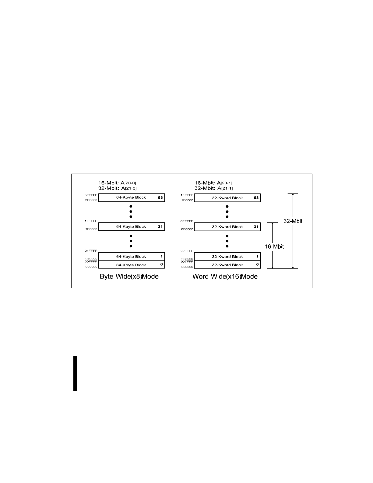
1.2 Product Overview
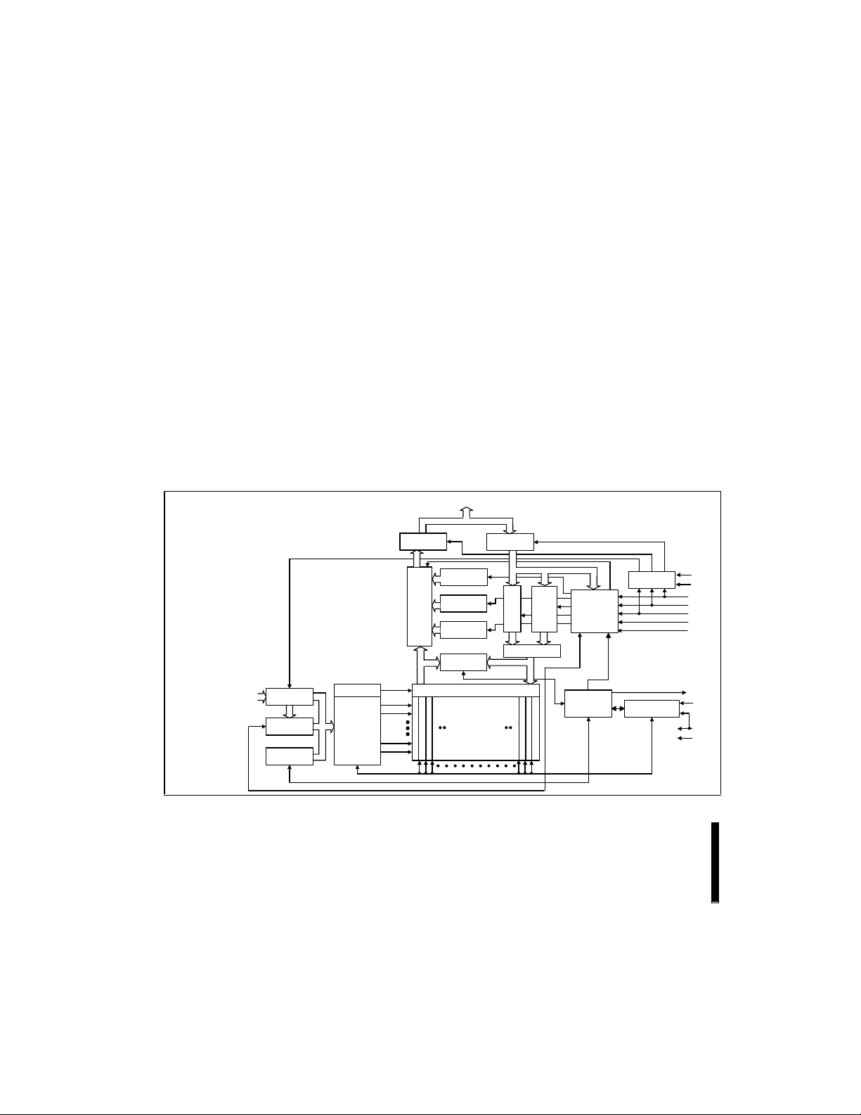
The Word-Wide FlashFile memory family provides
density upgrades with pinout compatibility for the
16- and 32-Mbit densities. They are highperformance memories arranged as 1 Mword and
2 Mwords of 16 bits or 2 Mbyte and 4 Mbyte of
8 bits. This data is grouped in thirty-two and s ixtyfour 64-Kbyte blocks that can be erased, locked
and unlocked in-system. Figure 1 shows the block
diagram, and Figure 5 illustrates the memory
organization.
This family of product s are optimized for fast factory
programming and low power designs. Specifically
designed for 3V systems, the 28F160S3 and
28F320S3 support read operations at 2.7V–3.6V
Vcc with block erase and program operations at
2.7V–3.6V and 5V V
performance is achieved through highly-optimized
write buffers. A 5V V
faster factory programm ing. For a si mple l ow power
design, V
Additionally, the dedic ated V
data protection when V
Internal V
configures the device for optimized write
operations.
A Common Flash Interface (CFI) permits OEMspecified software algori thms to be used for entire
families of devices. This allows device-independent,
JEDEC ID-independent, and forward- and
backward-compatible software support for the
specified flash device families. Flash vendors can
standardize their existing interfaces for long-term
compatibility.
Scaleable Command Set (SCS) allows a single,
simple software driver in all host systems to work
with all SCS-compliant flash memory devices,
independent of system-level packaging (e.g.,
memory card, SIMM, or direc t-to-board placement).
Additionally, SCS provides the highest
system/device data transfer rates and minimizes
device and system-level implementation costs.
A Command User Interface (CUI) serves as the
interface between the system processor and
internal device operation. A valid command
sequence written to the CUI initiates device
automation. An internal Write State M ac hi ne (WSM)
automatically executes the algorithms and timings
necessary for block erase, program, and lock-bit
configuration operations.
A block erase operation erases one of the device’s
64-Kbyte blocks typically within t
independent of other blocks. Each block can be
independently erased 100,000 times. Block erase
suspend mode allows system software to suspend
block erase to read or write data from any other
block.
Data is programmed in byte, word or page
increments. Program suspend mode enables the
system to read data or execute code from any other
flash memory array location.
and VPP can be tied to 2.7V.
CC
detection circuitry automatically
PP
. High programming
PP
option is available for ev en
PP
pin gives complet e
PP
≤ V
PPLK
.
WHQV2/EHQV2
PP
ADVANCE INFORMATION
5
Page 6
28F160S3, 28F320S3 E
The device incorporates two Write Buffers of 32
bytes (16 words) to allow optimum-performance
data programming. This feature can improve
system program performance by up to four times
over non-buffer programming.
Individual block loc king us es a c ombi nation of bl ock
lock-bits to lock and unlock blocks. Block lock-bits
gate block erase, full chi p erase, program and write
to buffer operations. Lock-bit configuration
operations (Set Block Lock-Bit and Clear Block
Lock-Bits commands) set and clear lock-bits.
The Status Register and the STS pin in RY/BY#
mode indicate whether or not the device is busy
executing an operation or ready for a new
command. Polling the Status Register, system
software retrieves WSM f eedback. STS in RY/BY#
mode gives an additional indicator of WSM ac tivity
by providing a hardware status signal. Like the
Status Register, RY/BY#-low indicates that the
WSM is performing a block erase, program , or l ock bit operation. RY/BY#-high indicat es that the WSM
is ready for a new command, block erase is
suspended (and program is inactive), program is
suspended, or the device is in deep power-down
mode.
The Automatic Power Savings (APS) feature
substantially reduces active current when the
device is in static mode (addresses not switching).
The BYTE# pin allows either x 8 or x16 read/writes
to the device. BYTE# at logic low selects 8-bit
mode with address A
byte and high byte. BYTE# at logic high enables
16-bit operation with address A
lowest order address. Addres s A
bit mode.
When one of the CE
pins are at V
CC
selecting between the low
0
becoming the
1
is not used in 16-
0
# pins (CE0#, CE1#) and RP#
X
, the component enters a CMOS
standby mode. Driving RP# t o GND enables a deep
power-down mode which significantly reduces
power consumption, provides write protection,
resets the device, and cl ears the St atus Regis ter. A
reset time (t
) is required from RP# switching
PHQV
high until outputs are valid. Likewise, the device
has a wake time (t
) from RP#-high until writes
PHEL
to the CUI are recognized.
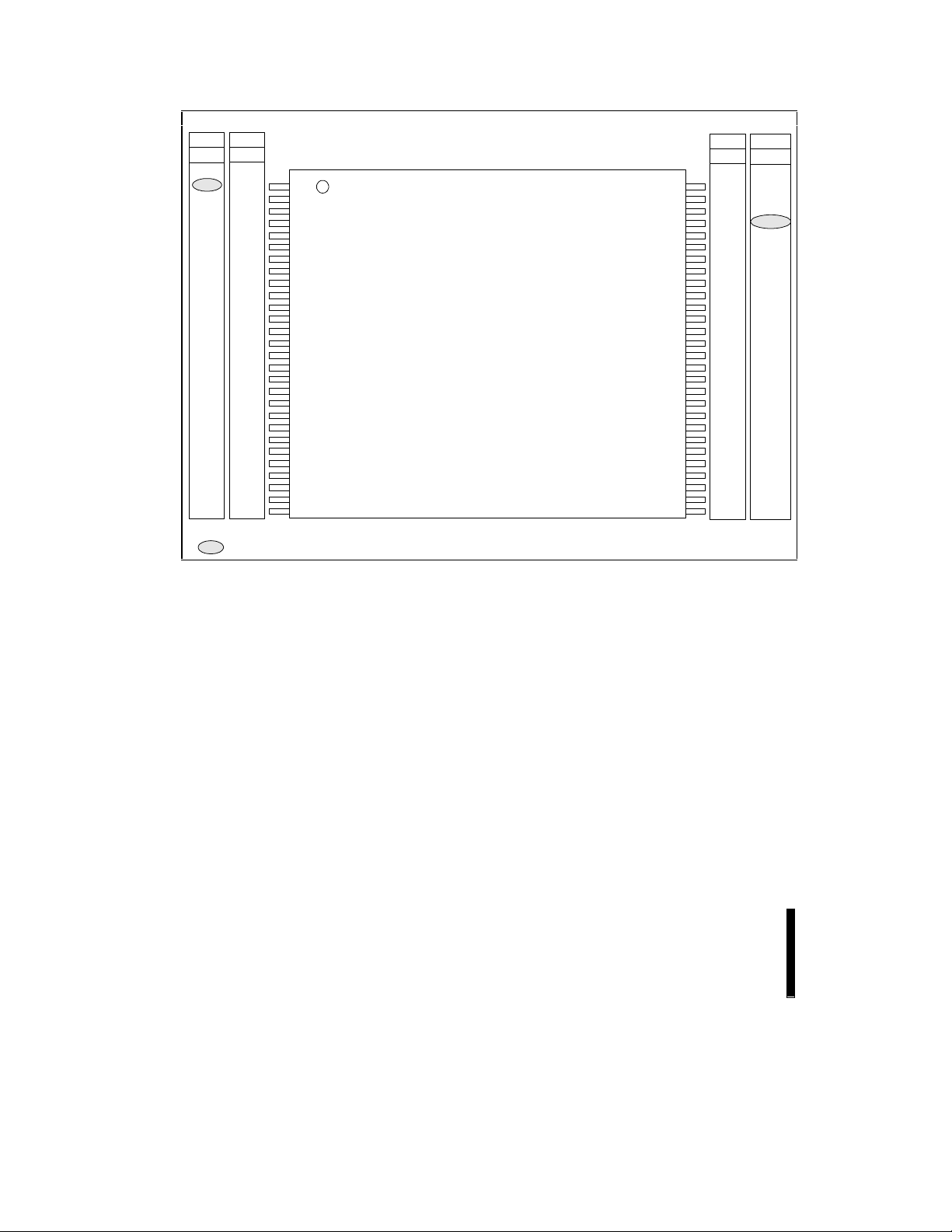
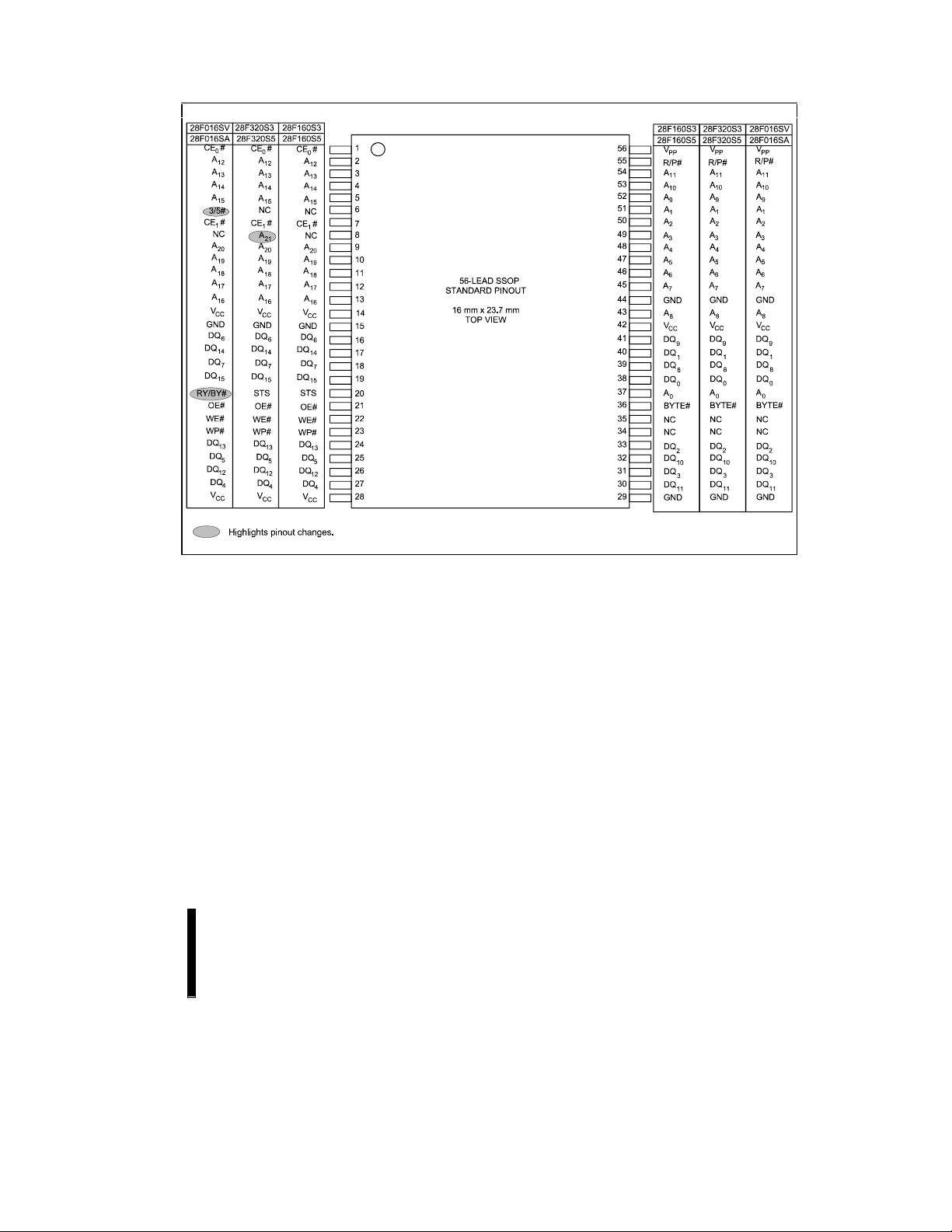
1.3 Pinout and Pin Description
The 16-Mbit device is available in the 56-lead
TSOP, 56-lead SSOP and µBGA packages. The
32- Mb device is available i n the 56-lead S SOP and
µBGA packages. The pinouts are shown in Figures
2, 3 and 4.
DQ0 - DQ
15
16-Mbit: A0- A
32-Mbit: A
0 - A21
20
Input Buffer
Address
Latch
Address
Counter
Y-Decoder
X-Decoder
Output Buffer
Output
Multiplexer
Comparator
16-Mbit: Thirty-two
32-Mbit: Sixty-four
Query
Identifier
Register
Status
Register
Data
Y-Gating
64-Kbyte Blocks
Input Buffer
Data
Register
Multiplexer
V
STS
CC
BYTE#
CE#
WE#
OE#
RP#
WP#
V
PP
V
CC
GND
I/O Logic
Command
User
Interface
Write Buffer
Write State
Machine
Program/Erase
Voltage Switch
Figure 1. Block Diagram
6
ADVANCE INFORMATION
Page 7

E 28F160S3, 28F320S3
Table 1. Pin Descriptions
Sym Type Name and Function
A0–A
DQ
–
DQ
15
CE0#,
CE
#
1
RP# INPUT RESET/DEEP POWER-DOWN: When driven low, RP# inhibits write operations
OE# INPUT OUTPUT ENABLE: Gates the device’s outputs during a read cycle.
WE# INPUT WRITE ENABLE: Controls writes to the CUI and array blocks. Addresses and data
STS OPEN
WP# INPUT WRITE PROTECT: Master control for block locking. When VIL, locked blocks
BYTE# INPUT BYTE ENABLE: Configures x8 mode (low) or x16 mode (high).
V
PP
V
CC
GND SUPPLY GROUND: Do not float any ground pins.
NC NO CONNECT: Lead is not internally connected; it may be driven or floated.
INPUT ADDRESS INPUTS: Address inputs for read and write operations are internally
21
INPUT/
OUTPUT
INPUT CHIP ENABLE: Activates the device’s control logic, input buffers, decoders, and
DRAIN
OUTPUT
SUPPLY BLOCK ERASE, PROGRAM, LOCK-BIT CONFIGURATION POWER SUPPLY:
SUPPLY DEVICE POWER SUPPLY: Do not float any power pins. Do not attempt block
latched during a write cycle. A
In x16 mode, A
DATA INPUTS/OUTPUTS: Inputs data and commands during CUI write cycles;
outputs data during memory array, Status Register, query and identifier code read
cycles. Data pins float to high-impedance when the chip is deselected or outputs
are disabled. Data is internally latched during a write cycle.
sense amplifiers. With CE0# or CE1# high, the device is deselected and power
consumption reduces to standby levels. Both CE
the device. Device selection occurs with the latter falling edge of CE
first rising edge of CE
which provides data protection during system power transitions, puts the device in
deep power-down mode, and resets internal automation. RP#-high enables normal
operation. Exit from deep power-down sets the device to read array mode.
are latched on the rising edge of the WE# pulse.
STATUS: Indicates the status of the internal state machine. When configured in
level mode (default), it acts as a RY/BY# pin. For this and alternate configurations
of the STATUS pin, see the Configuration command. Tie STS to V
resistor.
cannot be erased or programmed, and block lock-bits cannot be set or cleared.
Necessary voltage to perform block erase, program, and lock-bit configuration
operations. Do not float any power pins.
erase, program, or block-lock configuration with invalid V
is not used; input buffer is off.
0
16-Mbit → A
0–A20
# or CE1# disables the device.
0
selects high or low byte when operating in x8 mode.
0
32-Mbit → A0–A
21
# and CE1# must be low to select
0
values.
CC
# or CE1#. The
0
with a pull-up
CC
ADVANCE INFORMATION
7
Page 8
28F160S3, 28F320S3 E
28F016SA
28F016SV
3/5#
3/5#
CE
1
NC
A
20
A
19
A
18
A
17
A
16
V
CC
A
15
A
14
A
13
A
12
CE0#
V
PP
RP#
A
11
A
10
A
9
A
8
GND
A
7
A
6
A
5
A
4
A
3
A
2
A
1
#
28F160S3
28F160S5
NC
CE
1
NC
A
20
A
19
A
18
A
17
A
16
V
CC
A
15
A
14
A
13
A
12
CE0#
V
PP
RP#
A
11
A
10
A
9
A
8
GND
A
7
A
6
A
5
A
4
A
3
A
2
A
1
1 56
#
2 55
3 54
4 53
5 52
6 51
7 50
8 49
9 48
10 47
11 46
12 45
13 44
14 43
15 42
16 41
17 40
18 39
19 38
20 37
21 36
22 35
23 34
24 33
25 32
26 31
27 30
28 29
56-LEAD TSOP
STANDARD PINOUT
14 mm x 20 mm
TOP VIEW
28F160S3
28F160S5
WP#
WE#
OE#
STS
DQ
15
DQ
DQ
14
DQ
GND
DQ
13
DQ
DQ
12
DQ
V
CC
GND
DQ
11
DQ
DQ
10
DQ
V
CC
DQ
DQ
DQ
DQ
A
0
BYTE#
NC
NC
7
6
5
4
3
2
9
1
8
0
28F016SA
28F016SV
WP#
WE#
OE#
RY/BY#
RY/BY#
DQ
15
DQ
7
DQ
14
DQ
6
GND
DQ
13
DQ
5
DQ
12
DQ
4
V
CC
GND
DQ
11
DQ
3
DQ
10
DQ
2
V
CC
DQ
9
DQ
1
DQ
8
DQ
0
A
0
BYTE#
NC
NC
Highlights pinout changes.
Figure 2. TSOP 56-Lead Pinout
8
ADVANCE INFORMATION
Page 9
E 28F160S3, 28F320S3
Figure 3. SSOP 56-Lead Pinout
ADVANCE INFORMATION
9
Page 10
28F160S3, 28F320S3 E
GND A10 VPP CE0 A14 VCC
A4 A7 A9 A11 A12 A15 A17 A19
A5 A6 A8 RP# A13 A16 A21 A20
A2 A1 A3 A18 CE1 NC
NC NC BYTE# DQ7 WP# WE#
A0 DQ8 DQ1 DQ3 DQ12DQ6 DQ15OE#
DQ0 DQ9 DQ2 DQ11DQ4 DQ13DQ14 STS
VCC DQ10 GND VCC DQ5 GND
Bottom View
NOTES:
1. Figures are not drawn to scale.
2. Address A21 is not included in the 28F160S3.
3. More information on µBGA* packages is available by contacting your Intel/Distribution sales office.
This is the view of the package as surface mounted on
the board. Note that the signal s are mirror imaged.
GNDA10VPPCE0A14VCC
NCNCBYTE#DQ7WP#WE#
DQ0DQ9DQ2DQ11DQ4DQ13DQ14 STS
VCCDQ10 GNDVCCDQ5GND
Figure 4. µBGA* Package Pinout
A4A7A9A11A12A15A17A19
A5A6A8RP#A13A16A21A20
A2A1A3A18CE1NC
A0DQ8DQ1DQ3DQ12DQ6DQ15OE#
2.0 PRINCIPLES OF OPERATION
The word-wide memories include an on-chip
Write State Machine (WSM) to manage block
erase, program, and lock-bit configuration
functions. It allows for: 100% TTL-level control
inputs, fixed power suppli es duri ng block erasure,
programming, lock-bit c onfiguration, and minimal
processor overhead with RAM-like interface
timings.
After initial device power-up or return from deep
power-down mode (see Bus Operations), the
10
device defaults to read array mode. Manipul ation
of external memory control pins all ow array read,
standby, and output disable operations.
Read Array, Status Regis ter, query , and identif ier
codes can be accessed through the CUI
independent of the V
programming voltage on V
voltage. Proper
PP
enables successful
PP
block erasure, program, and lock-bit
configuration. All functions associated with
altering memory contents—bloc k erase, program,
lock-bit configuration—are acces sed via the CUI
and verified through the Status Register.
ADVANCE INFORMATION
Page 11
E 28F160S3, 28F320S3
Commands are written using standard microprocessor write timings. The CUI c ontents serve
as input to the WSM that controls the block
erase, programming, and lock-bit configuration.
The internal algorithms are regulated by the
WSM, including pulse repetition, internal
verification, and margining of data. Addresses
and data are internally latched during write
cycles. Writing the appropriate command outputs
array data, identifier codes, or Status Register
data.
Interface software that initiates and polls
progress of block erase, program ming, and lockbit configuration can be stored in any bl ock. This
code is copied to and executed from system
RAM during flash memory updates. After
successful com pletion, reads are again possible
via the Read Array command. Block erase
suspend allows system software to suspend a
block erase to read or write dat a from any other
block. Program suspend all ows system software
to suspend a program to read data from any
other flash memory array location.
2.1 Data Protection
Depending on the application, the system
designer may choose to make the V
supply switchable or hardwired to V
device supports either design practice, and
encourages optimization of the processormemory interface.
When V
altered. When high voltage is appli ed to V
two-step block erase, program, or lock-bit
configuration command sequences provide
protection from unwanted operations. All write
functions are disabled when V
the write lockout v oltage V
V
IL
provides additional protection from inadvertent
code or data alteration.
≤ V
PP
. The device’s block locking capability
, memory contents cannot be
PPLK
voltage is below
CC
or when RP# is at
LKO
PP
PPH1/2
power
. The
, the
PP
ADVANCE INFORMATION
Figure 5. Memory Map
11
Page 12

28F160S3, 28F320S3 E
3.0 BUS OPERATION
The local CPU reads and writes fl ash m emory i nsystem. All bus cycles to or from the flash
memory conform to standard mic roprocessor bus
cycles.
3.1 Read
Block information, query information, identifier
codes and Status Registers can be read
independent of the V
voltage.
PP
The first task is to place the device into the
desired read mode by writing the appropriate
read-mode command (Read Array, Query, Read
Identifier Codes, or Read Stat us Register) to t he
CUI. Upon initial device power-up or after exit
from deep power-down mode, the device
automatically reset s to read array mode. Control
pins dictate the data flow in and out of the
component. CE
active to obtain data at the outputs. CE
CE
# are the device selection controls, and,
1
#, CE1# and OE# must be driven
0
# and
0
when both are active, enable the selected
memory device. OE# is the data output (DQ
DQ
) control: When active it drives the selected
15
0
memory data onto the I/O bus. WE# must be at
V
and RP# must be at VIH. Figure 17 illustrates
IH
a read cycle.
3.2 Output Disable
With OE# at a logic-high level (VIH), the device
outputs are disabled. Output pins DQ
–DQ15 are
0
placed in a high-impedance state.
3.3 Standby
CE0# or CE1# at a logic-high level (VIH) places
the device in standby mode, substantially
reducing device power consumption. DQ
(or DQ0– DQ7 in x8 mode) outputs are placed in
a high-impedance state independent of OE#. If
deselected during block erase, programming, or
lock-bit configuration, the device continues
functioning and consuming act ive power until the
operation completes.
–DQ
0
3.4 Deep Power-Down
RP# at VIL initiates the deep power-down mode.
In read mode, RP#-low deselects the memory,
places output drivers in a high-impedance state,
and turns off all internal circuits. RP# must be
held low for time t
PLPH
. Time t
is required
PHQV
after return from power-down until initial memory
access outputs are valid. After this wake-up
interval, normal operation is restored. The CUI
resets to read array mode, and the Status
Register is set to 80H.
During block erase, programming, or lock-bit
configuration modes, RP#-low will abort the
operation. STS in RY/BY# mode remains low
until the reset operation is complete. Memory
contents being altered are no longer valid; the
data may be partially corrupted after
programming or partially altered af ter an erase or
lock-bit configuration. Time t
RP# goes to logic-high (V
command can be written.
is required after
PHWL
) before another
IH
It is important in any automated system to assert
–
RP# during system reset. When the system
comes out of reset, it expects to read from the
flash memory. Automated flash memories
provide status informat ion when access ed during
block erase, programming, or lock-bit
configuration modes. I f a CPU reset occurs with
no flash memory reset , proper CPU initialization
may not occur because the f las h memory may be
providing status inform ati on inst ead of array data.
Intel’s Flash memories allow proper CPU
initialization following a system reset through the
use of the RP# input. In t his application, RP# is
controlled by the same RESET# signal that
resets the system CPU.
3.5 Read Query Operation
15
The read query operation outputs block status,
Common Flash Interface (CFI) ID string, system
interface, device geometry, and Intel-specific
extended query information.
12
ADVANCE INFORMATION
Page 13

E 28F160S3, 28F320S3
3.6 Read Identifier Codes
Operation
The read-identifier codes operation outputs the
manufacturer code, devic e code, and block lock
configuration codes for each block configuration
(see Figure 6). Using the manufacturer and
device codes, the system software can
automatically match the device with its proper
algorithms. The block-lock configuration codes
identify each block’s lock-bit setting.
3.7 Write
Writing commands to the CUI enables reading of
device data, query, identifier codes, inspection
and clearing of the Status Register. Additionally,
when V
and lock-bit configuration can also be performed.
The Block Erase command requires appropriate
command data and an address within the block
to be erased. The Byte/Word Write command
requires the command and address of the
location to be written. Set Block Lock-Bit
commands require the command and address
within the block to be locked. The Clear Block
Lock-Bits command requires the command and
an address within the device.
The CUI does not occupy an addressable
memory location. I t is written when WE#, CE
and CE
and data needed to execute a command are
latched on the rising edge of WE# or CE
(CE
Standard microprocessor writ e timings are used.
Figure 18 illustrates a write operation.
= V
PP
# are active and OE# = VIH. The address
1
#, CE1#), whichever goes high first.
0
, block erasure, programming,
PPH1/2
0
X
4.0 COMMAND DEFINITIONS
VPP voltage ≤ V
from the Status Register, identifier codes, or
memory blocks. Placing V
successful bloc k erase, programming, and lockbit configuration operations.
enables read operations
PPLK
on VPP enables
PPH1/2
#,
#
Figure 6. Device Identifier Code Memory Map
ADVANCE INFORMATION
Device operations are selec ted by writ ing spec ifi c
commands into the CUI. and Table 3 define
these commands.
13
Page 14
28F160S3, 28F320S3 E
Table 2. Bus Operations
Mode Notes RP# CE0#CE1# OE#
Read 1,2 V
Output Disable V
Standby V
Reset/Power-
10 V
Down Mode
Read Identifier
4VIHV
Codes
Read Query 5 V
Write 3,6,7 V
V
IH
IL
V
IH
IL
V
IH
IL
V
IH
V
IH
X X X X X X High Z High Z
IL
IL
V
IH
IL
V
IH
IL
V
IL
V
IL
V
IH
V
IL
V
IH
V
IL
V
IL
V
IL
(11)
V
IL
V
IH
X X X X High Z X
V
IL
V
IL
V
IH
NOTES:
1. Refer to Table 19. When V
2. X can be V
or VIH for control and address input pins and V
IL
≤ V
PP
, memory contents can be read, but not altered.
PPLK
PPLK
voltages.
3. STS in level RY/BY# mode (default) is V
configuration algorithms. It is V
OH
when the WSM is executing internal block erase, programming, or lock-bit
OL
when the WSM is not busy, in block erase suspend mode (with programming inactive),
program suspend mode, or deep power-down mode.
4. See Section 4.3 for read identifier code data.
5. See Section 4.2 for read query data.
6. Command writes involving block erase, write, or lock-bit configuration are reliably executed when V
V
= V
CC
7. Refer to Table 3 for valid D
8. DQ refers to DQ
9. High Z will be V
(see Section 6.2).
CC1/2
if BYTE# is low and DQ
0–7
with an external pull-up resistor.
OH
during a write operation.
IN
if BYTE# is high.
0–15
10. RP# at GND ± 0.2V ensures the lowest deep power-down current.
11. OE# = V
and WE# = VIL concurrently is an undefined state and should not be attempted.
IL
(11)
WE#
V
IH
V
IH
V
IH
Address V
PP
XXD
X X High Z X
See
XD
Figure 6
VIHSee Table 6 X D
or V
V
PPH1/2
IL
XV
PPH1/2
for VPP. See Table 19, for V
(8)
DQ
OUT
OUT
OUT
D
IN
and V
PPLK
= V
PP
PPH1/2
and
STS
High Z
High Z
PPH1/2
(3)
X
X
(9)
(9)
(9)
14
ADVANCE INFORMATION
Page 15

E 28F160S3, 28F320S3
Table 3. Word-Wide FlashFile™ Memory Command Set Definitions
Command Scaleable
Read Array SCS/BCS 1 Write X FFH
Read Identifier Codes SCS/BCS ≥2 5 Write X 90H Read IA ID
Read Query SCS ≥ 2 Write X 98H Read QA QD
Read Status Register SCS/BCS 2 Write X 70H Read X SRD
Clear Status Register SCS/BCS 1 Write X 50H
Write to Buffer SCS > 2 8, 9, 10 Write BA E8H Write BA N
Word/Byte Program SCS/BCS 2 6,7 Write X 40H
Block Erase SCS/BCS 2 6,10 Write X 20H Write BA D0H
Block Erase, Word/Byte
Program Suspend
Block Erase, Word/Byte
Program Resume
STS pin Configuration SCS 2 Write X B8H Write X CC
Set Block Lock-Bit SCS 2 11 Write X 60H Write BA 01H
Clear Block Lock-Bits SCS 2 12 Write X 60H Write X D0H
Full Chip Erase SCS 2 10 Write X 30H Write X D0H
or Basic
Command
Set
SCS/BCS 1 6 Write X B0H
SCS/BCS 1 6 Write X D0H
(14)
Bus
Cycles
Req'd
Notes First Bus Cycle Second Bus Cycle
Oper
(1)
Addr
(2)
Data
10H
(3,4)
or
(13)
(1)
Oper
Write PA PD
Addr
(2)
Data
(3,4)
ADVANCE INFORMATION
15
Page 16

28F160S3, 28F320S3 E
NOTES:
1. Bus operations are defined in Table 2.
2. X = Any valid address within the device.
BA = Address within the block being erased or locked.
IA = Identifier Code Address: see Table 12.
QA = Query database Address.
PA = Address of memory location to be programmed.
3. ID = Data read from Query database.
SRD = Data read from Status Register. See Table 15 for a description of the Status Register bits.
PD = Data to be programmed at location PA. Data is latched on the rising edge of WE#.
CC = Configuration Code. (See Table 14.)
4. The upper byte of the data bus (DQ
5. Following the Read Identifier Codes command, read operations access manufacturer, device, and block-lock codes. See
Section 4.3 for read identifier code data.
6. If a block is locked (i.e., the block’s lock-bit is set to 0), WP# must be at V
suspend operations. Attempts to issue a block erase, program and suspend operation to a locked block while WP# is V
will fail.
7. Either 40H or 10H are recognized by the WSM as the byte/word program setup.
8. After the Write to Buffer command is issued, check the XSR to make sure a Write Buffer is available.
9. N = byte/word count argument such that the number of bytes/words to be written to the input buffer = N + 1. N = 0 is 1
byte/word length, and so on. Write to Buffer is a multi-cycle operation, where a byte/word count of N + 1 is written to the
correct memory address (WA) with the proper data (WD). The Confirm command (D0h) is expected after exactly N + 1 write
cycles; any other command at that point in the sequence aborts the buffered write. Writing a byte/word count outside the
buffer boundary causes unexpected results and should be avoided.
10. The write to buffer, block erase, or full chip erase operation does not begin until a Confirm command (D0h) is issued.
Confirm also reactivates suspended operations.
11. A block lock-bit can be set only while WP# is V
12. WP# must be at V
to clear block lock-bits. The clear block lock-bits operation simultaneously clears all block lock-bits.
IH
13. Commands other than those shown above are reserved for future use and should not be used.
14. The Basic Command Set (BCS) is the same as the 28F008SA Command Set or Intel Standard Command Set. The
Scaleable Command Set (SCS) is also referred to as the Intel Extended Command Set.
) during command writes is a “Don’t Care” in x16 operation.
8–15
in order to perform block erase, program and
IH
.
IH
IL
16
ADVANCE INFORMATION
Page 17

E 28F160S3, 28F320S3
4.1 Read Array Command
Upon initial device power-up and after exit from
deep power-down mode, the device defaul ts to read
array mode. This operation is also initiated by
writing the Read Array command. The device
remains enabled for reads until another command
is written. Once the int ernal WS M has st arted bloc k
erase, program, or lock-bit confi guration, the device
will not recognize the Read Array command until
the WSM completes it s operation—unless the WSM
is suspended via an Erase-Suspend or ProgramSuspend command. The Read Array command
functions independently of the V
voltage.
PP
4.2 Read Query Mode Command
This section defines the data structure or
“database” returned by the Common Fl ash Interface
(CFI) Query command. System software should
parse this structure t o gain critic al informati on such
as block size, density, x8/x16, and electrical
specifications. Once this information has been
obtained, the software will know which command
sets to use to enable fl ash writes, bloc k erases, and
otherwise control the flas h component. The Query
is part of an overall specification for multiple
command set and control interface descriptions
called Common Flash Interface, or CFI.
4.2.1 QUERY STRUCTURE OUTPUT
The Query “database” allows system software to
gain critical information for controlling the flash
component. This section describes the device’s
CFI-compliant interface that allows the host system
to access Query data.
Query data are always presented on the lowestorder data outputs (DQ
offset value is the address rel ative to the max imum
bus width supported by the device. On t his device,
the Query table device starting address is a 10h
word address, since the maximum bus width is x16.
For this word-wide (x16) device, t he first two bytes
of the Query structure, “Q” and ”R” in ASCII, appear
on the low byte at word addresses 10h and 11h.
This CFI-compliant device outputs 00H data on
upper bytes. Thus, the dev ice outputs ASCII “Q” in
the low byte (DQ
(DQ
).
8-15
Since the device is x 8/x16 capable, the x8 data is
still presented in word-relative (16-bit) addresses.
However, the “fill data” (00h) is not the same as
driven by the upper bytes in the x16 mode. As in
x16 mode, the byte address (A
Query output so that the “odd byte address” (A
high) repeats the “even byte address” dat a (A0 low).
Therefore, in x8 mode using byte addressing, the
device will output the sequence “Q”, “Q”, “R”, “R”,
“Y”, “Y”, and so on, beginning at byte-relative
address 20h (which is equivalent to word offs et 10h
in x16 mode).
At Query addresses containing two or more bytes
of information, the least significant data byte is
presented at the lower address, and the most
significant data byte is presented at the higher
address.
0-7
) only. The numerical
0-7
) and 00h in the high byte
) is ignored for
0
0
ADVANCE INFORMATION
17
Page 18

28F160S3, 28F320S3 E
Address
Byte Addressing:
Table 4. Summary of Query Structure Output as a Function of Device and Mode
Device Type/Mode Word Addressing Byte Addressing
Location Query Data
Hex, ASCII
x16 device/
x16 mode
x16 device/
10h
11h
12h
N/A
(1)
0051h “Q”
0052h “R”
0059h “Y”
N/A 20h
x8 mode
NOTE:
1. The system must drive the lowest order addresses to access all the device’s array data when the device is configured in x8
mode. Therefore, word addressing where lower addresses are not toggled by the system is “Not Applicable” for x8configured devices.
Table 5. Example of Query Structure Output of a x16- and x8-Capable Device
Device
Address
A16–A
0010h
0011h
0012h
0013h
0014h
0015h
0016h
0017h
0018h
...
1
Word Addressing:
0051h “Q”
0052h “R”
0059h “Y”
P_ID
P_ID
P
P
A_ID
A_ID
LO
HI
LO
HI
LO
HI
PrVendor
ID #
PrVendor
TblAdr
AltVendor
ID #
...
Query Data
D15–D
0
Location Query Data
20h
21h
22h
21h
22h
Byte
A7–A
0
20h
21h
22h
23h
24h
25h
26h
27h
28h
...
51h “Q”
51h “Q”
52h “R”
52h “R”
59h “Y”
59h “Y
P_IDLO PrVendor
P_ID
ID #
LO
P_ID
HI
...
Hex, ASCII
51h “Q”
00h null
52h “R”
51h “Q”
51h “Q”
52h “R”
Query Data
D7–D
0
”
“
18
ADVANCE INFORMATION
Page 19

E 28F160S3, 28F320S3
4.2.2 QUERY STRUCTURE OVERVIEW
The Query command causes the flas h component
to display the Common Flas h Interface (CFI ) Query
structure or “database.” The struc ture sub-sections
and address locations are summarized in Table 8.
The following sections des cribe the Query s tructure
sub-sections in detail.
Table 6. Query Structure
Offset Sub-Section Name Description
00h Manufacturer Code
01h Device Code
(3)
32 Kword).
(2)
Block Status Register Block-specific information
Reserved Reserved for vendor-specific information
Primary Intel-Specific Extended Query
Table
(BA+2)h
04-0Fh
10h CFI Query Identification String Command set ID and vendor data offset
1Bh System Interface Information Device timing & voltage information
27h Device Geometry Definition Flash device layout
P
NOTES:
1. Refer to Section 4.2.1 and Table 4 for the detailed definition of offset address as a function of device word width and mode.
2. BA = The beginning location of a Block Address (i.e., 08000h is the beginning location of block 1 when the block size is
3. Offset 15 defines “P” which points to the Primary Intel-specific Extended Query Table.
(1)
Vendor-defined additional information
specific to the Primary Vendor Algorithm
ADVANCE INFORMATION
19
Page 20

28F160S3, 28F320S3 E
/
4.2.3 BLOCK STATUS REGISTER
Block Erase Status (BSR.1) allows system software
to determine the success of the last block erase
The Block Status Register indicates whether an
erase operation completed succes sfully or whether
a given block is lock ed or can be ac ces sed f or flas h
program/erase operations.
operation. BSR.1 can be used just after power-up to
verify that the V
supply was not accidentally
CC
removed during an erase operation. This bit is onl y
reset by issuing another erase operation to the
block. The Block Status Register is accessed from
word address 02h within each block.
Table 7. Block Status Register
Offset Length
(bytes)
Description 28F320S3
28F160S3
x16 Device/Mode
(1)
(BA+2)h
01h Block Status Register BA+2: 0000h or
0001h
BSR.0 = Block Lock Status
BA+2 (bit 0): 0 or 1
1 = Locked
0 = Unlocked
BSR.1 = Block Erase Status
BA+2 (bit 1): 0 or 1
1 = Last erase operation did not complete
successfully
0 = Last erase operation completed successfully
BSR 2-7 Reserved for future use
NOTE:
1. BA = The beginning location of a Block Address (i.e., 008000h is the beginning location of block 1 in word mode.)
BA+2 (bits 2-7): 0
20
ADVANCE INFORMATION
Page 21

E 28F160S3, 28F320S3
/
4.2.4 CFI QUERY IDENTIFICATION STRING
The Identification String provides verification that
the component supports the Common Flash
Interface specification. Additionally, it indicates
which version of the specification and which
vendor-specified command set(s) is (are)
supported.
Table 8. CFI Identification
Offset Length
10h 03h Query-Unique ASCII string “QRY“ 10: 0051h
13h 02h Primary Vendor Command Set and Control Interface ID Code
15h 02h Address for Primary Algorithm Extended Query Table
17h 02h Alternate Vendor Command Set and Control Interface ID Code
19h 02h Address for Secondary Algorithm Extended Query Table
(Bytes)
16-bit ID Code for Vendor-Specified Algorithms
Offset value =
Second Vendor-Specified Algorithm Supported
Note: 0000h means none exists
Note: 0000h means none exists
P
Description 28F320S3
= 31h
28F160S3
11: 0052h
12: 0059h
13: 0001h
14: 0000h
15: 0031h
16: 0000h
17: 0000h
18: 0000h
19: 0000h
1A: 0000h
ADVANCE INFORMATION
21
Page 22

28F160S3, 28F320S3 E
/
4.2.5 SYSTEM INTERFACE INFORMATION
The following device information can be useful in
optimizing system interface software.
Table 9. System Interface Information
Offset Length
(bytes)
1Bh 01h VCC Logic Supply Minimum Program/Erase Voltage
bits 7–4 BCD volts
bits 3–0 BCD 100 mv
1Ch 01h VCC Logic Supply Maximum Program/Erase Voltage
bits 7–4 BCD volts
bits 3–0 BCD 100 mv
1Dh 01h VPP [Programming] Supply Minimum Program/Erase Voltage
bits 7–4 HEX volts
bits 3–0 BCD 100 mv
1Eh 01h VPP [Programming] Supply Maximum Program/Erase Voltage
bits 7–4 HEX volts
bits 3–0 BCD 100 mv
1Fh 01h Typical Time-Out per Single Byte/Word Program, 2N µ-sec 1F: 0003h
20h 01h Typical Time-Out for Max. Buffer Write, 2N µ-sec 20: 0006h
21h 01h Typical Time-Out per Individual Block Erase, 2N m-sec 21: 000Ah
22h 01h Typical Time-Out for Full Chip Erase, 2N m-sec 22: 000Fh
23h 01h Maximum Time-Out for Byte/Word Program,
N
2
Times Typical
24h 01h Maximum Time-Out for Buffer Write, 2N Times Typical 24: TBD
25h 01h Maximum Time-Out per Individual Block Erase,
N
2
Times Typical
26h 01h Maximum Time-Out for Chip Erase, 2
Description 28F320S3
28F160S3
1B: 0030h
1C: 0055h
1D: 0030h
1E: 0055h
23: TBD
25: TBD
N
Times Typical 26: TBD
22
ADVANCE INFORMATION
Page 23

E 28F160S3, 28F320S3
/
4.2.6 DEVICE GEOMETRY DEFINITION
This field provides cri tical det ails of the f lash device
geometry.
Table 10. Device Geometry Definition
Offset Length
(bytes)
27h 01h Device Size = 2N in Number of Bytes 27: 0015h
28h 02h Flash Device Interface Description
value
0002h x8/x16 asynchronous
2Ah 02h Maximum Number of Bytes in Write Buffer = 2
2Ch 01h Number of Erase Block Regions within Device:
bits 7–0 = x = # of Erase Block Regions
2Dh 04h Erase Block Region Information
bits 15–0 = y, Where y+1 = Number of Erase Blocks of
Identical Size within Region
bits 31–16 = z, Where the Erase Block(s) within This Region
are (z) × 256 Bytes
Description 28F320S3
meaning
N
28F160S3
(16Mb)
27: 0016h
(32Mb)
28: 0002h
29: 0000h
2A: 0005h
2B: 0000h
2C: 0001h
y: 32 Blk
(16Mb)
2D: 001Fh
2E: 0000h
y: 64 Blk
(32Mb)
2D: 003Fh
2E: 0000h
z: 64-KB
2F: 0000h
30: 0001h
ADVANCE INFORMATION
23
Page 24

28F160S3, 28F320S3 E
4.2.7 INTEL-SPECIFIC EXTENDED QUERY
Certain flash features and c ommands are optional.
The Intel-Specific Extended Query table specifies
this and other similar types of information.
Offset
(P)h 03h Primary Extended Query Table
(P+3)h 01h Major Version Number, ASCII 34: 0031h
(P+4)h 01h Minor Version Number, ASCII 35: 0030h
(P+5)h 04h Optional Feature & Command Support
TABLE
(1)
Length
(bytes)
Table 11. Primary-Vendor Specific Extended Query
Description
Unique ASCII String “PRI“
bit 0 Chip Erase Supported (1=yes, 0=no)
bit 1 Suspend Erase Supported (1=yes, 0=no)
bit 2 Suspend Program Supported (1=yes, 0=no)
bit 3 Lock/Unlock Supported (1=yes, 0=no)
bit 4 Queued Erase Supported (1=yes, 0=no)
Data
31: 0050h
32: 0052h
33: 0049h
36: 000Fh
37: 0000h
38: 0000h
39: 0000h
bits 5–31 Reserved for future use; undefined bits
are “0”
(P+9)h 01h Supported Functions after Suspend
Read Array, Status, and Query are always supported during
suspended Erase or Program operation. This field defines
other operations supported.
bit 0 Program Supported after Erase Suspend
(1=yes, 0=no)
3A: 0001h
bits 1-7 Reserved for future use; undefined bits are “0”
(P+A)h 02h Block Status Register Mask
Defines which bits in the Block Status Register section of
Query are implemented.
bit 0 Block Status Register Lock-Bit [BSR.0] active
(1=yes, 0=no)
bit 1 Block Erase Status Bit [BSR.1] active
(1=yes, 0=no)
3B: 0003h
3C: 0000h
bits 2-15 Reserved for future use; undefined bits
are “0”
NOTES:
1. The variable P is a pointer which is defined at offset 15h in Table 8.
24
ADVANCE INFORMATION
Page 25

E 28F160S3, 28F320S3
Table 11. Primary-Vendor Specific Extended Query (Continued)
Offset Length
(P+C)h 01h VCC Logic Supply Optimum Program/Erase voltage (highest
(P+D)h 01h VPP [Programming] Supply Optimum Program/Erase voltage
(P+E)h
(bytes)
performance)
bits 7–4 BCD value in volts
bits 3–0 BCD value in 100 mv
bits 7–4 HEX value in volts
bits 3–0 BCD value in 100 mv
reserved Reserved for future use
Description
Data
3D: 0050h
3E: 0050h
Table 12. Identifier Codes
(1)
(1)
(2)
Data
2-7
DQ1 = 0
DQ1 = 1
2-7
Code Address
Manufacturer Code 000000 B0
Device Code 16 Mbit 000001 D0
32 Mbit 000001 D4
Block Lock Configuration X0002
• Block is Unlocked DQ0 = 0
• Block is Locked DQ0 = 1
• Reserved for Future Use DQ
Block Erase Status x0002
• Last erase completed
successfully
• Last erase did not
complete successfully
• Reserved for Future Use DQ
NOTES:
1. X selects the specific block lock configuration code.
See Figure 6 for the device identifier code memory
map.
2. A
should be ignored in this address. The lowest order
0
address line is A
in both word and byte mode.
1
4.3 Read Identifier Codes
Command
The identifier code operation is initiat ed by writing
the Read Identifier Codes c ommand. Following the
command write, read cycles from addresses shown
in Figure 6 retrieve the manufacturer, device, block
lock configuration, and block erase status codes
(see Table 12 for identifier code values). To
terminate the operation, write another valid
command. Like the Read Array command, the
Read Identifier Codes command functions
independently of the V
Read Identifier Codes command, the information in
Table 12 can be read.
voltage. Following the
PP
4.4 Read Status Register
Command
The Status Register may be read to determine
when programming, block erasure, or lock-bit
configuration is compl ete and whet her the operati on
completed success fully. It may be read at any time
by writing the Read Status Register command.
After writing this command, all subsequent read
operations output data from the Status Register
until another valid command i s written. The Status
Register contents are latched on the falling edge of
OE#, CE
CE
Register latch. The Read Status Register c ommand
functions independently of the V
#, or CE1# whichever occurs last. OE# or
0
# must toggle to VIH to update the Status
X
voltage.
PP
ADVANCE INFORMATION
25
Page 26

28F160S3, 28F320S3 E
Following a program, block erase, set block loc k-bit,
or clear block lock-bits command sequence, only
SR.7 is valid until the Write State Machine
completes or suspends the operation. Device I/O
pins DQ
and DQ
0-6
are invalid. When the
8-15
operation completes or suspends (SR.7 = 1), all
contents of the Status Register are valid when read.
The eXtended Status Register (XSR) may be read
to determine Write Buffer availability (see Table 16).
The XSR may be read at any time by writing the
Write to Buffer command. After writing this
command, all subsequent read operations output
data from the XSR, until another v alid command is
written. The contents of the XSR are latc hed on t he
falling edge of OE# or CE
# whichever occurs last
X
in the read cycle. Write to buffer command must be
re-issued to update the XSR latch.
4.5 Clear Status Register
Command
Status Register bits SR.5, SR.4, SR.3, and SR.1
are set to “1”s by the WSM and can only be reset
by the Clear Status Regis ter command. These bits
indicate various failure conditions (see Table 15).
By allowing system software to reset these bits,
several operations (such as cumulativ ely erasing or
locking multiple blocks or programming several
bytes/words in sequence) m ay be performed. The
Status Register may be polled to determine if an
error occurred during the sequence.
To clear the Status Register, the Clear Status
Register command is written. It functions
independently of the applied V
command is not functional during block erase or
voltage. This
PP
program suspend modes.
4.6 Block Erase Command
Block Erase is executed one block at a time and
initiated by a two-cycle command. A Block Erase
Setup command is written first, followed by a
Confirm command. This command sequence
requires appropriate sequencing and an address
within the block to be erased (erase changes all
block data to FFH). Block preconditioning, erase,
and verify are handled internally by the WSM
(invisible to the system). After the two-cycle block
erase sequence is written, the devi ce automatically
outputs Status Regis ter dat a when read (s ee Figure
10). The CPU can detect block erase c omplet ion by
analyzing STS in level RY/BY# mode or Status
Register bit SR.7. Toggle OE#, CE
#, or CE1# to
0
update the Status Register.
When the block erase is complete, St atus Register
bit SR.5 should be check ed. If a block erase error is
detected, the Status Register should be cleared
before system software attempts corrective actions.
The CUI remains in read Status Regi st er mode unti l
a new command is issued.
This two-step command sequence of set-up
followed by execution ensures t hat block contents
are not accidentally erased. An invalid Block Erase
command sequence will result in both Status
Register bits SR.4 and SR.5 being set to “1.” A lso,
reliable block erasure can only occur when
V
CC
= V
and VPP = V
CC1/2
. In the absence of
PPH1/2
these voltages, block contents are protected
against erasure. If block erase is attempted while
V
≤ V
PP
Successful block erase requires that the
, SR.3 and SR.5 will be set to “1.”
PPLK
corresponding block lock-bit be cleared, or WP# =
V
. If block erase is attempted when the
IH
corresponding block lock-bit is set and WP# = V
the block erase will fail and SR.1 and SR.5 will be
set to “1.”
4.7 Full Chip Erase Command
The Full Chip Erase command followed by a
Confirm command erases all unl ocked blo cks. After
the Confirm command is writ ten, the device erases
all unlocked blocks from block 0 to block 31 (or 63)
sequentially. Block preconditioning, erase, and
verify are handled internally by t he WSM. After the
Full Chip Erase command sequence is written to
the CUI, the device autom atically outputs the Status
Register data when read. The CPU can detect full
chip erase completion by polling the STS pin in
level RY/BY# mode or Status Register bit SR.7.
When the full chip erase is complete, Status
Register bit SR.5 should be c hecked to see if the
operation completed successf ully. If an erase error
occurred, the Status Register should be cleared
before issuing the next command. The CUI rem ains
in read Status Register mode until a new command
is issued. If an error is detected while erasing a
block during a full chip eras e operation, the WSM
skips the remaining cel ls i n that block and proceeds
to erase the next block. Reading the block valid
status code by issuing the Read Identifier Codes
command or Query command informs the user of
which block(s) failed to erase.
IL,
26
ADVANCE INFORMATION
Page 27

E 28F160S3, 28F320S3
This two-step command sequence of setup followed
by execution ensures that block contents are not
accidentally erased. An invalid Full Chip Erase
command sequence will result in both Status
Register bits SR.4 and SR. 5 being set to 1. Also,
reliable full chip erasure can only occur when
V
= V
CC
these voltages, block contents are protected
against erasure.
V
≤ V
PP
WP# = V
chip erase cannot be suspended.
and VPP = V
CC1/2
If full chip erase is att empted while
, SR.3 and SR.5 will be set to 1. When
PPLK
, only unlocked blocks are erased. Full
IL
. In the absence of
PPH1/2
4.8 Write to Buffer Command
To program the flash device v ia the write buffers, a
Write to Buffer command sequence is initiated. A
variable number of bytes or words , up to the buffer
size, can be written int o the buff er and programm ed
to the flash device. First, the Write to Buffer setup
command is issued along with the Bl ock Address.
At this point, the eXtended Status Register
information is loaded and XSR.7 reverts to the
“buffer available” status. If XSR.7 = 0, no write
buffer is available. To retry, continue monitoring
XSR.7 by issuing the Write to Buffer setup
command with the Block Address until XSR.7 = 1.
When XSR.7 transitions to a “1,” the buf fer is ready
for loading.
Now a Word/Byte count is issued at an address
within the block. On the nex t write, a device start
address is given along with the write buffer data.
For maximum programming performance and lower
power, align the start address at the beginning of a
Write Buffer boundary. Subsequent writes must
supply additional device addresses and data,
depending on the count. All subsequent addresses
must lie within the start address plus the count.
After the final buffer dat a is given, a Write Confirm
command is issued. Thi s initiates the WSM to begin
copying the buffer data to the flash memory. If a
command other than Write Confirm is writ ten to the
device, an “Invalid Command/Sequence” error will
be generated and Status Register bits SR.5 and
SR.4 will be set to “1.” For additional buffer writes,
issue another Write to Buffer setup com mand and
check XSR.7. The write buff ers c an be loaded whil e
the WSM is busy as long as X SR.7 indicat es that a
buffer is available. Ref er to Figure 7 for t he Writ e to
Buffer flowchart.
If an error occurs while writing, the device will stop
programming, and Status Register bit SR.4 will be
set to a “1” to indicate a program failure. Any tim e a
media failure occurs during a program or an erase
(SR.4 or SR.5 is set), the device will not accept any
more Write to Buffer comm ands. Addit ionally, if the
user attempts to writ e past an erase block boundary
with a Write to Buffer command, the device will
abort programming. This will generate an “Invalid
Command/Sequence” error and Status Register bits
SR.5 and SR.4 will be set to “1.” To clear SR.4
and/or SR.5, issue a Clear Status Register
command.
Reliable buffered programming can only occur
when V
programming is attempted while V
Status Register bits SR.4 and SR.5 will be set to
“1.” Programming attempts with invalid V
voltages produce spurious results and should not
be attempted. Finally, successful programming
requires that the corresponding Block Lock-Bit be
cleared, or WP# = V
attempted when the corresponding Block Lock-Bit
is set and WP# = V
“1.”
CC
= V
and VPP = V
CC1/2
. If a buffered write is
IH
, SR.1 and SR.4 will be set to
IL
≤ V
PP
CC
PPH1/2
and V
. If
PPLK
PP
4.9 Byte/Word Program Commands
Byte/Word programming is executed by a two-cycle
command sequence. Byte/Word Program setup
(standard 40H or alternate 10H) is written, fol lowed
by a second write that specifies the address and
data (latched on the rising edge of WE#). The WSM
then takes over, controlling t he program and verify
algorithms internally. After the write sequence is
written, the device automatically outputs Status
Register data when read. The CPU can detect the
completion of the program event by analy zing STS
in level RY/BY# mode or Status Register bit SR.7.
When programming is complete, St atus Regis ter bit
SR.4 should be checked. If a programming error is
detected, the Status Register should be cleared.
The internal WSM verify only detects errors for “1”s
that do not success fully program to “0”s. The CUI
remains in read Status Register mode until it
receives another command. Refer to Figure 8 for
the Word/Byte Program flowchart.
Also, Reliable byte/word programming can only
occur when V
absence of this high voltage, cont ents are protec ted
against programming.
CC
= V
and VPP = V
CC1/2
If a byte/word program is
PPH1/2
. In the
,
ADVANCE INFORMATION
27
Page 28

28F160S3, 28F320S3 E
attempted while VPP ≤ V
, Status Register bits
PPLK
SR.4 and SR.3 will be set to “1.” Successful
byte/word programming requires that the
corresponding block lock-bit be cleared. If a
byte/word program is attempted when the
corresponding block lock -bit is set and WP# = V
SR.1 and SR.4 will be set to “1.”
4.10 STS Configuration Command
The Status (STS) pin can be configured to dif ferent
states using the STS pin Configuration command.
Once the STS pin has been c onfigured, it remains
in that configuration until another configuration
command is issued or RP# i s low. Init ially, the STS
pin defaults to level RY /BY# operation where STS
low indicates that the s tate machine is busy. STS
high indicates that the s tate machine is ready for a
new operation or suspended.
To reconfigure the Status (S TS) pin to other modes,
the STS pin Configuration command is issued
followed by the desired configuration code. The
three alternate configurations are all pulse mode f or
use as a system interrupt as described in Table 14.
For these configurations, bit 0 controls Erase
Complete interrupt pulse, and bit 1 controls Write
Complete interrupt pulse. When the device is
configured in one of the pulse modes , the STS pin
pulses low with a typical pulse width of 250 ns.
Supplying the 00h configuration code with the
Configuration command resets the STS pin to the
default RY/BY# level mode. Refer to Table 14 for
configuration coding definitions. The Configuration
command may only be given when the device is not
busy or suspended. Check SR.7 for devic e status.
An invalid configuration code will result in both
Status Register bits SR.4 and SR.5 being set to “1.”
4.11 Block Erase Suspend
Command
The Block Erase Suspend command allows
block-erase interruption to read or program data in
another block of memory. Once the block erase
process starts, writing the Block Erase Suspend
command requests that the WSM suspend the
block erase sequence at a predetermined point in
the algorithm. The device outputs Status Register
data when read after the Block Erase Suspend
command is written. Polling Status Register bit
SR.7 can determine when the block erase operation
has been suspended. When SR.7 = 1, SR. 6 should
also be set to “1,” indicat ing t hat t he dev ic e i s in the
erase suspend mode. STS in level RY/BY# mode
will also transition to V
,
defines the block erase suspend latency.
IL
. Specification t
OH
At this point, a Read Array com mand c an be wri tt en
to read data from blocks other than that which is
suspended. A Program command sequence can
also be issued during erase suspend to program
data in other blocks. Using the Program Suspend
command (see Section 4.12), a program operation
can also be suspended. During a program operat i on
with block erase suspended, Status Register bit
SR.7 will return to “0” and STS in RY/BY# mode will
transition to V
. However, SR.6 will remain “1” to
OL
indicate block erase suspend status.
The only other valid commands while bl ock eras e i s
suspended are Read Status Register and Block
Erase Resume. After a Block Erase Resume
command is written to t he flash memory, the WSM
will continue the block erase process. Status
register bits SR.6 and SR.7 will automatically clear
and STS in RY/BY# mode will return to V
the Erase Resume command is writt en, the device
automatically outputs Status Register data when
read (see Figure 11). V
and VCC must remain at V
V
levels used for block erase) while block erase
CC
must remain at V
PP
(the same VPP and
CC1/2
is suspended. RP# must also remain at V
same RP# level used for block erase). Block erase
cannot resume until program operations initiated
during block erase suspend have completed.
4.12 Program Suspend Command
The Program Suspend command allows program
interruption to read data in other flash memory
locations. Once the programming process starts,
writing the Program Suspend command requests
that the WSM suspend the program sequence at a
predetermined point in the algorithm. The device
continues to output Status Regi ster data when read
after the Program Suspend command is written.
Polling Status Register bits SR.7 can determine
when the programming operation has been
suspended. When SR.7 = 1, S R.2 should also be
set to “1”, indicating that the device is in the
program suspend mode. STS in level RY/BY#
mode will also transition to V
t
defines the program suspend latency.
WHRH1
OH
WHRH2
. After
OL
PPH1/2
(the
IH
. Specification
28
ADVANCE INFORMATION
Page 29

E 28F160S3, 28F320S3
At this point, a Read Array com mand c an be wri tt en
to read data from locations ot her than that which is
suspended. The only other valid commands while
programming is suspended are Read Status
Register and Program Resume. After a Program
Resume command is written, the WSM will
continue the programming process . Status Register
bits SR.2 and SR.7 will automatically clear and STS
in RY/BY# mode will return to V
Program Resume command is written, the device
automatically outputs Status Register data when
read. V
remain at V
for programming) while in program suspend mode.
RP# must also remain at V
used for programming). Refer to Figure 9 for the
Program Suspend/Resume flowchart.
must remain at V
PP
(the same VPP and VCC levels used
CC1/2
PPH1/2
(the same RP# level
IH
. After the
OL
and VCC must
4.13 Set Block Lock-Bit Command
A flexible block locking and unlocking scheme is
enabled via a combination of block lock-bits. The
block lock-bits gat e program and erase operations.
With WP# = V
set using the Set Block Lock-Bit command.
Set block lock-bit is initiated using a two-cycle
command sequence. The Set B lock Lock-Bit setup
along with appropriate block or device address is
written followed by the Set Bloc k Lock-Bit Confirm
and an address within the block to be l ocked.
WSM then controls the s et lock-bit algorithm. Af ter
the sequence is written, the device automatically
outputs Status Register data when read. The CPU
can detect the complet ion of the set lock-bit event
by analyzing STS in level RY/ BY# mode
Register bit SR.7.
When the set lock-bit operat ion is c omplete, St atus
Register bit SR.4 should be chec ked. If an error is
detected, the Status Register should be cleared.
The CUI will remain in read Status Register mode
until a new command is issued.
, individual block lock-bits can be
IH
or Status
The
A successful set block lock-bit operation requires
that WP# = V
the operation will fail and SR.1 and SR.4 will be set
to “1.” See Table 13 for write protection alternatives.
Refer to Figure 12 for the Set Block Lock-Bit
flowchart.
. If it is attempted with WP# = VIL,
IH
4.14 Clear Block Lock-Bits
Command
All set block lock-bits are c leared in parallel via the
Clear Block Lock-Bit s command. This c ommand is
valid only when WP# = V
The clear block lock-bit s operation is init iated using
a two-cycle command sequence. A Clear Block
Lock-Bits setup comm and is written followed by a
Confirm command. Then, the dev ice automatically
outputs Status Regis ter dat a when read (s ee Figure
13). The CPU can detect completion of the clear
block lock-bits event by analyzing STS in level
RY/BY# mode or Status Register bit SR.7.
This two-step sequence of set-up followed by
execution ensures that block lock-bits are not
accidentally cleared. An invalid Clear Block
Lock-Bits command sequence will result in Status
Register bits SR.4 and SR.5 being set to “1.” A lso,
a reliable clear block lock-bits operation can only
occur when V
clear block lock-bits operation is attempted while
V
≤ V
PP
PPLK
absence of these voltages, the block lock-bits
contents are protected against alteration. A
successful clear block lock-bits operation requires
that WP# = V
If a clear block lock -bits operati on is aborted due t o
V
or VCC transitioning out of valid range or RP# or
PP
WP# active transition, block lock-bit values are lef t
in an undetermined state. A repeat of clear block
lock-bits is required to initialize block lock-bit
contents to known values.
= V
CC
, SR.3 and SR.5 will be set t o “1.” In the
.
IH
.
IH
and VPP = V
CC1/2
PPH1/2
. If a
This two-step sequence of setup followed by
execution ensures that lock -bit s are not acc ident ally
set. An invalid Set Block Lock-Bit command will
result in Status Regis ter bits SR.4 and SR.5 bei ng
set to “1.” Also, reliable operations oc cur only when
V
= V
CC
these voltages, lock-bit contents are protected
against alteration.
CC1/2
and VPP = V
. In the absence of
PPH1/2
ADVANCE INFORMATION
When the operation is complete, Status Regist er bit
SR.5 should be checked. If a clear block lock-bit
error is detected, the Status Register should be
cleared. The CUI will remain in read Status Regis ter
mode until another command is issued.
29
Page 30

28F160S3, 28F320S3 E
k
Table 13. Write Protection Alternatives
Operation
Program and 0 VIL or V
Block Erase 1 V
Full Chip Erase 0,1 V
Set or Clear X V
Block Lock-Bit V
Bloc
Lock-
WP# Effect
Bit
Block erase and programming enabled
IH
IL
V
IH
IL
Block is locked. Block erase and programming disabled
Block Lock-Bit override. Block erase and programming enabled
All unlocked blocks are erased
XVIHBlock Lock-Bit override. All blocks are erased
IL
IH
Set or clear block lock-bit disabled
Set or clear block lock-bit enabled
Table 14. Configuration Coding Definitions
Reserved
Complete
bits 7–2 bit 1 bit 0
Pulse on
Write
Pulse on
Erase
Complete
DQ7–DQ2 = Reserved
DQ1/DQ0 = STS Pin Configuration Codes
00 = default, level mode RY/BY#
(device ready) indication
DQ7–DQ2 are reserved for future use.
default (DQ1/DQ0 = 00) RY/BY#, level mode
---- -used to control HOLD to a memory controller to
prevent accessing a flash memory subsystem while
any flash device's WSM is busy.
01 = pulse on Erase complete
10 = pulse on Flash Program complete
11 = pulse on Erase or Program Complete
Configuration Codes 01b, 10b, and 11b are all pulse
mode such that the STS pin pulses low then high
configuration 01 ER INT, pulse mode
---- -used to generate a system interrupt pulse when
any flash device in an array has completed a block
erase or sequence of queued block erases. Helpful
for reformatting blocks after file system free space
reclamation or ‘cleanup’
when the operation indicated by the given
configuration is completed.
Configuration Command Sequences for STS pin
configuration (masking bits D7–D2 to 00h) are as
follows:
Default RY/BY# level mode B8h, 00h
ER INT (Erase Interrupt): B8h, 01h
Pulse-on-Erase Complete
PR INT (Program Interrupt): B8h, 02h
Pulse-on-Flash-Program Complete
ER/PR INT (Erase or Program Interrupt): B8h, 03h
configuration 10 PR INT, pulse mode
---- -used to generate a system interrupt pulse when
any flash device in an array has complete a
program operation. Provides highest performance
for servicing continuous buffer write operations.
configuration ER/PR INT, pulse mode
-----used to generate system interrupts to trigger
servicing of flash arrays when either erase or flash
program operations are completed when a common
interrupt service routine is desired.
Pulse-on-Erase or Program Complete
NOTE:
1. When the device is configured in one of the pulse modes, the STS pin pulses low with a typical pulse width of 250 ns.
30
ADVANCE INFORMATION
(1)
(1)
(1)
Page 31

E 28F160S3, 28F320S3
command sequence was entered.
Table 15. Status Register Definition
WSMS ESS ECLBS BWSLBS VPPS BWSS DPS R
765 4 3210
NOTES:
SR.7 = WRITE STATE MACHINE STATUS
1 = Ready
0 = Busy
SR.6 = ERASE SUSPEND STATUS
1 = Block erase suspended
0 = Block erase in progress/completed
SR.5 = ERASE AND CLEAR LOCK-BITS STATUS
1 = Error in block erasure or clear lock-bits
0 = Successful block erase or clear lock-bits
SR.4 = PROGRAM AND SET LOCK-BIT
1 = Error in program or block lock-bit
0 = Successful program or set block lock-bit
SR.3 = V
1 = V
0 = V
SR.2 = PROGRAM SUSPEND STATUS
1 = Program suspended
0 = Program in progress/completed
SR.1 = DEVICE PROTECT STATUS
1 = Block Lock-Bit and/or
0 = Unlock
SR.0 = RESERVED FOR FUTURE
STATUS
STATUS
low detect, operation abort
OK
PP
RP# lock detected, operation abort
ENHANCEMENTS
Check STS in RY/BY# mode or SR.7 to determine
block erase, programming, or lock-bit configuration
completion. SR.6-0 are invalid while SR.7 = “0.”
If both SR.5 and SR.4 are “1”s after a block erase
or lock-bit configuration attempt, an improper
SR.3 does not provide a continuous indication of
V
level. The WSM interrogates and indicates the
PP
V
level only after a block erase, program, or lock-
PP
bit configuration operation. SR.3 reports accurate
feedback only when V
SR.1 does not provide a continuous indication of
block lock-bit values. The WSM interrogates the
block lock-bit, and WP# only after a block erase,
program, or lock-bit configuration operation. It
informs the system, depending on the attempted
operation, if the block lock-bit is set.
SR.0 is reserved for future use and should be
masked when polling the Status Register.
PP
= V
PPH1/2
.
Table 16. Extended Status Register Definition
WBS R R R R R R R
765 4 3210
NOTES:
XSR.7 = WRITE BUFFER STATUS
1 = Write to buffer available
0 = Write to buffer not available
XSR.6 = RESERVED FOR FUTURE
ENHANCEMENTS
After a Write to buffer command, XSR.7 indicates
that another Write to buffer command is possible.
SR.6–0 are reserved for future use and should be
masked when polling the status register
ADVANCE INFORMATION
31
Page 32

28F160S3, 28F320S3 E
p
(
)
(
)
(
)
Command Comments
Bus
eration
O
Write Write to
Read XSR.7=valid
Standby Check XSR.7
Write
Note 1, 2
Write
Note 3, 4
Write
Note 5, 6
Write Buffer
write to flash
Read Status Register data
Standby Check SR.7
1. Byte- or word-count values on DQ
the Count register.
2. The device now outputs the Status Register when
read (XSR is no longer available).
3. Write Buffer contents will be programmed at the
device start address or destination flash address.
4. Align the start address on a Write Buffer boundary for
maximum programming performance.
5. The device aborts the Write to Buffer command if the
current address is outside of the original block
address.
6. The Status Register indicates an “improper command
sequence” if the Write to Buffer command is aborted.
Follow this with a Clear Status Register command.
Full status check can be done after all Erase and
Write sequences complete. Write FFh after the last
operation to reset the device to Read Array mode.
Data = E8h
Buffer
Addr = Block Address
Addr = X
1 = Write buffer available
0 = Write buffer not available
Data = N = word/byte count
N = 0 corresponds to count = 1
Addr = Block Address
Data = write buffer data
Addr = device start address
Data = write buffer data
Addr = device address
Data = D0h
Addr = X
confirm
CE# & OE# low updates SR
Addr = X
1 = WSM ready
0 = WSM busy
are loaded into
0-7
Yes
Yes
Start
Set Time-Out
Issue Write Command
E8H, Block Address
Read Extended
Status Register
XSR.7 =
Write Word or Byte
Count, Block Address
Write Buffer Data,
1
Start Address
X = 0
X = N
No
Abort Buffer
Write
Command?
Write Next Buffer Data,
No
Device Address
X = X + 1
0
Yes
No
Write Buffer
Time-Out?
Write to Another
Block Address
Buffer Write to
Flash Aborted
Yes
32
Buffer Write to Flash
Confirm D0H
Another
Buffer
Write?
No
Read
Status Register
SR.7 =
1
Full Status
Check if Desired
Buffer Write to
Flash Complete
Issue Read
Status Command
No
Suspend
0
Write?
Yes
Suspend
Write Loop
Figure 7. Write to Buffer Flowchart
ADVANCE INFORMATION
Page 33

E 28F160S3, 28F320S3
Figure 8. Single Byte/Word Program Flowchart
ADVANCE INFORMATION
33
Page 34

28F160S3, 28F320S3 E
34
Figure 9. Program Suspend/Resume Flowchart
ADVANCE INFORMATION
Page 35

E 28F160S3, 28F320S3
p
Bus
Command Comments
eration
Write Erase Block Data = 28h or 20h
Read XSR.7=valid
Standby Chec k X SR .7
Write Erase Block Data = 28H
Read SR.7=valid; SR.6 -0 =X
Standby Chec k X SR .7
Write
(Note 1)
Read Status Register data
Standby Chec k S R. 7
Confirm
the Erase Queue stat us (X SR .7)= 0.
sequences complete. Write FFh after the last
operation to reset the device to Read Array mode.
Addr = Block Address
Addr = X
1 = Erase queue available
0 = No Erase queue available
Addr = Block Address
With the device enabled,
OE# low updates SR
Addr = X
1 = Erase queue available
0 = No Erase queue available
Erase
Data = D0H
Addr = X
With the device enabled,
OE# low updates SR
Addr = X
1 = WSM ready
0 = WSM busy
Erase Block
Time-Out?
Queued Erase Section
with future SCS-compliant devices)
(Include this section for compatibility
Yes
Start
Device
Supports
Queuing
Yes
Set Time-Out
Issue Block Queue
Erase Command 28H,
Block Address
No
Read Extended Status
0=No
Available?
Issue Erase Command
28H Block Address
Read Extended
No
Status Register
Write Confirm D0H
Block Address
Register
Is Queue
XSR.7=
1=Yes
Another
Block
Erase?
Yes
Is Queue
Full?
XSR.7=
0=Yes
1=No
Yes
Issue Single Block
Erase Command 20H,
Block Address
Write Confirm D0H
Block Address
O
No
1. The Eras e C onf ir m byte must follow Erase Setup when
Full status ch ec k ca n be done after all Erase and Wr ite
Issue Read
Status Command
Another
Block
Erase?
No
Read
Status Register
SR.7 =
1
Full Status
Check if Desired
Erase Flash
Block(s) Complete
0
Figure 10. Block Erase Flowchart
ADVANCE INFORMATION
No
Suspend
Erase
Yes
Suspend
Erase Loop
35
Page 36

28F160S3, 28F320S3 E
Read Array
Data
Start
Write B0H
Read
Status Register
SR.7 =
1
SR.6 =
1
Read or
Write?
No
Done?
Yes
Write D0H
0
0
Block Erase Completed
WriteRead
Write
Loop
Write FFH
Bus
Operation
Write Erase
Read
Standby
Standby
Write
Command Comments
Suspend
Resume
Erase
Data = B0H
Addr = X
Status Register Data
Addr = X
Check SR.7
1 = WSM Ready
0 = WSM Busy
Check SR.6
1 = Block Erase Suspended
0 = Block Erase Completed
Data = D0H
Addr = X
Block Erase Resumed
36
Read Array Data
Figure 11. Block Erase Suspend/Resume Flowchart
ADVANCE INFORMATION
Page 37

E 28F160S3, 28F320S3
Start
Write 60H,
Block/Device Address
Write 01H/F1H,
Block/Device Address
Read
Status Register
SR.3 =
SR.1 =
SR.4 =
0
1
1
Voltage Range Error
0
1
Device Protect Error
0
1
Command Sequence
0
1
0
SR.7 =
Full Status
Check if Desired
Set Lock-Bit
Complete
FULL STATUS CHECK PROCEDURE
Read Status Register
Data (See Above)
SR.4,5 =
Error
Set Lock-Bit Error
Bus
Operation
Write
Write
Read
Standby
Repeat for subsequent lock-bit set operations.
Full status check can be done after each lock-bit set operation
or after a sequence of lock-bit set operations.
Write FFH after the last lock-bit set operation to place device in
read array mode.
Bus
Operation
Standby
Standby
Standby
Standby
SR.5, SR.4, SR.3 and SR.1 are only cleared by the Clear Status
Register command in cases where multiple lock-bits are set
before full status is checked.
If error is detected, clear the Status Register before attempting retry
or other error recovery.
Command Comments
Set
Block/Master
Lock-Bit Setup
Set
Block or Master
Lock-Bit Confirm
Command Comments
Data = 60H
Addr = Block Address (Block),
Device Address (Master)
Data = 01H (Block),
F1H (Master)
Addr = Block Address (Block),
Device Address (Master)
Status Register Data
Check SR.7
1 = WSM Ready
0 = WSM Busy
Check SR.3
1 = Programming Voltage Error
Detect
Check SR.1
1 = Device Protect Detect
RST# = V
(Set Master Lock-Bit Operation)
RST# = V , Master Lock-Bit Is Set
(Set Block Lock-Bit Operation)
Check SR.4,5
Both 1 = Command Sequence Error
Check SR.4
1 = Set Lock-Bit Error
IH
IH
Set Lock-Bit Successful
Figure 12. Set Block Lock-Bit Flowchart
ADVANCE INFORMATION
37
Page 38

28F160S3, 28F320S3 E
Start
Write 60H
Write D0H
Read Status
Register
SR.7 =
Full Status
Check if Desired
Clear Block Lock-Bits
Complete
FULL STATUS CHECK PROCEDURE
Read Status Register
Data (See Above)
SR.3 =
SR.4,5 =
SR.5 =
Clear Block Lock-Bits
Successful
0
1
1
0
1
0
1
0
1
0
Voltage Range Error
Device Protect ErrorSR.1=
Command Sequence
Error
Clear Block Lock-Bits
Error
Bus
Operation
Write
Write
Read
Standby
Write FFH after the Clear Block Lock-Bits operation to place device
to read array mode.
Bus
Operation
Standby
Standby
Standby
Standby
SR.5, SR.4, SR.3 and SR.1 are only cleared by the Clear Status
Register command.
If error is detected, clear the Status Register before attempting
retry or other error recovery.
Command Comments
Clear Block
Lock-Bits Setup
Clear Block
Lock-Bits Confirm
Command
Data = 60H
Addr = X
Data = D0H
Addr = X
Status Register Data
Check SR.7
1 = WSM Ready
0 = WSM Busy
Comments
Check SR.3
1 = Programming Voltage Error
Detect
Check SR.1
1 = Device Protect Detect
RST# = V , Master Lock-Bit Is Set
Check SR.4,5
Both 1 = Command Sequence Error
Check SR.5
1 = Clear Block Lock-Bits Error
IH
38
Figure 13. Clear Block Lock-Bits Flowchart
ADVANCE INFORMATION
Page 39

E 28F160S3, 28F320S3
5.0 DESIGN CONSIDERATIONS
5.1 Three-Line Output Control
Intel provides three control inputs to accommodate
multiple memory c onnections: CE
OE#, and RP#. Three-line control provides for:
a. Lowest possible memory power dissipation;
b. Data bus contention avoidance.
To use these control inputs effic iently, an address
decoder should enable CEx# while OE# should be
connected to all memory devic es and the system’s
READ# control line. This as sures t hat onl y s elected
memory devices have active outputs, while deselected memory devices are in standby mode.
RP# should be connected to the system
POWERGOOD signal to prevent unint ended writes
during system power transitions. POWERGOOD
should also toggle during system reset.
# (CE0#, CE1#),
X
5.2 STS and WSM Polling
STS is an open drain output that should be
connected to V
hardware form of detecting block erase, program,
and lock-bit configuration completion. In default
mode, it transitions low during execution of these
commands and returns to V
finished executing the internal algorithm. For
alternate STS pin configurat ions, see Sec tion 4.10.
STS can be connected to an int errupt input of the
system CPU or controller. It is active at all times.
STS, in default mode, i s also V
is in block erase suspend (with programming
inactive) or in reset/power-down mode.
by a pull-up resistor to provide a
CC
when the WSM has
OH
when the device
OH
5.3 Power Supply Decoupling
Additionally, for every eight devices, a 4.7 µF
electrolytic capacitor should be placed at the array’s
power supply connection between V
The bulk capacitor will overcome voltage slumps
caused by PC board trace inductance.
and GND.
CC
5.4 VPP Trace on Printed Circuit
Boards
Updating target-system resident flash memories
requires that the printed circ uit board designer pay
attention to V
supplies the memory cell current for programming
and block erasing. Use similar trace widths and
layout considerations gi ven to the V
Adequate V
decrease V
power supply traces. The VPP pin
PP
power bus.
supply traces and decoupling will
PP
voltage spikes and overshoots.
PP
CC
5.5 VCC, VPP, RP# Transitions
Block erase, program, and loc k-bi t conf igurat ion are
not guaranteed if RP# ≠ V
outside of a valid voltage range (V
V
). If VPP error is detected, Stat us Regi st er bit
PPH1/2
SR.3 and SR.4 or SR.5 are set to “1.” If RP#
transitions to V
lock-bit configuration, STS in level RY/BY# mode
will remain low until the reset operation is complet e.
Then, the operation will abort and the device will
enter deep power-down. Because the aborted
operation may leave data partially altered, the
command sequence must be repeat ed after normal
operation is restored.
during block erase, program, or
IL
or if VPP or VCC fall
IH,
CC1/2
and
5.6 Power-Up/Down Protection
The device offers protection against accidental
block erase, programming, or lock-bit configuration
during power transitions.
Flash memory power switching characteristics
require careful device decoupli ng. Standby current
levels, active current levels and transient peaks
produced by falling and rising edges of CE
OE# are areas of interest. Two-line control and
proper decoupling capacitor selection will s uppress
transient voltage peaks. E ach devi ce should hav e a
0.1 µF ceramic capacitor connected between its
V
and GND and VPP and GND. These high-
CC
frequency, low-inductance capacitors should be
placed as close as possible to package leads.
# and
X
ADVANCE INFORMATION
A system designer must guard against spurious
writes for V
active. Since bot h WE # and CE
command write, driving eit her input signal to V
inhibit writes. The CUI’s two-step command
sequence architecture provides an added level of
protection against data alteration.
In-system block lock and unlock renders additional
protection during power-up by prohibiting block
erase and program operations. RP# = V
the device regardless of its control inputs states.
voltages above V
CC
when VPP is
LKO
# must be low for a
X
IH
disables
IL
will
39
Page 40

28F160S3, 28F320S3 E
6.0 ELECTRICAL SPECIFICATIONS
6.1 Absolute Maximum Ratings
Temperature under Bias................–40°C to +85°C
Storage Temperature................... –65°C to +125°C
Voltage On Any Pin
(except V
....................................–0.5V to + V
VCC Supply Voltage ............–0.2V to + VCC+0.5V
and VPP )
CC
CC
+0.5V
(1)
(1)
VPP Update Voltage during
Block Erase, Flash Write, and
Lock-Bit Configuration ........... –0.2V to +7.0V
Output Short Circuit Current.....................100 mA
(2)
(3)
6.2 Operating Conditions
NOTICE: This datasheet contains information on products
in the design phase of development. Do not finalize a
design with this information. Revised information will be
published when the product is available. Verify with your
local Intel Sales office that you have the latest datasheet
before finalizing a design
*WARNING: Stressing the device beyond the “Absolute
Maximum Ratings” may cause permanent damage. These
are stress ratings only. Operation beyond the “Operating
Conditions” is not recommended and extended exposure
beyond the “Operating Conditions” may affect device
reliability
.
NOTES:
1. All specified voltages are with respect to GND. Minimum
DC voltage is –0.5V on input/output pins and –0.2V on
V
and VPP pins. During transitions, this level may
CC
undershoot to –2.0V for periods <20 ns. Maximum DC
voltage on input/output pins and V
which, during transitions, may overshoot to V
for periods <20 ns.
2. Maximum DC voltage on V
for periods <20 ns.
3. Output shorted for no more than one second. No more
than one output shorted at a time.
4. Operating temperature is for extended product defined
by this specification.
is VCC +0.5V
CC
may overshoot to +7.0V
PP
CC
+2.0V
Table 17. Temperature and VCC Operating Conditions
(1)
Symbol Parameter Notes Min Max Unit Test Condition
T
A
V
CC1
V
CC2
NOTES:
1. Device operations in the V
attempted.
40
Operating Temperature -40 +85 °C Ambient Temperature
VCC Supply Voltage (2.7V to 3.6V) 2.7 3.6 V
VCC Supply Voltage (3.3V ± 0.3V) 3.0 3.6 V
voltage ranges not covered in the table produce spurious results and should not be
CC
ADVANCE INFORMATION
Page 41

E 28F160S3, 28F320S3
6.2.1 CAPACITANCE
(1)
Table 18. Capacitance
Symbol Parameter Typ Max Unit Condition
C
IN
C
OUT
NOTE:
1. Sampled, not 100% tested.
Input Capacitance 6 8 pF VIN = 0.0V
Output Capacitance 8 12 pF V
6.2.2 AC INPUT/OUTPUT TEST CONDITIONS
2.7
1.35
0.0
AC test inputs are driven at 2.7V for a Logic "1" and 0.0V for a Logic "0." Input timing begins, and output timing ends, at 1.35V.
Input rise and fall times (10% to 90%) <10 ns.
Figure 14. Transient Input/Output Reference Waveform for VCC = 2.7V–3.6V
3.0
1.5
0.0
AC test inputs are driven at 3.0V for a Logic "1" and 0.0V for a Logic "0." Input timing begins, and output timing ends, at 1.5V.
Input rise and fall times (10% to 90%) <10 ns.
, TA = +25°C, f = 1 MHz
TEST POINTSINPUT
TEST POINTSINPUT
1.35
1.5
OUTPUT
OUTPUT
OUT
= 0.0V
Figure 15. Transient Input/Output Reference Waveform for VCC = 3.3V ± 0.3V
(High Speed Testing Configuration)
1.3V
1N914
R = 3.3 k
Ω
L
OUT
C
L
DEVICE
UNDER
TEST
C Includes Jig
L
Capacitance
Figure 16. Transient Equivalent Testing
Load Circuit
ADVANCE INFORMATION
Test Configuration Capacitance Loading Value
Test Configuration CL (pF)
VCC = 3.3V ± 0.3V, 2.7V to 3.6V 50
41
Page 42

28F160S3, 28F320S3 E
6.2.3 DC CHARACTERISTICS
Table 19. DC Characteristics, T
Sym Parameter Notes Typ Max Unit Conditions
I
Input Load Current 1 ±0.5 µAVCC = V
LI
I
Output Leakage Current 1 ±0.5 µAVCC = V
LO
I
CCSVCC
Standby Current 1,3,6 20 100 µA CMOS Inputs
0.2 2 mA TTL Inputs
I
CCDVCC
Deep Power-Down
120µA RP# = GND ± 0.2V
Current
I
CCRVCC
I
CCWVCC
Read Current 1,5,6 25 mA CMOS Inputs
Programming and Set
1,7 17 mA VPP = V
Lock-Bit Current
I
CCEVCC
Block Erase or Clear
1,7 17 mA VPP = V
Block Lock-Bits Current
I
CCWS
VCC Program Suspend or
Block Erase Suspend
I
CCES
1,2 1 6 mA CE
Current
I
PPSVPP
I
PPR
I
PPDVPP
Standby or V
Read 1 ± 2 ± 15 µA VPP ≤ V
PP
Current 10 200 µA VPP ≥ V
Deep Power-Down
1 0.1 5 µA RP# = GND ± 0.2V
Current
I
V
PPW
I
PPE
I
PPWS
I
PPES
Program or Set Lock-Bit
Current
V
Block Erase or Clear
Block Lock-Bits Current
VPP Program Suspend or
Block Erase Suspend
Current
1,7 80 mA VPP = V
1,7 40 mA VPP = V
1 10 200 µA V
= –40oC to +85oC
A
V
= V
IN
CC
V
= V
out
V
= V
CC
CE
# = RP# = V
X
V
= V
CC
# = RP# = V
CE
X
I
(RY/BY#) = 0 mA
OUT
V
= V
CC
# = GND
CE
X
f = 5 MHz, I
30 mA TTL Inputs
V
= V
CC
CE
# = V
X
f = 5 MHz, I
PPH1/2
PPH1/2
X# = V
CC
CC
PPH1/2
PPH1/2
= V
PP
PPH1/2
CC
1/2
CC1/2
CC1/2
CC1/2
CC1/2
CC1/2
CC1/2
IL
IH
Max
1/2
or GND
Max
or GND
Max
Max
Max
OUT
Max
OUT
± 0.2V
CC
IH
= 0 mA
= 0 mA
42
ADVANCE INFORMATION
Page 43

E 28F160S3, 28F320S3
Table 19. DC Characteristics (Continued)
Sym Parameter Notes Min Max Unit Conditions
V
Input Low Voltage 7 -0.5 0.8 V
IL
V
Input High Voltage 7 2.0 V
IH
V
Output Low Voltage 3,7 0.4 V VCC = V
OL
V
Output High Voltage (TTL) 3,7 2.4 V VCC = V
OH1
V
Output High Voltage (CMOS) 3,7 0.85 ×
OH2
V
V
CC
+0.5
CC
–
0.4
V
PPLKVPP
V
PPH1VPP
V
PPH2VPP
V
LKOVCC
NOTES:
1. All currents are in RMS unless otherwise noted. Typical values at nominal V
valid for all product versions (packages and speeds).
2. I
CCWS
device’s current is the sum of I
3. Includes STS in level RY/BY# mode.
4. Block erase, program, and lock-bit configurations are inhibited when V
between V
5. Automatic Power Savings (APS) reduces typical I
6. CMOS inputs are either V
7. Sampled, not 100% tested.
8.
With V
Lockout Voltage 4,7 1.5 V
Voltage 4 2.7 3.6 V
Voltage 4 4.5 5.5 V
Lockout Voltage 8 2.0 V
and I
are specified with the device de-selected. If read or programmed while in erase suspend mode, the
CC
CCES
(max) and V
PPLK
≤ V
flash memory writes are inhibited.
LKO
or I
and I
or I
CCWS
CCES
(min), between V
PPH1
± 0.2V or GND ± 0.2V. TTL inputs are either VIL or VIH.
CC
CCR
PPH1
CCR
.
CCW
(max) and V
to 3 mA at 2.7V and 3.3V V
PPH2
V
CC
Min
CC1/2
I
= 5.8 mA
OL
Min
CC1/2
I
= –2.5 mA
OH
VVCC = V
I
= –2.5 mA
OH
VVCC = V
I
= –100 µA
OH
voltage and TA = +25°C. These currents are
CC
≤ V
PP
, and not guaranteed in the ranges
PPLK
(min), and above V
CC
PPH2
static operation.
CC1/2
CC1/2
(max).
Min
Min
ADVANCE INFORMATION
43
Page 44

28F160S3, 28F320S3 E
6.2.4 AC CHARACTERISTICS - READ-ONLY OPERATIONS
AC Read Characteristics
3.3V ± 0.3V VCC-100/-110 -130/-140
Versions
Table 20.
(4)
(All units in ns unless otherwise noted) 2.7V - 3.6V V
# Sym Parameter NotesMin Max Min Max Min Max Min Max
R1 t
Read/Write Cycle Time 16 Mbit 1 100 120 130 150
AVAV
32 Mbit 1 110 130 140 160
R2 t
Address to Output Delay 16 Mbit 1 100 120 130 150
AVQV
32 Mbit 1 110 130 140 160
R3 t
CEX# to Output Delay 16 Mbit 2 100 120 130 150
ELQV
32 Mbit 2 110 130 140 160
R4 t
R5 t
R6 t
R7 t
R8 t
R9 t
R10 t
OE# to Output Delay 2 45 50 50 55
GLQV
RP# High to Output Delay 600 600 600 600
PHQV
CEX# to Output in Low Z 3 0 0 0 0
ELQX
OE# to Output in Low Z 3 0 0 0 0
GLQX
CEX# High to Output in High Z 3 50 50 55 55
EHQZ
OE# High to Output in High Z 3 20 20 25 25
GHQZ
Output Hold from Address, CEX#, or
OH
OE# Change, Whichever Occurs First
R11 t
R12 t
CEX# Low to BYTE# High or Low 35555
t
ELFH
BYTE# to Output Delay 16 Mbit 3 100 120 130 150
t
FHQV
32 Mbit 3 110 130 140 160
R13 t
NOTES:
1. See AC Input/Output Reference Waveform for maximum allowable input slew rate.
2. OE# may be delayed up to t
3. Sampled, not 100% tested.
4. See Ordering Information for device speeds (valid operational combinations).
5. See Figures 14 through 16 for testing characteristics.
BYTE# to Output in High Z 3 30 30 40 40
FLQZ
ELQV-tGLQV
after the falling edge of CEX# without impact on t
(1,5)
, TA = –40oC to +85oC
CC
-120/-130 -150/-160
30000
.
ELQV
44
ADVANCE INFORMATION
Page 45

E 28F160S3, 28F320S3
Note: CEX# is the latter of CE0# and CE1# low or the first of CE0# or CE1# high.
Figure 17. AC Waveform for Read Operations
ADVANCE INFORMATION
45
Page 46

28F160S3, 28F320S3 E
6.2.5 AC CHARACTERISTICS - WRITE OPERATIONS
(1,5,6)
Table 21. Write Operations
Versions
(5)
# Sym Parameter Notes Min Max Unit
W1
t
PHWL (tPHEL)
W2
t
ELWL
t
(
WLEL)
W3
t
WLWH
t
(
ELEH)
W4
t
DVWH (tDVEH)
W5
t
AVWH (tAVEH)
W6
t
WHEH
t
(
EHWH)
W7
t
WHDX (tEHDX)
W8
t
WHAX (tEHAX)
W9
t
WHWL
(tEHEL)
W10
t
SHWH (tSHEH)
W11
t
VPWH (tVPEH)VPP
W12
t
WHGL (tEHGL)
W13
t
WHRL (tEHRL)
W14
t
QVSL
W15
t
QVVL
NOTES:
1. Read timing characteristics during block erase, program, and lock-bit configuration operations are the same as during
read-only operations. Refer to AC Characteristics for read-only operations.
2. Sampled, not 100% tested.
3. Refer to Table 3 for valid A
4. V
should be at V
PP
5. See Ordering Information for device speeds (valid operational combinations).
6. See Figures 14 through 16 for testing characteristics.
RP# High Recovery to WE# (CE
CEX# Setup to WE# Going Low 10 ns
(WE# Setup to CE
# Going Low) 0 ns
X
WE# Pulse Width 50 ns
# Pulse Width) 70 ns
(CE
X
Data Setup to WE# (CE
# ) Going High 3 50 ns
X
Address Setup to WE# (CE
CEX# Hold from WE# High 10 ns
(WE# Hold from CE
Data Hold from WE# (CE
# High) 0 ns
X
X
Address Hold from WE# (CE
WE# Pulse Width High 30 ns
# Pulse Width High) 25 ns
(CE
X
WP# V
Setup to WE# (CEX# ) Going High 100 ns
IH
Setup to WE# (CEX# ) Going High 2 100 ns
Write Recovery before Read 0 ns
WE# High to STS in RY/BY# Low 100 ns
WP# VIH Hold from Valid SRD 2,4 0 ns
VPP Hold from Valid SRD, STS in RY/BY# High 2,4 0 ns
and DIN for block erase, program, or lock-bit configuration.
IN
until determination of block erase, program, or lock-bit configuration success (SR.1/3/4/5 = 0).
PPH1/2
, TA = –40°C to +85°C
3.3V ± 0.3V,
2.7V–3.6V V
#) Going Low 2 1 µs
X
# ) Going High 3 50 ns
X
CC
Valid for All
Speeds
# ) High 5 ns
# ) High 5 ns
X
46
ADVANCE INFORMATION
Page 47

E 28F160S3, 28F320S3
NOTES:
A. VCC power-up and standby.
B. Write block erase or program setup.
C. Write block erase confirm or valid address and data..
D. Automated erase or program delay.
E. Read Status Register data.
F. Write Read Array command.
CEX# is the latter of CE0# and CE1# low or the first of CE0# or CE1# high.
Figure 18. AC Waveform for Write Operations
ADVANCE INFORMATION
47
Page 48

28F160S3, 28F320S3 E
6.2.6 RESET OPERATIONS
Figure 19. AC Waveform for Reset Operation
Table 22. Reset AC Specifications
(1)
VCC = 2.7V VCC = 3.3V
# Sym Parameter Notes Min Max Min Max Unit
P1 t
PLPH
RP# Pulse Low Time
(If RP# is tied to V
CC
, this specification is
100 100 ns
not applicable)
P2 t
PLRH
RP# Low to Reset during Block Erase,
2,3 20 20 µs
Program, or Lock-Bit Configuration
P3 t
3VPH
NOTES:
1. These specifications are valid for all product versions (packages and speeds).
2. If RP# is asserted while a block erase, program, or lock-bit configuration operation is not executing, the reset will
complete within t
3. A reset time, t
VCC at 2.7V to RP# High
V
at 3.0V to RP# High
CC
.
PLPH
, is required from the latter of STS in RY/BY# mode or RP# going high until outputs are valid.
PHQV
50 50 µs
48
ADVANCE INFORMATION
Page 49

E 28F160S3, 28F320S3
6.2.7 ERASE, PROGRAM, AND LOCK-BIT CONFIGURATION PERFORMANCE
Table 23. Erase/Write/Lock Performance
Version 2.7V V
# Sym Parameter Notes Typ
W16
W16
W16
W16
W16
W16
W16
W16
t
WHQV1
t
EHQV1
t
WHQV1
t
EHQV1
t
WHQV2
t
EHQV2
Byte/word program time
(using write buffer)
Per byte program time
(without write buffer)
Per word program time
(without write buffer)
Block program time
(byte mode)
Block program time
(word mode)
Block program time
(using write buffer)
Block erase time 2 0.56 TBD 0.56 TBD 0.42 TBD sec
Full chip erase time 16 Mbit
32 Mbit
5 5.76 TBD 5.76 TBD 2.76 TBD µs
2 19.89 TBD 19.89 TBD 13.2 TBD µs
2 22.17 TBD 22.17 TBD 13.2 TBD µs
2 1.63 TBD 1.63 TBD 0.87 TBD sec
2 0.91 TBD 0.91 TBD 0.44 TBD sec
2 0.37 TBD 0.37 TBD 0.16 TBD sec
(1)
17.9 17.9 13.3 sec
35.8 35.8 26.6 sec
(3,4)
2.7V–3.6V V
PP
Max Typ
3.3V V
(1)
CC
PP
Max Typ
5V V
PP
(1)
Max Units
t
W16
t
t
W16
t
t
W16
t
t
W16
t
NOTES:
1. Typical values measured at T
change based on device characterization.
2. Excludes system-level overhead.
3. These performance numbers are valid for all speed versions.
4. Sampled but not 100% tested.
5. Uses whole buffer.
Set Lock-Bit time 2 22.17 TBD 22.17 TBD 13.3 TBD µs
WHQV3
EHQV3
Clear block lock-bits time 2 0.56 TBD 0.56 TBD 0.42 TBD sec
WHQV4
EHQV4
Program suspend latency
WHRH1
time to read
EHRH1
Erase suspend latency time
WHRH2
to read
EHRH2
= +25°C and nominal voltages. Assumes corresponding lock-bits are not set. Subject to
A
ADVANCE INFORMATION
7.24 10.2 7.24 10.2 6.73 9.48 µs
15.5 21.5 15.5 21.5 12.54 17.54 µs
49
Page 50

28F160S3, 28F320S3 E
Table 24. Erase/Write/Lock Performance
Version 3.3V V
# Sym Parameter Notes Typ
W16
W16
W16
W16
W16
W16
W16
W16
t
WHQV1
t
EHQV1
t
WHQV1
t
EHQV1
t
WHQV2
t
EHQV2
Byte/word program time
(using write buffer)
Per byte program time
(without write buffer)
Per word program time
(without write buffer)
Block program time
(byte mode)
Block program time
(word mode)
Block program time
(using write buffer)
Block erase time 2 0.55 TBD 0.41 TBD sec
Full chip erase time 16 Mbit
5 5.66 TBD 2.7 TBD µs
2 19.51 TBD 12.95 TBD µs
2 21.75 TBD 12.95 TBD µs
2 1.6 TBD 0.85 TBD sec
2 0.89 TBD 0.43 TBD sec
2 0.36 TBD 0.18 TBD sec
32 Mbit
t
WHQV3
W16
t
EHQV3
t
WHQV4
W16
t
EHQV4
t
WHRH1
W16
t
EHRH1
t
WHRH2
W16
t
EHRH2
NOTES:
1. Typical values measured at T
change based on device characterization.
2. Excludes system-level overhead.
3. These performance numbers are valid for all speed versions.
4. Sampled but not 100% tested.
5. Uses whole buffer.
Set Lock-Bit time 2 22.75 TBD 12.95 TBD µs
Clear block lock-bits time 2 0.55 TBD 0.41 TBD sec
Program suspend latency
time to read
Erase suspend latency time
to read
= +25°C and nominal voltages. Assumes corresponding lock-bits are not set. Subject to
A
(3,4)
(1)
3.3V ± 0.3V V
PP
Max Typ
CC
5V V
(1)
PP
Max Units
17.6 TBD 13.1 TBD sec
35.2 TBD 26.2 TBD sec
7.1 10 6.6 9.3 µs
15.2 21.1 12.3 17.2 µs
50
ADVANCE INFORMATION
Page 51

E 28F160S3, 28F320S3
100 ns (3.3V), 120 ns (2.7V-3.6V)
2.7V-3.6V V
50 pF load
(16 Mb / 32 Mb)
APPENDIX A
DEVICE NOMENCLATURE AND ORDERING
INFORMATION
Product line designator for all Intel Flash products
E28F1 06 S3 -
T
Package
DT = Extended Temp.
56-Lead SSOP
TE = Extended Temp.
56-Lead TSOP
GT = Extended Temp.
56-Bump µBGA*
package
Device Density
160 = 16-Mbit
320 = 32-Mbit
Order Code by Density Valid Operational Combinations
16 Mb 32 Mb
56-lead TSOP S3-100 56-lead TSOP S3-110 -120 / -130 -100 / -110
56-lead TSOP S3-130 56-lead TSOP S3-140 -150 / -160 -130 / -140
56-lead SSOP S3-100 56-lead SSOP S3-110 -120 / -130 -100 / -110
56-lead SSOP S3-130 56-lead SSOP S3-140 -150 / -160 -130 / -140
56-bump µBGA S3-100 56-bump µBGA S3-110 -120 / -130 -100 / -110
56-bump µBGA S3-130 56-bump µBGA S3-140 -150 / -160 -130 / -140
1
0
0
Access Speed (ns)
Device Type
3 = 2.7V / 3.3V V
2.7V/3.3V / 5V V
Product Family
S = FlashFile™ Memory
CC
CC
PP
3.3V ± 0.3V V
50 pF load
(16 Mb / 32 Mb)
CC
ADVANCE INFORMATION
51
Page 52

28F160S3, 28F320S3 E
APPENDIX B
ADDITIONAL INFORMATION
Order Number Document/Tool
290609
292203
292204
www.mcif.com
290528
290489
297372
292123
292144
292159
292163
Contact Intel/Distribution
Sales Office
Contact Intel/Distribution
Sales Office
Contact Intel/Distribution
Sales Office
Contact Intel/Distribution
Sales Office
NOTES:
1. Please call the Intel Literature Center at (800) 548-4725 to request Intel documentation. International customers should
contact their local Intel or distribution sales office.
2. Visit Intel’s World Wide Web home page at http://www.intel.com for technical documentation and tools.
Word-Wide FlashFile MemoryTM Family 28F160S5, 28F320S5
AP-645 28F160S3/S5 Compatibility with 28F016SA/SV
AP-646 Common Flash Interface (CFI) and Command Sets
Common Flash Interface Specification
28F016SV 16-Mb (1Mbit x 16, 2 Mbit x 8) FlashFile™ Memory
28F016SA 16-Mb (1Mbit x 16, 2 Mbit x 8) FlashFile™ Memory
16-Mbit Flash Product Family User’s Manual
AP-374 Flash Memory Write Protection Techniques
AP-393 28F016SV Compatibility with 28F016SA
AP-607 Multi-Site Layout Planning with Intel’s FlashFile™ Components,
Including ROM Capability
AP-610 Flash Memory In-System Code and Data Update Techniques
Mechanical Specification µBGA* Package Preliminary Guide
Surface Mount and PCB Guidelines for µBGA* Packaging
Multi-Site Layouts: 56-lead TSOP to 56-bump µBGA* package
56-lead SSOP to 56-bump
CFI - Common Flash Interface Reference Code
(1,2)
µ
BGA package
Datashee
Datasheet
Datasheet
t
52
ADVANCE INFORMATION
 Loading...