

Page 1

查询28F128供应商
3 Volt Intel® StrataFlash™ Memory
28F128J3A, 28F640J3A, 28F320J3A (x8/x16)
Preliminary Datasheet
Product Features
■ High-Density Symmetrically-Blocked
Architecture
—128 128-Kbyte Erase Blocks (128 M)
—64 128-Kbyte Erase Blocks (64 M)
—32 128-Kbyte Erase Blocks (32 M)
■ High Performance Interface Asynchronous
Page Mode Reads
—110/25 ns Read Access Time (32 M)
—120/25 ns Read Access Time (64 M)
—150/25 ns Read Access Time (128 M)
■ 2.7 V–3.6 V V
■ 128-bit Protection Register
Operation
CC
—64-bit Unique Device Identifier
—64-bit User Programmable OTP Cells
■ Enhanced Data Protection Features
Absolute Protection with V
—Flexible Block Locking
PEN
= GND
—Block Erase/Program Lockout during
Power Transitions
■ Packaging
—56-Lead TSOP Package
—64-Ball Intel
■ Cross-Compatib le Com m and Support Intel
®
Easy BGA Package
Basic Command Set
—Common Flash Interface
—Scalable Command Set
■ 32-Byte Write Buffer
—6 µs per Byte Effective Programming
Time
■ 12.8M Total Min. Erase Cycles (128 Mbit)
6.4M Total Min. Erase Cycles (64 Mbit)
3.2M Total Min. Erase Cycles (32 Mbit)
—100K Minimum Erase Cycles per Block
■ Automation Suspend Options
—Block Erase Suspend to Read
—Block Erase Suspend to Program
—Program Suspend to Read
■ 0.25 µ Intel
®
StrataFlash™ Memory
Technology
Capitalizing on Intel’s 0.25 µ generation two-bit-per-cell technology, second generation Intel®
StrataFlash™ memory products provide 2X the bi ts in 1X the space, with new features for mainstream
performance. Offered in 128-Mbit (16-Mbyte), 64-Mbit, and 32-Mbit densities, these devices bring
reliable, two-bit-pe r-cell storage technology to the flash market segment.
Benefits include: more density in less space, high-speed interface, lowest cost-per-bit NOR de vices,
support for code and data storage, and easy migration to futur e devices.
Using the same NOR-based ETOX™ technology as Intel’s one-bit-per-cell products, Intel StrataFlash
memory devices take advantage of over one billion units of manufa cturing experience since 1987. As a
result, Intel StrataFlash components are ideal for code and data applic ations where high density and low
cost are required. Examples include networking, telecommunications, digital set top boxes, audio
recording, and digital imaging.
By applying FlashFile™ memory family pinouts, Intel StrataFlash memory components allow easy design
migrations from existing Word-Wide FlashFile memory (28F 160S3 and 28F320S3 ), and first generat ion
Intel StrataFl as h me mo r y (28 F 6 40 J 5 an d 28F320J5) devices.
Intel StrataFlash memory components deliver a new generation of f orward-compatible software support.
By using the Common Flash Interface (CFI) and the Scalable Command Set (SCS), customers can take
advantage of density up grades and optimized write capabilities of future Inte l StrataFlash memory devices.
Manufactured on In te l® 0.25 micron ETOX™ VI process technology, Intel StrataFlash memory provides
the highest levels of quality and reliability.
Notice: This document contains preliminary information on new products in production. The
specifications are subject to change without notice. Verify with your local Intel sales office that
you have the latest datasheet before finalizing a design.
Order Number: 290667-008
April 2001
Page 2

Information in this document is provided in connection with Intel® products. No license, express or implied, by estoppel or otherwise, to any
intellectual property rights is granted by this document. Except as provided in Intel's Terms and Conditions of Sale for such products, Intel assumes no
liability whatsoever, and Intel disclaims any express or implied warranty, relating to sale and/or use of Intel products including liability or warranties
relating to fitness for a particular purpose, merchantability, or infringement of any patent, copyright or other intellectual property right. Intel products are
not intended for use in medical, life saving, or life sustaining applications.
Intel may make changes to specifications and product descriptions at any time, without notice.
Designers must not rely on the absence or characteristics of any features or instructions marked "reserved" or "undefined." Intel reserves these for
future definition and shall have no responsibility whatsoever for conflicts or incompatibilities arising from future changes to them.
The 28F128J3A, 28F640J3A, 28F320J3A may contain design defects or errors known as errata which may cause the product to deviate from
published specifications. Current characterized errata are available on request.
Contact your local Intel sales office or your distributor to obtain the latest specifications and before placing your product order.
Copies of documents which have an ordering number and are referenced in this document, or other Intel literature may be obtained by calling 1-800-
548-4725 or by visiting Intel's website at http://www.intel.com.
Copyright © Intel Corporation, 1999–2001
*Other names and brands may be claimed as the property of others.
Preliminary
Page 3

28F128J3A, 28F640J3A, 28F320J3A
Contents
1.0 Product Overview.......................................................................................................1
2.0 Principles of Operation............................................................................................6
2.1 Data Protection......................................................................................................6
3.0 Bus Operations...........................................................................................................7
3.1 Read......................................................................................................................8
3.2 Output Disable.......................................................................................................8
3.3 Standby.................................................................................................................8
3.4 Reset/Power-Down ...............................................................................................8
3.5 Read Query...........................................................................................................9
3.6 Read Identifier Codes............................................................................................9
3.7 Write......................................................................................................................9
4.0 Command Definitions...............................................................................................9
4.1 Read Array Command.........................................................................................13
4.2 Read Query Mode Command .............................................................................13
4.2.1 Query Structure Output ..........................................................................13
4.2.2 Query Structure Overview......................................................................14
4.2.3 Block Status Register.............................................................................15
4.2.4 CFI Query Identification String ...............................................................15
4.2.5 System Interface Information .................................................................16
4.2.6 Device Geometry Definition....................................................................17
4.2.7 Primary-Vendor Specific Extended Query Table....................................18
4.3 Read Identifier Codes Command........................................................................19
4.4 Read Status Register Command.........................................................................20
4.5 Clear Status Register Command.........................................................................22
4.6 Block Erase Command........................................................................................22
4.7 Block Erase Suspend Command ........................................................................22
4.8 Write to Buffer Command...................... ...... ....... ...... ...........................................23
4.9 Byte/Word Program Commands .........................................................................24
4.10 Program Suspend Command.......... ...... ...... .............................................. ...... ....24
4.11 Set Read Configuration Command .....................................................................24
4.11.1 Read Configuration ................................................................................25
4.12 Configuration Command .................................... ...... ....... ...... ....... ...... ....... ..........25
4.13 Set Block Lock-Bit Commands............................................................................26
4.14 Clear Block Lock-Bits Command.........................................................................27
4.15 Protection Register Program Command .............................................................27
4.15.1 Reading the Protection Register ............................................................27
4.15.2 Programming the Protection Register ....................................................27
4.15.3 Locking the Protection Register .............................................................28
5.0 Design Considerations..........................................................................................38
5.1 Three-Line Output Control...................................................................................38
5.2 STS and Block Erase, Program, and Lock-Bit Configuration Polling ..................38
5.3 Power Supply Decoupling ...................................................................................38
5.4 Input Signal Transitions - Reducing Overshoots and Undershoots When Using
Preliminary iii
Page 4

28F128J3A, 28F640J3A, 28F320J3A
Buffers or Transceivers39
5.5 VCC, VPEN, RP# Transitions.............................................................................39
5.6 Power-Up/Down Protection.................................................................................39
5.7 Power Dissipation ...............................................................................................40
6.0 Electrical Specifications........................................................................................40
6.1 Absolute Maximum Ratings ................................................................................40
6.2 Operating Conditions ..........................................................................................41
6.3 Capacitance ........................................................................................................41
6.4 DC Characteristics ..............................................................................................42
6.5 AC Characteristics— Read-Only Operations
6.6 AC Characteristics— Write Operations
6.7 Block Erase, Program, and Lock-Bit Configuration Performance
(1,2)
(1,2)
.................................................45
.........................................................47
(1,2,3)
...............48
7.0 Ordering Information..............................................................................................51
8.0 Additional Information...........................................................................................52
iv Preliminary
Page 5

Revision History
Date of Revision Version Description
07/07/99 -001 Original Version
08/03/99 -002 A
09/07/99 -003 Changed Minimum Block Erase time,I
12/16/99 -004 Changed Block Erase time and t
03/16/00 -005 Added Program Max time
06/26/00 -006 Updated cover sheet statement of 700 million units to one billion.
2/15/01 -007 Updated cover page to reflect 100K minimum erase cycles.
04/13/01 -008 Revised Section 7.0, Ordering Information
28F128J3A, 28F640J3A, 28F320J3A
indicated on block diagram
0–A2
, IOH, Page Mode and Byte
Mode currents. Modified RP# on AC Waveform for Write Operations
Removed all references to 5 V I/O operation
Corrected Ordering Information, Valid Combinations entries
Changed Min program time to 211 µs
Added DU to Lead Descriptions table
Changed Chip Scale Package to Ball Grid Array Package
Changed default read mode to page mode
Removed erase queuing from Figure 10, Block Erase Flowchart
Added Erase Max time
Added Max page mode read current
Moved tables to correspond with sections
Fixed typographical errors in ordering information and DC parameter
table
Removed V
setting and changed V
CCQ1
Added recommended resister value for STS pin
Change operation temperature range
Removed note that rp# could go to 14 V
Removed V
Removed V
Updated I
of 0.45 V
OL
of 2.4 V
OH
Typ values
CCR
Added Max lock-bit program and lock times
Added note on max measurements
Corrected Table 10 to show correct maximum program tim es.
Corrected error in Max block program time in section 6.7
Corrected typical erase time in section 6.7
Updated cover page to reflect 110 ns 32M read speed.
Removed Set Read Configuration command from Table 4.
Updated Table 8 to reflect reserved bits are 1-7; not 2-7.
Updated Table 16 bit 2 definition from R to PSS.
Changed V
Characteristics
Max voltage from 0.8 V to 2.0 V, Section 6.4, DC
PENLK
Updated 32Mbit Read Parameters R1, R2 and R3 to reflect 110ns, Section 6.5, AC Characteristics–Read-Only Operations
Updated write parameter W13 (t
6.6, AC Characteristics–Write Operations
Updated Max. Program Suspend Latency W16 (t
µs, Section 6.7, Block Erase, Program, and Lock-Bit Configuration Per-
formance
(1,2,3)
OL
AVWH
to V
CCQ2/3
) from 90 ns to 500 ns, Section
WHRL
CCQ1/2
(1,2)
WHRH1
) from 30 to 75
Preliminary v
Page 6

Page 7

1.0 Product Overview
The 0.25 µ 3 Volt Intel StrataFlash memory family contains high-density memories organized as
16 Mbytes or 8 Mwords (128-Mbit ), 8 Mbytes or 4 Mwords (64-Mbi t), and 4 Mbyt es or 2 Mwords
(32-Mbit). These devices can be accessed as 8- or 16-bit words. The 128-Mbit device is organized
as one-hundred-twenty-eight 128-Kbyte (131,072 bytes) erase blocks. The 64-Mbit device is
organized as sixty-four 128-Kbyte erase blocks while the 32-Mbits device contains thirty-two
128-Kbyte erase blocks. Blocks are selectively and individually lockable and unlockable insystem. A 128-bit prot ection regist er has multi ple uses, incl uding unique flash device
identification.
The device’s optimized architecture and interface dramatically increases read performance by
supporting page-mode reads. This read mode is ideal for non-clock memory systems.
A Common Flash Interface (CFI) permits software algorithms to be used for entire families of
devices. This allows device-independent, JEDEC ID-independent, and forward- and backwardcompatible software support for the specified flash device families. Flash vendors can standardize
their existing interfaces for long-term compatibility.
Scalable Command Set (SCS) allows a single, simple software driver in al l host systems to work
with all SCS-compliant flash memory devices, independent of system-level packaging (e.g.,
memory card, SIMM, or direct-to-board placement). Additionally, SCS provides the highest
system/device data transfer rates and minimizes device and system-level implementation costs.
28F128J3A, 28F640J3A, 28F320J3A
A Command User Interface (CUI) serves as the interface between the system processor and
internal operation of the device. A valid command sequence written to the CUI initiates device
automation. An internal Write State Machine (WSM) automatically executes the algorithms and
timings necessary for block erase, program, and lock-bit configuration operations.
A block erase operation erases one of the device’s 128-Kbyte blocks typically within one second—
independent of other blocks. Each block can be independently erased 100,000 times. Block erase
suspend mode allows system software to suspend block erase to read or program data from any
other block. Similarly, program suspend allows system software t o suspend programming (byte/
word program and write-to-buffer operations) to read data or execute code from any other block
that is not being suspended.
Each device incorporates a Write Buffer of 32 bytes (16 words) to allow optimum programming
performance. By using the W rite Buf fer, data is programmed in buffer increments. This feature can
improve system program performance more than 20 times over non-Write Buffer w rites.
Individual block locking u ses block lock-bits to lock and un lock blo cks. Block lock- bits gate b lock
erase and program operations. Lock-bit configuration operations set and clear lock-bits (Set Block
Lock-Bit and Clear Block Lock-Bits commands ).
The status register indicates when the WSM’s block erase, program, or lock-bit configuration
operation is finished.
The STS (STATUS) output gives an additional indicator of WSM activity by providing both a
hardware signal of status (versus software po lling) and status masking (interrupt masking for
background block erase, for example). Status indication using STS minimizes both CPU overhead
and system power consumption. When configured in level mode (default mode), it acts as a RY/
BY# pin. When low , STS indicates that the WSM is performing a block erase, program, or lock-bit
configuration. STS-high indicates that the WSM is ready for a new command, block erase is
Preliminary 1
Page 8
28F128J3A, 28F640J3A, 28F320J3A
suspended (and programming is inactive), program is suspended, or the device is in reset/powerdown mode. Additionally, the configuration command allows the S TS pin to be confi gured to puls e
on completion of programmi ng and/or block erases.
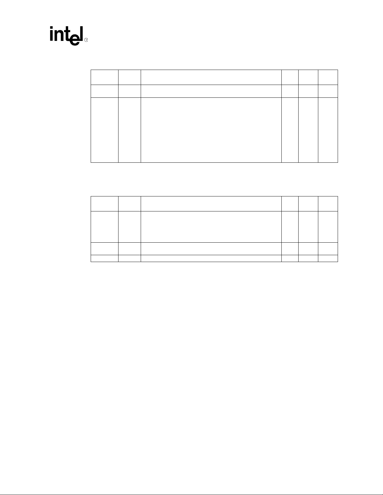
Three CE pins are used to enable and disable the device. A unique CE logic design (see Table 2,
“Chip Enable Truth Table” on page 7) reduces decoder logic typically required for mu lti- chip
designs. External logic is not required when designing a s ingle chip, a dual chip, or a 4-chip
miniature card or SIMM module.
The BYTE# pin allows either x8 or x16 read/writes to the device. BYTE# at logic low selects 8-bit
mode; address A
operation; address A
selects between the low byte and high byte. BYTE# at logic high enables 16-bit
0
becomes the lowest order address and address A0 is not used (don’t care). A
1
device block diagram is shown in Figure 1 on page 2.
When the device is disabled (see Table 2 on page 7) and the R P# pin is at V
enabled. When the RP# pin is at GND, a further po wer-down mode is enabled which minimizes
power consumption and provides write protection during reset. A reset time (t
from RP# switching high until outputs are valid. Likewise, the device has a wake time (t
from RP#-high until writes to the CUI are recognized. W ith RP# at GND, the WSM is reset and the
status register is cleared.
3 Volt Intel StrataFlash memory devices are available in two package types. Both 56-lead TSOP
(Thin Small Outline Package) and BGA (Ball Grid Array Package) s upport all offered densities.
Figure 2 and Figure 3 show the pinouts.
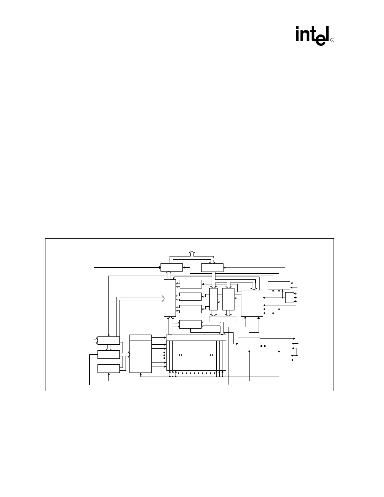
Figure 1. 3 Volt Intel
V
CCQ
32-Mbit: A0- A
64-Mbit: A0 - A
128-Mbit: A0 - A
21
22
23
Input Buffer
Address
Latch
Address
Counter
®
StrataFlash™ Memory Block Diagram
DQ0 - DQ
15
A0- A
2
Y-Decoder
X-Decoder
Output
Buffer
Output
Latch/Multiplexer
128-Mbit: One-hundred
Identifier
Register
Register
Comparator
32-Mbit: Thirty-two
64-Mbit: Sixty-four
128-Kbyte Blocks
Query
Status
Data
Y-Gating
twenty-eight
Input Buffer
Data
Multiplexer
Register
, the standby mode is
CC
) is required
PHQV
V
CE
Logic
STS
CC
BYTE#
CE
CE
CE
WE#
OE#
RP#
V
PEN
V
GND
CC
I/O Logic
Command
Write Buffer
User
Interface
Write State
Machine
Program/Erase
Voltage Switch
0
1
2
PHWL
)
2 Preliminary
Page 9

28F128J3A, 28F640J3A, 28F320J3A
Table 1. Lead Descriptions
Symbol Type Name and Function
A
0
A
1–A23
DQ0–DQ
–
DQ
8
DQ
15
,
CE
0
,
CE
1
CE
2
7
INPUT
INPUT
INPUT/
OUTPUT
INPUT/
OUTPUT
INPUT
RP# INPUT
OE# INPUT
WE# INPUT
OPEN
STS
DRAIN
OUTPUT
BYTE# INPUT
V
PEN
V
CC
INPUT
SUPPLY DEVICE POWER SUPPLY: With VCC ≤ V
OUTPUT
V
CCQ
BUFFER
SUPPLY
GND SUPPLY GROUND: Do not float any ground pins.
NC NO CONNECT: Lead is not internally connected; it may be driven or floated.
DU DON’T USE: Do not drive bal l t o V
BYTE-SELECT ADDRESS: Selects between high and low byte when the device is in x8 mode. This
address is latched during a x8 program cycle. Not used in x16 mode (i.e., the A0 input buffer is turned
off when BYTE# is high).
ADDRESS INPUTS: Inputs for addresses during read and program operations. Addresses are
internally latched during a program cycle.
32-Mbit: A
64-Mbit: A0–A
128-Mbit: A0–A
0–A21
22
23
LOW-BYTE DATA BUS: Inputs data during buffer writes and programming, and inputs commands
during Command User Interface (CUI) writes. Outputs array, query, identifier, or status data in the
appropriate read mode. Floated when the chip is de-selected or the outputs are disabled. Outputs
–DQ0 are also floated when the Write State Machine (WSM) is busy. Check SR.7 (status register
DQ
6
bit 7) to determine WSM status.
HIGH-BYTE DATA BUS: Inputs data during x16 buffer writes and programming operations. Outputs
array, query, or identifier data in the appropriate read mode; not used for status register reads. Floated
when the chip is de-selected, the outputs are disabled, or the WSM is busy.
CHIP ENABLES: Activates the device’s control logic, input buffers, decoders, and sense amplifiers.
When the device is de-selected (see Table 2 on page 7), power reduces to standby levels.
All timing specifications are the same for these three signals. Device selection occurs with the first
edge of CE
CE
0
, CE1, or CE2 that enables the device. Device deselection occurs with the first edge of
0
, CE1, or CE2 that disables the device (see Table 2 on page 7).
RESET/ POWER-DOWN: Resets internal automation and puts the device in power-down mode. RP#high enables normal operation. Exit from reset sets the device to read array mode. When driven low,
RP# inhibits write operations which provides data protection during power transitions.
OUTPUT ENABLE: Activates the device’s outputs through the data buffers during a read cycle. OE# is
active low.
WRITE ENABLE: Controls writes to the Command User Interface, the Write Buffer, and array blocks.
WE# is active low. Addresses and data are lat ched on the rising edge of the WE# pulse.
STATUS: Indicates the status of t he internal state machine. When configured in level mode (default
mode), it acts as a RY/BY# pin. When configured in one of its pulse modes, it can pulse to indicate
program and/or erase completion. For alternate configurations of the STATUS pin, see the
Configurations command. Tie STS to V
with a pull-up resistor.
CCQ
BYTE ENABLE: BYTE# low places the device in x8 mode. All data is then input or output on DQ
, while DQ8–DQ15 float. Address A0 selects between the high and low byte. BYTE# high places
DQ
7
the device in x16 mode, and turns off the A
address.
input buffer. Address A1 then becomes the lowest order
0
ERASE / PROGRAM / BLOCK LOCK ENABLE: For erasing array blocks, programming data, or
configuring lock-bits.
With V
PEN
≤ V
, memory contents cannot be altered.
PENLK
LKO
, all write attempts to the flash memory are inhibited.
OUTPUT BUFFER POWER SUPPLY: This voltage controls the device’s output voltages. To obtain
output voltages compatible with system data bus voltages, connect V
or VIL, leave disconnected
IH
to the system supply voltage.
CCQ
–
0
Preliminary 3
Page 10
28F128J3A, 28F640J3A, 28F320J3A
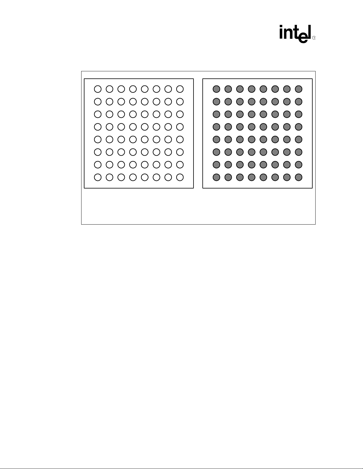
Figure 2. 3 Volt Intel® StrataFlash™ Memory Easy BGA Package
1 2 3 4 5 6 7 8
A
A1A6A8V
B
PENA13VCCA18A22
(1)
A
B
A2GND A9CE0#A14DU A19CE1#
C
A
3A7A10A12A15
DU A20A
D
A4A5A
E
DQ8DQ1DQ9DQ3DQ4DU DQ15STS
RP# DU DU A16A
11
F
BYTE# DQ
G
(2)
A
23
0DQ10DQ11DQ12
A0DQ2V
CCQDQ5DQ6DQ14
DU DU OE#
H
#DU VCCGND DQ13GND DQ7A
CE
2
WE#
24
21
17
(3)
C
D
E
F
G
H
Top View - Ball Side Down Bottom View - Ball Side Up
32 Mbit, 64 Mbit and 128 Mbit: 10 x 13 x 1.2 mm
1.0 mm-ball pitch
NOTES:
1. Address A
2. Address A
3. Address A
4. Don’t Use (DU) pins refer to pins that should not be connected
is only valid on 64-Mbit densities and above, otherwise, it is a no connect (NC)
22
is only valid on 128-Mbit densities and above, otherwise, it is a no connect (NC)
23
is only valid on 256-Mbit densities and above, otherwise, it is a no connect (NC)
24
8 7 6 5 4 3 2 1
(1)
A
A18VCCA13V
22
CE1#A19DU A14CE0#A9GND A
A21A20DU A15A12A10A7A
A17A16DU
STS DQ
DU DQ4DQ3DQ9DQ1DQ
15
PENA8A6A1
DU RP# A
2
3
11A5A4
8
OE# DU DU DQ12DQ11DQ10DQ0BYTE#
WE# DQ
A
14DQ6DQ5VCCQDQ2A0A23
(3)
DQ7GND DQ13GND VCCDU CE2#
24
(2)
0667-02
4 Preliminary
Page 11
28F128J3A, 28F640J3A, 28F320J3A
Figure 3. 3 Volt Intel® StrataFlash™ Memory 56-Lead TSOP (32/64/128 Mbit) Offers an Easy
Migration from the 32-Mbit Intel StrataFlash Component (28F320J5) or the 16-Mbit
FlashFile™ Component (28F160S3)
28F160S3
NC
CE
1
NC
A
20
A
19
A
18
A
17
A
16
V
CC
A
15
A
14
A
13
A
12
CE
0
V
PP
RP#
A
11
A
10
A
9
A
8
GND
A
7
A
6
A
5
A
4
A
3
A
2
A
1
28F320J5
NC
CE
1
A
21
A
20
A
19
A
18
A
17
A
16
(4)
V
CC
A
15
A
14
A
13
A
12
CE
0
V
PEN
RP#
A
11
A
10
A
9
A
8
GND
A
7
A
6
A
5
A
4
A
3
A
2
A
1
3 Volt Intel
StrataFlash
Memory
32/64/128M
(1)
A
22
CE
1
A
21
A
20
A
19
A
18
A
17
A
16
V
CC
A
15
A
14
A
13
A
12
CE
0
V
PEN
RP#
A
11
A
10
A
9
A
8
GND
A
7
A
6
A
5
A
4
A
3
A
2
A
1
1
2
3
4
5
6
7
8
9
10
11
12
13
14
15
16
17
18
19
20
21
22
23
24
25
26
27
28
Intel® StrataFlash™ Memory
56-Lead TSOP
Standard Pinout
14 mm x 20 mm
Top View
3 Volt Intel
StrataFlash
Memory
32/64/128M
56
55
54
53
52
51
50
49
48
47
46
45
44
43
42
41
40
39
38
37
36
35
34
33
32
31
30
29
(3)
A
24
WE#
OE#
STS
DQ
15
DQ
7
DQ
14
DQ
6
GND
DQ
13
DQ
5
DQ
12
DQ
4
V
CCQ
GND
DQ
11
DQ
3
DQ
10
DQ
2
V
CC
DQ
9
DQ
1
DQ
8
DQ
0
A
0
BYTE#
(2)
A
23
CE
2
Highlights pinout changes
NOTES:
exists on 64-, 128- and 256-Mbit densities. On 32-Mbit densities this pin is a no-connect (NC).
1. A
22
exists on 128-Mbit densities. On 32- and 64-Mbit densities this pin is a no-connect (NC).
2. A
23
exists on 256-Mbit densities. On 32-, 64- and 128-Mbit densities this pin is a no-connect (NC) .
3. A
24
= 5 V ± 10% for the 28F640J5/28F320J5.
4. V
CC
28F320J5
NC
WE#
OE#
STS
DQ
15
DQ
7
DQ
14
DQ
6
GND
DQ
13
DQ
5
DQ
12
DQ
4
V
CCQ
GND
DQ
11
DQ
3
DQ
10
DQ
2
(4)
V
CC
DQ
9
DQ
1
DQ
8
DQ
0
A
0
BYTE#
NC
CE
2
28F160S3
WP#
WE#
OE#
STS
DQ
15
DQ
7
DQ
14
DQ
6
GND
DQ
13
DQ
5
DQ
12
DQ
4
V
CC
GND
DQ
11
DQ
3
DQ
10
DQ
2
V
CC
DQ
9
DQ
1
DQ
8
DQ
0
A
0
BYTE#
NC
NC
0667-03
Preliminary 5
Page 12

28F128J3A, 28F640J3A, 28F320J3A
2.0 Principles of Operation
The Intel StrataFlash memory devices include an on-chip WSM to manage block erase, program,
and lock-bit configuration functions. It allows for 100% TTL-level control inputs, fixed power
supplies during block erasure, program, lock-bit configuration, and minimal processor overhead
with RAM-like interface timings.
After initial device power-up or return from reset/power-down mode (see Section 3.0, “Bus
Operations” on page 7), the device defaults to read array mode. Manipulation of external memory
control pins allows array read, standby, and output disable operations.
Read array, s tatus register, query, and identifier codes can be accessed through the CUI (Comma nd
User Interface) independent of the V
erasure, programming, and lock-bit configuration. All functions associated with altering memory
contents—block erase, program, lock-bit configuration—are accessed via the CUI and verified
through the status register.
Commands are written using standard micro-processor write timings. The CUI contents serve as
input to the WSM, which controls the block erase, program, and lock-bit configuration. The
internal algorithms are regulated by the WSM, including pulse repetition, internal verification, and
margining of data. Addresses and data are internally latched during program cycles.
voltage. V
PEN
PENH
on V
enables successful block
PEN
Interface software that initiates and polls progress of block erase, program, and lock-bit
configuration can be stored in any block. This code is copied to and executed from system RAM
during flash memory updates. After successful completion, reads are again possible via the Read
Array command. Block erase suspend allows system software to suspend a block erase to read or
program dat a from/to any other block. Program suspend allows system so ftware to suspe nd a
program to read data from any other flash memory array location.
2.1 Data Protection
Depending on the application, the system designer may choose to make the V
(available only when memory block erases, programs, or lock-bit configurations are required) or
hardwired to V
optimization of the processor-memory interface.
When V
PEN
≤ V
word program, and lock-bit configuration command sequences provide protection from unwanted
operations even when V
below the write lockout voltage V
provides additional protection from inadvertent code or data alteration by gating erase and program
operations.
. The device accommodates either design practice and encourages
PENH
, memory contents cannot be altered. The CUI’s two-step block erase, byte/
PENLK
is applied to V
PENH
switchable
PEN
. All program functions are disabled when VCC is
PEN
or when RP# is VIL. The device’s block locking capability
LKO
6 Preliminary
Page 13
3.0 Bus Operations
The local CPU reads and writes flash memory in-system. All bus cycles to or from the flash
memory conform to standard microprocessor bus cycles.
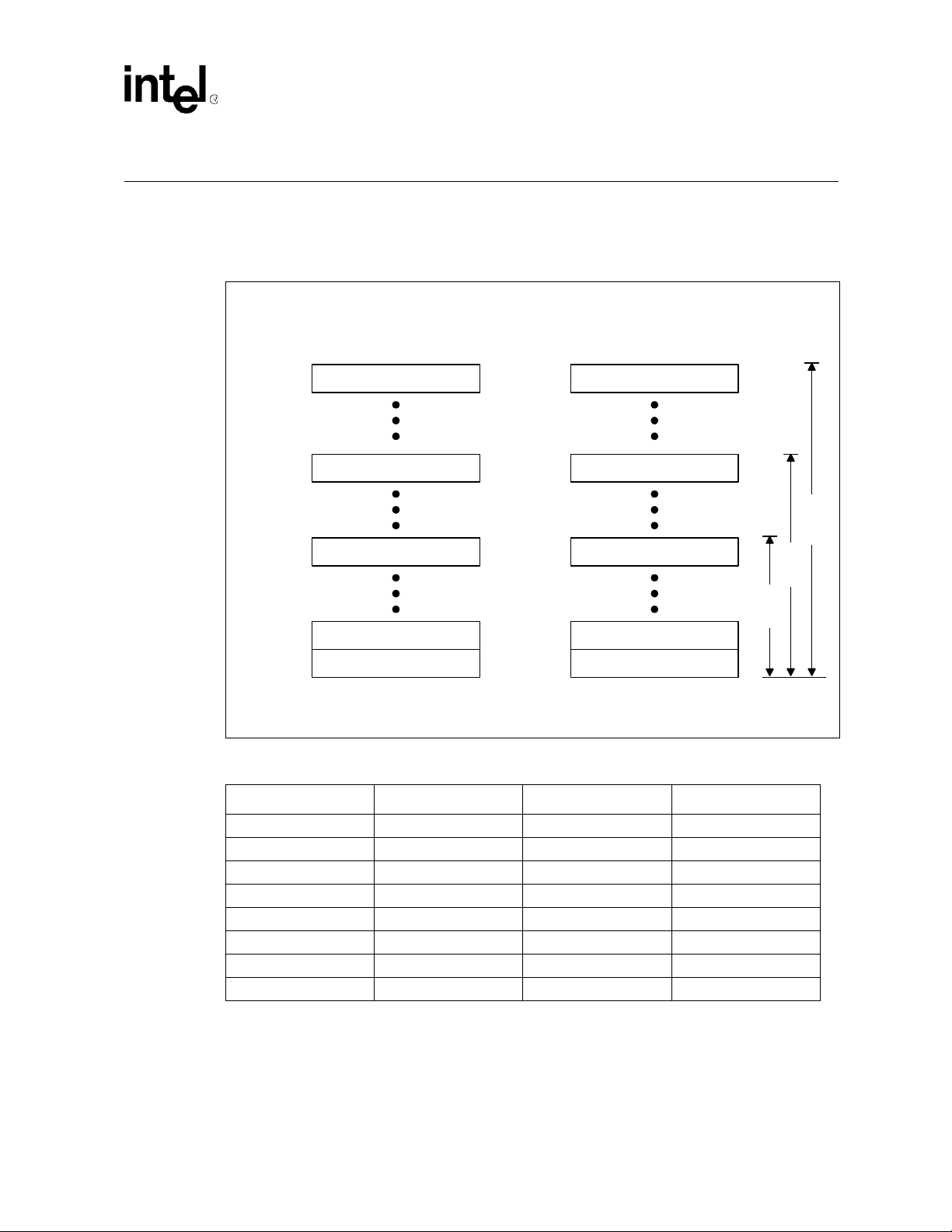
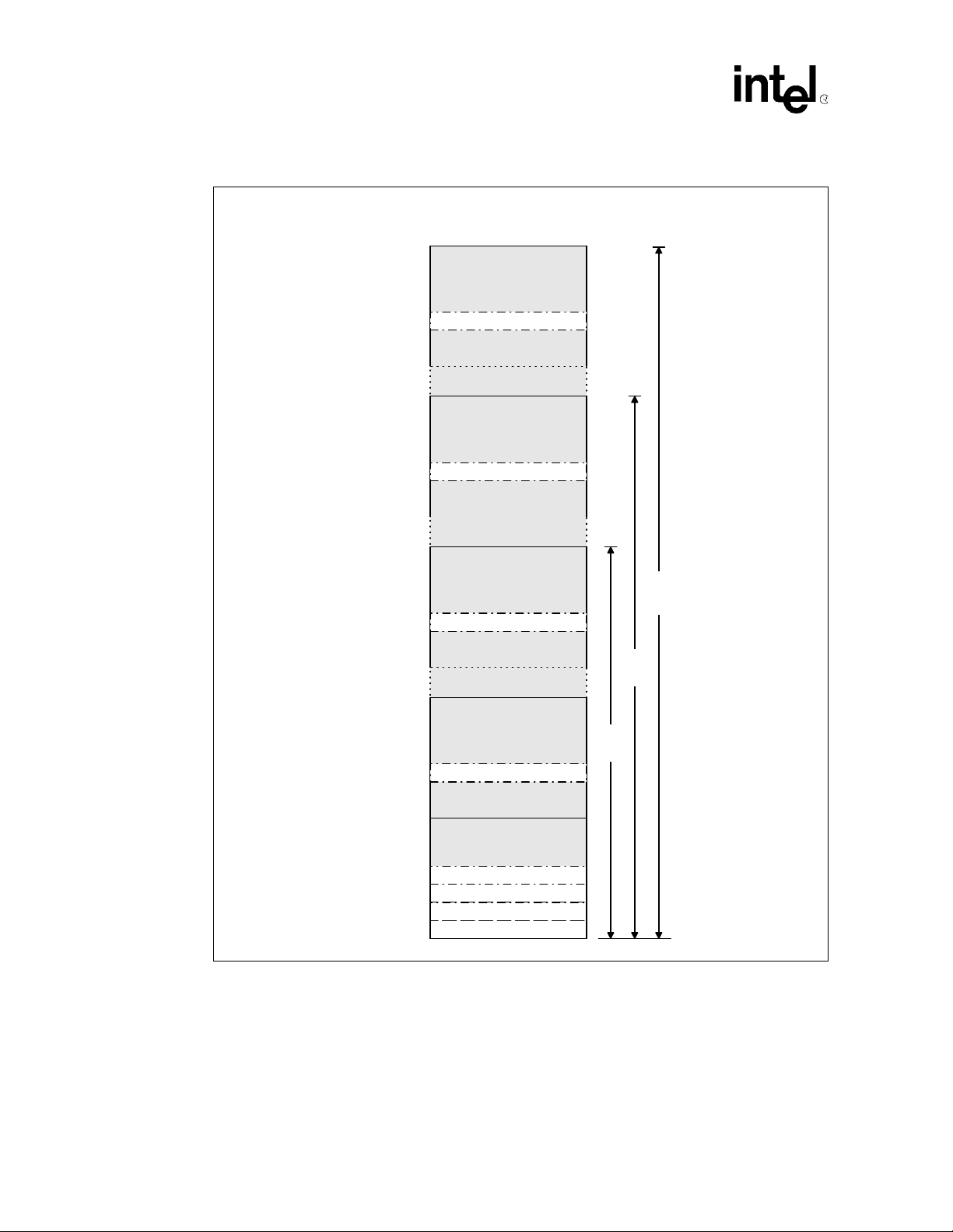
Figure 4. Memory Map
28F128J3A, 28F640J3A, 28F320J3A
A [23-0]:128 Mbit
A [22-0]: 64 Mbit
A [21-0]: 32 Mbit
FFFFFF
FE0000
7FFFFF
7E0000
3FFFFF
3E0000
03FFFF
020000
01FFFF
000000
Byte-Wide (x8) Mode
128-Kbyte Block
128-Kbyte Block
128-Kbyte Block
128-Kbyte Block
128-Kbyte Block
127
A [23-1]: 128 Mbit
A [22-1]: 64 Mbit
A [21-1]: 32 Mbit
7FFFFF
7F0000
63
31
3FFFFF
3F0000
1FFFFF
1F0000
64-Kword Block
64-Kword Block
64-Kword Block
127
63
31
128-Mbit
64-Mbit
1
0
01FFFF
010000
00FFFF
000000
64-Kword Block
64-Kword Block
1
0
32-Mbit
Word Wide (x16) M ode
Table 2. Chip Enable Truth Table
CE
2
V
IL
V
IL
V
IL
V
IL
V
IH
V
IH
V
IH
V
IH
NOTE: For single-chip applications, CE2 and CE1 can be strapped to GND.
CE
V
V
V
V
V
V
V
V
1
IL
IL
IH
IH
IL
IL
IH
IH
CE
V
V
V
V
V
V
V
V
0
IL
IH
IL
IH
IL
IH
IL
IH
DEVICE
Enabled
Disabled
Disabled
Disabled
Enabled
Enabled
Enabled
Disabled
Preliminary 7
Page 14

28F128J3A, 28F640J3A, 28F320J3A
3.1 Read
Information can be read from any block, query, identifier codes, or status register i ndependent of
PEN
voltage.
the V
Upon initial device power-up or after exit from reset/power-down mode, the device automatically
resets to read array mode. Otherwise, write the appropriate read m ode command (Read Array, Read
Query , Read Identifier Codes, or Read St atus Register) to the CUI. Six control pins dictate the data
flow in and out of the component: CE
enabled (see Table 2, “Chip Enable Truth Table” on page 7), and OE# must be driven active to
obtain data at the outputs. CE
(see Table 2), select the memory device. OE# is the data output (DQ
active, drives the selected memory data onto the I/O bus. WE# must be at V
When reading information in read array mode, the device defaults to asynchronous page mode.
This mode provides high data transfer rate for memory subsystems. In this state, data is internally
read and stored in a high-speed page buffer. A
four words or eight bytes. Asynchronous word/byte mode is supported with no additional
commands required.
3.2 Output Disable
, CE1, CE2, OE#, WE#, and RP#. The device must be
0
, CE1, and CE2 are the device selection controls and, when enabled
0
addresses data in the page buf fer. The page size is
2:0
–DQ15) control and, when
0
IH
.
With OE# at a logic-high level (VIH), the device outputs are disabled. Output pins DQ0–DQ15 are
placed in a high-impedance state.
3.3 Standby
CE0, CE1, and CE2 can disable the device (see Table 2) and place it in standby mode which
substantially reduces device power consumption. DQ
impedance state independent of OE#. If deselected during block erase, program, or lock-bit
configuration, the WSM continues functioning, and consuming active power until the operation
completes.
3.4 Reset/Power-Down
RP# at VIL initiates the reset/power-down mode.
In read modes, RP#-low deselects the memory , places output drivers in a high-impedance state, and
turns off numerous int ernal circu i ts. R P# mus t be held l o w for a mi n imum o f t
required after return from reset mode until initial memory access outputs are valid. After this wakeup interval, normal operation is restored. The CUI is reset to read array mode and status register is
set to 80H.
During block erase, program, or lock-bit configuration modes, RP#-low will abort the operation. In
default mode, STS transitions low and remains low for a maximum time of t
reset operation is complete. Memory contents being altered are no longer valid; the data may be
partially corrupted after a program or partially altered after an erase or lock-bit configuration. Time
t
is required after RP# goes to logic-high (VIH) before another command can be written.
PHWL
–DQ15 outputs are placed in a high-
0
. Time t
PLPH
+ t
PLPH
PHRH
is
PHQV
until the
8 Preliminary
Page 15

As with any automated device, it is important to assert RP# during system reset. When the system
comes out of reset, it expects to read from the flash memory. Automated flash memories provide
status information when accessed during block erase, program, or lock-bit configuration modes. If
a CPU reset occurs with no flash memory reset, proper i nitialization may not occur because the
flash memory may be providi ng status information instead of array data. Intel
allow proper initialization following a system reset thr ough the use of the RP# input. In this
application, RP# is controlled by the same RESET# signal that resets the system CPU.
3.5 Read Query
The read query operation outputs block status information, CFI (Common Flash Interface) ID
string, system interface information, device geometry information, and Intel-specific extended
query information.
3.6 Read Identifier Codes
The read identifier codes operation outputs the manufacturer code, device code and the block lock
configuration codes for each block (see Figure 5 on page 10). Using the manufacturer and device
codes, the system CPU can automatically match the device with its proper algo rithms. The block
lock configuration codes identify locked and unlo cked bl ocks .
28F128J3A, 28F640J3A, 28F320J3A
®
Flash memories
3.7 Write
Writing commands to the CUI enables reading of device data, query, identifier codes, inspection
and clearing of the status register, and, when V
configuration.
The Block Erase command requires appropriate command data and an address within the block to
be erased. The Byte/Word Program command requires the command and address of the location to
be written. Set Block Lock-Bit commands require the command and block within the device to be
locked. The Clear Block Lock-Bits command req uires the co mmand and add res s within the d evice.
The CUI does not occupy an addressable memory location. It is written when the device is enabled
and WE# is active. The address and data needed t o execute a command are latched on the rising
edge of WE# or the first edge of CE
, CE1, or CE2 that disables the device (see Table 2). Standard
0
microprocessor write timings are used.
4.0 Command Definitions
When the V
codes, or blocks are enabled. Placing V
and lock-bit configuration operations.
Device operations are selected by writing specific commands into the CUI. Tab le 4 defines these
commands.
voltage ≤ V
PEN
, only read operations from the status register, query, identifier
PENLK
PENH
PEN
on V
= V
PEN
, block erasure, program, and lock-bit
PENH
additionally enables block erase, program,
Preliminary 9
Page 16
28F128J3A, 28F640J3A, 28F320J3A
Figure 5. Device Identifier Code Memory Map
Word
Address
7FFFFF
7F0003
7F0002
7F0000
7EFFFF
3FFFFF
3F0003
3F0002
3F0000
3EFFFF
1F0003
1F0002
1F0000
1EFFFF
01FFFF
010003
010002
010000
00FFFF
000004
000003
000002
000001
000000
A[23-1]: 128 Mbit
A[22-1]: 64 Mbit
A[21-1]: 32 Mbit
Block 127
Reserved for Future
Implementation
Block 127 Lock Configuration
Reserved for Future
Implementation
(Blocks 64 through 126)
Block 63
Reserved for Future
Implementation
Block 63 Lock Configuration
Reserved for Future
Implementation
(Blocks 32 through 62)
Block 31
Reserved for Future
Implementation
Block 31 Lock Configuration
Reserved for Future
Implementation
(Blocks 2 through 30)
Block 1
Reserved for Future
Implementation
Block 1 Lock Configuration
Reserved for Future
Implementation
Block 0
Reserved for Future
Implementation
Block 0 Lock Configuration
Device Code
Manufacturer Code
128 Mbit
64 Mbit
32 Mbit
NOTE: A
is not used in either x8 or x16 modes when obtaining these identifier codes. Data is always given on the low byte in
0
x16 mode (upper byte contains 00h).
0606-06a
10 Preliminary
Page 17

T a ble 3. Bus Operations
28F128J3A, 28F640J3A, 28F320J3A
Mode Notes RP# CE
Read Array 4,5,6 V
Enabled V
IH
0,1,2
(1)
OE#
Output Disable VIH Enabled V
Standby V
Reset/Power-Down
Mode
Disabled X X X X High Z X
IH
V
IL
X X X X X High Z High Z
Read Identifier Codes VIH Enabled V
Read Query VIH Enabled V
Read Status (WSM off) VIH Enabled V
Read Status (WSM on) VIH Enabled V
Write 6,10,11 V
Enabled V
IH
NOTES:
1. See Table 2 for valid CE configurations.
2. OE# and WE# should never be enabled simultaneously.
3. DQ refers to DQ
4. Refer to DC Characteristics. When V
5. X can be V
V
PENLK
6. In default mode, STS is V
or VIH for control and address pins, and V
IL
and V
PENH
configuration algorithms. It is V
programming inactive), program suspend mode, or reset/power-down mode.
7. High Z will be V
8. See Section 3.6 for read identifier code data.
if BYTE# is low and DQ0–DQ15 if BYTE# is high.
0–DQ7
PEN
voltages.
when the WSM is executing internal block erase, program, or lock-bit
OL
when the WSM is not busy, in block erase suspend mode (with
OH
with an external pull-up resistor.
OH
9. See Section 4.2 for read query data.
10.Command writes involving block erase, program, or lock-bit configuration are reliably executed when V
and VCC is within specification.
V
PENH
11.Refer to Table 4 for valid D
during a write operation.
IN
IL
IH
IL
IL
IL
IL
IH
≤ V
(2)
(2)
WE#
V
IH
V
IH
V
IH
V
IH
V
IH
Address V
PEN
XX D
XX High Z X
See
Figure 5
See
Table 7
X Note 8 High Z
X Note 9 High Z
XX D
DQ
V
IH
V
IL
, memory contents can be read, but not altered.
PENLK
XX
XV
or V
PENLK
PENH
PENH
for V
DQ
15–8
DQ
6–0
. See DC Characteristics for
PEN
(3)
DQ
OUT
OUT
= D
7
= High Z
= High Z
D
IN
OUT
STS
(default
mode)
High Z
X
PEN
(7)
(7)
(7)
(7)
=
Preliminary 11
Page 18

28F128J3A, 28F640J3A, 28F320J3A
Data
(5,6)
(1)
Oper
(3)
Addr
(4)
Data
Table 4. Intel® StrataFlash™ Memory Command Set Definitions
Command
Scalable or
Basic
Command
(2)
Set
Bus
Cycles
Req’d.
Notes First Bus Cycle Second Bus Cycle
Oper
(3)
Addr
(4)
Read Array SCS/BCS 1 Write X FFH
Read Identifier Codes SCS/BCS ≥ 2 7 Write X 90H Read IA ID
Read Query SCS ≥ 2 Write X 98H Read QA QD
Read Status Register SCS/BCS 2 8 Write X 70H Read X SRD
Clear Status Register SCS/BCS 1 Write X 50H
Write to Buffer SCS/BCS > 2
9, 10,
11
Write BA E8H Write BA N
40H
Word/Byte Program SCS/BCS 2 12,13 Write X
or
Write PA PD
10H
Block Erase SCS/BCS 2 11,12 Write BA 20H Write BA D0H
Block Erase, Program
Suspend
Block Erase, Program
Resume
SCS/BCS 1 12,14 Write X B0H
SCS/BCS 1 12 Write X D0H
Configuration SCS 2 Write X B8H Write X CC
Set Block Lock-Bit SCS 2 Write X 60H Write BA 01H
Clear Block Lock-Bits SC S 2 15 Write X 60H Write X D0H
Protection Program 2 Write X C0H Write PA PD
(5,6)
NOTES:
1. Commands other than those shown above are reserved by Intel for future device implementations and
should not be used.
2. The Basic Command Set (BCS) is the same as the 28F008SA Command Set or Intel Standard Command
Set. The Scalable Command Set (SCS) is also referred to as the Intel Extended Command Set.
3. Bus operations are defined in Table 3.
4. X = Any valid address within the device.
BA = Address within the block.
IA = Identifier Code Address: see Figure 5 and Table 15.
QA = Query database Address.
PA = Address of m e mo ry location to be programmed.
RCD = Data to be written to the read configuration register. This data is presented to the device on A
other address inputs are ignored.
16-1
; all
5. ID = Data read from Identifier Codes.
QD = Data read from Query database.
SRD = Data read from status register. See Table 16 for a description of the status register bits.
PD = Data to be programmed at location P A . Data is latched on the rising edge of WE#.
CC = Configuration Code.
6. The upper byte of the data bus (DQ
7. Following the Read Identifier Codes command, read operations access manufacturer, device and block lock
) during command writes is a “Don’t Care” in x16 operation.
8–DQ15
codes. See Section 4.3 for read identifier code data.
8. If the WSM is running, only DQ
impedance state.
is valid; DQ
7
and DQ6–DQ0 float, which places them in a high-
15–DQ8
9. After the Write to Buffer command is issued check the X SR to make sure a buffer is available for writing.
12 Preliminary
Page 19

10.The number of bytes/words to be written to the Write Buffer = N + 1, where N = byte/word count argument.
Count ranges on this device for byte mode are N = 00H to N = 1FH and for word mode are N = 0000H t o N =
000FH. The third and consecutive bus cycles, as determined by N, are for writing data into the Write Buffer.
The Confirm command (D0H) is expected after exactly N + 1 write cycles; any other command at that point in
the sequence aborts the write to buffer operation. Please see Figure 7, “Write to Buffer Flowchart” on
page 30 for additional information.
11.The write to buffer or erase operation does not begin until a Confirm command (D0h) is issued.
12.Attempts to issue a block erase or program to a locked block.
13.Either 40H or 10H are recognized by the WSM as the byte/word program setup.
14.Program suspends can be issued after either the Write-to-Buffer or Word-/Byte-Program operation is
initiated.
15.The clear block lock-bits operation simultaneously clears all block lock-bits.
4.1 Read Array Command
Upon initial device power-up and after exit from reset/power-down mode, the device defaults to
read array mode. The read configuration register defaults to asynchronous read page mode. The
Read Array command also causes the device to enter read array mode. The device rem ains enabled
for reads until another command is written. Once the internal WSM has started a block erase,
program, or lock-bit configuration, the device will not recognize the Read Array command until
the WSM completes its operation unless the WSM is suspended via an Erase or Program Suspend
command. The Read Array command functions independently of the V
28F128J3A, 28F640J3A, 28F320J3A
voltage.
PEN
4.2 Read Query Mode Command
This section defines the data structure or “database” returned by the Common Flash Interface (CFI)
Query command. System software should pars e this structure to gain critical information such as
block size, density, x8/x16, and electrical specifications. Once this information has been obtained,
the software will know which command sets to use to enable flash writes, block erases, and
otherwise control the flash component. The Query is part of an overall specification for multiple
command set and control interface descriptions called Common Flash Interface, or CFI.
4.2.1 Query Structure Output
The Query “database” allows system software to gain information for controlling the flash
component. This section describes the device’s CFI-compliant interface that allows the host system
to access Query data.
Query data are always presented on the lowest-order data outputs (DQ
offset value is the address relative to the maximum bus width supported by the device. On this
family of devices, the Query table device starting address is a 10h, which is a word address for x16
devices.
For a word-wide (x16) device, the first two bytes of the Query structure, “Q” and “R” in ASCII,
appear on the low byte at word addresses 10h and 11h. This CFI-compliant device outputs 00H
data on upper bytes. Thus, the device outputs ASCII “Q” in the low byte (DQ
high byte (DQ
At Query addresses containing two or more bytes of information, the least significant data byte is
presented at the lower address, and the mos t s ignifican t data byte is presented at the higher address.
8–15
).
) only. The numerical
0–7
) and 00h in the
0–7
Preliminary 13
Page 20

28F128J3A, 28F640J3A, 28F320J3A
In all of the following tables, addresses and data are represented in hexadecimal notation , so the
“h” suffix has been dropped. In addition, since the upper byte of word-wide devices is always
“00h,” the leading “00” has been dropped from the table notation and only the lower byte value is
shown. Any x16 device outputs can be assumed to have 00h on the upper byte in this mode.
Table 5. Summary of Query Structure Output as a Function of Device and Mode
Device
Type/
Mode
x16 device 10h 10: 0051 “Q” 20: 51 “Q”
x16 mode 11: 0052 “R” 21: 00 “Null”
x16 device 20: 51 “Q”
x8 mode N/A
NOTE:
1. The system must drive the lowest order addresses to access all the device’s array data when the device is
configured in x8 mode. Therefore, word addressing, where these lower addresses are not toggled by the
system, is "Not Applicable" for x8-configured devices.
Query start location in
maximum device bus
width addresses
(1)
Query data with maximum
device bus width addressing
Hex
Offset
12: 0059 “Y” 22: 52 “R”
Hex
Code
N/A
ASCII
Value
(1)
Hex
Offset
21: 51 “Q”
22: 52 “R”
Query data with byte
addressing
Hex
Code
ASCII
Value
T able 6. Example of Query Structure Output of a x16- and x8-Capable Device
Word Addressing Byte Addressing
Offset Hex Code Value Offset Hex Code Value
A
15–A0
0010h 0051 “Q” 20h 51 “Q”
0011h 0052 “R” 21h 51 “Q”
0012h 0059 “Y” 22h 52 “R”
0013h P_ID
0014h P_ID
0015h P
0016h P
0017h A_ID
0018h A_ID
... ... ... ... ... ...
LO
D15–D
0
LO
HI
HI
LO
HI
PrVendor 23h 52 “R”
ID # 24h 59 “Y”
PrVendor 25h 59 “Y”
TblAdr 26h P_ID
AltVendor 27h P_ID
ID # 28h P_ID
A7–A
0
4.2.2 Query Structure Overview
The Query command causes the flash component to display the Common Flash Interface (CFI)
Query structure or “database.” The structure sub-s ections and address locations are summarized
below. See AP-646 Common Flash Interface (CFI) and Command Sets (order number 292204) for
a full description of CF I.
The following sections describe the Query structure sub-sections in detail.
LO
LO
HI
D7–D
0
PrVendor
ID #
ID #
14 Preliminary
Page 21

28F128J3A, 28F640J3A, 28F320J3A
Table 7. Query Structure
Offset Sub-Section Name Description
00h Manufacturer Code
01h Device Code
(2)
(BA+2)h
04-0Fh Reserved Reserved for Vendor-Specific Information
10h CFI Query Identification String Reserved for Vendor-Specific Information
1Bh System Interface Information Command Set ID and Vendor Data Offset
27h Device Geometry Definition Flash Device Layout
(3)
P
NOTES:
1. Refer to the Query St ructure Output section and offset 28h for the detailed definition of offset address as a
function of device bus width and mode.
2. BA = Block Address beginning location (i.e., 02000h is block 2’s beginning loc ation when the block size is
128 Kbyte).
3. Offset 15 defines “P” which points to the Primary Intel-Specific Extended Query Table.
(1)
Block Status Register Block-Specific Information
Primary Intel-Specific Extended
Query Table
4.2.3 Block Status Register
The block status register indicates whether an erase oper ation comp leted succes sfully or wh ethe r a
given block is locked or can be accessed for flash program/erase operations.
T a ble 8. Block Status Register
Offset Length Description Address Value
(BA+2)h
(1)
1 Block Lock Status Register BA+2: --00 or --01
BSR.0 Block Lock Status
0 = Unlocked
1 = Locked
BSR 1–7: Reserved for Fu tu re U s e BA+2: (bit 1–7): 0
Vendor-Defined Additional Information Specific to the
Primary Vendor Algorithm
BA+2: (bit 0): 0 or 1
NOTE:
1. BA = The beginning location of a Block Address (i.e., 008000h is block 1’s (64-KB block) beginning location
in word mode).
4.2.4 CFI Query Identification String
The CFI Query Identification String provides verification that the component supports the
Common Flash Interface specification.
vendor-specified command set(s).
T a ble 9. CFI Identification
Offset Length Description Add.
10h 3 Query-unique ASCII string “QRY”
13h 2 Primary vendor command set and control interface ID code. 13: --01
16-bit ID code for vendor-specified algorithms 14: --00
15h 2 Extended Query Table primary algorithm address 15: --31
Preliminary 15
It also indicates the specification version and supported
Hex
Code
10 --51 “Q”
11: --52 “R”
12: --59 “Y”
16: --00
Value
Page 22

28F128J3A, 28F640J3A, 28F320J3A
T able 9. CFI Identification
Offset Length Description Add.
17h 2 Alternate vendor command set and control interface ID code. 17 : --00
0000h means no second vendor-specified algorithm exists 18: --00
19h 2 Secondary algorithm Extended Query Table address. 19: --00
0000h means none exists 1A: --00
4.2.5 System Interface Information
The following device information can optimize system interface software.
Table 10. System Interface Information
Offset Length Description Add.
V
logic supply minimum program/erase voltage
1Bh 1
1Ch 1
1Dh 1
1Eh 1
1Fh 1 “n” such that typical single word program time-out = 2
20h 1 “n” such that typical max. buffer write time-out = 2
21h 1 “n” such that typical block erase time-out = 2
22h 1 “n” such that typical full chip erase time-out = 2
23h 1
24h 1 “n” such that maximum buffer write time-out = 2
25h 1 “n” such that maximum block erase time-out = 2
26h 1 “n” such that maximum chip erase time-out = 2
CC
bits 0–3 BCD 100 mV
bits 4–7 BCD volts
logic supply maximum program/erase voltage
V
CC
bits 0–3 BCD 100 mV
bits 4–7 BCD volts
[programming] supply minimum program/erase voltage
V
PP
bits 0–3 BCD 100 mV
bits 4–7 HEX volts
V
[programming] supply maximum program/erase voltage
PP
bits 0–3 BCD 100 mV
bits 4–7 HEX volts
“n” such that maximum word program time-out = 2
typical
Hex
Hex
Value
Value
Code
Code
1B: --27 2.7 V
1C: --36 3.6 V
1D: --00 0.0 V
1E: --00 0.0 V
n
µs 1F: --07 128 µs
n
µs 20: --07 128 µs
n
ms 21: --0A 1 s
n
ms 22: --00 NA
n
times
n
times typical 24: --04 2 ms
n
times typical 25: --04 16 s
n
times typical 26: --00 NA
23: --04 2 ms
16 Preliminary
Page 23

4.2.6 Device Geometry Definition
This field provides critical details of the flash device geometry.
T a ble 11. Device Geometry Definition
Offset Length Description
27h 1 “n” such that device size = 2
28h 2 Flash device interface: x8 async x16 async x8/x16 async 28: --02
28:00, 29:00 28:01,29:00 28:02,29:00 29: --00
2Ah 2 “n” such that maximum number of bytes in write buffer = 2
Number of erase block regions within device:
1. x = 0 means no erase blocking; the device erases in “bulk”
2Ch 1
2Dh 4
2. x specifies the number of device or partition regions with one or
more contiguous same-size erase blocks
3. Symmetrically blocked partitions have one blocking region
4. Partition size = (total blocks) x (individual block size)
Erase Block Region 1 Information 2D:
bits 0–15 = y, y+1 = number of identical-size erase blocks 2E:
bits 16–31 = z, region erase block(s) size are z x 256 bytes 2F:
28F128J3A, 28F640J3A, 28F320J3A
n
in number of bytes 27:
n
Code See Table
Below
x8/
x16
2A: --05 32
2B: --00
2C: --01 1
30:
Device Geometry Definition
Address 32 Mbit 64 Mbit 128 Mbit
27: --16 --17 --18
28: --02 --02 --02
29: --00 --00 --00
2A: --05 --05 --05
2B: --00 --00 --00
2C: --01 --01 --01
2D: --1F --3F --7F
2E: --00 --00 --00
2F: --00 --00 --00
30: --02 --02 --02
Preliminary 17
Page 24

28F128J3A, 28F640J3A, 28F320J3A
4.2.7 Primary-Vendor Specific Extended Query Table
Certain flash features and commands are optional. The Primary Vendor-Sp ecific Extended Query
table specifies this and other similar information.
Table 12. Primary Vendor-Specific Extended Query
(1)
Offset
P = 31h
(P+0)h 3 Primary extended query table 31: --50 “P”
(P+1)h Unique ASCII string “PRI” 32: --52 “R”
(P+2)h 33: --49 “I”
(P+3)h 1 Major version number, ASCII 34: --31 “1”
(P+4)h 1 Minor version number, ASCII 35: --31 “1”
(P+5)h
(P+6)h
(P+7)h
(P+8)h
(P+9)h 1
(P+A)h
(P+B)h
(P+C)h 1
(P+D)h 1
Length
4
2
(Optional Flash Features and Commands)
Optional feature and command support (1=yes, 0=no) 36: --0A
bits 9–31 are reserved; undefined bits are “0.” If bit 31 is 37: --00
“1” then another 31 bit field of optional features follows at 38: --00
the end of the bit-30 field. 39: --00
bit 0 Chip erase supported bit 0 = 0 No
bit 1 Suspend erase supported bit 1 = 1 Yes
bit 2 Suspend program supported bit 2 = 1 Yes
bit 3 Legacy lock/unlock supported bit 3 = 1
bit 4 Queued erase supported bit 4 = 0 No
bit 5 Instant Individual block locking supported bit 5 = 0 No
bit 6 Protection bits supported bit 6 = 1 Yes
bit 7 Page-mode read supported bit 7 = 1 Yes
bit 8 Synchronous read supported bit 8 = 0 No
Supported functions after suspend: read Array, Status,
Query
Other supported operations are:
bits 1–7 reserved; undefined bits are “0”
bit 0 Program supported after erase suspend bit 0 = 1 Yes
Block status register mask 3B: --01
bits 2–15 are Reserved; undefined bits are “0” 3C: --00
bit 0 Block Lock-Bit Status register active bit 0 = 1 Yes
bit 1 Block Lock-Down Bit Status active bit 1 = 0 No
logic supply highest performance program/erase
V
CC
voltage
bits 0–3 BCD value in 100 mV
bits 4–7 BCD value in volts
optimum program/erase supply voltage
V
PP
bits 0–3 BCD value in 100 mV
bits 4–7 HEX value in volts
Description
Add.
3A: --01
3D: --33 3.3 V
3E: --00 0.0 V
Hex
Code
(1)
Value
Yes
(1)
NOTE:
1. Future devices may not support the described “Legacy Lock/Unlock” function. Thus bit 3 would have a value
of “0.”
18 Preliminary
Page 25
T a ble 13. Protection Register Information
(1)
Offset
P = 31h
(P+E)h 1
(P+F)h
(P+10)h
(P+11)h
(P+12)h
NOTE:
1. The variable P is a pointer which is defined at CFI offset 15h.
Length
4
(Optional Flash Features and Commands)
Number of Protection register fields in JEDEC ID space.
“00h,” indicates that 256 protection bytes are available
Protection Field 1: Protection Description
This field describes user-available One Time Programmable
(OTP) protection register bytes. Some are pre-programmed
with device-unique serial numbers. Others are userprogrammable. Bits 0-15 point to the protection register lock
byte, the section’s first byte. The following bytes are factory
pre-programmed and user-programmable.
bits 0-7 = Lock/bytes JEDEC-plane physical low address
bits 8-15 = Lock/bytes JEDEC-plane physical high address
bits 16-23 = “n” such that 2
bits 24-31 = “n” such that 2
T a ble 14. Burst Read Information
(1)
Offset
P = 31h
(P+13)h 1
(P+14)h 1
(P+15)h Reserved for future use 46:
Length
(Optional Flash Features and Commands)
Page Mode Read capability
bits 0–7 = “n” such that 2
of read-page bytes. See offset 28h for device word width to
determine page-mode data output width. 00h indicates no
read page buffer.
Number of synchronous mode read configuration fields that
follow. 00h indicates no burst capability.
28F128J3A, 28F640J3A, 28F320J3A
Description
n
= factory pre-programmed bytes
n
= user-programmable bytes
Description
n
HEX value represents the number
Add.
Add.
Hex
Hex
Value
Value
Code
3F: --01 01
40: --00 00h
Code
44: --03 8 byte
45: --00 0
NOTE:
1. The variable P is a pointer which is defined at CFI offset 15h.
4.3 Read Identifier Codes Command
The identifier code operation is initiated by writing the Read Identifier Codes command. Following
the command write, read cycles from addresses shown in Figure 5 on page 10 retrieve the
manufacturer, device and block lock configuration codes (see Table 15 for identifier code values).
Page-mode reads are not supported in this read mode. To terminate the operation, write another
valid command. Like the Read Array command, the Read Identifier Codes command functions
independently of the V
is suspended. Following the Read Identifier Codes command, the following information can be
read:
voltage. This command is valid only when the WSM is off or the device
PEN
Preliminary 19
Page 26

28F128J3A, 28F640J3A, 28F320J3A
Table 15. Identifier Codes
X0002
(1)
(2)
Code Address
Manufacture Code 00000 (00) 89
Device Code 32-Mbit 00001 (00) 16
64-Mbit 00001 (00) 17
128-Mbit 00001 (00) 18
Block Lock Configuration
• Block Is Unlocked DQ0 = 0
• Block Is Locked DQ
• Reserved fo r F u tu r e U s e DQ
NOTES:
is not used in either x8 or x16 modes when obtaining the identifier codes. The lowest order address line is
1. A
0
. Data is always presented on the low byte in x16 mode (upper byte contains 00h).
A
1
2. X selects the specific block’s lock configuration code. See Figure 5 for the device identifier code memory
map.
4.4 Read Status Register Command
The status register may be read to determine when a block erase, p rogram, or lock-bit co nfiguration
is complete and whether the operation completed successfully. It may be read at any time by
writing the Read Status Register command. After wri ting this command, all subsequent read
operations output data from the status register until another valid command is writ ten. Page-mode
reads are not supported in this read mode. The status register contents are latched on the falli ng
edge of OE# or the first edge of CE
Enable Truth Table” on page 7). OE# must toggle to V
2) before further reads to update the status register latch. The Read Status Register command
functions independently of the V
, CE1, or CE2 that enables the device (see Table 2, “Chip
0
voltage.
PEN
Data
= 1
0
1–7
or the device must be disabled (see Table
IH
During a program, block erase, set lock-bit, or clear lock-b it command sequence, on ly SR.7 is valid
until the Write State Machine completes or suspends the operation. Device I/O pins DQ
DQ
–DQ15 are placed in a high-impedance state. When the operation completes or suspends
8
–DQ6 and
0
(check status register bit 7), all contents of the status register are valid when read.
20 Preliminary
Page 27

28F128J3A, 28F640J3A, 28F320J3A
T a ble 16. Status Register Definitions
WSMS ESS ECLBS PSLBS VPENS PSS DPS R
bit 7 bit 6 bit 5 b i t 4 bi t 3 bit2 bit 1 bit 0
High Z
When
Busy?
Status Register Bits Notes
No
Yes
Yes
Yes
Yes
Yes
Yes
Yes
SR.7 = WRITE STATE MACHINE STATUS
1 = Ready
0 = Busy
SR.6 = ERASE SUSPEND STA TUS
1 = Block Erase Suspended
0 = Block Erase in Progress/Completed
SR.5 = ERASE AND CLEAR LOCK-BITSSTATUS
1 = Error in Block Erasure or Clear Lock-Bits
0 = Successful Block Erase or Clear Lock-Bits
SR.4 = PROGRAM AND SET LOCK-BIT STATUS
1 = Error in Setting Lock-Bit
0 = Successful Set Block Lock Bit
SR.3 = PROGRAMMING VOLTAGE STATUS
1 = Low Programming Voltage Detected, Operation
Aborted
0 = Programming Voltage OK
SR.2 = PROGRAM SUSPEND STATUS
1 = Program suspended
0 = Program in progress/completed
SR.1 = DEVICE PROTECT STATUS
1 = Block Lock-Bit Detected, Operation Abort
0 = Unlock
SR.0 = RESERVED FOR FUTURE ENHANCEMENTS
Check STS or SR.7 to determine block erase,
program, or lock-bit configuration completion. SR.6–
SR.0 are not driven while SR.7 = “0.”
If both SR.5 and SR.4 are “1”s after a block erase or
lock-bit configuration attempt, an improper
command sequence was entered.
SR.3 does not provide a continuous programming
voltage level indication. The WSM interrogates and
indicates the programming voltage level only after
Block Erase, Program, Set Block Lock-Bit, or Clear
Block Lock-Bits command sequences.
SR.1 does not provide a continuous indication of
block lock-bit values. The WSM interrogates the
block lock-bits only after Block Erase, Program, or
Lock-Bit configuration command sequences. It
informs the system, depending on the attempted
operation, if the block lock-bit is set. Read the block
lock configuration codes using the Read Identifier
Codes command to determine block lock-bit status.
SR.0 is reserved for future use and should be
masked when polling the status register.
Table 17. eXtended Status Register Definitions
WBS Reserved
bit 7 bits 6—0
High Z
When
Busy?
No
Yes
XSR.7 = WRITE BUFF ER STATUS
1 = Write buffer available
0 = Write buffer not available
XSR.6–XSR.0 = RESE RVED F O R FUT U R E
ENHANCEMENTS
Status Register Bits Notes
After a Buffer-Write command, XSR.7 = 1 indicates
that a Write Buffer is available.
SR.6–SR.0 are reserved for future use and should
be masked when polling the status register.
Preliminary 21
Page 28

28F128J3A, 28F640J3A, 28F320J3A
4.5 Clear Status Register Command
Status register bits SR.5, SR.4, SR.3, and SR.1 are set to “1”s by the WSM and can only be reset b y
the Clear Status Register command. Thes e bits indicate various failure conditions (see Table 16).
By allowing system software to reset these bits, several operations (such as cumulatively erasing or
locking multiple blocks or writing several bytes in sequence) may be performed. The status register
may be polled to determine if an error occurred during the sequence.
To clear the status register, the Clear Status Register command (50H) is written. It functions
independently of the applied V
voltage. The Clear Status Register command is only valid when
PEN
the WSM is off or the device is suspended.
4.6 Block Erase Command
Erase is executed one block at a time and initiated by a two-cycle command. A block erase setup is
first written, followed by an block erase confi rm. This command sequence requires an appropriate
address within the block to be erased (erase changes all block data to FFH). Block preconditioning,
erase, and verify are handled internally by the WSM (invisible to the system). After the two-cycle
block erase sequence is written, the device automatically outputs status register data when read (see
Figure 10, “Block Erase Flowchart” on page 33). The CPU can detect block erase completion by
analyzin g t he output of the STS pin or status register bit SR.7. Toggle OE#, CE
update the status register.
, CE1, or CE2 to
0
When the block erase is complete, status register bit SR.5 shou ld be checked . If a b lock er ase er ror
is detected, the status register should be cleared before syst em software attempts corrective actions .
The CUI remains in read status register mode until a new command is issued.
This two-step command sequence of set-up fol lowed by execution ensures that block contents are
not accidentally erased. An invalid Block Erase command sequ ence will result in both status
register bits SR.4 and SR.5 being set to “1.” Also, reliable block erasure can only occur when V
is valid and V
PEN
= V
. If block erase is attempted while V
PENH
be set to “1.” Successful block erase requires that the corresponding block lock-bit be cleared. If
block erase is attempted when the corresponding block lock-bit is set, SR.1 and SR.5 will be set to
“1.”
4.7 Block Erase Suspend Command
The Block Erase Suspend command allows block-erase interruption to read or program data in
another block of memory. Once the block erase process starts, writing the Block Erase Suspend
command requests that the WSM suspend the block erase seq uence at a pr edetermined po int in th e
algorithm. The device outputs status register dat a when read after the Block Erase Suspend
command is written. Polling status register bit SR.7 then SR.6 can determine when the block erase
operation has been suspended (b oth w il l be set t o “1”). In default mode, STS will also transition to
V
. Specification t
OH
At this point, a Read Array command can be written to read data from blocks other than that which
is suspended. A program command sequence can also be issued during erase suspend to program
data in other blocks. During a program operation with block erase suspended, status register bit
SR.7 will return to “0” and STS output (in default mode) will transition to V
will remain “1” to indicate block erase suspend status. Using the Program Suspend command, a
program operation can also be suspended. Resuming a suspended programming operation by
defines the block erase suspend latency.
WHRH
PEN
≤ V
, SR.3 and SR.5 will
PENLK
. However, SR.6
OL
CC
22 Preliminary
Page 29

issuing the Program Resume command allows continuing of the suspended programming
operation. To resume the suspended erase, the user must wait for the programming operation to
complete before issuing the Block Erase Res u me command.
The only other valid commands while block erase is suspended are Read Query, Read Status
Register, Clear Status Register, Configure, and Block Erase Resume. After a Block Erase Resume
command is written to the flash memory, the WSM will continue the block erase process. Status
register bits SR.6 and SR.7 will automatically clear and STS (in default mode) will return to V
After the Erase Resume command is written, the device automatically output s status register data
when read (see Figure 11, “Block Erase S uspend/Resume Flowchart” on page 34). V
remain at V
(the same V
PENH
level used for block erase) while block eras e is suspended. Blo ck
PEN
erase cannot resume until program operations initiated during block erase suspend have completed.
4.8 Write to Buffer Command
To program the flas h device, a Write to Buffer command sequence is initiated. A variable number
of bytes, up to the buffer size, can be loaded into the buffer and written to the flash device. First, the
Write to Buffer Setup command is issued along with the Block Address (see Figure 7, “Write to
Buffer Flowchart” on page 30). At this point, the eXtended Status Register (XSR, see Table 17)
information is loaded and XSR.7 reverts to “buffer available” status. If XSR.7 = 0, the write buf fer
is not available. To retry, continue m onitoring XSR.7 by issuing the Write to Buffer setup
command with the Block Address until XSR.7 = 1. When XSR.7 transitions to a “1,” the buffer is
ready for loading.
28F128J3A, 28F640J3A, 28F320J3A
OL
must
PEN
.
Now a word/byte count is given to the part with the Block Address. On the next write, a device
start address is given al ong with t he wri t e b uffer data. Subsequent writes provide addit ional d e vice
addresses and data, depending on the count. All subsequent addresses must lie within the start
address plus the count.
Internally, this d evice p rog rams man y f lash cells in p arallel. B ecaus e of this p arallel pr ogramming,
maximum programming performance and lower power are obtained by aligning the start ad dress at
the beginn ing of a write buffer boundary (i.e., A
of the start address = 0).
4–A0
After the final buffer data is given, a Write Confirm command is issued. This initiates the WSM
(Write State Machine) to begin copying the buffer data to the flash array. If a command other than
Write Confirm is written to the device, an “Invalid Command/Sequence” error will be generated
and Status Register bits SR.5 and SR.4 will be set to a “1.” For additional buffer writes, issue
another Write to Buffer Setup command and check XSR.7.
If an error occurs while writing, the device will stop writing, and status register bit SR.4 will be set
to a “1” to indicate a program failure. The internal WSM verify only detects error s for “1”s t ha t do
not successfully program to “0”s. If a program error is detected, the status register should be
cleared. Any time SR.4 and/or SR.5 is set (e.g., a media failure occurs during a program or an
erase), the device will not accept any more Write to Buffer commands. Additi onally, if the user
attempts to program past an erase block boundary with a Wr ite to Buff er command, the device will
abort the write to buffer operation. This will generate an “Invalid Command/Sequence” error and
status register bits SR.5 and SR.4 will be set to a “1.”
Reliable buffered writes can only occur when V
while V
with invalid V
PEN
≤ V
PENLK
and V
CC
, status register bits SR.4 and SR.3 will be set to “1.” Buffered write attempts
voltages produce spur ious res ults and shoul d not be attempt ed. Final ly,
PEN
PEN
= V
. If a buffered write is attempted
PENH
successful programming requires that the corresponding block lock-bit be reset. If a buffered write
is attempted when the corresponding block lock-bit is set, SR.1 and SR.4 will be set to “1.”
Preliminary 23
Page 30

28F128J3A, 28F640J3A, 28F320J3A
4.9 Byte/Word Program Comman ds
Byte/Word program is executed by a two-cycle command sequence. Byte/Word program setup
(standard 40H or alternate 10H) is written followed by a second write that specifies the address and
data (latched on the rising edge of WE#). The WSM then takes over, controlling the program and
program verify algorithms internally. After the program sequence is written, the device
automatically outputs status register data when read (see Figure 8, “Byte/Word Program
Flowchart” on page 31). The CPU can detect the completion of the program event by analyzing the
STS pin or st atus register bi t SR.7.
When program is complete, status register bit SR.4 should be checked. If a program error is
detected, the status register should be cleared. The internal WSM verify only detects error s for “1”s
that do not successfully program to “0”s. The CUI remains in read status register mode until it
receives another command.
Reliable byte/word programs can only occur when V
program is attempted while V
PEN
≤ V
, status register bits SR.4 and SR.3 will be set to “1.”
PENLK
Successful byte/word programs require that the corresponding block lock-bit be cleared. If a byte/
word program is attempted when the corresponding block lock-bit is set, SR.1 and SR.4 will be set
to “1.”
4.10 Program Suspend Command
The Program Suspend command allows program interruption to read data in other flash memory
locations. Once the programming process starts (either by initiating a write to buffer or byte/word
program operation), writing the Program Suspend command requests that the WS M suspend the
program sequence at a predetermined point i n the algorithm. The device continues to output status
register data when read after the Program Suspend command is written. Polling status register bits
SR.7 can determine when the programming operation has been suspended. When SR.7 = 1, SR.2
should also be set to “1”, indicating that the device is in the program suspend mode. STS in level
RY/BY# mode will also transition to V
latency.
At this point, a Read Array command can be written to read data from locations other than that
which is suspended. The only other valid commands while programming is suspended are Read
Query, Read Status Register, Clear Status Register, Configure, and Program Resume. After a
Program Resume command is written, the WSM will continue the program ming process. Status
register bits SR.2 and SR.7 will automatically clear and STS in RY/BY# mode will return to V
After the Program Resume command is written, the device autom a tically outputs status register
data when read. V
V
and VCC levels used for programming) while in program suspend mode. Refer to Figure 9,
PEN
must remain at V
PEN
“Program Suspend/Resume Flowchart” on page 32.
. Specification t
OH
and VCC must remain at valid VCC levels (the same
PENH
CC
and V
WHRH1
are valid. If a byte/word
PEN
defines the program suspend
OL
.
4.11 Set Read Configuration Command
This command is not support on this product. This device will default to the asynchronous page
mode. If this command is given to the device it will not effect the operation of the device.
24 Preliminary
Page 31
28F128J3A, 28F640J3A, 28F320J3A
4.11 .1 Read Configuration
The device will support both asynchronous page mode and standard word/byte reads. No
configuration is required.
Status register and identifier only support standard word/byte single read operations.
Table 18. Read Configuration Register Definition
RM R R R R R R R
16 (A
)1514 131211109
16
RRRRRRRR
87654321
Notes
RCR.16 = READ MODE (RM)
0 = Standard Word/Byte Reads Enabled (Default)
1 = Page-Mode Reads Enabled
RCR.15–1 = RESERVED FOR FUTURE ENHANCEMENTS (R) These bits are reserved for future use. Set these bits to “0.”
Read mode configuration effects reads from the flash array.
Status register, query, and identifier reads support standard
word/byte read cycles.
4.12 Configuration Command
The Status (STS) pin can be conf igured to diff erent stat es using th e Configur ation comm and. Once
the STS pin has been configured, it remains in that configuration until another configur ation
command is issued or RP# is asserted low. Initially, the STS pin defaults to RY/BY# operation
where RY/BY# low indicates that the state machine is busy. RY/BY# high indicates that the state
machine is ready for a new operation or suspended. Table 19, “Configuration Coding Definitions”
on page 26 displays the possible STS configurations.
T o reco nfi gu re the Status (STS) pin to other modes, the Configuration command is gi ven foll owed
by the desired configuration code. The three alternate configurations are all pulse mode for use as a
system interrupt as described below. For these configurations, bit 0 controls Erase Complete
interrupt pulse, and bit 1 controls Program Complete interrupt pulse. Supplying the 00h
configuration code with the Configuration command resets the STS pin to the default RY/BY#
level mode. The possible configurations and their usage are described in Table 19, “Configuration
Coding Definitions” on page 26. The Configu ration comman d may only be given when the device
is not busy or suspended. Check SR.7 for device status . An invalid configu ration code wil l result in
both status register bits SR.4 and SR.5 being set to “1.” When configured in one of the pulse
modes, the STS pin pulses low with a typical pulse width of 250 ns .
Preliminary 25
Page 32

28F128J3A, 28F640J3A, 28F320J3A
Table 19. Configuration Coding Definitions
Reserved
bits 7—2 bit 1 bit 0
DQ
DQ
00 = default, level mode RY/BY#
(device ready) indication
01 = pulse on Erase complete
10 = pulse on Program complete
11 = pulse on Eras e or Program Com plete
Configuration Codes 01b, 10b, and 11b are all pulse mode
such that the STS pin pulses low then high when the
operation indicated by the given configuration is completed.
Configuration Command Sequences for STS pin
configuration (masking bits DQ
Default RY/BY# level mode: B8h, 00h
ER INT (Erase Interrupt): B8h, 01h
Pulse-on-Erase Complete
PR INT (Program Interrupt): B8h, 02h
Pulse-on-Program Complete
ER/PR INT (Erase or Program Interrupt): B8h, 03h
Pulse-on-Erase or Program Complete
= Reserved
7–DQ2
= STS Pin Configuration Codes
1–DQ0
NOTE: 1. When the device is configured in one of the pulse modes, the STS pin pulses low with a typical pulse
width of 250 ns.
to 00h) are as follows:
7–DQ2
Pulse on
Program
Complete
DQ
default (DQ
— used to control HOLD to a memory controller to prevent
accessing a flash memory subsystem while any flash device's
WSM is busy.
configuration 01 ER INT, pulse mode
— used to generate a system interrupt pulse when any flash
device in an array has completed a Block Erase. Helpful for
reformatting blocks after file system free space reclamation or
“cleanup”
configuration 10 PR INT, pulse mode
— used to generate a system interrupt pulse when any flash
device in an array has complete a Program operation. Provides
highest performance for servicing continuous buffer write
operations.
configuration 11 ER/PR IN T, pulse mode
— used to generate system interrupts to trigger servicing of flash
arrays when either erase or program operations are completed
when a common interrupt service routine is desired.
are reserved for future use.
7–DQ2
= 00) RY/BY#, level mode
1–DQ0
(1)
Pulse on
Erase
Compete
(1)
4.13 Set Block Lock-Bit Commands
A flexible block locking and unlocking scheme is enabled via block lock-bits. The block lock-bits
gate program and erase operations. Individual block lock-bits can be set using the Set Block LockBit command. This command is invalid while the WSM is running or the device is suspended.
Set block lock-bit commands are executed by a two-cycle sequence. The set block setup along with
appropriate block address is followed by either the set block lock-bit confirm (and an address
within the block to be locked). The WSM then controls the set lock-bit algorithm. After th e
sequence is written, the device automatically outputs status register da ta when read (see Figure 12
on page 35 ). The CPU can detect th e comp letion of th e set lock- bit event by analy zing th e STS pin
output or status register bit SR.7.
When the set lock-bit operation is complete, status register bit SR.4 should be checked. If an error
is detected, the status register should be cleared. The CUI will remain in read status register mode
until a new command is issued.
This two-step sequence of set-up followed by execution ensures that lock-bits are not accidentally
set. An invalid Set Block Lock-Bit command will result in status register bits SR.4 and SR.5 being
set to “1.” Also, reliable operations occur only when V
V
, lock-bit contents are protected against alteration.
PENLK
CC
and V
are valid. With V
PEN
PEN
≤
26 Preliminary
Page 33

4.14 Clear Block Lock-Bits Command
All set block lock-bits are cleared in parallel via the Clear B lock Lock-Bits command. Block lockbits can be cleared using only the Clear Block Lock-Bits command. This command is invalid while
the WSM is running or the device is suspended.
Clear block lock-bits command is executed by a two-cycle sequence. A clear block lock-bits setup
is first written. The device automatically outputs status register data when read (see Figure 13 on
page 36). The CPU can detect completion of the clear block lock-bits event by analyzing the STS
pin output or status register bit SR.7.
When the operation is complete, status register bit SR.5 should be checked. If a clear block lock-bit
error is detected, the status register should be cleared. The CUI will remain in read status register
mode until another command is issued.
This two-step sequence of set-up followed by execution ensures that block lock-bits are not
accidentally cleared. An invalid Clear Block Lock-Bits command sequence will result in status
register bits SR.4 and SR.5 bei ng set to “1.” Also, a reliable clear block lock-bits operation can
only occur when V
≤ V
V
PEN
PENLK
and V
CC
, SR.3 and SR.5 will be set to “1.”
are valid. If a clear block lock-bits operation is attempted while
PEN
28F128J3A, 28F640J3A, 28F320J3A
If a clear block lock-bits operation is aborted due to V
block lock-bit values are left in an undetermined state. A repeat of clear block lock-bits is required
to initialize block lock-bit contents to known values.
or VCC transitioning out of valid range,
PEN
4.15 Protection Register Program Command
The 3 Volt Intel StrataFlash memory includes a 128-bit protection register that can be used to
increase the security of a system design. For example, the number contained in the protection
register can be used to “mate” the flash compo nent with other s ystem compon ents such as the CPU
or ASIC, preventing device substitution.
The 128-bits of the pr otection register are divi ded int o two 64- bit s egments. O ne of the segmen ts is
programmed at the Intel factory with a unique 64-bit number, which is unchangeable. The other
segment is left blank for customer designers to program as desired. Once the customer segment is
programmed, it can be locked to prevent reprogramming.
4.15.1 Reading the Protection Register
The protection register is read in the identification read mode. The device is switched to this mode
by writing the Read Identifier command (90H). Once i n this mode, read cycles from addresses
shown in Table 20 or Table 21 retrieve the specified information. To return to read array mode,
write the Read Array command (FFH).
4.15.2 Programming the Protection Register
The protection register bits are programmed using the two-cycle Protection Program command.
The 64-bit number is programmed 16 bits at a time for word-wide parts and eight bits at a time for
byte-wide parts. First write the Protection Program Setup command, C0H. The next write to the
Preliminary 27
Page 34

28F128J3A, 28F640J3A, 28F320J3A
device will latch in address and data and program the specified location. The allowable addresses
are shown in Table 20 or Table 21. See Figure 14, “Protection Register Programming Flowchart”
on page 37
Any attempt to address Protection Program commands outside the defined protection register
address space will result in a status register error (program error bit SR.4 will be set to 1).
Attempting to program a locked protection register segment will result in a status register erro r
(program error bit SR.4 and lock error bit SR.1 will be set to 1).
4.15.3 Locking the Protection Register
The user-programmable s egment of t he protect ion regi ster is l ockable by prog ramming Bi t 1 of th e
PR-LOCK location to 0. Bit 0 of this location is programmed to 0 at the Intel factory to protect the
unique device number. Bit 1 is set using the Protection Program command to program “FFFD” to
the PR-LOCK location. After these bits have been progr ammed, no further changes can be made to
the values stored in the protection register. Protection Program commands to a locked section will
result in a status register error (program error bit SR.4 and Lock Error bit SR.1 will be set to 1).
Protection register lockout state is not reversible.
Figure 6. Protection Register Memory Map
Word
Address
NOTE: A0 is not used in x16 mode when accessing the protection register map (See Table 20 for x16
addressing). For x8 mode A
A[23 - 1]: 128 Mbit
A[22 - 1]: 64 Mbit
A[21 - 1]: 32 Mbit
88H
4 Words
User Programmed
85H
84H
4 Words
Factory Programmed
81H
1 Word Lock
80H
is used (See Table 21 for x8 addressing).
0
0667_06
28 Preliminary
Page 35

Tab l e 20. Word-Wide Protection Register Addressing
WordUseA8A7A6A5A4A3A2A1
LOCKBoth10000000
0Factory10000001
1Factory10000010
2Factory10000011
3Factory10000100
4User10000101
5User10000110
6User10000111
7User10001000
28F128J3A, 28F640J3A, 28F320J3A
NOTE: 1. All address lines not specified in the above table must be 0 when accessing the Protection Register,
i.e., A
23–A9
= 0.
Table 21. Byte-Wide Protection Register Addressing
ByteUseA8A7A6A5A4A3A2A1
LOCKBoth10000000
LOCKBoth10000000
0Factory10000001
1Factory10000001
2Factory10000010
3Factory10000010
4Factory10000011
5Factory10000011
6Factory10000100
7Factory10000100
8User10000101
9User10000101
AUser10000110
BUser10000110
CUser10000111
DUser10000111
EUser10001000
FUser10001000
NOTE: 1. All address lines not specified in the above table must be 0 when accessing the Protection Register,
i.e., A
23–A9
= 0.
Preliminary 29
Page 36

28F128J3A, 28F640J3A, 28F320J3A
Figure 7. Write to Buffer Flowchart
Yes
Issue Write to Buffer
Command E8H, Block
Write Word or Byte
Count, Block Address
Write Buffer Data,
Buffer Command?
Yes
Write Next Buffer Data,
Device Address
Program Buffer to Flash
Another Write to
Read Status Register
Start
Set Time-Out
Address
Read Extended
Status Register
XSR.7 =
1
Start Address
X = 0
Check
X = N?
No
Abort Write to
No
X = X + 1
Confirm D0H
Buffer?
No
1
SR.7 =
No
0
Yes
0
Write to
Buffer Time-Out?
Write to Another
Block Address
Write to Buffer
Aborted
Yes
Issue Read
Status Command
Bus
Operation
Write Write to Buffer
Read
Standby
Write
(Note 1, 2)
Write
(Note 3, 4)
Write
(Note 5, 6)
Write
Read
(Note 7)
Standby
1. Byte or word count values on DQ0 - DQ7 are loaded into the
count register. Count ranges on this device for byte mode are N
= 00H to 1FH and for word mode are N = 0000H to 000FH.
2. The device now outputs the status register when read (XSR is
no longer available).
3. Write Buffer contents will be programmed at the device start
address or destination flash address.
4. Align the start address on a Write Buffer boundary for
maximum programming performance (i.e., A
address = 0).
5. The device aborts the Write to Buffer command if the current
address is outside of the original block address.
6. The status register indicates an "improper command
sequence" if the Write to Buffer command is aborted. Follow this
with a Clear Status Register command.
7. Toggling OE# (low to high to low) updates the status register.
This can be done in place of issuing the Read Status Register
command.
Full status check can be done after all erase and write sequences
complete. Write FFH after the last operation to reset the device to
read array mode.
Command Comments
Data = E8H
Block Address
XSR. 7 = Valid
Addr = Block Address
Check XSR. 7
1 = Write Buffer Available
0 = Write Buffer Not Available
Data = N = Word/Byte Count
N = 0 Corresponds to Count = 1
Addr = Block Address
Data = Write Buffer Data
Addr = Device Start Address
Data = Write Buffer Data
Addr = Device Address
Program Buffer
to Flash
Confirm
Data = D0H
Addr = Block Address
Status Register Data with the
Device Enabled, OE# Low
Updates SR
Addr = Block Address
Check SR.7
1 = WSM Ready
0 = WSM Busy
- A0 of the start
4
1
Full Status
Check if Desired
Programming
Complete
0606_07A
30 Preliminary
Page 37

Figure 8. Byte/Word Program Flowchart
28F128J3A, 28F640J3A, 28F320J3A
Start
Write 40H,
Address
Write Data and
Address
Read Status
Register
SR.7 =
0
1
Full Status
Check if Desired
Byte/Word
Program Complete
FULL STATUS CHECK PROCEDURE
Read Status
Register Data
(See Above)
1
SR.3 =
0
SR.1 =
Voltage Range Error
1
Device Protect Error
0
1
SR.4 =
Programming Error
0
Byte/Word
Program
Successful
Bus
Operation
Write
Write
Read
(Note 1)
Standby
1. Toggling OE# (low to high to low) updates the status register. This
can be done in place of issuing the Read Status Register command.
Repeat for subsequent programming operations.
SR full status check can be done after each program operation, or
after a sequence of programming operations.
Write FFH after the last program operation to place device in read
array mode.
Bus
Operation
Standby
Standby
Standby
Toggling OE# (low to high to low) updates the status register. This can
be done in place of issuing the Read Status Register command.
Repeat for subsequent programming operations.
SR.4, SR.3 and SR.1 are only cleared by the Clear Status Register
command in cases where multiple locations are programmed before
full status is checked.
If an error is detected, clear the status register before attempting retry
or other error recovery.
Command
Setup Byte/
Word Program
Byte/Word
Program
Command Comments
Data = 40H
Addr = Location to Be Programmed
Data = Data to Be Programmed
Addr = Location to Be Programmed
Status Register Data
Check SR.7
1 = WSM Ready
0 = WSM Busy
Check SR.3
1 = Programming to Voltage Error
Detect
Check SR.1
1 = Device Protect Detect
RP# = V
Only required for systems
implemeting lock-bit configuration.
Check SR.4
1 = Programming Error
Comments
, Block Lock-Bit Is Set
IH
Preliminary 31
Page 38

28F128J3A, 28F640J3A, 28F320J3A
Figure 9. Program Suspend/Resume Flowchart
Start
Write B0H
Read Status Register
0
SR.7 =
1
0
SR.2 = Programming Completed
1
Write FFH
Read Data Array
No
Done Reading
Bus
Operation
Write
Read
Standby
Standby
Write Read Array
Read
Write
Command Comments
Program
Suspend
Program
Resume
Data = B0H
Addr = X
Status Register Data
Addr = X
Check SR.7
1 - WSM Ready
0 = WSM Busy
Check SR.6
1 = Programming Suspended
0 = Programming Completed
Data = FFH
Addr = X
Read array locations other
than that being programmed.
Data = D0H
Addr = X
Yes
Write D0H
Programming Resumed
Write FFH
Read Array Data
0606_08
32 Preliminary
Page 39

Figure 10. Block Erase Flowchart
28F128J3A, 28F640J3A, 28F320J3A
Start
Issue Single Block Erase
Command 20H, Block
Address
Write Confirm D0H
Block Address
Read
Status Register
SR.7 =
1
Full Status
Check if Desired
Erase Flash
Block(s) Complete
0
No
Suspend Erase
Yes
Bus
Operation
Write Erase Block
Write (Note 1)
Read
Standby
1. The Erase Confirm byte must follow Erase Setup.
This device does not support erase queuing. Please see
Application note AP-646 For software erase queuing
compatibility.
Full status check can be done after all erase and write
sequences complete. Write FFH after the last operation to
reset the device to read array mode.
Suspend
Erase Loop
Command Comments
Data = 20H
Addr = Block Address
Erase
Confirm
Data = D0H
Addr = X
Status register data
With the device enabled,
OE# low updates SR
Addr = X
Check SR.7
1 = WSM Ready
0 = WSM Busy
0606_09
Preliminary 33
Page 40

28F128J3A, 28F640J3A, 28F320J3A
Figure 11. Block Erase Suspend/Resume Flowchart
Read
Read Array
Data
Start
Write B0H
Read Status Register
SR.7 =
1
SR.6 = Block Erase Completed
1
Read or Program?
Done?
Yes
Write D0H
0
0
Program
Program
No
Loop
Write FFH
Bus
Operation
Write Erase Suspend
Read
Standby
Standby
Write Erase Resume
Command Comments
Data = B0H
Addr = X
Status Register Data
Addr = X
Check SR.7
1 - WSM Ready
0 = WSM Busy
Check SR.6
1 = Block Erase Suspended
0 = Block Erase Completed
Data = D0H
Addr = X
Block Erase Resumed
Read Array Data
0606_10
34 Preliminary
Page 41

Figure 12. Set Block Lock-Bit Flowchart
28F128J3A, 28F640J3A, 28F320J3A
Start
Write 60H,
Block Address
Write 01H,
Block Address
Read Status Register
SR.7 =
0
1
Full Status
Check if Desired
Set Lock-Bit Complete
FULL STATUS CHECK PROCEDURE
Read Status Register
Data (See Above)
1
Voltage Range ErrorSR.3 =
0
1
SR.4,5 =
Command Sequence
0
1
Set Lock-Bit Erro rSR.4 =
0
Set Lock-Bit
Successful
Error
Bus
Operation
Write
Write
Read Status Register Data
Standby
Repeat for subsequent l ock -bit operations.
Full status check can be done after each lock-bit set operation or after
a sequence of lock-bit set operations.
Write FFH after the last lock-bit set operation to place device in read
array mode.
Bus
Operation
Standby
Standby
Standby
SR.5, SR.4 and SR.3 are only cle ared by the Clear Status Register
command, in cases where multiple lock-bits are set before full status is
checked.
If an error is detected, clear the status register before attempting retry
or other error recovery.
Command
Set Block Lock-Bit
Setup
Set Block Lock-Bit
Confirm
Command Comments
Check SR.3
1 = Programming Voltage Error
Detect
Check SR.4, 5
Both 1 = Command Sequence
Error
Check SR.4
1 = Set Lock-Bit Error
Comments
Data = 60H
Addr =Block Address
Data = 01H
Addr = Block Address
Check SR.7
1 = WSM Ready
0 = WSM Busy
0606_11b
Preliminary 35
Page 42

28F128J3A, 28F640J3A, 28F320J3A
Figure 13. Clear Lock-Bit Flowchart
Start
Write 60H
Write D0H
Read Status Register
SR.7 =
0
1
Full Status
Check if Desired
Clear Block Lock-Bits
Complete
FULL STATUS CHECK PROCEDURE
Read Status Register
Data (See Above)
1
Voltage Range ErrorSR.3 =
0
1
SR.4,5 =
Command Sequence
0
1
SR.5 =
Clear Block Lock-Bits
0
Clear Block Lock-Bits
Successful
Error
Error
Bus
Operation
Write
Write
Read Status Register Data
Standby
Write FFH after the clear lock-bits operation to place device in read
array mode.
Bus
Operation
Standby
Standby
Standby
SR.5, SR.4, and SR.3 are only cleared by the Clear Status Register
command.
If an error is detected, clear the status register before attempting retry
or other error recovery.
Command
Clear Block
Lock-Bits Setup
Clear Block or
Lock-Bits Confirm
Command Comments
Check SR.3
1 = Programming Volt ag e Erro r
Detect
Check SR.4, 5
Both 1 = Command Sequence
Error
Check SR.5
1 = Clear Block Lock-Bits Error
Comments
Data = 60H
Addr = X
Data = D0H
Addr = X
Check SR.7
1 = WSM Ready
0 = WSM Busy
0606_12b
36 Preliminary
Page 43

Figure 14. Protection Register Programming Flowchart
28F128J3A, 28F640J3A, 28F320J3A
Start
Write C0H
(Protection Reg.
Program Setup)
Write Protect. Register
Address/Data
Read Status Register
SR.7 = 1?
No
Yes
Full Status
Check if Desired
Program Complete
FULL STATUS CHECK PROCEDURE
Read Status Register
Data (See Above)
1, 1
SR.3, SR.4 =
SR.1, SR.4 =
SR.1, SR.4 =
V
PEN
0,1
Protection Register
Programming Error
1,1
Attempted Program to
Locked Register -
Program Successful
Range Error
Aborted
Bus Operation
Write
Write
Read
Standby
Protection Program operations can only be addressed within the protection
register address space. Addresses outside the defined space will return an
error.
Repeat for subsequent programming operations.
SR Full Status Check can be done after each program or after a sequence of
program operations.
Write FFH after the last program operation to reset device to read array mode.
Bus Operation
Standby
Standby
Standby
SR.3 MUST be cleared, if set during a program attempt, before further
attempts are allowed by the Write State Machine.
SR.1, SR.3 and SR.4 are only cleared by the Clear Staus Register Command,
in cases of multiple protection register program operations before full status is
checked.
If an error is detected, clear the status register before attempting retry or other
error recovery.
Command
Protection Program
Setup
Protection Program
Command Comments
Comments
Data = C0H
Data = Data to Program
Addr = Location to Program
Status Register Data Toggle
CE# or OE# to Update Status
Register Data
Check SR.7
1 = WSM Ready
0 = WSM Busy
SR.1 SR.3 SR.4
0 1 1 V
0 0 1 Prot. Reg.
Prog. Error
1 0 1 Register
Locked:
Aborted
Low
PEN
Preliminary 37
Page 44

28F128J3A, 28F640J3A, 28F320J3A
5.0 Design Considerations
5.1 Three-Line Output Control
The device will often be used in large memory arrays. Intel provides five control inputs (CE0, CE1,
CE
, OE#, and RP#) to accommodate multiple memory connections. This control provides for:
2
a. Lowest possible memory powe r dissipation .
b. Complete assurance that data bus contention will not occur.
To use these control inputs efficiently, an address decoder should enable the device (see Table 2)
while OE# should be connected to all memory devices and the system’s READ# control line. This
assures that only selected memory devices have active outputs while de-selected memory devices
are in standby mode. RP# should be connected to the system POWERGOOD signal to prevent
unintended writes during system power transitions. POWERGOOD should also to ggle d uring
system reset.
5.2 STS and Block Erase, Program, and Lock-Bit Configuration
Polling
STS is an open drain output that should be connected to V
hardware method of detecting block erase, program, and lock-bit configuration completion. It is
recommended that a 2.5k resister be used betw een STS# and V
low after block erase, program, or lock-bit configuration commands and returns to High Z when
the WSM has finished executing the internal algorithm. For alternate configurations of the STS
pin, see the Configuration command.
STS can be connected to an interrupt input of th e system C PU or controller. It is active at all times.
STS, in default mode, is also High Z when the device is in block erase suspend (with programming
inactive), program suspend, or in reset/power-down mode.
5.3 Power Supply Decoupling
Flash memory power switching characteristics require careful device decoup ling. System designers
are interested in three supply current issues; standby current levels, activ e curre nt levels and
transient peaks produced by falling and ri sing edges of CE
magnitudes depend on the device outputs’ capacitive and inductive loading. Tw o-line control and
proper decoupling capacitor selection will suppress transient voltage peaks. Since Intel StrataFlash
memory devices draw their power from three V
is recommended that systems without separate power and ground planes attach a 0.1 µF ceramic
capacitor between each of the device’s three V
high-frequency, low-inductance capacitors should be placed as close as possible to package leads
on each Intel StrataFlash memory device. Each device should have a 0.1 µF ceramic capacitor
connected between its V
placed as close as possible to package leads. Additionally, for every eight devices, a 4.7 µF
electrolytic capacitor should be placed between V
connection. The bulk capacitor will overcome voltage slumps caused by PC board trace
inductance.
and GND. These high-frequency, low inductance capacitors should be
CC
by a pull-up resistor to provide a
CCQ
. In default mode, it transitions
CCQ
, CE1, CE2, and OE#. Trans ient cu rrent
0
pins (these devices do not include a VPP pin), it
CC
pins (this includes V
CC
and GND at the array’s power supply
CC
) and ground. These
CCQ
38 Preliminary
Page 45

28F128J3A, 28F640J3A, 28F320J3A
5.4 Input Signal Transitions - Reducin g Overshoo ts and
Undershoots When Using Buffers or Transceivers
As faster, high-drive devices such as transceivers or buffers drive input signals to flash memory
devices, overshoots and undershoots can sometimes cause input signals to exceed flash memory
specifications. (See “Absolute Maximum Ratings” on page 40.) Many buffer/transceiver vendors
now carry bus-interface devices with internal output-damping resistors or reduced-drive outputs.
Internal output-damping resistors diminish the nominal output dri ve currents, while still leaving
sufficient drive capability for most applications. These internal output-damping resistors help
reduce unnecessary overshoots and unders hoots. Transceivers or buffers with balanced- or lightdrive outputs also reduce overshoots and undershoots by diminishing output-drive currents. When
considering a buffer/transceiver interface design to flash, devices with internal output-damping
resistors or reduced-drive outputs should be used to minimize overshoots and undershoots. For
additional information, please refer to the AP-647 5 Volt I ntel StrataFlash™ Memory Design
Guide.
5.5 VCC, V
, RP# Transitions
PEN
Block erase, program, and lock-bit configur ation are not guaranteed if V
the specified operating ranges, or RP# ≠ V
IH
program, or lock-bit configuration, STS (in default mode) will remain low for a maximum tim e of
t
PLPH
+ t
until the reset operation is complete. Then, the operation will abort and the device
PHRH
will enter reset/power-down mode. The aborted operation may leave data partially corrupted after
programming, or partially altered after an erase or lock-bit configuration. Therefore, block erase
and lock-bit configuration commands must be repeated after normal operation is restored. Device
power-off or RP# = V
clears the status register.
IL
The CUI latches commands issued by system software and is not altered by V
CE
transitions, or WSM actions. Its state is read array mode upon power-up, after exit from reset/
2
power-down mode, or after V
during V
transitions.
CC
transitions below V
CC
After block erase, program, or lock-b it configuration, even after V
the CUI must be placed in read array mode via the Read Array command if subsequent access to
the memory array is desired. V
must be kept at or below VCC during V
PEN
5.6 Power-Up/Down Protection
The device is designed to offer protection against accidental block erasure, programming, or lockbit configuration during power transitions. Internal circuitry resets the CUI to read array mode at
power-up.
or VCC falls outside of
PEN
. If RP# transitions to VIL during block erase,
, CE0, CE1, or
PEN
. VCC must be kept at or above V
LKO
transitions down to V
PEN
transitions.
PEN
PEN
PENLK
,
A system designer must guard against spurious writes for V
voltages above V
CC
LKO
when V
PEN
is
active. Since WE# must be low and the device enabled (see Table 2) for a command write, driving
WE# to V
or disabling the device will inhibit writes. The CUI’s two-step command sequence
IH
architecture provides added protection agains t data alteration.
Keeping V
PEN
below V
prevents inadvertent data alteration. In-system block lock and
PENLK
unlock capability protects the device against inadvertent programming. The device is disabled
while RP# = V
regardless of its control inputs.
IL
Preliminary 39
Page 46

28F128J3A, 28F640J3A, 28F320J3A
5.7 Power Dissipation
When designing portable systems, designers must consider battery power consumption not only
during device operation, but also for data retention during system idle time. Flash memory’s
nonvolatility increases usable battery life because data is retained when system power is removed.
6.0 Electrical Specifications
6.1 Absolute Maximum Ratings
Parameter Maximum Rating
Temperature under Bias Expanded –25 °C to +85 °C
Storage Temperature –65 °C to +125 °C
Voltage On Any Pin –2.0 V to +5.0 V
Output Short Circuit Current 100 mA
(1)
(2)
NOTES:
1. All specified voltages are with respect to GND. Minimum DC voltage is –0.5 V on input/output pins and
–0.2 V on V
Maximum DC voltage on input/output pins, V
overshoot to V
2. Output shorted for no more than one second. No more than one output shorted at a time.
NOTICE: This datasheet contains preliminary information on new products in production. The specifications are
subject to change without notice. Verify with your local Intel Sales office that you have the latest datasheet before
finalizing a design
CC
.
and V
CC
pins. During transitions, this level may undershoot to –2.0 V for periods <20 ns.
PEN
+2.0 V for periods <20 ns.
CC
, and V
is VCC +0.5 V which, during transitions, may
PEN
Warning: Stressing the device beyond the “Absolute Maximum Ratings” may cause permanent damage.
These are stress ratings only. Operation beyond the “Operating Conditions” is not recommended
and extended exposure beyond the “Operating Conditions” may affect device reliability.
40 Preliminary
Page 47

28F128J3A, 28F640J3A, 28F320J3A
6.2 Operating Conditions
T a ble 22. T e mperature and VCC Operating Conditions
Symbol Parameter Notes Min Max Unit Test Condition
T
A
V
V
V
V
CC1
CC2
CCQ1
CCQ2
Operating Temperature –25 +85 °C Ambient Tem perature
V
Supply Voltage (2.7 V−3.6 V) 2.70 3.60 V
CC1
V
Supply Voltage (3.0 V−3.6 V) 3.00 3.60 V
CC2
V
Supply Voltage (2.7 V−3.6 V) 2.70 3.60 V
CCQ1
V
Supply Voltage (3.0 V−3.6 V) 3.00 3.60 V
CCQ2
6.3 Capacitance
TA = +25 °C, f = 1 MHz
Symbol Parameter
C
IN
C
OUT
NOTES:
1. Sampled, not 100% tested.
Input Capacitance 6 8 pF VIN = 0.0 V
Output Capacitance 8 12 pF V
(1)
Typ Max Unit Condition
= 0.0 V
OUT
Preliminary 41
Page 48

28F128J3A, 28F640J3A, 28F320J3A
6.4 DC Characteristics
Symbol Parameter Notes Typ Max Unit Test Conditions
V
I
LI
I
LO
I
LO
I
CCS
I
CCD
I
CCR
I
CCR
I
CCW
I
CCE
I
CCWS
I
CCES
= VCC Max; V
Input and V
Load Current 1 ±1 µA
PEN
Output Leakage Current 1 ±10 µA
Output Leakage Current 1 ±10 µA
CC
= V
V
IN
V
= VCC Max; V
CC
= V
V
IN
V
= VCC Max; V
CC
= V
V
IN
CMOS Inputs, V
50 120 µA
VCC Standby Current 1,2,3,4
0.71 2 mA
Device is enabled (see Table 2, “Chip
Enable Truth Table” on page 7),
RP# = V
TTL Inputs, V
Device is enabled (see Table 2), RP# = V
VCC Power-Down Current 4 50 120 µA RP# = GND ± 0.2 V, I
CMOS Inputs, V
Max using standard 4 word page
V
CCQ
15 20 mA
mode reads.
Device is enabled (see Table 2)
VCC Page Mode Read Current 1,3,4
f = 5 MHz, I
CMOS Inputs,V
Max using standard 4 word page mode
24 29 mA
reads.
Device is enabled (see Table 2)
f = 33 MHz, I
CMOS Inputs, V
Max using standard word/byte single
V
CCQ
VCC Byte Mode Read Current 1,3,4 40 50 mA
reads
Device is enabled (see Table 2)
f = 5 MHz, I
VCC Program or Set Lock-Bit
Current
V
Block Erase or Clear Block
CC
Lock-Bits Current
VCC Program Suspend or Block
Erase Suspend Current
1,4,5
1,4,5
1,4,6 10 mA Device is disabled (see Table 2)
35 60 mA CMOS Inputs, V
40 70 mA TTL Inputs, V
35 70 mA CMOS Inputs, V
40 80 mA TTL Inputs, V
CCQ
CCQ
CCQ
CCQ
or GND
or GND
or GND
± 0.2 V
CC
OUT
OUT
OUT
PEN
PEN
= V
CCQ
= V
CCQ
= V
CCQ
= VCC Max,
CC
= V
Max,
CC
OUT
= VCC Max, V
CC
= 0 mA
= VCC Max, V
CC
= 0 mA
= VCC Max, V
CC
= 0 mA
= V
PEN
= V
CC
= V
PEN
= V
CC
Max
CCQ
Max
CCQ
Max
CCQ
(STS) = 0 mA
CCQ
CCQ
CCQ
CC
CC
=
= V
=
IH
CCQ
42 Preliminary
Page 49

28F128J3A, 28F640J3A, 28F320J3A
DC Characteri st ics, Continu e d
Symbol Parameter Notes Min Max Unit Test Conditions
V
IL
V
IH
V
OL
V
OH
V
PENLK
V
PENH
V
LKO
Input Low Voltag e 5 –0.5 0.8 V
Input High Voltage 5 2.0 V
CCQ
+ 0.5 V
0.4 V
Output Low Voltage 2,5
0.2 V
Output High Voltage 2,5
V
Lockout during Program,
PEN
Erase and Lock-Bit Operations
V
during Block Erase,
PEN
Program, or Lock-Bit Operations
5,7,8 2.0 V
7,8 2.7 3.6 V
0.85 ×
V
CCQ
– 0.2 V
V
CCQ
V
VCC Lockout Voltage 9 2.0 V
NOTES:
1. All currents are in RMS unless otherwise noted. These currents are valid for all produc t vers ions (packages
and speeds). Contact Intel’s Application Support Hotline or your local sales office for information about typical
specifications.
2. Includes STS.
3. CMOS inputs are either V
4. Current values are specified over the temperature range (0 °C to 70 °C) and may increase slightly at –25 °C.
± 0.2 V or GND ± 0.2 V. TTL inputs are either VIL or VIH.
CC
5. Sampled, not 100% tested.
6. I
and I
CCWS
suspend mode, the device’s current draw is I
7. Block erases, programming, and lock-bit configurations are inhibited when V
guaranteed in the range between V
8. Ty pically, V
9. Block erases, programming, and lock-bit configurations are inhibited when V
in the range between V
are specified with the device de-selected. If the device is read or written while in erase
CCES
is connected to VCC (2.7 V–3.6 V).
PEN
LKO
PENLK
(min) and V
CC
or I
CCW
PENH
.
CCR
(max) and V
(min), and above V
(min), and above V
CC
Figure 15. Transient Input/Output Reference Waveform for V
V
= 2.7 V–3.6 V
CCQ
V
= V
CCQ
CCQ2/3
= 2 mA
I
OL
V
= V
CCQ
CCQ2/3
= 100 µA
I
OL
V
= V
CCQ
CCQ
= –2.5 mA
I
OH
V
= V
CCQ
CCQ
= –100 µA
I
OH
PEN
PENH
< V
(max).
CCQ
CC
= 3.0 V–3.6 V or
Min
Min
Min
Min
≤ V
, and not
PENLK
(max).
, and not guaranteed
LKO
V
CCQ
CCQ
/2
V
CCQ
OutputTest PointsInput V
/2
0.0
NOTE: AC test inputs are driven at V
output timing ends, at V
CCQ
for a Logic "1" and 0.0 V for a Logic "0." Input timing begins, and
CCQ
/2 V (50% of V
). Input rise and fall times (10% to 90%) < 5 ns.
CCQ
Preliminary 43
Page 50

28F128J3A, 28F640J3A, 28F320J3A
Figure 16. Transient Equivalent Testing Load Circuit
1.3V
1N914
R
= 3.3 k
L
Ω
Device
Under Test
NOTE: CL Includes Jig Capacitance
Test Configuration CL (pF)
V
= VCC = 3.0 V−3.6 V 30
CCQ
V
= VCC = 2.7 V−3.6 V 30
CCQ
Out
C
L
44 Preliminary
Page 51

28F128J3A, 28F640J3A, 28F320J3A
6.5 AC Characteristics— Read-Only Operations
V
V
CC
CCQ
(All units in ns unless otherwise noted)
Versions
(1,2)
3.0 V–3.6 V
3.0 V–3.6 V
(3)
(3)
2.7 V–3.6 V
2.7 V–3.6 V
# Sym Parameter Notes Min Max Min Max
32 Mbit 110 110
R1 t
AVAV
Read/Write Cycle Time
64 Mbit 120 120
128 Mbit 150 150
32 Mbit 110 110
R2 t
AVQV
Address to Output Delay
64 Mbit 120 120
128 Mbit 150 150
32 Mbit 2 110 110
R3 t
ELQV
CEX to Output Delay
64 Mbit 2 120 120
128 Mbit 2 150 150
R4 t
GLQV
OE# to Non-Array Output Delay 2, 4 50 50
32 Mbit 150 150
R5 t
PHQV
RP# High to Output Delay
64 Mbit 180 180
128 Mbit 210 210
R6 t
R7 t
R8 t
R9 t
R10 t
R11 t
R12 t
R13 t
R14 t
R15 t
R16 t
ELQX
GLQX
EHQZ
GHQZ
OH
ELFL/tELFH
FLQV/tFHQV
FLQZ
EHEL
APA
GLQV
CEX to Output in Low Z 5 0 0
OE# to Output in Low Z 5 0 0
CEX High to Output in High Z 5 55 55
OE# High to Output in High Z 5 15 15
Output Hold from Address, CEX, or OE# Change,
Whichever Occurs First
50 0
CEX Low to BYTE# High or Low 5 10 10
BYTE# to Output Delay 1000 1000
BYTE# to Output in High Z 5 1000 1000
CEx High to CEx Low 5 0 0
Page Address Access Time 5, 6 25 30
OE# to Array Output Delay 4 25 30
(3)
(3)
NOTES:
CEX low is defined as the first edge of CE0, CE1, or CE2 that enables the device. CEX high is defined at the first edge of CE0,
CE
, or CE2 that disables the device (see Table 2).
1
1. See AC Input/Output Reference Waveforms for the maximum allowable input slew rate.
2. OE# may be delayed up to t
Table 2) without impact on t
3. See Figures 14–16, Transient Input/Output Reference Waveform for V
ELQV-tGLQV
ELQV
3.6 V, and Transient Equivalent Testing Load Circuit for testing characteristics.
4. When reading the flash array a faster t
query reads, or device identifier reads.
after the first edge of CE0, CE1, or CE2 that enables the device (see
.
= 3.0 V –3.6 V or V
CCQ
(R16) applies. Non-array reads refer to status register reads,
GLQV
CCQ
= 2.7 V –
5. Sampled, not 100% tested.
6. For devices configured to standard word/byte read mode, R15 (t
) will equal R2 (t
APA
AVQV
).
Preliminary 45
Page 52

28F128J3A, 28F640J3A, 28F320J3A
Figure 17. AC Waveform for Both Page-Mode and Standard Word/Byte Read Operations
V
V
IH
-DQ
IH
V
V
IL
IL
V
V
IH
IH
V
V
IL
IL
)
IL
V
IH
V
IL
V
IH
V
IL
V
OH
15
V
OL
V
IH
V
CC
V
IL
V
IH
V
IL
V
IH
V
IL
R4 or R16
R5
High Z
Valid
Address
R2
R3
R6
R11 R12
Valid
Output
R7
R1
Valid
Address
Valid
Output
R15
Valid
Address
Valid
Output
R13
Valid
Address
Valid
Output
ADDRESSES [A23-A3]
ADDRESSES [A2-A0]
Disabled (VIH)
CEX [E]
Enabled (V
OE# [G]
WE# [W]
DATA [D/Q]
DQ
0
RP# [P]
BYTE# [F]
R14
R8
R9
R10
High Z
NOTE: CEX low is defined as the first edge of CE0, CE1, or CE2 that enables the device. CEX high is defined at
0606_16
the first edge of CE
For standard word/byte read operations, R15 (t
When reading the flash array a faster t
reads, query reads, or device identifier reads.
, CE1, or CE2 that disables the device (see Table 2).
0
GLQV
) will equal R2 (t
APA
(R16) applies. Non-array reads refer to status register
AVQV
).
46 Preliminary
Page 53

28F128J3A, 28F640J3A, 28F320J3A
6.6 AC Characteristics— Write Operations
Versions
(1,2)
Vali d fo r A ll
Speeds
# Symbol Parameter Notes Min Max
W1 t
W2 t
W3 t
W4 t
W5 t
W6 t
W7 t
W8 t
W9 t
W11 t
W12 t
W13 t
W15 t
PHWL (tPHEL
ELWL
WP
DVWH (tDVEH
AVWH (tAVEH
WHEH
WHDX
WHAX (tEHAX
WPH
VPWH
WHGL (tEHGL
WHRL (tEHRL
QVVL
) RP# High Recovery to WE# (CEX) Going Low 3 1 µs
(t
)CEX (WE#) Low to WE# (CEX) Going Low 4 0 ns
WLEL
Write Pulse Width 4 70 ns
) Data Setup to WE# (CEX) Going High 5 50 ns
) Address Setup to WE# (CEX) Going High 5 55 ns
(t
)CEX (WE#) Hold from WE# (CEX) High 10 ns
EHWH
(t
) Data Hold from WE# (CEX) High 0 ns
EHDX
) Address Hold from WE# (CEX) High 0 ns
Write Pulse Width High 6 30 ns
(t
)V
VPEH
Setup to WE# (CEX) Going High 3 0 ns
PEN
) Write Recovery before Read 7 35 ns
)WE# (CEX) High to STS Going Low 8 500 ns
V
Hold from Valid SRD, STS Going High 3,8,9 0 ns
PEN
Unit
NOTES:
CEX low is defined as the first edge of CE0, CE1, or CE2 that enables the device. CEX high is defined at the first edge of CE0,
CE
, or CE2 that disables the device (see Table 2).
1
1. Read timing characteristics during block erase, program, and lock-bit configuration operations are the same
as during read-only operations. Refer to AC Characteristics–Read-Only Operations.
= t
WHWL
or WE#.
X
WLEH
WP
= t
EHEL
= t
. If CEX is driven low 10 ns
ELWH
- 10 ns.
= t
= t
WHEL
EHWL
.
2. A write operation can be initiated and terminated with either CE
3. Sampled, not 100% tested.
4. Write pulse width (t
high (whichever goes high first). Hence, t
before WE# going low, WE# pulse width requirement decreases to t
5. Refer to Table 4 for valid A
6. Write pulse width high (t
WE# going low (whichever goes low first). Hence, t
7. For array access, t
8. STS timings are based on STS configured in its RY/BY# def ault mode.
should be held at V
9. V
PEN
(SR.1/3/4/5 = 0).
) is defined from CEX or WE# going low (whichever goes low first) to CEX or WE# going
WP
and DIN for block erase, program, or lock-bit configuration.
IN
) is defined from CEX or WE# going high (whichever goes high first) to CEX or
WPH
is required in addition to t
AVQV
until determination of block erase, program, or lock-bit configuration success
PENH
WP
= t
= t
WLWH
ELEH
= t
WPH
for any accesses after a write.
WHGL
Preliminary 47
Page 54

28F128J3A, 28F640J3A, 28F320J3A
6.7 Block Erase, Program, and Lock-Bit Configuration
Performance
# Sym Parameter Notes Typ Max Unit
W16
t
WHQV3
W16
t
EHQV3
t
WHQV4
W16
t
EHQV4
t
WHQV5
W16
t
EHQV5
t
WHQV6
W16
t
EHQV6
t
WHRH1
W16
t
EHRH1
t
WHRH
W16
t
EHRH
NOTES:
1. Typical values measured at T
Subject to change based on device characterization.
2. These performance numbers are valid for all speed versions.
3. Sampled but not 100% tested.
4. Excludes system-level overhead.
5. These values are valid when the buffer is full, and the start address is aligned on a 32-byte boundary.
6. Effective per-byte program time (t
7. Effective per-word program time (t
8. Max values are measured at worst case temperature and V
(1,2,3)
Write Buffer Byte Program Time
(Time to Program 32 bytes/16 words)
Byte Program Time (Using Word/Byte Program
Command)
Block Program Time (Using Write to Buffer Command) 4 0.8 2.4 sec
Block Erase Time 4 1.0 5.0 sec
Set Lock-Bit Time 4 64 75 µs
Clear Block Lock-Bits Time 4 0.5 0.70 sec
Program Suspend Latency Time to Read 25 75 µs
Erase Suspend Latency Time to Read 26 35 µs
= +25 °C and nominal voltages. Assumes corresponding lock-bits are not set.
A
, t
WHQV1
WHQV2
) is 6.8 µs/byte (typical)
EHQV1
, t
) is 13.6 µs/word (typical)
EHQV2
corner after 100k cycles
CC
4,5,6,7 218 654 µs
4 210 630 µs
48 Preliminary
Page 55

Figure 18. AC Waveform for Write Operations
AB C D E F
V
ADDRESSES [A]
Disabled (VIH)
CEX, (WE#) [E(W)]
Enabled (V
OE# [G]
Disabled (VIH)
WE#, (CEX) [W(E)]
Enabled (V
DATA [D/Q]
STS [R]
IH
V
IL
)
IL
V
IH
V
IL
W2 W9
)
IL
V
IH
High Z
V
IL
V
OH
V
OL
W4
A
IN
W1
D
IN
28F128J3A, 28F640J3A, 28F320J3A
A
IN
W5 W8
W6
W3
W7
W12
W16
D
IN
W13
Valid
SRD
D
IN
V
V
[V]
V
PENH
PENLK
IH
V
IL
V
IL
W11
W15
0606_17
RP# [P]
V
PEN
NOTES:
CEX low is defined as the first edge of CE0, CE1, or CE2 that enables the device. CEX high is defined at the first edge of CE0,
CE
, or CE2 that disables the device (see Table 2).
1
STS is shown in its default mode (RY/BY#).
a. VCC power-up and standby.
b. Write block erase, write buff er, or program setup.
c. Write block erase or write buffer confirm, or valid address and data.
d. Automated erase delay.
e. Read status register or query data.
f. Write Read Array command.
Preliminary 49
Page 56

28F128J3A, 28F640J3A, 28F320J3A
Figure 19. AC Waveform for Reset Operation
V
STS (R)
RP# (P)
IH
V
IL
V
IH
V
IL
P2
P1
NOTE: STS is shown in its default mode (RY/BY#).
Reset Specifications
# Sym Parameter Notes Min Max Unit
P1 t
PLPH
P2 t
PHRH
NOTES:
1. These specifications are valid for all product versions (packages and speeds).
2. If RP# is asserted while a block erase, program, or lock-bit configuration operation is not executing then the
minimum required RP# Pulse Low Time is 100 ns.
3. A reset time, t
valid.
RP# Pulse Low Time
(If RP# is tied to V
applicable)
RP# High to Reset during Block Erase, Program, or
Lock-Bit Configuration
, is required from the latter of STS (in RY/BY# mode) or RP# going high until outputs are
PHQV
(1)
, this specification is not
CC
0606_18
235 µs
3 100 ns
50 Preliminary
Page 57

7.0 Ordering Information
28F128J3A, 28F640J3A, 28F320J3A
Package
E = 56-Lead T S O P
RC = 64-Ball Easy BGA
Product line designator
for all Intel
products
Device Density
128 = x8/x16 (128 Mbit)
640 = x8/x16 (64 Mbit)
320 = x8/x16 (32 Mbit)
®
Flash
R C 2 8 F 1 2 8 J 3 A - 1 5
0
Access Speed (ns)
128 Mbit = 150
64 Mbit = 120
32 Mbit = 110
Intel® 0.25 micron
ETOX™ VI Process
Technology
Voltage (VCC/V
3 = 3 V/3 V
Product Family
J = Intel
2 bits-per-cell
PEN
®
StrataFlashTM memory,
1
)
NOTE:
1. These speeds are for either the standard asynchronous read access times or for the first access of a pagemode read sequence.
VALID COMBINATIONS
56-Lead TSOP 64-Ball Easy BGA
E28F128J3A-150 RC28F128J3A-150
E28F640J3A-120 RC28F640J3A-120
E28F320J3A-110 RC28F320J3A-110
Preliminary 51
Page 58

28F128J3A, 28F640J3A, 28F320J3A
8.0 Additional Information
Order Number Document/Tool
®
298130
3 Volt Intel
Specification Update
290668 Intel
292237 AP-689 Using Intel
Note 3 AP-707 3 Volt Intel
290606 5 Volt Intel
290608 3 Volt FlashFile™ Memory; 28F160S3 and 28F320S3 datasheet
290609 5 Volt FlashFile™ Memory; 28F160S5 and 28F320S5 datasheet
290429 5 Volt FlashFile™ Memory; 28F008SA datasheet
290598 3 Volt FlashFile™ Memory; 28F004S3, 28F008S3, 28F016S3 datasheet
290597 5 Volt FlashFile™ Memory; 28F004S5, 28F008S5, 28F016S5 datasheet
297859 AP-677 Intel
292222 AP-664 Designing Intel
292221 AP-663 Using the Intel
292218 AP-660 Migration Guide to 3 Volt Intel
292205 AP-647 5 Volt Intel
292204 AP-646 Common Flash Interface (CFI) and Command Sets
292202 AP-644 Migration Guide to 5 Volt Intel
298161 Intel
Note 4 Preliminary Mechanical Specification for Easy BGA Package
StrataF lash™ Memory 28F128J3A, 28F640J3A, 320J3A
®
Persistent Storage Manager datasheet
®
StrataF lash™ MemoryI28F320J5 and 28F640J5 datasheet
®
StrataFlash™ Memory Technology
®
Flash Memory Chip Scale Package User’s Guide
®
Persistent Storage Manager
®
StrataF las h™ Memory CPU Interface Design Guide
®
StrataFlash™ Memory into Intel® Architecture
®
StrataFlash™ Memory Write Buffer
®
StrataF las h™ Memory
®
StrataF las h™ Memory Design Guide
®
StrataF las h™ Memory
NOTE:
1. Please call the Intel Literature Center at (800) 548-4725 to request Intel documentation. International
customers should contact their local Intel or distribution sales office.
2. Visit Intel’s World Wide Web home page at http://www.intel.com for technical documentation and tools.
3. For the most current information on Intel StrataFlash memory, visit our website at http://developer.intel.c om/
design/flash/isf.
4. This document is available on the web at http://developer.intel.com/design/flcomp/packdata/298049.htm.
52 Preliminary
 Loading...