

Page 1

Intel£Advanced+ Boot Block Flash
Memory (C3)
28F800C3, 28F160C3, 28F320C3, 28F640C3 (x16)
Datasheet
Product Features
■ Flexible SmartVoltage Technology
—2.7 V– 3.6 V Read/Program/Erase
—12 V for Fast Production Programming
■ 1.65 V–2.5 V or 2.7 V–3.6 V I/O Option
—Reduces Overall System Power
■ High Performance
—2.7 V– 3.6 V: 70 ns Max Access Time
■ Optimized Architecture for Code Plus
Data Storage
—Eight 4 Kword Blocks, Top or Bottom
Parameter Boot
—Up to One Hundred-Twenty-Seven 32
Kword Blocks
—Fast Program Suspend Capability
—Fast Erase Suspend Capability
■ Flexible Block Locking
—Lock/Unlock Any Block
—Full Protection on Power-Up
—WP# Pin for Hardware Block Protection
■ Low Power Consumption
—9 mA Typical Read
—7 A Typical Standby with Automatic
Power Savings Feature (APS)
■ Extended Temperature Operation
—–40°C to+85 °C
■ 128-bit Protection Register
—64 bit Unique Device Identifier
—64 bit User Programmable OTP Cells
■ Extended Cycling Capability
—Minimum 100,000 Block Erase Cycles
■ Software
—Intel
®
Flash Data Integrator (FDI)
—Supports Top or Bottom Boot Storage,
Streaming Data (e.g., voice)
—Intel Basic Command Set
—Common Flash Interface (CFI)
■ Standard Surface Mount Packaging
—48-Ball µBGA*/VFBGA
—64-Ball Easy BGA Packages
—48-Lead TSOP Package
■ ETOX™ VIII (0.13 µm) Flash
Technology
—16, 32 Mbit
■ ETOX™ VII (0.18 µm)Flash Technology
—16, 32, 64 Mbit
■ ETOX™ VI (0.25 µm) Flash Technology
—8, 16 and 32 Mbit
The Intel®Advanced+ Book Block Flash Memory (C3) device, manufactured on Intel’s latest
0.13 µm and 0.18 µm technologies, represents a feature-rich solution for low-power applications.
The C3 device incorporates low-voltage capability (3 V read, program, and erase) with highspeed, low-power operation. Flexible block locking allows any block to be independently locked
or unlocked. Add to this the Intel
effective, flexible, monolithic code plus data storage solution. Intel
Memory (C3) products will be available in 48-lead TSOP, 48-ball CSP, and 64-ball Easy BGA
packages. Additional information on this product family can be obtained by accessing the Intel
®
Flash Data Integrator (FDI) software and you have a cost-
®
Advanced+ Boot Block Flash
®
Flash website: http://www.intel.com/design/flash.
Notice: This specification is subject to change without notice. Verify with your local Intel sales
office that you have the latest datasheet before finalizing a design.
Order Number: 290645-017
October 2003
Page 2

INFORMATION IN THIS DOCUMENT IS PROVIDED IN CONNECTION WITH INTEL PRODUCTS. NO LICENSE, EXPRESS OR IMPLIED, BY
ESTOPPEL OR OTHERWISE, TO ANY INTELLECTUAL PROPERTY RIGHTS IS GRANTED BY THIS DOCUMENT. EXCEPT AS PROVIDED IN
INTEL'S TERMS AND CONDITIONS OF SALE FOR SUCH PRODUCTS, INTEL ASSUMES NO LIABILITY WHATSOEVER, AND INTEL DISCLAIMS
ANY EXPRESS OR IMPLIED WARRANTY, RELATING TO SALE AND/OR USE OF INTEL PRODUCTS INCLUDING LIABILITY OR WARRANTIES
RELATING TO FITNESS FOR A PARTICULAR PURPOSE, MERCHANTABILITY, OR INFRINGEMENT OF ANY PATENT, COPYRIGHT OR OTHER
INTELLECTUAL PROPERTY RIGHT. Intel products are not intended for use in medical, life saving, or life sustaining applications.
Intel may make changes to specifications and product descriptions at any time, without notice.
Designers must not rely on the absence or characteristics of any features or instructions marked "reserved" or "undefined." Intel reserves these for
future definition and shall have no responsibility whatsoever for conflicts or incompatibilities arising from future changes to them.
The 28F800C3, 28F160C3, 28F320C3, 28F640C3 may contain design defects or errors known as errata which may cause the product to deviate from
published specifications. Current characterized errata are available on request.
Contact your local Intel sales office or your distributor to obtain the latest specifications and before placing your product order.
Copies of documents which have an ordering number and are referenced in this document, or other Intel literature may be obtained by calling 1-800548-4725 or by visiting Intel's website at http://www.intel.com.
Copyright © Intel Corporation, 2003
*Third-party brands and names are the property of their respective owners.
2 Datasheet
Page 3

Contents
Contents
1.0 Introduction....................................................................................................................................7
1.1 Document Purpose ...............................................................................................................7
1.2 Nomenclature .......................................................................................................................7
1.3 Conventions..........................................................................................................................7
2.0 Device Description ........................................................................................................................8
2.1 Product Overview .................................................................................................................8
2.2 Ballout Diagram ....................................................................................................................8
2.3 Signal Descriptions .............................................................................................................13
2.4 Block Diagram ....................................................................................................................14
2.5 Memory Map.......................................................................................................................15
3.0 Device Operations.......................................................................................................................17
3.1 Bus Operations ...................................................................................................................17
3.1.1 Read ......................................................................................................................17
3.1.2 Write ......................................................................................................................17
3.1.3 Output Disable .......................................................................................................17
3.1.4 Standby..................................................................................................................18
3.1.5 Reset .....................................................................................................................18
4.0 Modes of Operation.....................................................................................................................19
4.1 Read Mode .........................................................................................................................19
4.1.1 Read Array.............................................................................................................19
4.1.2 Read Identifier .......................................................................................................19
4.1.3 CFI Query ..............................................................................................................20
4.1.4 Read Status Register.............................................................................................20
4.1.4.1 Clear Status Register.............................................................................21
4.2 Program Mode ....................................................................................................................21
4.2.1 12-Volt Production Programming...........................................................................21
4.2.2 Suspending and Resuming Program.....................................................................22
4.3 Erase Mode ........................................................................................................................22
4.3.1 Suspending and Resuming Erase .........................................................................23
5.0 Security Modes ............................................................................................................................27
5.1 Flexible Block Locking ........................................................................................................27
5.1.1 Locking Operation..................................................................................................28
5.1.1.1 Locked State ..........................................................................................28
5.1.1.2 Unlocked State.......................................................................................28
5.1.1.3 Lock-Down State....................................................................................28
5.2 Reading Block-Lock Status.................................................................................................28
5.3 Locking Operations during Erase Suspend ........................................................................29
5.4 Status Register Error Checking ..........................................................................................29
5.5 128-Bit Protection Register.................................................................................................29
5.5.1 Reading the Protection Register............................................................................30
5.5.2 Programming the Protection Register....................................................................30
5.5.3 Locking the Protection Register.............................................................................30
5.6 V
Program and Erase Voltages ......................................................................................30
PP
Datasheet 3
Page 4

Contents
5.6.1 Program Protection................................................................................................31
6.0 Power Consumption....................................................................................................................32
6.1 Active Power (Program/Erase/Read)..................................................................................32
6.2 Automatic Power Savings (APS) ........................................................................................32
6.3 Standby Power ................................................................................................................... 32
6.4 Deep Power-Down Mode.................................................................................................... 32
6.5 Power and Reset Considerations .......................................................................................33
6.5.1 Power-Up/Down Characteristics............................................................................33
6.5.2 RP# Connected to System Reset ..........................................................................33
6.5.3 VCC, VPP and RP# Transitions ............................................................................33
6.6 Power Supply Decoupling................................................................................................... 34
7.0 Thermal and DC Characteristics ................................................................................................ 34
7.1 Absolute Maximum Ratings ................................................................................................ 34
7.2 Operating Conditions..........................................................................................................35
7.3 DC Current Characteristics................................................................................................. 35
7.4 DC Voltage Characteristics................................................................................................. 38
8.0 AC Characteristics ......................................................................................................................39
8.1 AC Read Characteristics ....................................................................................................39
8.2 AC Write Characteristics.....................................................................................................43
8.3 Erase and Program Timings ............................................................................................... 47
8.4 Reset Specifications ...........................................................................................................48
8.5 AC I/O Test Conditions.......................................................................................................49
8.6 Device Capacitance............................................................................................................49
Appendix A Write State Machine States.............................................................................................50
Appendix B Flow Charts ......................................................................................................................52
Appendix C Common Flash Interface.................................................................................................58
Appendix D Mechanical Specifications..............................................................................................64
Appendix E Additional Information ....................................................................................................67
Appendix F Ordering Information .......................................................................................................68
4 Datasheet
Page 5

Revision History
Contents
Date of
Revision
05/12/98 -001 Original version
07/21/98 -002
10/03/98 -003
12/04/98 -004
12/31/98 -005 Removed all references to x8 configurations
02/24/99 -006 Removed reference to 40-Lead TSOP from front page
06/10/99 -007
03/20/00 -008
04/24/00 -009
10/12/00 -010
7/20/01 -011
10/02/01 -012 Added specifications for 0.13 micron product offerings throughout document
2/05/02 -013
Version Description
48-Lead TSOP package diagram change
µBGA package diagrams change
32-Mbit ordering information change (Section 6)
CFI Query Structure Output Table Change (Table C2)
CFI Primary-Vendor Specific Extended Query Table Change for Optional
Features and Command Support change (Table C8)
Protection Register Address Change
test conditions clarification (Section 4.3)
I
PPD
µBGA package top side mark information clarification (Section 6)
Byte-Wide Protection Register Address change
Specification change (Section 4.3)
V
IH
Maximum Specification change (Section 4.3)
V
IL
test conditions clarification (Section 4.3)
I
CCS
Added Command Sequence Error Note (Table 7)
Datasheet renamed from 3 Volt Advanced Boot Block, 8-, 16-, 32-Mbit Flash
Memory Family.
Added t
BHWH/tBHEH
Programming the Protection Register clarification (Section 3.4.2)
Added Easy BGA package (Section 1.2)
Removed 1.8 V I/O references
Locking Operations Flowchart changed (Appendix B)
Added t
WHGL
CFI Primary Vendor-Specific Extended Query changed (Appendix C)
Max I
Table 10, added note indicating V
Added specifications for 0.18 micron product offerings throughout document
Added 64-Mbit density
Changed references of 32Mbit 80ns devices to 70ns devices to reflect the
faster product offering.
Changed VccMax=3.3V reference to indicate that the affected product is the
0.25µm 32Mbit device.
Minor text edits throughout document.
Added 1.8v I/O operation documentation where applicable
Added TSOP PCN ‘Pin-1’ indicator information
Changed references in 8 x 8 BGA pinout diagrams from ‘GND’ to ‘Vssq’
Added ‘Vssq’ to Pin Descriptions Information
Removed 0.4 µm references in DC characteristics table
Corrected 64Mb package Ordering Information from 48-uBGA to 48-VFBGA
Corrected‘bottom’parameterblocksizestoon8Mbdeviceto8x4KWords
Minor text edits throughout document
Corrected Iccw / Ippw / Icces /Ippes values.
Added mechanicals for 16Mb and 64Mb
Minor text edits throughout document.
changedto25µA
CCD
and t
(Section 4.6)
QVBL
(Section 4.6)
Max = 3.3 V for 32-Mbit device
CC
Datasheet 5
Page 6
Contents
Date of
Revision
4/05/02 -014
3/06/03 -016 Complete technical update.
10/03 -017 Corrected information in the Device Geometry Details table, address 0x34.
Version Description
Updated 64Mb product offerings.
Updated 16Mb product offerings.
Revised and corrected DC Characteristics Table.
Added mechanicals for Easy BGA.
Minor text edits throughout document.
6 Datasheet
Page 7

1.0 Introduction
1.1 Document Purpose
This datasheet contains the specifications for the Intel®Advanced+ Boot Block Flash Memory
(C3) device family. These flash memories add features such as instant block locking and protection
registers that can be used to enhance the security of systems.
1.2 Nomenclature
0x Hexadecimal prefix
0b Binary prefix
Byte 8 bits
Word 16 bits
Kword 1024 words
Mword 1,048,576 words
Kb 1024 bits
KB 1024 bytes
Mb 1,048,576 bits
MB 1,048,576 bytes
APS Automatic Power Savings
CUI Command User Interface
OTP One Time Programmable
PR Protection Register
PRD Protection Register Data
PLR Protection Lock Register
RFU Reserved for Future Use
SR Status Register
SRD Status Register Data
WSM Write State Machine
Intel£Advanced+ Boot Block Flash Memory (C3)
1.3 Conventions
The terms pin and signal are often used interchangeably to refer to the external signal connections
on the package. (ball is the term used for CSP).
Group Membership Brackets: Square brackets will be used to designate group membership or to
define a group of signals with similar function (i.e. A[21:1], SR[4:1])
Set: When referring to registers, the term set means the bit is a logical 1.
Clear: When referring to registers, the term clear means the bit is a logical 0.
Block: A group of bits (or words) that erase simultaneously with one block erase instruction.
Main Block: A block that contains 32 Kwords.
Parameter Block: A block that contains 4 Kwords.
Datasheet 7
Page 8

Intel£Advanced+ Boot Block Flash Memory (C3)
2.0 Device Description
This section provides an overview of the Intel®Advanced+ Boot Block Flash Memory (C3) device
features, packaging, signal naming, and device architecture.
2.1 Product Overview
The C3 device provides high-performance asynchronous reads in package-compatible densities
with a 16 bit data bus. Individually-erasable memory blocks are optimally sized for code and data
storage. Eight 4 Kword parameter blocks are located in the boot block at either the top or bottom of
the device’s memory map. The rest of the memory array is grouped into 32 Kword main blocks.
The device supports read-array mode operations at various I/O voltages (1.8 V and 3 V) and erase
and program operations at 3 V or 12 V VPP. With the 3 V I/O option, VCC and VPP can be tied
together for a simple, ultra-low-power design. In addition to I/O voltage flexibility, the dedicated
VPP input provides complete data protection when V
The device features a 128-bit protection register enabling security techniques and data protection
schemes through a combination of factory-programmed and user-programmable OTP data
registers. Zero-latency locking/unlocking on any memory block provides instant and complete
protection for critical system code and data. Additional block lock-down capability provides
hardware protection where software commands alone cannot change the block’s protection status.
PP
≤ V
PPLK
.
A command User Interface(CUI) serves as the interface between the system processor and internal
operation of the device. A valid command sequence issued to the CUI initiates device automation.
An internal Write State Machine (WSM) automatically executes the algorithms and timings
necessary for block erase, program, and lock-bit configuration operations.
The device offers three low-power saving features: Automatic Power Savings (APS), standby
mode, and deep power-down mode. The device automatically enters APS mode following read
cycle completion. Standby mode begins when the system deselects the flash memory by
deasserting CE#. The deep power-down mode begins when RP# is asserted, which deselects the
memory and places the outputs in a high-impedance state, producing ultra-low power savings.
Combined, these three power-savings features significantly enhanced power consumption
flexibility.
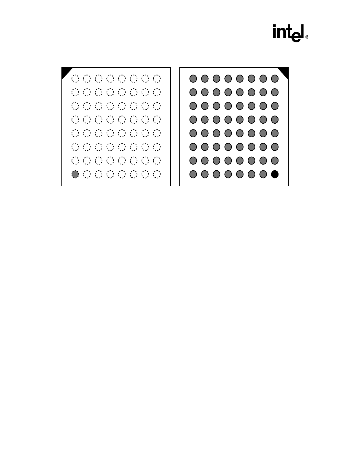
2.2 Ballout Diagram
The C3 device is available in 48-lead TSOP, 48-ball VF BGA, 48-ball µBGA, and Easy BGA
packages. (Refer to Figure1onpage9, Figure 3 on page 11,andFigure 4 on page 12,
respectively.)
8 Datasheet
Page 9
Figure 1. 48-Lead TSOP Package
Intel£Advanced+ Boot Block Flash Memory (C3)
64 M
32 M
16 M
A
15
A
14
A
13
A
12
A
11
A
10
A
9
A
8
A
21
A
20
WE#
RP#
V
PP
WP#
A
19
A
18
A
17
A
7
A
6
A
5
A
4
A
3
A
2
A
1
10
11
12
13
14
15
16
17
18
19
20
21
22
23
24
1
2
3
4
5
6
7
8
9
Advanced+ Boot Block
48-Lead TSOP
12 mm x 20 mm
TOP VIEW
48
47
46
45
44
43
42
41
40
39
38
37
36
35
34
33
32
31
30
29
28
27
26
25
A
16
V
CCQ
GND
DQ
DQ
DQ
DQ
DQ
DQ
DQ
DQ
V
CC
DQ
DQ
DQ
DQ
DQ
DQ
DQ
DQ
OE#
GND
CE#
A
0
15
7
14
6
13
5
12
4
11
3
10
2
9
1
8
0
NOTES:
1. For lower densities, upper address should be treated as NC. For example, a 16-Mbit device will have NC on
Pins 9 and 10.
Datasheet 9
Page 10
Intel£Advanced+ Boot Block Flash Memory (C3)
Figure 2. Mark for Pin-1 indicator on 48-Lead 8Mb, 16Mb and 32Mb TSOP
Current Mark:
New Mark:
Note: The topside marking on 8 Mb, 16 Mb, and 32 Mb Intel
£
Advanced and Advanced + Boot Block
48L TSOP products will convert to a white ink triangle as a Pin 1 indicator. Products without the
white triangle will continue to use a dimple as a Pin 1 indicator. There are no other changes in
package size, materials, functionality, customer handling, or manufacturability. Product will
continue to meet Intel stringent quality requirements. Products affected are Intel Ordering Codes
shown in Table 1 .
Table 1. 48-Lead TSOP
Extended 64 Mbit Extended 32 Mbit Extended 16 Mbit Extended 8 Mbit
TE28F640C3TC80
TE28F640C3BC80
TE28F320C3TD70
TE28F320C3BD70
TE28F320C3TC70
TE28F320C3BC70
TE28F320C3TC90
TE28F320C3BC90
TE28F320C3TA100
TE28F320C3BA100
TE28F320C3TA110
TE28F320C3BA110
TE28F160C3TD70
TE28F160C3BD70
TE28F160C3TC80
TE28F160C3BC80
TE28F160C3TA90
TE28F160C3BA90
TE28F160C3TA110
TE28F160C3BA110
TE28F800C3TA90
TE28F800C3BA90
TE28F800C3TA110
TE28F800C3BA110
10 Datasheet
Page 11
Intel£Advanced+ Boot Block Flash Memory (C3)
Figure 3. 48-Ball µBGA* and 48-Ball Very Fine Pitch BGA (VF BGA) Chip Size Package
(TopView,BallDown)
1,2,3
13254768
16M
A
B
A13
A14
A11
A10
A8
WE#
VPP
RP#
WP#
A18
A19
A17
A7
A5
A4
A2
32M64M
C
D
E
A15
A16
V
CCQ
A12
D14
D15
A9
D5
D6
A21
D11
D12
A20
D2
D3
A6
D8
D9
A3
CE#
D0
A1
A0
GND
F
GND D7 D13 D4 VCC D10 D1 OE#
NOTES:
1. Shaded connections indicate the upgrade address connections. Routing is not recommended in this area.
2. A19 denotes 16 Mbit; A20 denotes 32 Mbit; A21 denotes 64 Mbit.
3. Unused address balls are not populated.
Datasheet 11
Page 12
Intel£Advanced+ Boot Block Flash Memory (C3)
Figure 4. 64-Ball Easy BGA Package
1 2 3 4 5 6 7 8
A
A1A6A18VPPVCCGND A10A
B
A2A17A
C
A3A7WP# WE# DU A
D
A4A5DU
E
DQ
8DQ1DQ9DQ3DQ12DQ6
F
CE# DQ
G
A
0VSSQDQ2DQ4DQ13DQ15
H
(2)
A
22
NOTES:
1. A19 denotes 16 Mbit; A20 denotes 32 Mbit; A21 denotes 64 Mbit.
2. Unused address balls are not populated.
(1)
RP# DU A
19
DU DU DU A
0DQ10DQ11DQ5DQ14
OE# V
CCQVCCVSSQDQ7VCCQ
Top View
-BallSide
(1)
20
(1)
21
A11A
A12A
8A9
DU DU
DU DU
SSQ
V
1,2
A
15
14
13
16
DU
8 7 6 5 4 3 2 1
A
A
15A10
GND VCCVPPA18A6A
B
A14A11A
(1)
20
DU RP# A
(1)
19
C
A13A12A
(1)
DU WE# W P# A7A
21
D
A9A8DU
DU DU DU A5A
E
DU DU DQ
6DQ12DQ3DQ9DQ1DQ8
F
DU DU DQ14DQ5DQ11DQ
10
G
SSQ
V
A
16
D15D13DQ4DQ2V
H
DU V
CCQD7VSSQVCCVCCQ
Bottom View - Ball Side
A17A
DQ
0
SSQA0
OE# A
1
2
3
4
CE#
22
(2)
12 Datasheet
Page 13

Intel£Advanced+ Boot Block Flash Memory (C3)
2.3 Signal Descriptions
Tabl e 2 lists the active signals used and provides a brief description of each.
Table 2. Signal Descriptions
Symbol Type Name and Function
ADDRESS INPUTS for memory addresses. Address are internally latched during a program or erase
cycle.
A[MAX:0] INPUT
DQ[15:0]
CE# INPUT
OE# INPUT
RP# INPUT
WE# INPUT
WP# INPUT
VPP
VCC POWER
VCCQ POWER
GND POWER
DU -
NC -
INPUT/
OUTPUT
INPUT/
POWER
8 Mbit: AMAX= A18
16 Mbit: AMAX = A19
32 Mbit: AMAX = A20
64 Mbit: AMAX = A21
DATA INPUTS/OUTPUTS: Inputs data and commands during a write cycle; outputs data during read
cycles. Inputs commands to the Command User Interface when CE# and WE# are active. Data is
internally latched. The data pins float to tri-state when the chip is de-selected or the outputs are
disabled.
CHIP ENABLE: Active-low input. Activates the internal control logic, input buffers, decoders and sense
amplifiers. CE# is active low. CE# high de-selects the memory device and reduces power consumption
to standby levels.
OUTPUT ENABLE: Active-low input. Enables the device’s outputs through the data buffers during a
Read operation.
RESET/DEEP POWER-DOWN: Active-low input.
When RP# is at logic low, the device is in reset/deep power-down mode, which drives the outputs to
High-Z, resets the Write State Machine, and minimizes current levels (I
When RP# is at logic high, the device is in standard operation. When RP# transitions from logic-low to
logic-high, the device resets all blocks to locked and defaults to the read array mode.
WRITE ENABLE: Active-low input. WE# controls writes to the device. Address and data are latched on
therisingedgeoftheWE#pulse.
WRITE PROTECT: Active-low input.
When WP# is a logic low, the lock-down mechanism is enabled and blocks marked lock-down cannot
be unlocked through software.
When WP# is logic high, the lock-down mechanism is disabled and blocks previously locked-down are
now locked and can be unlocked and locked through software. After WP# goes low, any blocks
previously marked lock-down revert to the lock-down state.
See Section 5.0, “Security Modes” on page 27 for details on block locking.
PROGRAM/ERASE POWER SUPPLY: Operates as an input at logic levels to control complete device
protection. Supplies power for accelerated Program and Erase operations in 12 V
cannot be left floating.
Lower VPP
Set VPP = VCC for in-system Read, Program and Erase operations. In this configuration, VPP can
drop as low as 1.65 V to allow for resistor or diode drop from the system supply.
Apply VPP to 12 V
to VPP can only be done for a maximum of 1000 cycles on the main blocks and 2500 cycles on the
boot blocks. VPP may be connected to 12 V for a total of 80 hours maximum. See Section 5.6 for
details on VPP voltage configurations.
DEVICE CORE POWER SUPPLY: Supplies power for device operations.
OUTPUT POWER SUPPLY: Output-driven source voltage. This ball can be tied directly to V
operating within V
GROUND: For all internal circuitry. All ground inputs must be connected.
DON’T USE: Do not use this ball. This ball should not be connected to any power supplies, signals or
other balls, and must be left floating.
NO CONNECT: Pin must be left floating.
≤ VPPLK to protect all contents against Program and Erase commands.
± 5% for faster program and erase in a production environment. Applying 12 V ± 5%
range.
CC
CCD
).
± 5% range. This pin
CC
if
Datasheet 13
Page 14
Intel£Advanced+ Boot Block Flash Memory (C3)
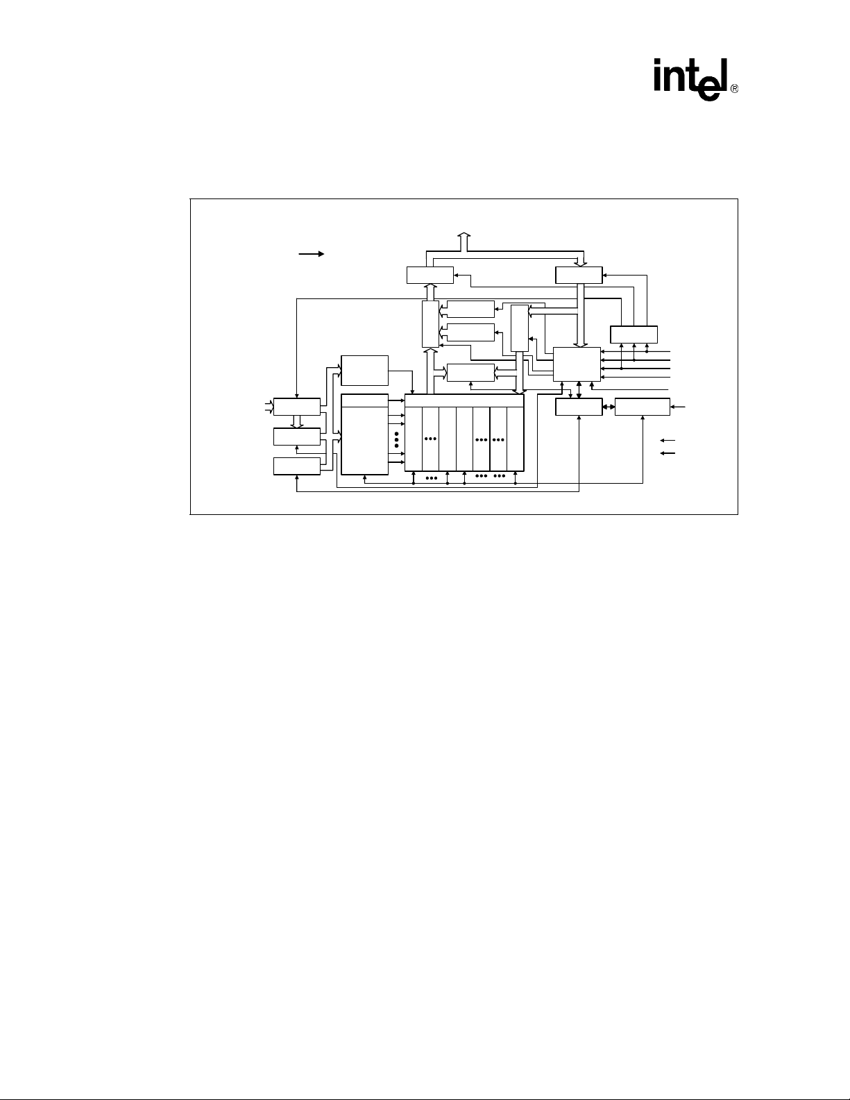
2.4 Block Diagram
V
CCQ
Power
Reduction
Control
A[MAX:MIN]
Input B uff er
Address
Latch
Address
Counter
Y-Decoder
X-Decoder
Output Buffer
Output
Multiplexer
Y-G ating/ Sensing
4-KWord
Paramet er B lock
DQ0-DQ
Comparat or
4-KWord
Paramet er B lock
Identifier
Register
Stat us
Register
Dat a
32- KWor d
Main Block
15
Input Buffer
Data
Re gist er
Command
User
Interface
Write State
Machine
32- KWor d
Main Block
I/O Logic
Program /Eras e
Voltage Switch
CE#
WE#
OE#
RP#
WP#
V
GND
V
PP
CC
14 Datasheet
Page 15
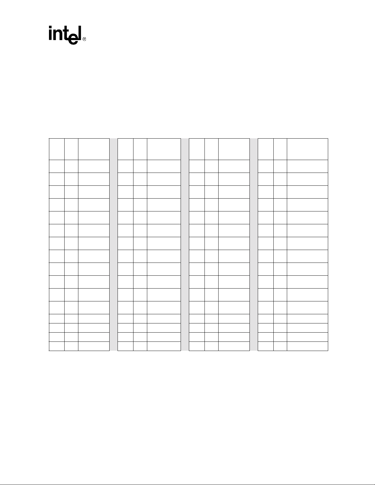
2.5 Memory Map
The C3 device is asymmetrically blocked, which enables system code and data integration within a
single flash device. The bulk of the array is divided into 32 Kword main blocks that can store code
or data, and 4 Kword boot blocks to facilitate storage of boot code or for frequently changing small
parameters. See Table 3, “Top Boot Memory Map” on page 15 and Table 4, “Bottom Boot Memory
Map” on page 16 for details.
Table 3. Top Boot Memory Map
Size
Blk
(KW)
422
421
420
419
418
417
4 16 79000-79FFF
4 15 78000-78FFF
32 14 70000-77FFF
32 13 68000-6FFFF
32 12 60000-67FFF
32 11 58000-5FFFF
... ... ...
32 2 10000-17FFF
32 1 8000-0FFFF
32 0 0000-07FFF
8-Mbit
Memory
Addressing
(HEX)
7F000-
7FFFF
7E000-
7EFFF
7D0007DFFF
7C0007CFFF
7B000-
7BFFF
7A000-
7AFFF
Size
(KW)
4 38 FF000-FFFFF 470
4 37 FE000-FEFFF 469
4 36 FD000-FDFFF 468
4 35 FC000-FCFFF 467
4 34 FB000-FBFFF 466
4 33 FA000-FAFFF 465
4 32 F9000-F9FFF 464
4 31 F8000-F8FFF 463
32 30 F0000-F7FFF 32 62
32 29 E8000-EFFFF 32 61
32 28 E0000-E7FFF 32 60
32 27 D8000-DFFFF 32 59
... ... ... ... ... ... ... ... ...
32 2 10000-17FFF 32 2 10000-17FFF 32 2 10000-17FFF
32 1 08000-0FFFF 32 1 08000-0FFFF 32 1 08000-0FFFF
32 0 00000-07FFF 32 0 00000-07FFF 32 0 00000-07FFF
Blk
16-Mbit
Memory
Addressing
(HEX)
Intel£Advanced+ Boot Block Flash Memory (C3)
Size
(KW)
Blk
32-Mbit
Memory
Addressing
(HEX)
1FF000-
1FFFFF
1FE000-
1FEFFF
1FD000-
1FDFFF
1FC000-
1FCFFF
1FB000-
1FBFFF
1FA000-
1FAFFF
1F90001F9FFF
1F80001F8FFF
1F00001F7FFF
1E8000-
1EFFFF
1E0000-
1E7FFF
1D8000-
1DFFFF
Size
(KW)
4 134 3FF000-3FFFFF
4 133 3FE000-3FEFFF
4 132 3FD000-3FDFFF
4 131 3FC000-3FCFFF
4 130 3FB000-3FBFFF
4 129 3FA000-3FAFFF
4 128 3F9000-3F9FFF
4 127 3F8000-3F8FFF
32 126 3F0000-3F7FFF
32 125 3E8000-3EFFFF
32 124 3E0000-3E7FFF
32 123 3D8000-3DFFFF
Blk
64-Mbit Memory
Addressing
(HEX)
Datasheet 15
Page 16
Intel£Advanced+ Boot Block Flash Memory (C3)
Table 4. Bottom Boot Memory Map
Size
Blk
(KW)
32 22 78000-7FFFF
32 21 70000-77FFF
32 20 68000-6FFFF
32 19 60000-67FFF
... ... ...
32 10 18000-1FFFF
32 9 10000-17FFF
32 8 08000-0FFFF
4 7 07000-07FFF
4 6 06000-06FFF
4 5 05000-05FFF
4 4 04000-04FFF
4 3 03000-03FFF
4 2 02000-02FFF
4 1 01000-01FFF
4 0 00000-00FFF
8-Mbit
Memory
Addressing
(HEX)
Size
Blk
(KW)
32 38 F8000-FFFFF 32 70 1F8000-1FFFFF 32 134 3F8000-3FFFFF
32 37 F0000-F7FFF 32 69 1F0000-1F7FFF 32 133 3F0000-3F7FFF
32 36 E8000-EFFFF 32 68 1E8000-1EFFFF 32 132 3E8000-3EFFFF
32 35 E0000-E7FFF 32 67 1E0000-1E7FFF 32 131 3E0000-3E7FFF
... ... ... ... ... ... . ... ...
32 10 18000-1FFFF 32 10 18000-1FFFF 32 10 18000-1FFFF
32 9 10000-17FFF 32 9 10000-17FFF 32 9 10000-17FFF
32 8 08000-0FFFF 32 8 08000-0FFFF 32 8 08000-0FFFF
4 7 07000-07FFF 4 7 07000-07FFF 4 7 07000-07FFF
4 6 06000-06FFF 4 6 06000-06FFF 4 6 06000-06FFF
4 5 05000-05FFF 4 5 05000-05FFF 4 5 05000-05FFF
4 4 04000-04FFF 4 4 04000-04FFF 4 4 04000-04FFF
4 3 03000-03FFF 4 3 03000-03FFF 4 3 03000-03FFF
4 2 02000-02FFF 4 2 02000-02FFF 4 2 02000-02FFF
4 1 01000-01FFF 4 1 01000-01FFF 4 1 01000-01FFF
4 0 00000-00FFF 4 0 00000-00FFF 4 0 00000-00FFF
16-Mbit
Memory
Addressing
(HEX)
Size
(KW)
Blk
32-Mbit
Memory
Addressing
(HEX)
Size
(KW)
Blk
64-Mbit Memory
Addressing
(HEX)
16 Datasheet
Page 17

3.0 Device Operations
The C3 device uses a CUI and automated algorithms to simplify Program and Erase operations.
The CUI allows for 100% CMOS
programming.
The internal WSM completely automates Program and Erase operations while the CUI signals the
start of an operation and the status register reports device status. The CUI handles the WE#
interface to the data and address latches, as well as system status requests during WSM operation.
3.1 Bus Operations
The C3 device performs read, program, and erase operations in-system via the local CPU or
microcontroller. Four control pins (CE#, OE#, WE#, and RP#) manage the data flow in and out of
the flash device. Table 5 on page 17 summarizes these bus operations.
Table 5. Bus Operations
Intel£Advanced+ Boot Block Flash Memory (C3)
-level control inputs and fixed power supplies during erasure and
3.1.1 Read
When performing a read cycle, CE# and OE# must be asserted; WE# and RP# must be deasserted.
CE# is the device selection control; when active low, it enables the flash memory device. OE# is
the data output control; when low, data is output on DQ[15:0]. See Figure 8, “Read Operation
Wav ef orm” on page 42.
3.1.2 Write
A write cycle occurs when both CE# and WE# are low; RP# and OE# are high. Commands are
issued to the Command User Interface (CUI). The CUI does not occupy an addressable memory
location. Address and data are latched on the rising edge of the WE# or CE# pulse, whichever
occurs first. See Figure 9, “Write Operations Waveform” on page 47.
Mode RP# CE# OE# WE# DQ[15:0]
Read V
Write V
Output Disable V
Standby V
Reset V
NOTE: X = Don’t Care (V
IL
or VIH)
IH
IH
IH
IH
IL
V
IL
V
IL
V
IL
V
IH
XXXHigh-Z
V
IL
V
IH
V
IH
X X High-Z
V
IH
V
IL
V
IH
D
OUT
D
High-Z
IN
3.1.3 Output Disable
With OE# at a logic-high level (VIH), the device outputs are disabled. DQ[15:0] are placed in a
-impedance state.
high
Datasheet 17
Page 18

Intel£Advanced+ Boot Block Flash Memory (C3)
3.1.4 Standby
Deselecting the device by bringing CE# to a logic-high level (VIH) places the device in standby
mode, which substantially reduces device power consumption without any latency for subsequent
read accesses. In standby, outputs are placed in a high-impedance state independent of OE#. If
deselected during a Program or Erase operation, the device continues to consume active power
until the Program or Erase operation is complete.
3.1.5 Reset
From read mode, RP# at VILfor time t
impedance state, and turns off all internal circuits. After return from reset, a time t
until the initial read-access outputs are valid. A delay (t
reset before a write cycle can be initiated. After this wake
deselects the memory, places output drivers in a high-
PLPH
PHQV
PHWL
or t
) is required after return from
PHEL
-up interval, normal operation is restored.
is required
The CUI resets to read-array mode, the status register is set to 0x80, and all blocks are locked. See
Figure 10, “Reset Operations Waveforms” on page 48.
If RP# is taken low for time t
during a Program or Erase operation, the operation will be
PLPH
aborted and the memory contents at the aborted location (for a program) or block (for an erase) are
no longer valid, since the data may be partially erased or written. The abort process goes through
the following sequence:
1. When RP# goes low, the device shuts down the operation in progress, a process which takes time
to complete.
t
PLRH
2. After time t
enter reset mode (if RP# is deasserted after t
, the part will either reset to read-array mode (if RP# is asserted during t
PLRH
). See Figure 10, “Reset Operations Waveforms”
PLRH
PLRH
)or
on page 48.
In both cases, after returning from an aborted operation, the relevant time t
PHQV
or t
PHWL/tPHEL
must be observed before a Read or Write operation is initiated, as discussed in the previous
paragraph. However, in this case, these delays are referenced to the end of t
rather than when
PLRH
RP# goes high.
As with any automated device, it is important to assert RP# during a system reset. When the system
comes out of reset, the processor expects to read from the flash memory. Automated flash
memories provide status information when read during program or Block-Erase operations. If a
CPU reset occurs with no flash memory reset, proper CPU initialization may not occur because the
flash memory may be providing status information instead of array data. Intel
®
Flash memories
allow proper CPU initialization following a system reset through the use of the RP# input. In this
application, RP# is controlled by the same RESET# signal that resets the system CPU.
18 Datasheet
Page 19

4.0 Modes of Operation
4.1 Read Mode
The flash memory has four read modes (read array, read identifier, read status, and CFI query), and
two write modes (program and erase). Three additional modes (erase suspend to program, erase
suspend to read, and program suspend to read) are available only during suspended operations.
Table 7, “Command Bus Operations” on page 24 and Table 8, “Command Codes and
Descriptions”onpage25summarize the commands used to reach these modes. Appendix A,
“Write State Machine States” on page 50 is a comprehensive chart showing the state transitions.
4.1.1 Read Array
When RP# transitions from VIL(reset) to VIH, the device defaults to read-array mode and will
respond to the read-control inputs (CE#, address inputs, and OE#) without any additional CUI
commands.
When the device is in read array mode, four control signals control data output.
• WE# must be logic high (V
• CE# must be logic low (V
• OE# must be logic low (V
• RP#mustbelogichigh(V
)
IH
)
IL
)
IL
)
IH
Intel£Advanced+ Boot Block Flash Memory (C3)
In addition, the address of the desired location must be applied to the address pins. If the device is
not in read-array mode, as would be the case after a Program or Erase operation, the Read Array
command (0xFF) must be issued to the CUI before array reads can occur.
4.1.2 Read Identifier
The read-identifier mode outputs three types of information: the manufacturer/device identifier, the
block locking status, and the protection register. The device is switched to this mode by issuing the
Read Identifier command (0x90). Once in this mode, read cycles from addresses shown in Table 6
retrieve the specified information. To return to read-array mode, issue the Read Array command
(0xFF).
Datasheet 19
Page 20

Intel£Advanced+ Boot Block Flash Memory (C3)
Table 6. Device Identification Codes
Item
Manufacturer ID Block 0x00 0x0089
Device ID Block 0x01
Block Lock Status
Block Lock-Down Status
Protection Register Lock Status Block 0x80 Lock Data
Protection Register Block
NOTES:
1. The address is constructed from a base address plus an offset. For example, to read the Block Lock Status
for block number 38 in a bottom boot device, set the address to 0x0F8000 plus the
0x0F8002. Then examine DQ0 of the data to determine if the block is locked.
2. See Section 5.2, “Reading Block-Lock Status” on page 28 for valid lock status.
2
2
Address
Base Offset
Block 0x02
Block 0x02
1
0x81 -
0x88
Data Description
0x88C0 8-Mbit Top Boot Device
0x88C1 8-Mbit Bottom Boot Device
0x88C2 16-Mbit Top Boot Device
0x88C3 16-Mbit Bottom Boot Device
0x88C4 32-Mbit Top Boot Device
0x88C5 32-Mbit Bottom Boot Device
0x88CC 64-Mbit Top Boot Device
0x88CD 64-Mbit Bottom Boot Device
DQ0 = 0b0 Block is unlocked
DQ0 = 0b1 Block is locked
DQ1 = 0b0 Block is not locked-down
DQ1 = 0b1 Block is locked down
Register Data
Multiple reads required to read
the entire 128-bit Protection
Register.
offset (0x02), i.e.
4.1.3 CFI Query
The CFI query mode outputs Common Flash Interface (CFI) data after issuing the Read Query
Command (0x98). The CFI data structure contains information such as block size, density,
command set, and electrical specifications. Once in this mode, read cycles from addresses shown in
Appendix C, “Common Flash Interface,” retrieve the specified information. To return to read-array
mode, issue the Read Array command (0xFF).
4.1.4 Read Status Register
The status register indicates the status of device operations, and the success/failure of that
operation. The Read Status Register (0x70) command causes subsequent reads to output data from
the status register until another command is issued. To return to reading from the array, issue a
Read Array (0xFF) command.
The status-register bits are output on DQ[7:0]. The upper byte, DQ[15:8], outputs 0x00 when a
Read Status Register command is issued.
20 Datasheet
Page 21

The contents of the status register are latched on the falling edge of OE# or CE# (whichever occurs
last) which prevents possible bus errors that might occur if Status Register contents change while
being read. CE# or OE# must be toggled with each subsequent status read, or the Status Register
will not indicate completion of a Program or Erase operation.
When the WSM is active, SR[7] will indicate the status of the WSM; the remaining bits in the
status register indicate whether the WSM was successful in performing the preferred operation (see
Table 9, “Status Register Bit Definition” on page 26).
4.1.4.1 Clear Status Register
The WSM can set Status Register bits 1 through 7 and can clear bits 2, 6, and 7; but, the WSM
cannot clear Status Register bits 1, 3, 4 or 5. Because bits 1, 3, 4, and 5 indicate various error
conditions, these bits can be cleared only through the Clear Status Register (0x50) command. By
allowing the system software to control the resetting of these bits, several operations may be
performed (such as cumulatively programming several addresses or erasing multiple blocks in
sequence) before reading the status register to determine if an error occurred during that series.
Clear the status register before beginning another command or sequence. The Read Array
command must be issued before data can be read from the memory array. Resetting the device also
clears the Status Register.
Intel£Advanced+ Boot Block Flash Memory (C3)
4.2 Program Mode
Programming is executed using a two-write cycle sequence. The Program Setup command (0x40)
is issued to the CUI followed by a second write which specifies the address and data to be
programmed. The WSM will execute a sequence of internally timed events to program preferred
bits of the addressed location, then verify the bits are sufficiently programmed. Programming the
memory results in specific bits within an address location being changed to a “0.” If users attempt
to program “1”s, the memory cell contents do not change and no error occurs.
The Status Register indicates programming status. While the program sequence executes, status bit
7 is “0.” The status register can be polled by toggling either CE# or OE#. While programming, the
only valid commands are Read Status Register, Program Suspend, and Program Resume.
When programming is complete, the program-status bits should be checked. If the programming
operation was unsuccessful, bit SR[4] of the Status Register is set to indicate a program failure. If
SR[3] is set, then V
command. If SR[1] is set, a program operation was attempted on a locked block and the operation
was aborted.
The status register should be cleared before attempting the next operation. Any CUI instruction can
follow after programming is completed; however, to prevent inadvertent status-register reads, be
sure to reset the CUI to read-array mode.
4.2.1 12-Volt Production Programming
When VPPis between 1.65 V and 3.6 V, all program and erase current is drawn through the VCC
pin. Note that if V
1.65 V to perform in-system flash modifications. When V
the device draws program and erase current directly from the VPP pin. This eliminates the need for
an external switching transistor to control V
flash power supplies can be configured for various usage models.
was not within acceptable limits, and the WSM did not execute the program
PP
is driven by a logic signal, VIHmin = 1.65 V. That is, VPPmust remain above
PP
PP
is connected to a 12 V power supply,
PP
. Figure 7 on page 31 shows examples of how the
Datasheet 21
Page 22

Intel£Advanced+ Boot Block Flash Memory (C3)
The 12 V VPPmode enhances programming performance during the short period of time typically
found in manufacturing processes; however, it is not intended for extended use. 12 V may be
applied to VPP during Program and Erase operations for a maximum of 1000 cycles on the main
blocks and 2500 cycles on the parameter blocks. VPP may be connected to 12 V for a total of 80
hours maximum. Stressing the device beyond these limits may cause permanent damage.
4.2.2 Suspending and Resuming Program
The Program Suspend command halts an in-progress program operation so that data can be read
from other locations of memory. Once the programming process starts, issuing the Program
Suspend command to the CUI requests that the WSM suspend the program sequence at
predetermined points in the program algorithm. The device continues to output status-register data
after the Program Suspend command is issued. Polling status-register bits SR[7] and SR[2] will
determine when the program operation has been suspended (both will be set to “1”). t
t
A Read-Array command can now be issued to the CUI to read data from blocks other than that
which is suspended. The only other valid commands while program is suspended are Read Status
Register, Read Identifier, CFI Query, and Program Resume.
After the Program Resume command is issued to the flash memory, the WSM will continue with
the programming process and status register bits SR[2] and SR[7] will automatically be cleared.
The device automatically outputs status register data when read (see Figure 14, “Program Suspend
/ResumeFlowchart”onpage53) after the Program Resume command is issued. V
atthesameV
V
specify the program-suspend latency.
EHRH1
level used for program while in program-suspend mode. RP# must also remain at
PP
IH
.
WHRH1
must remain
PP
/
4.3 Erase Mode
To erase a block, issue the Erase Set-up and Erase Confirm commands to the CUI, along with an
address identifying the block to be erased. This address is latched internally when the Erase
Confirm command is issued. Block erasure results in all bits within the block being set to “1.” Only
one block can be erased at a time. The WSM will execute a sequence of internally timed events to
program all bits within the block to “0,” erase all bits within the block to “1,” then verify that all
bits within the block are sufficiently erased. While the erase executes, status bit 7 is a “0.”
When the status register indicates that erasure is complete, check the erase-status bit to verify that
the Erase operation was successful. If the Erase operation was unsuccessful, SR[5] of the status
register will be set to a “1,” indicating an erase failure. If V
the Erase Confirm command was issued, the WSM will not execute the erase sequence; instead,
SR[5] of the status register is set to indicate an erase error, and SR[3] is set to a “1” to identify that
supply voltage was not within acceptable limits.
V
PP
After an Erase operation, clear the status register (0x50) before attempting the next operation. Any
CUI instruction can follow after erasure is completed; however, to prevent inadvertent statusregister reads, it is advisable to place the flash in read-array mode after the erase is complete.
was not within acceptable limits after
PP
22 Datasheet
Page 23

Intel£Advanced+ Boot Block Flash Memory (C3)
4.3.1 Suspending and Resuming Erase
Since an Erase operation requires on the order of seconds to complete, an Erase Suspend command
is provided to allow erase
another block in memory. Once the erase sequence is started, issuing the Erase Suspend command
to the CUI suspends the erase sequence at a predetermined point in the erase algorithm. The status
register will indicate if/when the Erase operation has been suspended. Erase-suspend latency is
specified by t
WHRH2/tEHRH2
A Read Array or Program command can now be issued to the CUI to read/program data from/to
blocks other than that which is suspended. This nested Program command can subsequently be
suspended to read yet another location. The only valid commands while Erase is suspended are
Read Status Register, Read Identifier, CFI Query, Program Setup, Program Resume, Erase
Resume, Lock Block, Unlock Block, and Lock-Down Block. During erase-suspend mode, the chip
can be placed in a pseudo
consumption.
-sequence interruption in order to read data from—or program data to—
.
-standbymodebytakingCE#toV
, which reduces active current
IH
Erase Resume continues the erase sequence when CE# = V
. Similar to the end of a standard
IL
Erase operation, the status register should be read and cleared before the next instruction is issued.
Datasheet 23
Page 24

Intel£Advanced+ Boot Block Flash Memory (C3)
Table 7. Command Bus Operations
Command Notes
Read Array 1,3 Write X 0xFF
Read Identifier 1,3 Write X 0x90 Read IA ID
CFI Query 1,3 Write X 0x98 Read QA QD
Read Status Register 1,3 Write X 0x70 Read X SRD
Clear Status Register 1,3 Write X 0x50
Program 2,3 Write X
Block Erase/Confirm 1,3 Write X 0x20 Write BA D0H
Program/Erase Suspend 1,3 Write X 0xB0
Program/Erase Resume 1,3 Write X 0xD0
Lock Block 1,3 Write X 0x60 Write BA 0x01
Unlock Block 1,3 Write X 0x60 Write BA 0xD0
Lock-Down Block 1,3 Write X 0x60 Write BA 0x2F
Protection Program 1,3 Write X 0xC0 Write PA PD
X = "Don’t Care" PA = Prog Addr BA = Block Addr IA = Identifier Addr. QA = Query Addr.
SRD = Status Reg.
Data
NOTES:
1. Following the Read Identifier or CFI Query commands, read operations output device identification data or
CFI query information, respectively. See Section 4.1.2 and Section 4.1.3.
2. Either 0x40 or 0x10 command is valid, but the Intel standard is 0x40.
3. When writing commands, the upper data bus [DQ8-DQ15] should be either V
draw.
PD = Prog Data ID = Identifier Data QD = Query Data
First Bus Cycle Second Bus Cycle
Oper Addr Data Oper Addr Data
0x40/
0x10
Write PA PD
or VIH, to minimize current
IL
Bus operations are defined in Table 5, “Bus Operations” on page 17.
24 Datasheet
Page 25

Table 8. Command Codes and Descriptions
Intel£Advanced+ Boot Block Flash Memory (C3)
Code
(HEX)
FF Read Array
40 Program Set-Up
20 Erase Set-Up
D0
B0
70
50
90
60
01 Lock-Block
2F Lock-Down
98
C0
Device Mode Command Description
Erase Confirm
Program/Erase
Resume
Unlock Block
Program Suspend
Erase Suspend
Read Status
Register
Clear Status
Register
Read
Identifier
Block Lock, Block
Unlock, Block
Lock-Down Set-
Up
CFI
Query
Protection
Program
Set-Up
This command places the device in read-array mode, which outputs array data on the data
pins.
This is a two
second cycle latches addresses and data information and initiates the WSM to execute the
Program algorithm. The flash outputs status-register data when CE# or OE# is toggled. A Read
Array command is required after programming to read array data. See Section 4.2, “Program
Mode” on page 21.
This is a two
command is not an Erase Confirm command, then the CUI will (a) set both SR.4 and SR.5 of
the status register to a “1,” (b) place the device into the read-status-register mode, and (c) wait
for another command. See Section 4.3, “Erase Mode” on page 22.
If the previous command was an Erase Set-Up command, then the CUI will close the address
and data latches and begin erasing the block indicated on the address pins. During program/
erase, the device will respond only to the Read Status Register, Program Suspend and Erase
Suspend commands, and will output status-register data when CE# or OE# is toggled.
If a Program or Erase operation was previously suspended, this command will resume that
operation.
If the previous command was Block Unlock Set-Up, the CUI will latch the address and unlock
the block indicated on the address pins. If the block had been previously set to Lock-Down, this
operation will have no effect. (See Section 5.1)
Issuing this command will begin to suspend the currently executing Program/Erase operation.
The status register will indicate when the operation has been successfully suspended by
setting either the program-suspend SR[2] or erase-suspend SR[6] and the WSM status bit
SR[7] to a “1” (ready). The WSM will continue to idle in the SUSPEND state, regardless of the
state of all input-control pins except RP#, which will immediately shut down the WSM and the
remainderofthechipifRP#isdriventoV
This command places the device into read-status-register mode. Reading the device will
output the contents of the status register, regardless of the address presented to the device.
The device automatically enters this mode after a Program or Erase operation has been
initiated. See Section 4.1.4, “Read Status Register” on page 20.
The WSM can set the block-lock status SR[1], V
erase-status SR[5] bits in the status register to “1,” but it cannot clear them to “0.” Issuing this
command clears those bits to “0.”
Puts the device into the read-identifier mode so that reading the device will output the
manufacturer/device codes or block-lock status. See Section 4.1.2, “Read Identifier” on
page 19.
Prepares the CUI for block-locking changes. If the next command is not Block Unlock, Block
Lock, or Block Lock-Down, then the CUI will set both the program and erase-status-register
bits to indicate a command-sequence error. See Section 5.0, “Security Modes” on page 27.
If the previous command was Lock Set-Up, the CUI will latch the address and lock the block
indicated on the address pins. (See Section 5.1)
If the previous command was a Lock-Down Set-Up command, the CUI will latch the address
and lock-down the block indicated on the address pins. (See Section 5.1)
Puts the device into the CFI-Query mode so that reading the device will output Common Flash
Interface information. See Section 4.1.3 and Appendix C, “Common Flash Interface”.
This is a two-cycle command. The first cycle prepares the CUI for a program operation to the
protection register. The second cycle latches addresses and data information and initiates the
WSM to execute the Protection Program algorithm to the protection register. The flash outputs
status-register data when CE# or OE# is toggled. A Read Array command is required after
programming to read array data. See Section 5.5.
-cycle command. The first cycle prepares the CUI for a program operation. The
-cycle command. Prepares the CUI for the Erase Confirm command. If the next
. See Sections 3.2.5.1 and 3.2.6.1.
IL
Status SR[3], program status SR[4], and
PP
Datasheet 25
Page 26

Intel£Advanced+ Boot Block Flash Memory (C3)
Table 8. Command Codes and Descriptions
Code
(HEX)
Device Mode Command Description
10 Alt. Prog Set-Up Operates the same as Program Set-up command. (See 0x40/Program Set-Up)
00
NOTE: See Appendix A, “Write State Machine States” for mode transition information.
Invalid/
Reserved
Unassigned commands should not be used. Intel reserves the right to redefine these codes for
future functions.
Table 9. Status Register Bit Definition
WSMS ESS ES PS VPPS PSS BLS R
76543210
NOTES:
SR[7] WRITE STATE MACHINE STATUS (WSMS)
1 = Ready
0=Busy
SR[6] = ERASE
-SUSPEND STATUS (ESS)
1 = Erase Suspended
0=EraseInProgress/Completed
SR[5] = ERASE STATUS (ES)
1=ErrorInBlockErase
0 = Successful Block Erase
SR[4] = PROGRAM STATUS (PS)
1 = Error in Programming
0 = Successful Programming
SR[3] = V
1=V
0=V
STATUS (VPPS)
PP
Low Detect, Operation Abort
PP
OK
PP
SR[2] = PROGRAM SUSPEND STATUS (PSS)
1 = Program Suspended
0 = Program in Progress/Completed
SR[1] = BLOCK LOCK STATUS
1=Prog/Eraseattemptedonalockedblock;Operation
aborted.
0=Nooperationtolockedblocks
SR[0] = RESERVED FOR FUTURE ENHANCEMENTS (R)
NOTE: A Command-Sequence Error is indicated when SR[4], SR[5], and SR[7] are set.
Check Write State Machine bit first to determine Word Program
or Block Erase completion, before checking program or erasestatus bits.
When Erase Suspend is issued, WSM halts execution and sets
both WSMS and ESS bits to “1.” ESS bit remains set to “1” until
an Erase Resume command is issued.
When this bit is set to “1,” WSM has applied the max. number
of erase pulses to the block and is still unable to verify
successful block erasure.
When this bit is set to “1,” WSM has attempted but failed to
program a word/byte.
The V
V
Program or Erase command sequences have been entered,
and informs the system if V
V
WSM. The V
feedback between V
status bit does not provide continuous indication of
PP
level. The WSM interrogates VPPlevel only after the
PP
has not been switched on. The
PPLK
PP
and V
PP1
Min.
is also checked before the operation is verified by the
PP
status bit is not guaranteed to report accurate
PP
When Program Suspend is issued, WSM halts execution and
sets both WSMS and PSS bits to “1.” PSS bit remains set to “1”
until a Program Resume command is issued.
If a Program or Erase operation is attempted to one of the
locked blocks, this bit is set by the WSM. The operation
specifiedisabortedandthedeviceisreturnedtoreadstatus
mode.
This bit is reserved for future use and should be masked out
when polling the status register.
26 Datasheet
Page 27

5.0 Security Modes
5.1 Flexible Block Locking
The C3 device offers an instant, individual block-locking scheme that allows any block to be
locked or unlocked with no latency, enabling instant code and data protection.
This locking scheme offers two levels of protection. The first level allows software-only control of
block locking (useful for data blocks that change frequently), while the second level requires
hardware interaction before locking can be changed (useful for code blocks that change
infrequently).
The following sections will discuss the operation of the locking system. The term “state [abc]” will
be used to specify locking states; e.g., “state [001],” where a = value of WP#, b = bit D1 of the
Block Lock status register, and c = bit D0 of the Block Lock status register. Figure 5, “Block
Locking State Diagram” on page 27 displays all of the possible locking states.
Figure 5. Block Locking State Diagram
Intel£Advanced+ Boot Block Flash Memory (C3)
Power-U p/Reset
Not es: 1. [ a,b,c ] represents [WP#, D 1, D0]. X = Don’t Care.
2. D 1 indic ates block Lock-down s tatus . D 1 = ‘0’, Lock-dow n has not been issued t o
this bloc k. D1 = ‘1’, Lock-down has been is sued t o this block .
3. D 0 indic ates block lock s tatus. D 0 = ‘0’, block is unloc ked. D0 = ‘1’, bloc k is loc k ed.
4. Loc ked-down = Hardware + Sof tware lock ed.
5. [ 011] st at es s hould be t rac ked by sys tem s oftware to determ ine difference
betw een H ardware Locked and Loc ked-Down s tates .
Lo cked
[X01]
Unlo cked
[X00]
Software Block Lock (0x60/0x01) or Software Block Unlock (0x60/0xD0)
Software Block Lock-Down (0x60/0x2F)
WP# hardware control
Lo cked-
Down
Software
4,5
[011]
WP#HardwareControl
Lo cked
[111] [ 110]
Hardware
Lo cked
[011]
Unlo cked
5
Datasheet 27
Page 28

Intel£Advanced+ Boot Block Flash Memory (C3)
5.1.1 Locking Operation
The locking status of each block can be set to Locked, Unlocked, or Lock-Down, each of which
will be described in the following sections. See Figure 5, “Block Locking State Diagram” on
page 27 and Figure 17, “Locking Operations Flowchart” on page 56.
The following concisely summarizes the locking functionality.
5.1.1.1 Locked State
The default state of all blocks upon power-up or reset is locked (states [001] or [101]). Locked
blocks are fully protected from alteration. Any Program or Erase operations attempted on a locked
block will return an error on bit SR[1] of the Status Register. The state of a locked block can be
changed to Unlocked or Lock Down using the appropriate software commands. An Unlocked
block can be locked by writing the Lock command sequence, 0x60 followed by 0x01.
5.1.1.2 Unlocked State
Unlocked blocks (states [000], [100], [110]) can be programmed or erased. All unlocked blocks
return to the Locked state when the device is reset or powered down. The status of an unlocked
block can be changed to Locked or Locked Down using the appropriate software commands. A
Locked block can be unlocked by writing the Unlock command sequence, 0x60 followed by 0xD0.
5.1.1.3 Lock-Down State
Blocks that are Locked-Down (state [011]) are protected from Program and Erase operations (just
like Locked blocks), but their protection status cannot be changed using software commands alone.
A Locked or Unlocked block can be Locked Down by writing the Lock-Down command sequence,
0x60 followed by 0x2F. Locked-Down blocks revert to the Locked state when the device is reset or
powered down.
The Lock-Down function depends on the WP# input pin. When WP# = 0, blocks in Lock Down
[011] are protected from program, erase, and lock status changes. When WP# = 1, the Lock-Down
function is disabled ([111]) and Locked-Down blocks can be individually unlocked by software
command to the [110] state, where they can be erased and programmed. These blocks can then be
relocked [111] and unlocked [110] as required while WP# remains high. When WP# goes low,
blocks that were previously Locked Down return to the Lock-Down state [011], regardless of any
changes made while WP# was high. Device reset or power-down resets all blocks, including those
in Lock-Down, to Locked state.
5.2 Reading Block-Lock Status
The Lock status of each block can be read in read-identifier mode of the device by issuing the readidentifier command (0x90). Subsequent reads at Block Address + 0x00002 will output the Lock
status of that block. The Lock status is represented by DQ0 and DQ1. DQ0 indicates the Block
Lock/Unlock status and is set by the Lock command and cleared by the Unlock command. It is also
automatically set when entering Lock Down. DQ1 indicates Lock-Down status, and is set by the
Lock-Down command. It cannot be cleared by software—only by device reset or power-down. See
Table 6, “Device Identification Codes” on page 20 for block-status information.
28 Datasheet
Page 29

Intel£Advanced+ Boot Block Flash Memory (C3)
5.3 Locking Operations during Erase Suspend
Changes to block-lock status can be performed during an erase-suspend by using the standard
locking command sequences to Unlock, Lock, or Lock Down a block. This is useful in the case
when another block needs to be updated while an Erase operation is in progress.
To change block locking during an Erase operation, first issue the Erase Suspend command (0xB0),
then check the status register until it indicates that the Erase operation has been suspended. Next,
write the preferred Lock command sequence to a block and the Lock status will be changed. After
completing any preferred Lock, Read, or Program operations, resume the Erase operation with the
Erase Resume command (0xD0).
If a block is Locked or Locked Down during a Suspended Erase of the same block, the locking
status bits will be changed immediately. But when the Erase is resumed, the Erase operation will
complete.
Locking operations cannot be performed during a Program Suspend. Refer to Appendix A, “Write
State Machine States” on page 50 for detailed information on which commands are valid during
Erase Suspend.
5.4 Status Register Error Checking
Using nested-locking or program-command sequences during Erase Suspend can introduce
ambiguity into status register results.
Since locking changes are performed using a two-cycle command sequence, e.g., 0x60 followed by
0x01 to lock a block, following the Block Lock, Block Unlock, or Block Lock-Down Setup
command (0x60) with an invalid command will produce a Lock-Command error (SR[4] and SR[5]
will be set to 1) in the Status Register. If a Lock-Command error occurs during an Erase Suspend,
SR[4] and SR[5] will be set to 1 and will remain at 1 after the Erase is resumed. When Erase is
complete, any possible error during the Erase cannot be detected via the status register because of
the previous Lock-Command error.
A similar situation happens if an error occurs during a Program-Operation error nested within an
Erase Suspend.
5.5 128-Bit Protection Register
The C3 device architecture includes a 128-bit protection register than can be used to increase the
security of a system design. For example, the number contained in the protection register can be
used to “match” the flash component with other system components, such as the CPU or ASIC,
preventing device substitution. The Intel application note,
Boot Block Flash Memory Architecture,
The 128 bits of the protection register are divided into two 64-bit segments. One of the segments is
programmed at the Intel factory with a unique 64-bit number, which is unchangeable. The other
segment is left blank for customer designs to program, as preferred. Once the customer segment is
programmed, it can be locked to prevent further programming.
contains additional application information.
AP-657 Designing with the Advanced+
Datasheet 29
Page 30

Intel£Advanced+ Boot Block Flash Memory (C3)
5.5.1 Reading the Protection Register
The protection register is read in the read-identifier mode. The device is switched to this mode by
issuing the Read Identifier command (0x90). Once in this mode, read cycles from addresses shown
in Figure 6, “Protection Register Mapping” retrieve the specified information. To return to readarray mode, issue the Read Array command (0xFF).
5.5.2 Programming the Protection Register
The protection register bits are programmed using the two-cycle Protection Program command.
The 64-bit number is programmed 16 bits at a time. First, issue the Protection Program Setup
command, 0xC0. The next write to the device will latch in address and data, and program the
specified location. The allowable addresses are shown in Table 6, “Device Identification Codes” on
page 20.SeeFigure 18, “Protection Register Programming Flowchart” on page 57. Attempts to
address Protection Program commands outside the defined protection register address space should
not be attempted. Attempting to program to a previously locked protection register segment will
result in a Status Register error (Program Error bit SR[4] and Lock Error bit SR[1] will be set to 1).
5.5.3 Locking the Protection Register
The user-programmable segment of the protection register is lockable by programming bit 1 of the
PR-LOCK location to 0. See Figure 6, “Protection Register Mapping” on page 30.Bit0ofthis
location is programmed to 0 at the Intel factory to protect the unique device number. This bit is set
using the Protection Program command to program 0xFFFD to the PR-LOCK location. After these
bits have been programmed, no further changes can be made to the values stored in the protection
register. Protection Program commands to a locked section will result in a Status Register error
(Program Error bit SR[4] and Lock Error bit SR[1] will be set to 1). Protection register lockout
state is not reversible.
Figure 6. Protection Register Mapping
0x88
0x85
0x84
0x81
15 14 13 12 11 10 9 8 7 6 5 4 3 2 1 0
0x80
64-bit Segment
(User-Programmable)
128-Bit Prot ec tion R egis ter 0
64-bit Segment
(Intel Factory-Programmed)
PR Lock R egister 0
5.6 VPPProgram and Erase Voltages
The C3 device provides in-system programming and erase in the 1.65 V–3.6 V range. For fast
production programming, 12 V programming can be used. Refer to Figure 7, “Example Power
Supply Configurations” on page 31.
30 Datasheet
Page 31

5.6.1 Program Protection
In addition to the flexible block locking, the VPPprogramming voltage can be held low for absolute
hardware write protection of all blocks in the flash device. When V
any Program or Erase operation will result in an error, prompting the corresponding status-register
bit (SR[3]) to be set.
Figure 7. Example Power Supply Configurations
Intel£Advanced+ Boot Block Flash Memory (C3)
is below or equal to V
PP
PPLK
,
System Supply
12 V Supply
≤KΩ
10
12 V Fast Programming
Absolute Write Protection With V
System Supply
(Note 1)
12 V Supply
Low Voltage and 12 V Fast Programming
NOTE:
1. A resistor can be used if the VCCsupply can sink adequate current based on resistor value. See AP-657
Designing with the Advanced+ Boot Block Flash Memory Architecture
V
CC
V
PP
≤
V
PP
PPLK
V
CC
V
PP
System Supply
Prot#
(Logic Signal)
Low-Voltage Programming
Absolute Write Protection via Logic Signal
System Supply
Low-Voltage Programming
V
V
V
V
for details.
CC
PP
CC
PP
0645_06
Datasheet 31
Page 32

Intel£Advanced+ Boot Block Flash Memory (C3)
6.0 Power Consumption
Intel Flash devices have a tiered approach to power savings that can significantly reduce overall
system power consumption. The Automatic Power Savings (APS) feature reduces power
consumption when the device is selected but idle. If CE# is deasserted, the flash enters its standby
mode, where current consumption is even lower. If RP# is deasserted, the flash enter deep powerdown mode for ultra-low current consumption. The combination of these features can minimize
memory power consumption, and therefore, overall system power consumption.
6.1 Active Power (Program/Erase/Read)
With CE# at a logic-low level and RP# at a logic-high level, the device is in the active mode. Refer
to the DC Characteristic tables for I
overall system power consumption. Minimizing the active current could have a profound effect on
system power consumption, especially for battery
6.2 Automatic Power Savings (APS)
current values. Active power is the largest contributor to
CC
-operated devices.
Automatic Power Savings provides low-power operation during read mode. After data is read from
the memory array and the address lines are idle, APS circuitry places the device in a mode where
typical current is comparable to I
new location is read.
. The flash stays in this static state with outputs valid until a
CCS
6.3 Standby Power
When CE# is at a logic-high level (VIH), the flash memory is in standby mode, which disables
much of the device’s circuitry and substantially reduces power consumption. Outputs are placed in
-impedance state independent of the status of the OE# signal. If CE# transitions to a logic-
ahigh
high level during Erase or Program operations, the device will continue to perform the operation
and consume corresponding active power until the operation is completed.
System engineers should analyze the breakdown of standby time versus active time, and quantify
the respective power consumption in each mode for their specific application. This approach will
provide a more accurate measure of application
6.4 Deep Power-Down Mode
The deep power-down mode is activated when RP# = VIL. During read modes, RP# going low deselects the memory and places the outputs in a high-impedance state. Recovery from deep powerdown requires a minimum time of t
operations.
PHQV
-specific power and energy requirements.
for Read operations, and t
PHWL/tPHEL
for Write
32 Datasheet
Page 33

Intel£Advanced+ Boot Block Flash Memory (C3)
During program or erase modes, RP# transitioning low will abort the in-progress operation. The
memory contents of the address being programmed or the block being erased are no longer valid as
the data integrity has been compromised by the abort. During deep power-down, all internal
circuits are switched to a low-power savings mode (RP# transitioning to V
to the device clears the status register).
6.5 Power and Reset Considerations
6.5.1 Power-Up/Down Characteristics
In order to prevent any condition that may result in a spurious write or erase operation, it is
recommended to power-up VCC and VCCQ together. Conversely, VCC and VCCQ must powerdown together.
or turning off power
IL
It is also recommended to power-up VPP with or after VCC has reached VCC
must powerdown with or slightly before VCC.
If VCCQ and/or VPP are not connected to the VCC supply, then VCC should attain VCC
applying VCCQ and VPP. Device inputs should not be driven before supply voltage reaches
min
.
VCC
Power supply transitions should only occur when RP# is low.
6.5.2 RP# Connected to System Reset
The use of RP# during system reset is important with automated program/erase devices since the
system expects to read from the flash memory when it comes out of reset. If a CPU reset occurs
without a flash memory reset, proper CPU initialization will not occur because the flash memory
may be providing status information instead of array data. Intel recommends connecting RP# to the
system CPU RESET# signal to allow proper CPU/flash initialization following system reset.
System designers must guard against spurious writes when V
both WE# and CE# must be low for a command write, driving either signal to V
writes to the device. The CUI architecture provides additional protection since alteration of
memory contents can only occur after successful completion of the two-step command sequences.
The device is also disabled until RP# is brought to V
By holding the device in reset during power-up/down, invalid bus conditions during power-up can
be masked, providing yet another level of memory protection.
6.5.3 VCC,VPPand RP# Transitions
. Conversely, VPP
min
before
min
voltages are above V
CC
IH
, regardless of the state of its control inputs.
IH
. Because
LKO
will inhibit
The CUI latches commands as issued by system software and is not altered by VPPor CE#
transitions or WSM actions. Its default state upon power-up, after exit from reset mode or after
transitions above V
V
CC
After any program or Block-Erase operation is complete (even after V
), the CUI must be reset to read-array mode via the Read Array command if access to the
V
PPLK
(Lockout voltage), is read-array mode.
LKO
transitions down to
PP
flash-memory array is desired.
Datasheet 33
Page 34

Intel£Advanced+ Boot Block Flash Memory (C3)
6.6 Power Supply Decoupling
Flash memory power-switching characteristics require careful device decoupling. System
designers should consider the following three supply current issues:
• Standby current levels (I
• Read current levels (I
CCR
CCS
)
)
• Transient peaks produced by falling and rising edges of CE#.
Transient current magnitudes depend on the device outputs’ capacitive and inductive loading. Twoline control and proper decoupling capacitor selection will suppress these transient voltage peaks.
Each flash device should have a 0.1 µF ceramic capacitor connected between each V
and between its V
and VSS. These high- frequency, inherently low-inductance capacitors should
PP
be placed as close as possible to the package leads.
7.0 Thermal and DC Characteristics
7.1 Absolute Maximum Ratings
War n ing: Stressing the device beyond the “Absolute Maximum Ratings” may cause permanent damage.
These are stress ratings only. Operation beyond the “Operating Conditions” is not recommended,
.
and extended exposure beyond the “Operating Conditions” may affect device reliability.
NOTICE: Specifications are subject to change without notice. Verify with your local Intel Sales office that you have
the latest datasheet before finalizing a design
.
and GND,
CC
Parameter Maximum Rating Notes
Extended Operating Temperature
During Read –40 °C to +85 °C
During Block Erase and Program –40 °C to +85 °C
Temperature under Bias –40 °C to +85 °C
Storage Temperature –65 °C to +125 °C
Voltage On Any Pin (except V
V
Voltage (for Block Erase and Program) with Respect to GND –0.5 V to +13.5 V 1,2,3
PP
V
and V
CC
Output Short Circuit Current 100 mA 4
NOTES:
1. Minimum DC voltage is –0.5 V on input/output pins. During transitions, this level may
undershoot to –2.0 V for periods <20 ns. Maximum DC voltage on input/output pins is V
+0.5 V which, during transitions, may overshoot to VCC+2.0 V for periods <20 ns.
2. Maximum DC voltage on V
3. V
PP
done for a maximum of 1000 cycles on the main blocks and 2500 cycles on the parameter
blocks during program/erase. V
4. Output shorted for no more than one second. No more than one output shorted at a time.
Supply Voltage with Respect to GND –0.2 V to +3.6 V
CCQ
Program voltage is normally 1.65 V–3.6 V. Connection to a 11.4 V–12.6 V supply can be
and VPP) with Respect to GND –0.5 V to +3.7 V 1
CC
CC
may overshoot to +14.0 V for periods <20 ns.
PP
may be connected to 12 V for a total of 80 hours maximum.
PP
34 Datasheet
Page 35

Intel£Advanced+ Boot Block Flash Memory (C3)
7.2 Operating Conditions
Table 10. Temperature and Voltage Operating Conditions
Symbol Parameter Notes Min Max Units
T
V
V
V
V
V
V
A
CC1
CC2
CCQ1
CCQ2
CCQ3
PP1
PP2
Operating Temperature –40 +85 °C
VCCSupply Voltage 1, 2 2.7 3.6 Volts
I/O Supply Voltage
Supply Voltage 1 1.65 3.6 Volts
Cycling Block Erase Cycling 3 100,000 Cycles
NOTES:
1. VCCand V
2. V
Max = 3.3 V for 0.25µm 32-Mbit devices.
CC
3. Applying V
the main blocks and 2500 cycles on the parameter blocks. V
must share the same supply when they are in the V
CCQ
= 11.4 V–12.6 V during a program/erase can only be done for a maximum of 1000 cycles on
PP
80 hours maximum.
7.3 DC Current Characteristics
Table 11. DC Current Characteristics (Sheet 1 of 3)
V
2.7 V–3.6 V 2.7 V–2.85 V 2.7 V–3.3 V
CC
Sym Parameter
V
Note Typ Max Typ Max Typ Max
2.7 V–3.6 V 1.65 V–2.5 V 1.8 V–2.5 V
CCQ
1, 2 3.0 3.6
12.73.6
1.65 2.5
VoltsV
1.8 2.5
1, 3 11.4 12.6 Volts
range.
CC1
may be connected to 12 V for a total of
PP
Unit
Test
Conditions
=
V
CC
V
Max
CC
V
=
I
I
Input Load Current 1,2 ± 1 ± 1 ± 1µA
LI
LO
Output Leakage
Current
1,2
± 10 ± 10 ± 10 µA
CCQ
V
Max
CCQ
V
IN=VCCQ
or GND
=
V
CC
V
Max
CC
V
=
CCQ
V
Max
CCQ
V
IN=VCCQ
or GND
Datasheet 35
Page 36

Intel£Advanced+ Boot Block Flash Memory (C3)
Table 11. DC Current Characteristics (Sheet 2 of 3)
V
CC
Sym Parameter
VCCStandby Current
for 0.13 and 0.18
Micron Product
I
CCS
V
Standby Current
CC
for 0.25 Micron
Product
VCCPower-Down
Current for 0.13 and
0.18 Micron Product
I
CCD
V
Power-Down
CC
Current for 0.25
Product
VCCRead Current for
0.13 and 0.18 Micron
Product
I
CCR
VCCRead Current for
0.25 Micron Product
I
PPD
I
CCW
I
CCE
VPPDeep PowerDown Current
VCCProgram Current 1,4
VCCErase Current 1,4
VCCErase Suspend
Current for 0.13 and
I
CCES
I
CCWS
0.18 Micron Product
/
V
Erase Suspend
CC
Current for 0.25
Micron Product
V
CCQ
Note Typ Max Typ Max Typ Max
1 7 15 20 50 150 250 µA
1 10 25 20 50 150 250 µA
1,2 7 15 7 20 7 20 µA
1,2 7 25 7 25 7 25 µA
1,2,3 9 18 8 15 9 15 mA
1,2,3 10 18 8 15 9 15 mA
1 0.2 5 0.2 5 0.2 5 µA
1,4,5
2.7 V–3.6 V 2.7 V–2.85 V 2.7 V–3.3 V
2.7V–3.6V 1.65V–2.5V 1.8V–2.5V
Unit
18 55 18 55 18 55 mA
82210301030mA
16 45 21 45 21 45 mA
81516451645mA
7 15 50 200 50 200 µA
10 25 50 200 50 200 µA
Tes t
Conditions
VCC=
V
Max
CC
CE# = RP#
=V
CCQ
or during
Program/
Erase
Suspend
WP# =
V
or
CCQ
GND
VCC=
V
Max
CC
V
=
CCQ
V
Max
CCQ
V
IN=VCCQ
or GND
RP# = GND
±0.2V
VCC=
V
Max
CC
V
=
CCQ
V
Max
CCQ
OE# = V
CE# =V
f=5MHz,
I
Inputs = V
or V
OUT
IH
IL
=0 mA
IH
RP# = GND
±0.2V
V
≤ V
PP
CC
V
PP=VPP1,
Program in
Progress
V
PP=VPP2
(12v)
Program in
Progress
V
PP=VPP1,
Erase in
Progress
V
PP=VPP2
(12v) ,
Erase in
Progress
CE# = V
Erase
IH,
Suspend in
Progress
,
IL
36 Datasheet
Page 37

Intel£Advanced+ Boot Block Flash Memory (C3)
Table 11. DC Current Characteristics (Sheet 3 of 3)
V
2.7 V–3.6 V 2.7 V–2.85 V 2.7 V–3.3 V
CC
Sym Parameter
V
Note Typ Max Typ Max Typ Max
I
I
I
I
I
VPPRead Current 1,4
PPR
VPPProgram Current 1,4
PPW
VPPErase Current 1,4
PPE
/
VCCErase Suspend
PPES
Current
PPWS
NOTES:
1. All currents are in RMS unless otherwise noted. Typical values at nominal VCC,TA=+25°C.
2. The test conditions V
V
voltage listed at the top of each column. V
CCQ
3. Automatic Power Savings (APS) reduces I
CC
Max, V
CCQ
inputs).
4. Sampled, not 100% tested.
5. I
or I
CCES
is sum of I
and I
CCR
is specified with device de-selected. If device is read while in erase suspend, current draw
CCWS
.
CCES
and I
. If the device is read while in program suspend, current draw is the sum of I
CCR
2.7 V–3.6 V 1.65 V–2.5 V 1.8 V–2.5 V
CCQ
2
50 200 50 200 50 200 µA VPP>V
0.05 0.1 0.05 0.1 0.05 0.1 mA
822 8 22 8 22mA
0.05 0.1 0.05 0.1 0.05 0.1 mA
82216 451645mA
0.2 5 0.2 5 0.2 5 µA
1,4
50 200 50 200 50 200 µA
Max, VCCMin, and V
to approximately standby levels in static operation (CMOS
CCR
Unit
Test
Conditions
±15 2 ±15 2 ±15 µA VPP≤ V
V
PP=VPP1,
Program in
Progress
V
PP=VPP2
(12v)
Program in
Progress
V
PP=VPP1,
Erase in
Progress
V
PP=VPP2
(12v) ,
Erase in
Progress
V
PP=VPP1,
Program or
Erase
Suspend in
Progress
V
PP=VPP2
(12v) ,
Program or
Erase
Suspend in
Progress
Min refer to the maximum or minimum VCCor
CCQ
Max = 3.3 V for 0.25µm 32-Mbit devices.
CC
CC
CC
CCWS
Datasheet 37
Page 38

Intel£Advanced+ Boot Block Flash Memory (C3)
7.4 DC Voltage Characteristics
Table 12. DC Voltage Characteristics
Sym Parameter
V
CCQ
CC
2.7 V–3.6 V 2.7 V–2.85 V 2.7 V–3.3 V
2.7 V–3.6 V 1.65 V–2.5 V 1.8 V–2.5 V
Note Min Max Min Max Min Max
V
V
V
V
V
V
V
IL
IH
OL
OH
PPLK
PP1
PP2
Input Low
Voltage
Input High
Voltage
Output Low
Voltage
Output High
Voltage
VPPLockOut Voltage
VPPduring
Program /
Erase
Operations
–0.4
2.0
–0.1 0.1 -0.1 0.1 -0.1 0.1 V
V
CCQ
–0.1V
11.0 1.0 1.0V
1 1.65 3.6 1.65 3.6 1.65 3.6 V
1,2 11.4 12.6 11.4 12.6 11.4 12.6 V
V
CC
0.22 V
V
CCQ
+0.3V
VCCProg/
V
LKO
Erase
Lock
1.5 1.5 1.5 V
Voltage
V
Prog/
CCQ
V
LKO2
Erase
Lock
1.2 1.2 1.2 V
Voltage
NOTES:
1. Erase and Program are inhibited when VPP<V
2. Applying V
2500 cycles on the parameter blocks. V
= 11.4 V–12.6 V during program/erase can only be done for a maximum of 1000 cycles on the main blocks and
PP
may be connected to 12 V for a total of 80 hours maximum.
PP
*
–0.4 0.4 –0.4 0.4 V
–
V
CCQ
0.4V
V
CCQ
0.1V
and not guaranteed outside the valid VPPranges of V
PPLK
V
CCQ
+0.3V
–
V
V
CCQ
0.4V
CCQ
0.1V
–
V
+0.3V
–
CCQ
Unit Test ConditionsV
V
V
V
CC=VCC
V
CCQ=VCCQ
I
OL
V
CC=VCC
V
CCQ=VCCQ
I
OH
Min
=100µA
Min
= –100 µA
Complete Write
Protection
and V
PP1
PP2
Min
Min
.
38 Datasheet
Page 39

8.0 AC Characteristics
8.1 AC Read Characteristics
Table 13. Read Operations—8 Mbit Density
Density 8 Mbit
Intel£Advanced+ Boot Block Flash Memory (C3)
#Sym Parameter
R1 t
R2 t
R3 t
R4 t
R5 t
R6 t
R7 t
R8 t
R9 t
Read Cycle Time 3,4 80 90 100 110 ns
AVAV
Address to Output Delay 3,4 80 90 100 110 ns
AVQV
CE# to Output Delay 1,3,4 80 90 100 110 ns
ELQV
OE# to Output Delay 1,3,4 30 30 30 30 ns
GLQV
RP# to Output Delay 3,4 150 150 150 150 ns
PHQV
CE# to Output in Low Z 2,3,4 0 0 0 0 ns
ELQX
OE# to Output in Low Z 2,3,4 0 0 0 0 ns
GLQX
CE#toOutputinHighZ 2,3,4 20 20 20 20 ns
EHQZ
OE#toOutputinHighZ 2,3,4 20 20 20 20 ns
GHQZ
Product 90 ns 110 ns
V
CC
Note Min Max Min Max Min Max Min Max
3.0V–3.6V 2.7V–3.6V 3.0V–3.6V 2.7V–3.6V
Output Hold from
R10 t
Address, CE#, or OE#
OH
Change, Whichever
2,3,4 0 0 0 0 ns
Occurs First
NOTES:
1. OE#maybedelayeduptot
2. Sampled, but not 100% tested.
ELQV–tGLQV
after the falling edge of CE# without impact on t
ELQV
.
3. See Figure 8, “Read Operation Waveform” on page 42.
4. See Figure 11, “AC Input/Output Reference Waveform” on page 49 for timing measurements and maximum allowable input
slew rate.
Unit
Datasheet 39
Page 40

Intel£Advanced+ Boot Block Flash Memory (C3)
Table 14. Read Operations—16 Mbit Density
Density 16 Mbit
#Sym
Paramete
r
Product
V
CC
70 ns 80 ns 90 ns 110 ns
Unit Notes
2.7 V–3.6 V 2.7 V–3.6 V 3.0 V–3.6 V 2.7 V–3.6 V 3.0 V–3.6V 2.7 V–3.6V
Min Max Min Max Min Max Min Max Min Max Min Max
R1 t
R2
R3
R4
R5
R6
R7
R8
R9
R10 t
AVAV
t
AVQ
t
ELQ
t
GLQ
t
PHQ
t
ELQ
t
GLQ
t
EHQ
t
GHQ
V
V
V
V
X
X
Z
Z
OH
Read Cycle Time
Address to
Output Delay
CE# to Output
Delay
OE# to Output
Delay
RP# to Output
Delay
CE# to Output in
Low Z
OE# to Output in
Low Z
CE# to Output in
High Z
OE# to Output in
High Z
Output Hold from
Address, CE#, or
OE# Change,
Whichever
Occurs First
70 80 80 90 100 110
70 80 80 90 100 110
70 80 80 90 100 110
20 20 30 30 30 30
150 150 150 150 150 150
000000
000000
20 20 20 20 20 20
20 20 20 20 20 20
000000
ns 3,4
ns 3,4
ns 1,3,4
ns 1,3,4
ns 3,4
ns 2,3,4
ns 2,3,4
ns 2,3,4
ns 2,3,4
ns 2,3,4
NOTES:
1.OE#maybedelayeduptot
2. Sampled, but not 100% tested.
ELQV–tGLQV
after the falling edge of CE# without impact on t
ELQV
.
3. See Figure 8, “Read Operation Waveform” on page 42.
4. See Figure 11, “AC Input/Output Reference Waveform” on page 49 for timing measurements and maximum allowable input
slew rate.
40 Datasheet
Page 41

Table 15. Read Operations—32 Mbit Density
Density 32 Mbit
Intel£Advanced+ Boot Block Flash Memory (C3)
#Sym
Para-
meter
Product
V
CC
70 ns 90 ns 100 ns 110 ns
2.7 V–3.6 V 2.7 V–3.6 V 3.0 V–3.3 V 2.7 V–3.3 V 3.0 V–3.3 V 2.7 V–3.3 V
Min Max Min Max Min Max Min Max Min Max Min Max
R1 t
R2
R3
R4
R5
R6
R7
R8
R9
R10 t
AVAV
t
AVQ
t
ELQ
t
GLQ
t
PHQ
t
ELQ
t
GLQ
t
EHQ
t
GHQ
V
V
V
V
X
X
Z
Z
OH
Read Cycle Time
Address to Output
Delay
CE# to Output
Delay
OE# to Output
Delay
RP# to Output
Delay
CE# to Output in
Low Z
OE# to Output in
Low Z
CE# to Output in
High Z
OE# to Output in
High Z
Output Hold from
Address, CE#, or
OE# Change,
Whichever
Occurs First
70 90 90 100 100 110
70 90 90 100 100 110
70 90 90 100 100 110
20 20 30 30 30 30
150 150 150 150 150 150
000000
000000
20 20 20 20 20 20
20 20 20 20 20 20
000000
NOTES:
1. OE#maybedelayeduptot
2. Sampled, but not 100% tested.
ELQV–tGLQV
after the falling edge of CE# without impact on t
ELQV
.
3. See Figure 8, “Read Operation Waveform” on page 42.
4. See Figure 11, “AC Input/Output Reference Waveform” on page 49 for timing measurements and maximum allowable
input slew rate.
Unit Notes
ns 3,4
ns 3,4
ns 1,3,4
ns 1,3,4
ns 3,4
ns 2,3,4
ns 2,3,4
ns 2,3,4
ns 2,3,4
ns 2,3,4
Datasheet 41
Page 42

Intel£Advanced+ Boot Block Flash Memory (C3)
A
Table 16. Read Operations — 64 Mbit Density
Density 64 Mbit
#Sym Parameter
R1 t
R2 t
R3 t
R4 t
R5 t
R6 t
R7 t
R8 t
R9 t
R10 t
Read Cycle Time 3,4 70 80 ns
AVAV
Address to Output Delay 3,4 70 80 ns
AVQV
CE# to Output Delay 1,3,4 70 80 ns
ELQV
OE# to Output Delay 1,3,4 20 20 ns
GLQV
RP# to Output Delay 3,4 150 150 ns
PHQV
CE#toOutputinLowZ 2,3,4 0 0 ns
ELQX
OE# to Output in Low Z 2,3,4 0 0 ns
GLQX
CE#toOutputinHighZ 2,3,4 20 20 ns
EHQZ
OE# to Output in High Z 2,3,4 20 20 ns
GHQZ
Output Hold from Address, CE#, or OE#
OH
Change, Whichever Occurs First
NOTES:
1.OE#maybedelayeduptot
2. Sampled, but not 100% tested.
ELQV–tGLQV
3. See Figure 8, “Read Operation Waveform” on page 42.
4. See Figure 11, “AC Input/Output Reference Waveform” on page 49 for timing measurements and
maximum allowable input slew rate.
Figure 8. Read Operation Waveform
Product 70 ns 80 ns
V
CC
2.7 V–3.6 V 2.7 V–3.6 V
Note Min Max Min Max
2,3,4 0 0 ns
after the falling edge of CE# without impact on t
ELQV
Unit
.
R1R2R1
ddress [A]
R8R3
CE# [E]
R9R4
OE# [G]
WE# [W]
R7
R6
R10
Data [D/Q]
R5
RST # [P ]
42 Datasheet
Page 43

8.2 AC Write Characteristics
Table17. WriteOperations—8MbitDensity
Intel£Advanced+ Boot Block Flash Memory (C3)
Density 8 Mbit
Product 90 ns 110 ns
#Sym Parameter
V
3.0V–3.6V 80 100
CC
2.7V–3.6V 90 110
Unit
Note Min Min Min Min
t
/
W1
W2
W3
W4
W5
W6
W7
W8
W9
W10
W11 t
W12
W13 t
W14 t
PHWL
t
PHEL
t
ELWL
t
WLEL
t
WLWH
t
ELEH
t
DVWH
t
DVEH
t
AVW H
t
AVE H
t
WHEH
t
EHWH
t
WHDX
t
EHDX
t
WHAX
t
EHAX
t
WHWL /
t
EHEL
t
VPWH
t
VPEH
QVVL
t
BHWH
t
BHEH
QVBL
WHGL
RP# High Recovery to WE# (CE#) Going Low 4,5 150 150 150 150 ns
/
CE# (WE#) Setup to WE# (CE#) Going Low 4,5 0 0 0 0 ns
/
WE#(CE#)PulseWidth 4,5 50 60 70 70 ns
/
Data Setup to WE# (CE#) Going High 2,4,5 50 50 60 60 ns
/
Address Setup to WE# (CE#) Going High 2,4,5 50 60 70 70 ns
/
CE# (WE#) Hold Time from WE# (CE#) High 4,5 0 0 0 0 ns
/
Data Hold Time from WE# (CE#) High 2,4,5 0 0 0 0 ns
/
Address Hold Time from WE# (CE#) High 2,4,5 0 0 0 0 ns
WE# (CE#) Pulse Width High 2,4,5 30 30 30 30 ns
/
VPPSetup to WE# (CE#) Going High 3,4,5 200 200 200 200 ns
VPPHold from Valid SRD 3,4 0 0 0 0 ns
/
WP# Setup to WE# (CE#) Going High 3,4 0 0 0 0 ns
WP# Hold from Valid SRD 3,4 0 0 0 0 ns
WE#HightoOE#GoingLow 3,4 30 30 30 30 ns
NOTES:
1. Write pulse width (tWP) is defined from CE# or WE# going low (whichever goes low last) to CE# or WE# going high (whichever
goes high first). Hence, t
WE# going high (whichever goes high first) to CE# or WE# going low (whichever goes low last). Hence,
t
WPH=tWHWL=tEHEL=tWHEL=tEHWL
2. Refer to Table 7, “Command Bus Operations” on page 24 for valid A
WP=tWLWH=tELEH=tWLEH=tELWH
.
3. Sampled, but not 100% tested.
. Similarly, write pulse width high (t
or DIN.
IN
) is defined from CE# or
WPH
4. See Figure 11, “AC Input/Output Reference Waveform” on page 49 for timing measurements and maximum allowable input
slew rate.
5. See
Figure 9, “Write Operations Waveform” on page 47.
Datasheet 43
Page 44

Intel£Advanced+ Boot Block Flash Memory (C3)
Table 18. Write Operations—16 Mbit Density
Density 16 Mbit
Product 70ns 80ns 90ns 110ns
#SymParameter
V
3.0 V – 3.6 V 80 100
CC
2.7V–3.6V 70 80 90 110
Unit
Note Min Min Min Min Min Min
t
/
W1
W2
W3
W4
W5
W6
W7
W8
W9
W10
W11 t
W12
W13 t
W14 t
PHWL
t
PHEL
t
ELWL
t
WLEL
t
WLWH
t
ELEH
t
DVWH
t
DVEH
t
AVW H
t
AVE H
t
WHEH
t
EHWH
t
WHDX
t
EHDX
t
WHAX
t
EHAX
t
WHWL /
t
EHEL
t
VPWH
t
VPEH
QVVL
t
BHWH
t
BHEH
QVBL
WHGL
RP# High Recovery to WE# (CE#) Going
Low
/
CE# (WE#) Setup to WE# (CE#) Going Low 4,5 0 0 0 0 0 0 ns
/
WE#(CE#)PulseWidth 1,4,5 45 50 50 60 70 70 ns
/
Data Setup to WE# (CE#) Going High 2,4,5 40 40 50 50 60 60 ns
/
Address Setup to WE# (CE#) Going High 2,4,5 50 50 50 60 70 70 ns
/
CE# (WE#) Hold Time from WE# (CE#)
High
/
Data Hold Time from WE# (CE#) High 2,4,5 0 0 0 0 0 0 ns
/
Address Hold Time from WE# (CE#) High 2,4,5 0 0 0 0 0 0 ns
4,5 150 150 150 150 150 150 ns
4,5 0 0 0 0 0 0 ns
WE# (CE#) Pulse Width High 1,4,5 25 30 30 30 30 30 ns
/
VPPSetup to WE# (CE#) Going High 3,4,5 200 200 200 200 200 200 ns
VPPHold from Valid SRD 3,4 0 0 0 0 0 0 ns
/
WP# Setup to WE# (CE#) Going High 3,4 0 0 0 0 0 0 ns
WP# Hold from Valid SRD 3,4 0 0 0 0 0 0 ns
WE#HightoOE#GoingLow 3,4 30 30 30 30 30 30 ns
NOTES:
1. Write pulse width (tWP) is defined from CE# or WE# going low (whichever goes low last) to CE# or WE# going high
(whichever goes high first). Hence, t
from CE# or WE# going high (whichever goes high first) to CE# or WE# going low (whichever goes low last). Hence,
t
WPH=tWHWL=tEHEL=tWHEL=tEHWL
2. Refer to Table 7, “Command Bus Operations” on page 24 for valid A
WP=tWLWH=tELEH=tWLEH=tELWH
.
3. Sampled, but not 100% tested.
. Similarly, write pulse width high (t
or DIN.
IN
) is defined
WPH
4. See Figure 11, “AC Input/Output Reference Waveform” on page 49 for timing measurements and maximum allowable input
slew rate.
5. See
Figure 9, “Write Operations Waveform” on page 47.
44 Datasheet
Page 45

Intel£Advanced+ Boot Block Flash Memory (C3)
Table 19. Write Operations—32 Mbit Density
Density 32 Mbit
Product 70ns 90ns 100ns 110ns
#Sym Parameter
t
/
W1
W2
W3
W4
W5
W6
W7
W8
W9
W10
W11 t
W12
W13 t
W14 t
PHWL
t
PHEL
t
ELWL
t
WLEL
t
WLWH
/
t
ELEH
t
DVWH
t
DVEH
t
AVWH
t
AVE H
t
WHEH
t
EHWH
t
WHDX
t
EHDX
t
WHAX
t
EHAX
t
WHWL /
t
EHEL
t
VPWH
t
VPEH
QVVLVPP
t
BHWH
t
BHEH
QVBL
WHGL
RP#HighRecoverytoWE#(CE#)
Going Low
/
CE#(WE#)SetuptoWE#(CE#)
Going Low
WE# (CE#) Pulse Width 1,4,5 45 60 60 70 70 70 ns
/
Data Setup to WE# (CE#) Going High 2,4,5 40 40 50 60 60 60 ns
/
Address Setup to WE# (CE#) Going
High
/
CE# (WE#) Hold Time from WE#
(CE#) High
/
Data Hold Time from WE# (CE#)
High
/
Address Hold Time from WE# (CE#)
High
WE# (CE#) Pulse Width High 1,4,5 25 30 30 30 30 30 ns
/
VPPSetup to WE# (CE#) Going High 3,4,5 200 200 200 200 200 200 ns
Hold from Valid SRD 3,4 0 0 0 0 0 0 ns
/
WP# Setup to WE# (CE#) Going
High
WP# Hold from Valid SRD 3,4 0 0 0 0 0 0 ns
WE#HightoOE#GoingLow 3,4 30 30 30 30 30 30 ns
3.0V–3.6V
V
CC
2.7 V – 3.6 V 70 90 100 110
NOTES:
1. Write pulse width (tWP) is defined from CE# or WE# going low (whichever goes low last) to CE# or WE# going high (whichever
goes high first). Hence, t
WE# going high (whichever goes high first) to CE# or WE# going low (whichever goes low last). Hence,
t
WPH=tWHWL=tEHEL=tWHEL=tEHWL
2. Refer to Table 7, “Command Bus Operations” on page 24 for valid A
WP=tWLWH=tELEH=tWLEH=tELWH
.
3. Sampled, but not 100% tested.
4. See Figure 11, “AC Input/Output Reference Waveform” on page 49 for timing measurements and maximum allowable input
slew rate.
5. See
Figure 9, “Write Operations Waveform” on page 47.
6. VCCMax = 3.3 V for 32-Mbit 0.25 Micron product.
6
90 100
Unit
Note Min Min Min Min Min Min
4,5 150 150 150 150 150 150 ns
4,5000000ns
2,4,5 50 60 60 70 70 70 ns
4,5000000ns
2,4,5 0 0 0 0 0 0 ns
2,4,5 0 0 0 0 0 0 ns
3,4000000ns
. Similarly, write pulse width high (t
or DIN.
IN
) is defined from CE# or
WPH
Datasheet 45
Page 46

Intel£Advanced+ Boot Block Flash Memory (C3)
Table 20. Write Operations—64Mbit Density
Density 64 Mbit
#Sym Parameter
t
/
PHWL
W1
W2
W3
W4
W5
W6
W7
W8
W9
W10
W11 t
W12
W13 t
W14 t
t
PHEL
t
ELWL
t
WLEL
t
WLWH
t
ELEH
t
DVWH
t
DVEH
t
AVWH
t
AVE H
t
WHEH
t
EHWH
t
WHDX
t
EHDX
t
WHAX
t
EHAX
t
WHWL /
t
EHEL
t
VPWH
t
VPEH
QVVL
t
BHWH
t
BHEH
QVBL
WHGL
RP# High Recovery to WE# (CE#) Going Low 4,5 150 ns
/
CE# (WE#) Setup to WE# (CE#) Going Low 4,5 0 ns
/
WE#(CE#)PulseWidth 1,4,5 60 ns
/
Data Setup to WE# (CE#) Going High 2,4,5 40 ns
/
Address Setup to WE# (CE#) Going High 2,4,5 60 ns
/
CE# (WE#) Hold Time from WE# (CE#) High 4,5 0 ns
/
Data Hold Time from WE# (CE#) High 2,4,5 0 ns
/
Address Hold Time from WE# (CE#) High 2,4,5 0 ns
WE#(CE#)PulseWidthHigh 1,4,5 30 ns
/
VPPSetup to WE# (CE#) Going High 3,4,5 200 ns
VPPHold from Valid SRD 3,4 0 ns
/
WP#SetuptoWE#(CE#)GoingHigh 3,4 0 ns
WP# Hold from Valid SRD 3,4 0 ns
WE#HightoOE#GoingLow 3,4 30 ns
2.7V–3.6V Note Min
V
CC
UnitProduct 80 ns
NOTES:
1. Write pulse width (tWP) is defined from CE# or WE# going low (whichever goes low last) to CE# or
WE# going high (whichever goes high first). Hence, t
Similarly, write pulse width high (t
high first) to CE# or WE# going low (whichever goes low last). Hence,
t
WPH=tWHWL=tEHEL=tWHEL=tEHWL
2. Refer to Table 7, “Command Bus Operations” on page 24 for valid A
) is defined from CE# or WE# going high (whichever goes
WPH
.
WP=tWLWH=tELEH=tWLEH=tELWH
3. Sampled, but not 100% tested.
IN
or DIN.
.
4. See Figure 11, “AC Input/Output Reference Waveform” on page 49 for timing measurements and
maximum allowable input slew rate.
5. See
Figure 9, “Write Operations Waveform” on page 47.
46 Datasheet
Page 47

Figure 9. Write Operations Waveform
A
ddress [A]
CE# [E]
Intel£Advanced+ Boot Block Flash Memory (C3)
W8W5
W6
W2
W3W3
WE# [ W]
OE# [G]
W7W4
Data [D/Q]
W1
RP# [P]
W10
Vpp [V]
W9W9
8.3 Erase and Program Timings
Table 21. Erase and Program Timings
V
Symbol Parameter
t
BWPB
t
BWMB
4-KW Parameter Block
Word Program Time
32-KW Main Block
Word Program Time
Word Program Time for 0.13
t
WHQV1/tEHQV1
and0.18MicronProduct
Word Program Time for 0.25
Micron Product
t
WHQV2/tEHQV2
t
WHQV3/tEHQV3
t
WHRH1/tEHRH1
t
WHRH2/tEHRH2
NOTES:
4-KW Parameter Block
Erase Time
32-KW Main Block
Erase Time
Program Suspend Latency 1,3 5 10 5 10 µs
Erase Suspend Latency 1,3 5 20 5 20 µs
PP
Note Typ Max Typ Max
1, 2, 3 0.10 0.30 0.03 0.12 s
1, 2, 3 0.8 2.4 0.24 1 s
1, 2, 3 12 200 8 185 µs
1, 2, 3 22 200 8 185 µs
1, 2, 3 0.5 4 0.4 4 s
1, 2, 3 1 5 0.6 5 s
1. Typical values measured at TA= +25 °C and nominal voltages.
2. Excludes external system-level overhead.
3. Sampled, but not 100% tested.
1.65 V–3.6 V 11.4 V–12.6 V
Unit
Datasheet 47
Page 48

Intel£Advanced+ Boot Block Flash Memory (C3)
H
8.4 Reset Specifications
Table 22. Reset Specifications
Symbol Parameter Notes
RP# Low to Reset during Read
t
PLPH
t
PLRH1
t
PLRH2
NOTES:
1. If t
2. If RP# is asserted while a Block Erase or Word Program operation is not executing, the reset will complete
within 100 ns.
3. Sampled, but not 100% tested.
Figure 10. Reset Operations Waveforms
(If RP# is tied to V
applicable)
, this specification is not
CC
RP# Low to Reset during Block Erase 3 22 µs
RP# Low to Reset during Program 3 12 µs
is < 100 ns the device may still reset but this is not guaranteed.
PLPH
V
2.7V–3.6V
CC
Unit
Min Max
1, 2 100 ns
V
RP# (P)
IH
V
IL
t
PLPH
t
PHQV
t
PHWL
t
PHEL
(A) Reset during Read Mode
Abort
t
Complete
t
t
PLRH
PLPH
RP# (P)
V
IH
V
IL
(B) Reset during Program or Block Erase, <
Abort
t
PLPH
Deep
Power-
Down
RP# (P)
Complete
t
V
IH
V
IL
PLRH
(C) Res et Program or Block Erase, >
PHQV
t
PHWL
t
PHEL
PLPHtPLR
t
PHQV
t
PHWL
t
PHEL
t
PLPHtPLRH
t
48 Datasheet
Page 49

8.5 AC I/O Test Conditions
Figure 11. AC Input/Output Reference Waveform
V
CCQ
V
Input Output
0V
/2 V
CCQ
Intel£Advanced+ Boot Block Flash Memory (C3)
e
s
T
s
t
P
t
n
o
i
CCQ
/2
NOTE: Input timing begins, and output timing ends, at V
Worst case speed conditions are when V
CC=VCC
/2. Input rise and fall times (10% to 90%) < 5 ns.
CCQ
Min.
Figure 12. Transient Equivalent Testing Load Circuit
V
CCQ
R
1
Device
Under Test
NOTE: See Table 17 for component values.
C
R
L
Out
2
Table 23. Test Configuration Component Values for Worst Case Speed Conditions
Test Configuration CL(pF) R
V
Min Standard Test 50 25 25
CCQ
NOTE: C
includes jig capacitance.
L
(kΩ)R
1
2
(kΩ)
8.6 Device Capacitance
TA=25°C,f=1MHz
Symbol Parameter
C
IN
C
OUT
§
Sampled, not 100% tested.
Input Capacitance 6 8 pF VIN=0.0V
Output Capacitance 8 12 pF V
Datasheet 49
§
Typ Max Unit Condition
=0.0V
OUT
Page 50

Intel£Advanced+ Boot Block Flash Memory (C3)
Appendix A Write State Machine States
This table shows the command state transitions based on incoming commands.
CommandInput(andNextState)
Data
Current State SR.7
Read Array “1” Array Read Array Prog. Setup Ers. Setup
Read Status “1” Status Read Arr ay Prog. Se tup Ers. Setup
Read Config. “1” Config Read Array Prog. Setup Ers. Setup
Read Query “1” CFI Read Array Pr og. Setup Ers. Set up
Lock Setup “1” Status
Lock Cmd. E rror “1” Status Read Array Prog. Setup Ers. Setup
Lock Oper. (Done) “1” Status Read Array Prog. Setup Ers. Setup
Prot. Prog. Setup “1” Status Protection Register Program
Prot. Prog.
(Not Done)
Prot. Prog. (Done) “1” Status Rea d Array Pr og. Setup Ers. Set up
Prog. Setup “1” Status Program
Program (N ot Done) “0” Status
Prog. Susp. Status “1” Status
Prog. Susp. Read
Array
Prog. Susp. Read
Config
Prog. Susp. Read
Query
Program (D one) “1” Status Read Array Prog. Setup Ers. Setup
Erase Setup “1” Status
Erase Cmd. Error “1” Status Read Array Prog. Setup Ers. Setup
Erase (Not Done) “0” Status
Ers. Susp. Status “1” Status
Erase Susp. Array “1” Array
Ers. Susp. Re ad
Config
Ers. Susp. Re ad
Query
Erase (Don e) “1” Status R ead Array Prog. Setup Ers. Set up
“0” Status
“1” Arra y
“1” Conf ig
“1” CFI
“1” Conf ig
“1” CFI
When
Read
Read Array
(FFH)
Prog. Sus.
Read Array
Prog. Sus.
Read Array
Prog. Sus.
Read Array
Prog. Sus.
Read Array
Erase Sus.
Read Array
Erase Sus.
Read Array
Erase Sus.
Read Array
Erase Sus.
Read Array
Program
Setup (10/
40H)
Lock Comma nd Error Lo ck (Done)
Program (N ot Done)
Program Suspend
Program Suspend
Program Suspend
Program Suspend
Erase Com mand Error
Erase (Not Done)
Prog. Setup
Prog. Setup
Prog. Setup
Prog. Setup
Read Array
Read Array
Read Array
Read Array
Erase
Setup
(20H)
Ers. Sus.
Rd. Array
Ers. Sus.
Rd. Array
Ers. Sus.
Rd. Array
Ers. Sus.
Rd. Array
Erase
Confirm
(D0H)
Protection Register Program (Not Done)
Prog. (Not
Done)
Prog. (Not
Done)
Prog. (Not
Done)
Prog. (Not
Done)
Erase
(Not D one)
Erase
Erase
Erase
Erase
Prog/Ers
Suspend
Read Array Read Sts. Read A rray
Read Array Read Sts. Read A rray
Read Array Read Sts. Read A rray
Read Array Read Sts. Read A rray
Cmd. Error
Read Array Read Sts. Read A rray
Read Array Read Sts. Read A rray
Read Array Read Sts. Read A rray
Prog. Sus.
Prog.Sus. Rd.
Prog.Sus. Rd.
Prog.Sus. Rd.
Prog.Sus. Rd.
Read Array Read Status Read Array
Erase Cm d.
Read Array Read Status Rea d Array
Erase Sus.
Ers. Sus. Rd.
Ers. Sus. Rd.
Ers. Sus. Rd.
Ers. Sus. Rd.
Read Array Read Sts. Read A rray
(B0H)
Lock
Status
Array
Array
Array
Array
Error
Status
Array
Array
Array
Array
Prog/Ers
Resume
(D0)
Lock
(Done)
Program
(Not Done)
Program
(Not Done)
Program
(Not Done)
Program
(Not Done)
Erase
(Not Done)
Erase
Erase
Erase
Erase
Read Status
(70H)
Lock Cmd. Error
Program (N ot Done)
Prog. Sus.
Statu s
Prog. Sus.
Statu s
Prog. Sus.
Statu s
Prog. Sus.
Statu s
Erase Com mand Error
Erase (Not Done)
Erase Sus.
Statu s
Erase Sus.
Statu s
Erase Sus.
Statu s
Erase Sus.
Statu s
Clear
Status
(50H)
Prog. Sus.
Rd. Array
Prog. Sus.
Rd. Array
Prog. Sus.
Rd. Array
Prog. Sus.
Rd. Array
Ers. Sus.
Rd. Array
Ers. Sus.
Rd. Array
Ers. Sus.
Rd. Array
Ers. Sus.
Rd. Array
50 Datasheet
Page 51

Intel£Advanced+ Boot Block Flash Memory (C3)
CommandInput(andNextState)
Current State
Read Array Read Config. Read Query Lock Setup P rot. Prog. Setup R ead Array
Read Status Read Config. Read Query Lock Se tup Prot . Prog. Set up
Read Config. Read Config. Read Query Lock Setup Prot. Prog. Setup
Read Que ry Rea d Config. Re ad Query Lock Setup P rot. Prog. Setup
Lock Setup
Lock Cmd. E rror Read Config. Re ad Query Lock Setup P rot. Prog. S etup
Lock Oper.
(Done)
Prot. Prog. Setup Protection Register Program
Prot. Prog.
(Not Done)
Prot. Prog.
(Done)
Prog. Se tup Program
Program
(Not Done)
Prog. Susp.
Status
Prog. Susp.
Read Array
Prog. Susp.
Read Config.
Prog. Susp.
Read Query.
Program
(Done)
Erase
Setup
Erase Cm d.
Error
Erase
(Not Done)
Erase Sus p.
Status
Erase Suspe nd
Array
Eras Sus. Read
Config
Eras Sus. Read
Query
Ers.(Done) Read Con fig. Read Q uery Lock Setup Prot. Prog. Set up
Read Config
(90H)
Read Config . R ead Query Lock Setup P rot. Prog. Setup
Read Config . R ead Query Lock Setup P rot. Prog. Setup
Prog. S usp.
Read Config.
Prog. S usp.
Read Config.
Prog. S usp.
Read Config.
Prog. S usp.
Read Config.
Read Config . R ead Query Lock Setup P rot. Prog. Setup
Read Config . R ead Query Lock Setup P rot. Prog. Setup
Ers. Susp. Read
Config.
Ers. Susp. Read
Config.
Erase Suspe nd
Read Config.
Erase Suspe nd
Read Config.
Read Query
(98H)
Locking Command Error Lock Operation (Done)
Prog. S usp.
Read Query
Prog. S usp.
Read Query
Prog. S usp.
Read Query
Prog. S usp.
Read Query
Erase Suspe nd
Read Query
Erase Suspe nd
Read Query
Erase Suspe nd
Read Query
Erase Suspe nd
Read Query
Lock Setup
(60H)
Protection Register Progr am (Not Don e)
Erase Command Error
Lock Setup
Lock Setup
Lock Setup
Lock Setup
Prot. Prog.
Setup (C0H)
Program (Not Done)
Program Suspend Read Array
Program Suspend Read Array
Program Suspend Read Array
Program Suspend Read Array
Erase (Not Done)
Lock Confirm
(01H)
Erase Sus pend Read A rray
Erase Sus pend Read A rray
Erase Sus pend Read A rray
Erase Sus pend Read A rray
Lock Down
Confirm
Read Array
Read Array
Read Array
Read Array
Read Array
Read Array
Read Array
Read Array
Read Array
(2FH)
Unlock Confirm
(D0H)
Program
(Not Done)
Program
(Not Done)
Program
(Not Done)
Program
(Not Done)
Erase
(Not Done)
Erase
(Not Done)
Erase
(Not Done)
Erase
(Not Done)
Erase
(Not Done)
Datasheet 51
Page 52

Intel£Advanced+ Boot Block Flash Memory (C3)
Appendix B Flow Charts
Figure 13. Word Program Flowchart
WORD PROGRAM PROCEDURE
Start
Wri te 0x40,
Wor d Addr es s
Wri te Data,
Wor d Addr es s
Read St atus
Regi ster
SR[7] =
Ful l Status
Check
(i f desi red)
(Se tup )
(Confirm)
Program
Suspend
Loop
No
0
Suspend?
1
Yes
Bus
Operation
Repeat f or subsequent Wor d Progr am oper ations.
Ful l Status Regi ster c heck can be done after each pr ogram , or
after a sequence of program oper ations.
Wri te 0xFF after the l ast operat ion to set t o the Read Ar ray
state.
Command
Progr am
Wr ite
Wr ite Data
Read N one
Setup
Idle None
Data = 0x40
Addr = Location t o program
Data = Data to pr ogram
Addr = Location t o program
Status regi ster dat a: Toggle C E# or
OE# to update Status Regi ster
Chec k SR[7]
1 = WSM Ready
0= WSM Busy
Comments
Progr am
Complete
Read St atus
Regi ster
SR[3] =
0
SR[4] =
0
SR[1] =
0
Progr am
Successful
1 V
1
1
FULL STATUS CHECK PROCEDURE
Bus
Operation
Range
PP
Err or
Progr am
Err or
SR[3] MU ST be clear ed before the Wri te State Machi ne wil l
Device
Protect Err or
all ow fur ther pr ogram at tempts.
If an er ror is detected, c lear t he Status R egister befor e
conti nuing operations - onl y the C lear St aus Regi ster
com mand cl ears t he Status Regi ster er ror bits.
Command
Idle
None
Idle
None
Idle None
Comments
Chec k SR[3]:
1= V
Err or
PP
Chec k SR[4]:
1= DataProgramError
Chec k SR[1]:
1 = Bl ock loc ked; operati on aborted
52 Datasheet
Page 53

Intel£Advanced+ Boot Block Flash Memory (C3)
Figure 14. Program Suspend / Resume Flowchart
PROGRAM SUSPEND / RESUME PROCEDURE
Start
Wr ite 0xB0
Any Address
Wr ite 0x70
Any Address
Read Status
Regi ster
SR[7] =
SR[2] =
Wr ite 0xF F
Read Array
Data
Done
Reading
Wr ite 0xD 0
Any Address
1
1
Yes
(Program Suspend)
(Read Status)
0
0
(Read Array)
No
(Program Resume)
Completed
Wr ite 0xF F
Read Ar ray
Progr am
Data
(Re ad
Array)
Bus
Operat ion
Command Comments
Wr ite
Wr ite
Read None
Idle None
Idle None
Wr ite
Read None
Wr ite
Read
Status
Pr ogram
Suspend
Read
Arr ay
Pr ogram
Resume
Data = 0x70
Addr = Any address
Data = 0xB0
Addr = Any address
Status regi ster data
Toggle CE# or OE# to update Status
regi ster
Addr = Any address
Check SR [7]:
1 = WSM r eady
0= WSM busy
Check SR [2]:
1 = Pr ogram s uspended
0 = Pr ogram c ompl eted
Data = 0xFF
Addr = Any address
Read ar ray data fr om bl ock other than
the one being progr ammed
Data = 0xD0
Addr = Any address
Progr am
Resumed
Datasheet 53
Page 54

Intel£Advanced+ Boot Block Flash Memory (C3)
Figure 15. Erase Suspend / Resume Flowchart
ERASE SUSPEND / RESUME PROCEDURE
(Rea d A rray)
(E ra se R esu m e)
Star t
Write 0x B0,
Any A ddr ess
Write 0x 70,
Any A ddr ess
Read Status
Regis ter
SR[7] =
1
SR[6] =
1
Wr it e 0x FF
Read Array
Data
Done
Reading
1
Write 0x D0,
Any A ddr ess
(Erase Suspend)
(Read Status)
0
0
0
Erase
Completed
Wri te 0x FF
Bus
Operation
Wri te
Wri te
Read None
Idle
Idle
Wri te
Read or
Wri te
Wri te
(Rea d A rray)
Command Comment s
Read
Data= 0x70
Status
Addr = Any address
Erase
Suspend
Read Array
or Pr ogram
Program
Resume
Data= 0xB0
Addr = Any address
Status R egister data. Toggl e CE# or
OE# to update Status register;
Addr = Any Addr ess
Check SR [7]:
1 = WSM ready
None
0 = WSM busy
Check SR [6]:
None
1 = Erase suspended
0 = Erase com pleted
Data = 0xFF or 0x40
Addr = Any address
Read ar ray or progr am data fr om/ to
None
block other than the one being eras ed
Data= 0xD0
Addr = Any address
Erase
Resumed
Read Array
Data
54 Datasheet
Page 55

Figure 16. Block Erase Flowchart
Intel£Advanced+ Boot Block Flash Memory (C3)
BLOCK ERASE P ROCEDURE
Start
Wri te 0x20,
Block Addr ess
Wri te 0xD0,
Block Addr ess
Read Status
Regist er
SR[7] =
1
Full Erase
Status Chec k
(if des ir ed)
Block Er ase
Complete
Read Status
Regist er
SR[3] =
0
SR[4,5] =
0
SR[5] =
0
SR[1] =
0
Block Er ase
Successful
(Bl ock Era se)
(Erase Confirm)
No
Suspend
0 Yes
Eras e
FULL E RASE STATUS CHECK PROCE DURE
1
1,1
1
1
VPPRange
Error
Command
Sequenc e Error
Block Er ase
Error
Block Lock ed
Error
Suspend
Eras e
Loop
Bus
Operat ion
Command Comments
Bloc k
Wr ite
Wr ite
Confi rm
Read None
Data= 0x20
Eras e
Addr = Bloc k to be er ased ( BA)
Setup
Eras e
Data= 0xD0
Addr = Bloc k to be er ased ( BA)
Status Regi ster data. Toggl e C E# or
OE# t o update Status r egister data
Check SR [7]:
Idle None
1 = WSM ready
0= WSM busy
Repeat f or s ubsequent block er asur es.
Full Status r egister chec k can be done aft er each block er ase
or after a s equence of bl ock er asur es.
Wr ite 0x FF after t he las t oper ation to enter r ead ar ray m ode.
Bus
Operat ion
Command Comments
Idle None
Idle None
Idle None
Check SR [3]:
1= V
PP
Check SR[4,5]:
Both 1 = Com mand Sequence Err or
Check SR [5]:
1 = Bl ock Erase Error
Range Error
Check SR [1]:
Idle None
1 = Attem pted er ase of l ocked bl ock;
erase abor ted.
SR[1,3] must be cleared before the Wri te State Machine w il l
allow further erase attempts.
Onl y the Cl ear Status Regi ster com mand cl ears SR [1, 3, 4, 5].
If an error i s detected, cl ear the Status r egis ter before
attempting an er ase r etry or other err or rec overy.
Datasheet 55
Page 56

Intel£Advanced+ Boot Block Flash Memory (C3)
Figure 17. Locking Operations Flowchart
LOCKI NG OPE RATIONS PROCEDURE
Write 0x60,
Block Address
Write either
0x01/0xD0/0x 2F,
Block Address
Wr ite 0x9 0
Read Bl ock
Lock Status
Optional
Change?
Write 0xFF
Any Address
Lock C hange
Complete
Start
Locki ng
Yes
(LockS etup)
(Lock Con firm)
(Read Devi ce ID)
No
(Re ad A rray)
Bus
Operation
Wr ite
Wr ite
Wr ite
(Optional)
Read
(Optional)
Idle
(Optional)
Wr ite
Command Comments
Lock
Data= 0x60
Setup
Addr = Any Address
Lock ,
Unlock, or
Lock -D own
Confirm
Device ID
Bl ock Lock
Data= 0x01 (Block Lock)
0xD0 (Block Unlock)
0x2F (Lock- Down Bl ock )
Addr = Block to loc k/unl ock/l ock- down
Read
Data= 0x90
Addr = Any Address
Block Lock status data
Status
Addr = Block addr ess + offset 2
None
Confi r m locki ng change on D[ 1,0] .
Read
Data= 0xFF
Array
Addr = Any address
56 Datasheet
Page 57

Intel£Advanced+ Boot Block Flash Memory (C3)
Figure 18. Protection Register Programming Flowchart
PROTECTION REGISTER P ROGRAMMING PRO CEDURE
Start
Wri te 0xC0,
PR Addr ess
Wri te PR
Addres s & Data
Read Status
Register
SR[7] =
1
Ful l Status
Chec k
(i f desir ed)
Program
Complete
(Program Setup)
(Conf irm Da ta)
0
FULL S TATUS CHE CK PROCE DURE
Read Status
Register Data
SR[3], SR [4] = VPPRange Error
SR[3], SR [4] =
SR[3], SR [4] =
Program
Successful
1
0
1
Progr am Er ror
0
1
Regi ster Loc ked;
Progr am Abor ted
0
Bus
Operation
Program Pr otection R egister oper ation addr esses m ust be
wi thin the Pr otecti on Register address s pace. Addr esses
outsi de this s pace wi ll r eturn an er ror .
Repeat f or subsequent pr ogram ming oper ations.
Ful l Status Regi ster c heck can be done after each pr ogram , or
after a sequence of progr am operations.
Wri te 0xFF after the l ast operati on to set R ead Arr ay state.
Operation
SR[ 3] m ust be cl eared befor e the Wri te State M achine w ill
all ow fur ther pr ogram attem pts.
Only the C lear St aus R egister com mand cl ears SR [1, 3, 4].
If an er ror is detected, c lear the Status r egister befor e
attem pting a pr ogram r etry or other error r ecovery .
Command Comments
Progr am
Wr ite
PR Setup
Protecti on
Wr ite
Read None
Idle
Bus
Command
Idle
Idle
Idle None
Data = 0xC0
Addr = F ir st Loc ati on to P rogr am
Data = D ata to Program
Progr am
Addr = Location to Pr ogram
Status Regi ster Data. T oggle C E# or
OE# to U pdate Status R egister D ata
Chec k SR[7]:
None
1 = WSM R eady
0=WSM Busy
Chec k SR[1], SR [3], SR[4]:
None
0,1,1 = V
Chec k SR[1], SR [3], SR[4]:
None
0,0,1 = Pr ogram mi ng Er ror
Chec k SR[1], SR [3], SR[4]:
1,0,1 = Bloc k locked; oper ation abor ted
Comments
Range Er ror
PP
Datasheet 57
Page 58

Intel£Advanced+ Boot Block Flash Memory (C3)
Appendix C Common Flash Interface
This appendix defines the data structure or “database” returned by the Common Flash Interface
(CFI) Query command. System software should parse this structure to gain critical information
such as block size, density, x8/x16, and electrical specifications. Once this information has been
obtained, the software will know which command sets to use to enable flash writes, block erases,
and otherwise control the flash component. The Query is part of an overall specification for
multiple command set and control interface descriptions called Common Flash Interface, or CFI.
C.1 Query Structure Output
The Query database allows system software to obtain information for controlling the flash device.
This section describes the device’s CFI-compliant interface that allows access to Query data.
Query data are presented on the lowest-order data outputs (DQ0-DQ7) only. The numerical offset
value is the address relative to the maximum bus width supported by the device. On this family of
devices, the Query table device starting address is a 0x10, which is a word address for x16 devices.
For a word-wide (x16) device, the first two Query-structure bytes, ASCII “Q” and “R,” appear on
the low byte at word addresses 0x10 and 0x11. This CFI-compliant device outputs 0x00 data on
upper bytes. The device outputs ASCII “Q” in the low byte (DQ0-DQ7) and 0x00 in the high byte
(DQ8-DQ15).
At Query addresses containing two or more bytes of information, the least significant data byte is
presented at the lower address, and the most significant data byte is presented at the higher address.
In all of the following tables, addresses and data are represented in hexadecimal notation, so the
“h” suffix has been dropped. In addition, since the upper byte of word-wide devices is always
“0x00,” the leading “00” has been dropped from the table notation and only the lower byte value is
shown. Any x16 device outputs can be assumed to have 0x00 on the upper byte in this mode.
Table 24. Summary of Query Structure Output as a Function of Device and Mode
Device Hex Offset Hex Code ASCII Value
00010: 51 "Q"
Device Addresses
00011: 52 "R"
00012: 59 "Y"
Table 25. Example of Query Structure Output of x16 Devices (Sheet 1 of 2)
Word Addressing:
Offset Hex Code Value
A[X-0] DQ[16:0]
0x00010 0051 "Q"
0x00011 0052 "R"
0x00012 0059 "Y"
0x00013 P_IDLO PrVendor
58 Datasheet
Page 59

Intel£Advanced+ Boot Block Flash Memory (C3)
Table 25. Example of Query Structure Output of x16 Devices (Sheet 2 of 2)
0x00014 P_IDHI ID #
0x00015 PLO PrVendor
0x00016 PHI TblAdr
0x00017 A_IDLO AltVendor
0x00018 A_IDHI ID #
... ... ...
C.2 Query Structure Overview
The Query command causes the flash component to display the Common Flash Interface (CFI)
Query structure or “database.” The structure sub-sections and address locations are summarized
below.
Table 26. Query Structure
Offset Sub-Section Name
0x00000 Manufacturer Code
0x00001 Device Code
0x(BA+2)
0x00004-0xF Reserved Reserved for vendor-specific information
0x00010
0x0001B
0x00027 Device geometry definition Flash device layout
P
NOTES:
1. Refer to the Query Structure Output section and offset 0x28 for the detailed definition of offset address as a
2. BA = Block Address beginning location (i.e., 0x08000 is block 1’s beginning location when the block size is
3. Offset 15 defines “P” which points to the Primary Intel-specific Extended Query Table.
2
3
function of device bus width and mode.
32K-word).
Block Status register Block-specific information
CFI query identification
string
System interface
information
Primary Intel-specific
Extended Query Table
Command set ID and vendor data offset
Device timing & voltage information
Vendor-defined additional information specific to the Primary
Vendor Algorithm
Description
1
C.3 Block Status Register
The Block Status Register indicates whether an erase operation completed successfully or whether
a given block is locked or can be accessed for flash program/erase operations.
Block Erase Status (BSR[1]) allows system software to determine the success of the last block
erase operation. BSR[1] can be used just after power-up to verify that the VCC supply was not
accidentally removed during an erase operation.
Datasheet 59
Page 60

Intel£Advanced+ Boot Block Flash Memory (C3)
Table27. BlockStatusRegister
Offset Length Description Add. Value
Block Lock Status Register BA+2 --00 or --01
BSR[0] Block lock status
0 = Unlocked
0x(BA+2)
NOTES:
1. BA = Block Address beginning location (i.e., 0x08000 is block 1’s beginning location when the block size is
1
32K-word).
1
1 = Locked
BSR[1] Block lock-down status
0 = Not locked down
1=Lockeddown
BSR[7:2]:
Reserved for future use BA+2 (bit 2-7): 0
C.4 CFI Query Identification String
The Identification String provides verification that the component supports the Common Flash
Interface specification. It also indicates the specification version and supported vendor-specified
command set(s).
BA+2 (bit 0): 0 or 1
BA+2 (bit 1): 0 or 1
Table 28. CFI Identification
Offset Length Description Add. Hex Code Value
0x10 3 Query-unique ASCII string “QRY“
0x13 2
0x15 2 Extended Query Table primary algorithm address
0x17 2
0x19 2
Primary vendor command set and control interface ID code
16-bit ID code for vendor-specified algorithms
Alternate vendor command set and control interface ID code
0x0000 means no second vendor-specified algorithm exists
Secondary algorithm Extended Query Table address
0x0000 means none exists
10:
11:
12:
13:
14:
15:
16:
17:
18:
19:
1A:
--51
--52
--59
--03
--00
--35
--00
--00
--00
--00
--00
“Q”
“R”
“Y”
Table 29. System Interface Information
Offset Length Description Add. Hex Code Value
logic supply minimum program/erase voltage
V
CC
0x1B 1
0x1C 1
0x1D 1
bits 0–3 BCD 100 mV
bits 4–7 BCD volts
V
logic supply maximum program/erase voltage
CC
bits 0–3 BCD 100 mV
bits 4–7 BCD volts
V
[programming] supply minimum program/erase voltage
PP
bits 0–3 BCD 100 mV
bits 4–7 HEX volts
1B: --27 2.7 V
1C: --36 3.6 V
1D: --B4 11.4 V
60 Datasheet
Page 61

Intel£Advanced+ Boot Block Flash Memory (C3)
Offset Length Description Add. Hex Code Value
[programming] supply maximum program/erase voltage
V
PP
0x1E 1
bits 0–3 BCD 100 mV
1E: --C6 12.6 V
bits 4–7 HEX volts
0x1F 1 “n” such that typical single word program time-out =2
0x20 1 “n” such that typical max. buffer write time-out = 2
0x21 1 “n” such that typical block erase time-out = 2
0x22 1 “n” such that typical full chip erase time-out = 2
0x23 1 “n” such that maximum word program time-out = 2
0x24 1 “n” such that maximum buffer write time-out = 2
0x25 1 “n” such that maximum block erase time-out = 2
0x26 1 “n” such that maximum chip erase time-out = 2
n
µs 1F: --05 32 µs
n
µs 20: --00 NA
n
ms 21: --0A 1 s
n
ms 22: --00 NA
n
times typical 23: --04 512µs
n
times typical 24: --00 NA
n
times typical 25: --03 8s
n
times typical 26: --00 NA
C.5 Device Geometry Definition
Table 30. Device Geometry Definition
Offset Length Description Add.
Hex
Code
Value
0x27 1 “n” such that device size = 2nin number of bytes 27 See Ta bl e 3 1
0x28 2 Flash device interface:
x8 async
28:00,29:00
0x2A 2 “n” such that maximum number of bytes in write buffer = 2
x16 async
28:01,29:00
x8/x16 async
28:02,29:00
n
28:
29:
2A:
2B:
--01
--00
--00
--00
Number of erase block regions within device:
1. x = 0 means no erase blocking; the device erases in “bulk”
0x2C 1
2. x specifies the number of device or partition regions
with one or more contiguous same-size erase blocks.
2C: --02 2
3. Symmetrically blocked partitions have one blocking region
4. Partition size = (total blocks) x (individual block size)
0x2D 4
Erase Block Region 1 Information
bits 0–15 = y, y+1 = number of identical-size erase blocks
bits 16–31 = z, region erase block(s) size are z x 256 bytes
2D:
2E:
2F:
See Tab l e 3 1
30:
0x2D 14
Erase Block Region 2 Information
bits 0–15 = y, y+1 = number of identical-size erase blocks
bits 16–31 = z, region erase block(s) size are z x 256 bytes
31:
32:
33:
See Tab l e 3 1
34:
x16
0
Datasheet 61
Page 62

Intel£Advanced+ Boot Block Flash Memory (C3)
Table 31. Device Geometry Details
Address
0x27 --15 -15 --16 -16 --17 --17
0x28 --01 --01 --01 --01 --01 --01
0x29 --00 --00 --00 -00 -00 -00
0x2A --00 --00 --00 -00 -00 -00
0x2B --00 --00 --00 -00 -00 -00
0x2C --02 --02 --02 --02 --02 --02
0x2D --07 --1E --07 --3E --07 --7E
0x2E --00 --00 --00 -00 -00 -00
0x2F --20 --00 --20 -00 --20 --00
0x30 --00 --01 --00 --01 --00 --01
0x31 --1E --07 --3E --07 --7E --07
0x32 --00 --00 --00 -00 -00 -00
0x33 --00 --20 --00 --20 --00 --20
0x34 --01 --00 --01 --00 --01 --00
16 Mbit 32 Mbit 64 Mbit
-B -T -B -T -B -T
C.6 Intel-Specific Extended Query Table
Certain flash features and commands are optional. The Intel-Specific Extended Query table
specifies this and other similar types of information.
Table 32. Primary-Vendor Specific Extended Query (Sheet 1 of 2)
1
Offset
P = 0x15
0x(P+0)
0x(P+1)
0x(P+2)
0x(P+3) 1 Major version number, ASCII 38: --31 “1”
0x(P+4) 1 Minor version number, ASCII 39: --30 “0”
0x(P+5)
0x(P+6)
0x(P+7)
0x(P+8)
Length
3
4
(Optional Flash Features and Commands)
Primary extended query table
Unique ASCII string “PRI”
Optional feature and command support (1=yes,
0=no)
bits 9–31 are reserved; undefined bits are “0.” If bit
31 is “1” then another 31 bit field of optional
features follows at the end of the bit-30 field.
bit 0 Chip erase supported
bit 1 Suspend erase supported
bit 2 Suspend program supported
bit 3 Legacy lock/unlock supported
bit 4 Queued erase supported
bit 5 Instant individual block locking supported
bit 6 Protection bits supported
bit 7 Page mode read supported
bit 8 Synchronous read supported
Description
Address Hex Code Value
35:
36:
37:
3A:
3B:
3C:
3D:
--50
--52
--49
--66
--00
--00
--00
bit 0 = 0
bit 1 = 1
bit 2 = 1
bit 3 = 0
bit 4 = 0
bit 5 = 1
bit 6 = 1
bit 7 = 0
bit 8 = 0
“P”
“R”
“I”
No
Yes
Yes
No
No
Yes
Yes
No
No
62 Datasheet
Page 63

Intel£Advanced+ Boot Block Flash Memory (C3)
Table 32. Primary-Vendor Specific Extended Query (Sheet 2 of 2)
1
Offset
P = 0x15
Length
(Optional Flash Features and Commands)
Supported functions after suspend: Read Array,
Status, Query
0x(P+9) 1
Other supported operations are:
bits 1–7 reserved; undefined bits are “0”
bit 0 Program supported after erase suspend bit 0 = 1 Yes
Block status register mask
0x(P+A)
0x(P+B)
2
bits 2–15 are Reserved; undefined bits are “0”
bit 0 Block Lock-Bit Status Register active
bit 1 Block Lock-Down Bit Status active
V
logic supply highest performance program/
CC
0x(P+C) 1
erase voltage
bits 0–3 BCD value in 100 mV
bits 4–7 BCD value in volts
V
optimum program/erase supply voltage
0x(P+D) 1
PP
bits 0–3 BCD value in 100 mV
bits 4–7 HEX value in volts
NOTES:
1. The variable P is a pointer which is defined at CFI offset 0x15.
Description
Address Hex Code Value
3E: --01
3F: --03
40: --00
bit 0 = 1 Yes
bit 1 = 1 Yes
41: --33 3.3 V
42: --C0 12.0 V
Table 33. Protection Register Information
1
Offset
P = 0x35
0x(P+E) 1
Length
(Optional Flash Features and Commands)
Number of Protection register fields in JEDEC ID space.
“00h,” indicates that 256 protection bytes are available
0x(P+F)
0x(P+10)
(0xP+11)
Protection Field 1: Protection Description
This field describes user-available One Time Programmable (OTP)
Protection register bytes. Some are pre-programmed with deviceunique serial numbers. Others are user programmable. Bits 0–15
4
point to the Protection register Lock byte, the section’s first byte.
0x(P+12)
The following bytes are factory pre-programmed and userprogrammable.
bits 0–7 = Lock/bytes JEDEC-plane physical low address
bits 8–15 = Lock/bytes JEDEC -plane physical high address
bits 16–23 = “n” such that 2
bits 24–31 = “n” such that 2
0x(P+13) Reserved for future use 48:
NOTES:
1. The variable P is a pointer which is defined at CFI offset 0x15.
Description
n
= factory pre-programmed bytes
n
= user programmable bytes
Address
Hex
Code
Val ue
43: --01 01
44:
45:
46:
--80
--00
--03
80h
00h
8byte
47: --03 8 byte
Datasheet 63
Page 64

Intel£Advanced+ Boot Block Flash Memory (C3)
R0
Appendix D Mechanical Specifications
Figure 19. µBGA* and VF BGA Package Drawing & Dimensions
Ball A1
Corner
E
D
12345678
A
B
C
D
E
F
Top View - Bump Side down
4
5678
A
B
C
D
E
F
b
Bottom View -Bump side up
123
S1
Ball A1
Corner
S2
e
A
1
A2
A
Seating
Plan
Y
Side View
Note: Drawing not to scale
Dimens ions Symbol Min Nom Max Min Nom Max
Pac kage Heig ht A 1.000 0.0394
Ball Heigh t A1 0.150 0.0059
Pac kage Bod y Th icknes s A2 0.665 0.0262
Ball (Lea d) W idt h b 0.325 0.375 0.425 0.0128 0.0148 0.0167
Pac kage Bod y Lengt h 8M (.25) D 7.810 7.910 8.010
Pac kage Bod y Lengt h 16M (.25/.18/.13) 32M (.25/ .18/.13) D 7.186 7.286 7.386 0.2829 0.2868 0.2908
Pac kage Bod y Lengt h 64M (.18) D 7.600 7.700 7.800 0.2992 0.3031 0.3071
Pac kage Bod y Widt h 8M (.25) E 6.400 6. 500 6.600 0.2520 0.2559 0.2598
Pac kage Bod y Widt h 16M (.25/ .18/.13) 32M (.18/.13) E 6.864 6.964 7.064 0.2702 0.2742 0.2781
Pac kage Bod y Widt h 32M (.25) E 10.750 10.850 10. 860 0.4232 0.4272 0.4276
Pac kage Bod y Widt h 64M (.18) E 8.900 9.000 9.100 0.3504 0.3543 0.3583
Pitc h e 0.750 0.0295
Ball (Lea d) Cou nt 8M, 16M N 46 46
Ball (Lead) Count 32M N 47 47
Ball (Lead) Count 64M N 48 48
Sea ting Plan e Cop lanarity Y 0.100 0.0039
Corn er to Ball A 1 Dist anc e Alo ng D 8M (.25) S1 1.230 1.330 1.430 0.0484 0.0524 0.0563
Corn er to Ball A 1 Dist anc e Alo ng D 16M (.25/ .18/.13) 32M (.18/ .13) S1 0.918 1.018 1.118 0.0361 0.0401 0.0440
Corn er to Ball A 1 Dist anc e Alo ng D 64M (.18) S1 1.125 1.225 1.325 0.0443 0.0482 0.0522
Corn er to Ball A 1 Dist anc e Alo ng E 8M (. 25) S2 1.275 1.375 1.475 0.0502 0. 0541 0.0581
Corn er to Ball A 1 Dist anc e Alo ng E 16M (.25/.18/.13) 32M (.18/.13) S2 1.507 1.607 1.707 0.0593 0. 0633 0.0672
Corn er to Ball A 1 Dist anc e Alo ng E 32M (.25) S2 3.450 3.550 3.650 0.1358 0.1398 0.1437
Corn er to Ball A 1 Dist anc e Alo ng E 64M (.18) S2 2.525 2.625 2.725 0.0994 0.1033 0.1073
Millimeters Inches
64 Datasheet
Page 65

Intel£Advanced+ Boot Block Flash Memory (C3)
Figure 20. TSOP Package Drawing & Dimensions
Dimensions
Pin 1
Z
See Not es 1, 2, 3 and 4
D
1
D
A
2
E
A
Seating
Plane
See Det ail A
A
Detail A
Detail B
C
b
Fami ly: Th in Smal l Out-Line Package
Symbol
Package H eight A 1.200 0.047
Standoff A1 0.050 0.002
Package Body Thick ness A2 0. 950 1.000 1.050 0.037 0.039 0.041
Lead Width b 0.150 0.200 0.300 0.006 0.008 0.012
Lead Thick ness c 0.100 0.150 0.200 0.004 0.006 0. 008
Plastic Body Length D1 18.200 18.400 18.600 0.717 0.724 0.732
Pack age Body W idt h E 11.800 12. 000 12. 200 0. 465 0. 472 0.480
Lead Pitch e 0.500 0.0197
Term inal Dim ension D 19. 800 20.0 00 20.200 0. 780 0.787 0. 795
Lead Tip Length L 0.500 0.600 0.700 0. 020 0.024 0.028
Lead Count N 48 48
Lead T ip Angle Ø 0° 3° 5° 0° 3° 5°
Seating Plane Coplanarity Y 0.100 0.004
Lead to Pack age Off set Z 0.150 0.250 0.350 0.006 0.010 0. 014
Millimeters Inches
Min
Nom Max Notes Min Nom Max Notes
0
L
e
SeeD etailB
Y
1
A5568-02
1. One dimple on package denotes Pin 1.
2. If two dimples, then the larger dimple denotes Pin 1.
3. Pin 1 will always be in the upper left corner of the package, in reference to the product mark.
4. Pin 1 will always supersede above pin one notes.
Datasheet 65
Page 66

Intel£Advanced+ Boot Block Flash Memory (C3)
j
Figure 21. Easy BGA Package Drawing & Dimension
Ball A1
Corner
E
D
8765432187654321
A
B
C
D
E
F
G
H
Top View - Ball side down Bottom View - Ball Side Up
A1
A2
Side View
A
B
C
D
E
F
G
H
A
Seating
Plane
Note: Drawing not to scale
S1
Y
b
e
Ball A1
Corner
S2
Dimensions Table
Millimet ers In ch es
Symbol Min Nom Max Notes Min Nom Max
Packa ge Heig ht A 1.200 0.0472
Ball Heigh t A
Package Body Thickness A
Ball (Lead ) Wid th b 0.330 0.430 0.530 0.0130 0.0169 0.0209
Packa ge Bod y W idth D 9.900 10.000 10.100 1 0.3898 0.3937 0.3976
Packa ge Bod y Len gth E 12.900 13.000 13.100 1 0.5079 0.5118 0.5157
Pitch [e] 1.000 0.0394
Ball (Lead) Count N 64 64
Seat ing Plan e Copla narity Y 0.100 0.0039
Corner to BallA1 Dis tance Along D S
Corner to BallA1 Dis tance Along E S
Note: (1) Package dimensions are for reference only. These dimensions are estimates based
on die size, and are sub
ect to change.
1
0.250 0.0098
2
1
1.400 1.500 1.600 1 0.0551 0.0591 0.0630
2
2.900 3.000 3.100 1 0.1142 0.1181 0.1220
0.780 0.0307
66 Datasheet
Page 67

Intel£Advanced+ Boot Block Flash Memory (C3)
Appendix E Additional Information
Order Number Document/Tool
297938 3 Volt Advanced+ Boot Block Flash Memory Specification Update
292216 AP-658 Designing for Upgrade to the Advanced+ Boot Block Flash Memory
292215
Contact your Intel
Representative
297874 IFDI Interactive: Play with Intel
NOTES:
1. Please call the Intel Literature Center at (800) 548-4725 to request Intel documentation. International
customers should contact their local Intel or distribution sales office.
2. Visit Intel’s World Wide Web home page at ‘http://www.intel.com/design/flash’ for technical
documentation and tools.
AP-657 Designing with the Advanced+ Boot Block Flash Memory
Architecture
Intel®Flash Data Integrator (FDI) Software Developer’s Kit
®
Flash Data Integrator on Your PC
Datasheet 67
Page 68

Intel£Advanced+ Boot Block Flash Memory (C3)
k
Appendix F Ordering Information
Figure 22. Component Ordering Information
T E 2 8 F 3 2 0 C 3 T C 7 0
Package
TE = 48-Lead TSOP
GT = 48-Ball µ BGA* CSP
GE = VF BGA CSP
RC = Easy BGA
Product line designator
for all Intel
Device Density
640=x16(64Mbit)
320=x16(32Mbit)
160=x16(16Mbit)
800=x16(8Mbit)
®
Flash products
VALID COMBINATIONS (All Extended Temperature)
Extended
64 Mbit
Extended
32 Mbit
Extended
16 Mbit
Extended
8Mbit
NOTE: The second line of the 48-ball µBGA package top side mark specifies assembly codes. For samples
Access Speed (ns)
(70, 80, 90, 100, 110)
Lithography
A=0.25µm
C=0.18µm
D=0.13µm
T=Top Parameter Boot
B=Bottom Parameter Boot
Product Family
C3 = 3 Volt Advanced+ Boot Bloc
VCC=2.7V–3.6V
V
=2.7V–3.6Vor
PP
11.4 V–12.6 V
48-Lead TSOP 48-Ball µBGA* CSP 48-Ball VF BGA Easy BGA
TE28F640C3TC80
TE28F640C3BC80
TE28F320C3TD70
TE28F320C3BD70
TE28F320C3TC70
TE28F320C3BC70
TE28F320C3TC90
TE28F320C3BC90
TE28F320C3TA100
TE28F320C3BA100
TE28F320C3TA110
TE28F320C3BA110
TE28F160C3TD70
TE28F160C3BD70
TE28F160C3TC70
TE28F160C3BC70
TE28F160C3TC80
TE28F160C3BC80
TE28F160C3TC90
TE28F160C3BC90
TE28F160C3TA90
TE28F160C3BA90
TE28F160C3TA110
TE28F160C3BA110
TE28F800C3TA90
TE28F800C3BA90
TE28F800C3TA110
TE28F800C3BA110
GT28F320C3TA100
GT28F320C3BA100
GT28F320C3TA110
GT28F320C3BA110
GT28F160C3TA90
GT28F160C3BA90
GT28F160C3TA110
GT28F160C3BA110
GE28F640C3TC80
GE28F640C3BC80
GE28F320C3TD70
GE28F320C3BD70
GE28F320C3TC70
GE28F320C3BC70
GE28F320C3TC90
GE28F320C3BC90
GE28F160C3TD70
GE28F160C3BD70
GE28F160C3TC70
GE28F160C3BC70
GE28F160C3TC80
GE28F160C3BC80
GE28F160C3TC90
GE28F160C3BC90
GE28F800C3TA70
GE28F800C3BA70
GE28F800C3TA90
GE28F800C3BA90
RC28F640C3TC80
RC28F640C3BC80
RC28F320C3TD70
RC28F320C3BD70
RC28F320C3TD90
RC28F320C3BD90
RC28F320C3TC90
RC28F320C3BC90
RC28F320C3TA100
RC28F320C3BA100
RC28F320C3TA110
RC28F320C3BA110
RC28F160C3TD70
RC28F160C3BD70
RC28F160C3TC70
RC28F160C3BC70
RC28F160C3TC80
RC28F160C3BC80
RC28F160C3TC90
RC28F160C3BC90
RC28F160C3TA90
RC28F160C3BA90
RC28F160C3TA110
RC28F160C3BA110
RC28F800C3TA90
RC28F800C3BA90
RC28F800C3TA110
RC28F800C3BA110
only, the first character signifies either “E” for engineering samples or “S” for silicon daisy chain
samples. All other assembly codes without an “E” or “S” as the first character are production units.
68 Datasheet
 Loading...