

Page 1

Intel® 855GME and Intel® 852GME Chipset Memory Controller Hub (MCH)
Thermal Design Guide for Embedded Applications
October 2003
Revision 1.0
Order Number: 273838-001Order Number: 273838-001
Page 2

INFORMATION IN THIS DOCUMENT IS PROVIDED IN CONNECTION WITH INTEL® PRODUCTS. NO LICENSE, EXPRESS OR IMPLIED, BY
ESTOPPEL OR OTHERWISE, TO ANY INTELLECTUAL PROPERTY RIGHTS IS GRANTED BY THIS DOCUMENT. EXCEPT AS PROVIDED IN
INTEL'S TERMS AND CONDITIONS OF SALE FOR SUCH PRODUCTS, INTEL ASSUM ES NO LIABILIT Y WHA T SOEVER, AND INTE L DISCLAIMS
ANY EXPRESS OR IMPLIED WARRANTY, RELATING TO SALE AND/OR USE OF INTEL PRODUCTS INCLUDING LIABILITY OR WARRANTIES
RELATING T O FITNESS FOR A PARTICULAR PURPOSE, MERCHANTABILITY, OR INFRINGEMENT OF ANY PATENT, COPYRIGHT OR OTHER
INTELLECTUAL PROPERTY RIGHT. Intel products are not intended for use in medical, life saving, life sustaining applications.
Intel may make changes to specifications and product descriptions at any time, without notice.
Designers must not rely on the absence or characteristics of any features or instructions marked “reserved” or “undefined.” Intel reserves these for
future definition and shall have no responsibility whatsoever for conflicts or incompatibilities arising from future changes to the m.
®
The Intel
cause the product to deviate from published specifications. Current characterized errata are available on request.
MPEG is an international standard for video compression/decompression promoted by ISO. Implementations of MPEG CODECs, or MPEG enabled
platforms may require licenses from various entities, including Intel Corporation.
This document and the software described in it are furnished under license and may only be used or copied in accordance with the terms of the
license. The i nf orm at i o n i n t h is do cum en t i s f ur n is he d f o r i nf o rm ati o na l u s e o nl y, is subject to ch a ng e wi th out n ot ic e , an d sh o uld not be construed as a
commitment by Intel Corporation. Intel Corporation assumes no responsibility or liability for any errors or inaccuracies that may appear in this
document or any software that may be provided in association with this document. Except as permitted by such license, no part of this document may
be reproduced, stored in a retrieval system, or transmitted in any form or by any means without the express written consent of Intel Corporation.
Contact your local Intel sales office or your distributor to obtain the latest specifications and before placing your product order.
Copies of documents which have an ordering number and are referenced in this document, or other Intel literature may be obtained by calling
1-800-548-4725 or by visiting Intel's website at http://www.intel.com.
AlertVIEW, AnyPoint, AppChoice, BoardWatch, BunnyPeople, CablePort, Celeron, Chips, CT Connect, CT Media, Dialogic, DM3, EtherExpress,
ETOX, FlashFile, i386, i486, i960, iCOMP, InstantIP, Intel, Intel logo, Intel386, Intel486, Intel740, IntelDX2, IntelDX4, IntelSX2, Intel Create & Share,
Intel GigaBlade, Intel InBusiness, Intel Inside, Intel Inside logo, Intel NetBurst, Intel NetMerge, Intel NetStructure, Intel Play, Intel Play logo, Intel
SingleDriver, Intel SpeedStep, Intel StrataFlash, Intel TeamStation, Intel Xeon, Intel XScale, IPLink, Itanium, LANDesk, LanRover, MCS, MMX, MMX
logo, Optimizer logo, OverDrive, Paragon, PC Dads, PC Parents, PDCharm, Pentium, Pentium II Xeon, Pentium III Xeon, Performance at Your
Command, RemoteExpress, Shiva, SmartDie, Solutions960, Sound Mark, StorageExpress, The Computer Inside., The Journey Inside,
TokenExpress, Trillium, VoiceBrick, Vtune, and Xircom are trademarks or registered trademarks of Intel Corporation or its subsidiaries in the United
States and other countri es.
*Other names and brands may be claimed as the property of others.
Copyright © Intel Corporation, 2003
855GME and Intel® 852GME Chipset Memory Controller Hub (MCH) may contain design defects or errors known as errata which may
2
Page 3

Contents
Contents
1 Introduction....................................................................................................................................6
1.1 Document Objective ....................................... ...... ...... ....... ...... ....................................... ......6
1.2 Terminology..........................................................................................................................6
1.3 Reference Documents..........................................................................................................7
2 Mechanical Reference...................................................................................................................8
2.1 Intel® 855GME and Intel® 852GME Chipset MCH Package ...............................................8
3 Computational Fluid Dynamics (CFD) Modeling ......................................................................10
3.1 855GM MCH Thermal Model..............................................................................................10
3.2 Thermal Design Power (TDP) Values.................................................................................11
3.3 Maximum Temperature Specification .................................................................................11
3.4 Modeling Assumptions........................................................................................................11
3.5 Modeling Results – 855GME MCH.....................................................................................12
3.6 Modeling Results – 852GME..............................................................................................13
3.7 CFD Modeling Conclusions ................................................................................................13
4 Reference Thermal Solution for 1U Applications.....................................................................14
4.1 Applications ........................................................................................................................14
4.2 Required Volumetric Keepout.............................................................................................14
4.3 Heatsink Assembly .............................................................................................................16
4.4 Mechanical Retention .........................................................................................................17
4.5 Thermal Interface Material (TIM) and Thermal Bond Line..................................................18
4.6 Solder Joint Protection........................................................................................................18
4.7 1U Reference Thermal Solution Mechanical Drawings ......................................................19
5 Reference Thermal Solution for CompactPCI* and Blade Applications.................................20
5.1 Applications ........................................................................................................................20
5.2 CompactPCI* Heatsink Thermal Performance ...................................................................20
5.3 Required Volumetric Keepout.............................................................................................21
5.4 CompactPCI* Heatsink Assembly ......................................................................................22
5.5 Mechanical Retention .........................................................................................................23
5.6 Thermal Interface Material (TIM) and Thermal Bond Line..................................................23
5.7 CompactPCI* Thermal Solution Mechanical Drawings.......................................................24
6 Temperature Measurement Metrology ......................................................................................25
6.1 Case Temperature Measurements.....................................................................................25
6.2 0 Degree Angle Attach Methodology..................................................................................25
6.3 Maximum Temperature Specification .................................................................................26
7 Thermal Management Features and Tools................................................................................27
7.1 Internal Temperature Sensor..............................................................................................27
7.2 External Temperature Sensor.............................................................................................27
7.3 TDP chipset MCH Stress Application ......................... ....... ...... ....... ...... ....... .......................2 8
7.4 Memory Thermal Management Software ...........................................................................28
7.5 Thermal Throttling...............................................................................................................29
7.5.1 Bandwidth Triggered Throttling..............................................................................29
3
Page 4

Contents
7.5.2 Temperature Triggered Throttling..........................................................................31
8 Thermal/Mechanical Applications..............................................................................................33
8.1 Thermal Interface Materials................................................................................................33
8.1.1 Estimate Thermal Resistance................................................................................33
8.2 Mechanical Loading............................................................................................................34
8.3 Thermal and Mechanical Reliability....................................................................................34
9 Summary......................................................................................................................................35
Figures
1 855GME and 852GME chipset MCH Package Dim ensio ns (mm) – Top View ......................... ...8
2 855GME and 852GME Chipset MCH Package Dimensions (mm) - Side View ...........................9
3 Package Construction Overview ................................................................................................10
4 855GM MCH Thermal Model......................................................................................................10
5 855GME MCH (4.3W) Junction Temperatures vs. Airflow .........................................................12
6 852GME Airflow Modeling Results .. ...... ....... ...... ....... ...... ...... ....... ...... ....... .................................13
7 1U Reference Thermal Solution Volumetric Keepout.................................................................15
8 1U Heatsink Assembly (Heatsink, Clip Frame, and Clip Lever) .................................................16
9 1U Heatsink Assembly Placement and Actuation ......................................................................16
10 1U Heatsink Clip Assembly ........................................................................................................17
11 1U Heatsink Clip Lateral Retention Tab Feature.......................................................................18
12 1U Heatsink Clip Frame and Lever ............................................................................................19
13 CompactPCI* Heatsink Thermal Performance...........................................................................21
14 CompactPCI* Thermal Solution Volumetric Keepout ................................................................22
15 CompactPCI* Heatsink Assembly (Heatsink, Pull-tab, and TIM) ...............................................23
16 0 Degree Angle Attach Heatsink Modifications (not to scale......................................................26
17 0 Degree Angle Attach Methodology (not to scale)....................................................................26
18 External Temperature Sensor ....................................................................................................27
19 855GME/852GME chipset MCH Bandwidth Throttling...............................................................30
20 855GME/852GME chipset MCH Temperature Throttling...........................................................31
21 Board Keep-Out Region for 1U Reference Design Heatsink and Mounting Anchor Placement 39
22 CompactPCI* Heatsink Assembly ..............................................................................................40
Tables
1 Related reference documents ......................................................................................................7
2 855GME and 852GME MCH Thermal Design Power ................................................................11
3 855GME and 852GME Chipset MCHs Maximum Temperature Value.......................................11
4 855GME and 852GME chipset MCH Maximum Case Temperature Value................................26
5 Reliability Validation ...................................................................................................................34
6 1U Reference Design Heatsink Assembly Suppliers (as referenced in Section 4) ....................36
7 CompactPCI* Reference Design Heatsink Assembly Suppliers (as referenced in Section 5)...36
8 Mechanical Drawing List.............................................................................................................38
4
Page 5

Revision History
Date Revision Description
October 2003 001 Initial public release of this document.
Contents
5
Page 6

Introduction
Introduction 1
1.1 Document Objective
This document is intended to aid system designers to properly implem ent a thermal management
design to ensure reliable and efficient operation of the Intel
memory controller hubs (MCHs). The objective of thermal management for chipset MCHs is to
ensure that the temperature of product while operating in a embedded system is maintained within
functional limits. The functional temperature limit is the range within which the electrical circui ts
within the silicon can be expected to meet specified performance requirements. Operation outside
the functional limit can degrade system performance, cause logic errors, or cause component and/
or system damage. Temperatures exceeding the maximum operating limits may result in
irreversible changes in the operating characteristics of the components. This document will provide
an understanding of th e op erat ing limits of the Intel
and suggest proper thermal design techniques based on a particular configuration.
1.2 Terminology
Term Definition
DDR Double Data Rate
Flip Chip Ball Grid Array. A package type defined by a plastic substrate on to which a die is
FCBGA
Junction
PCB Printed Circuit Board
Tcase The measured temperature of a component at the geometric center of the top of the die.
TDP
TIM
Tjunction temperature at the hottest point in the die
MCH Memory Controller Hub, also referred to as chipset MCH
OEM Original Equipment Manufacturer
mounted using an underfill C4 (Controlled Collapse Chip Connection) attach style. The
primary electrical interface is an array of solder balls attached to the substrate opposite the
die.
Refers to a P-N junction on the silicon. In this document it is used as a temperature reference
point for the hottest point on the die (e.g., θ
resistance).
Thermal Design Power. Thermal solutions should be designed to dissipate this target power
level. The thermal design power is specified as the highest sustainable power level of most or
all of the real applications expected to be run on the given product, based on extrapolations in
both hardware and software technology over the life of the component. Thermal solutions
should be designed to dissipate this target power level.
Thermal Interface Material. This material is designed to fill surface voids between the die and
heat sink surfaces in order to facilitate heat transfer.
®
855GME and Intel® 852GME chipset
®
855GME and Intel® 852GME chipset MCHs
refers to the junction to ambient thermal
j-a
6 Intel® 855GME and Intel® 852GME Thermal Design Guide for Embedded Applications
Page 7

1.3 Reference Documents
Table 1. Related reference documents
Document/Reference Title Source/Document Number
®
Intel
Pentium® M Processor For
Embedded Applications Thermal
Design Guide
®
845G/845GL/845GV chipset
Intel
MCH Thermal Design Guide
Intel® 82801DB I/O Controller Hub 4
(ICH4): Thermal and Mechanical
Design Guidelines Design Guide
http://developer.intel.com/design/intarch/designgd/273885.htm
http://developer.intel.com/design/chipsets/designex/298655.htm
http://developer.intel.com/design/chipsets/designex/298651.htm
Introduction
Intel® 855GME and Intel® 852GME Thermal Design Guide for Embedded Applications 7
Page 8
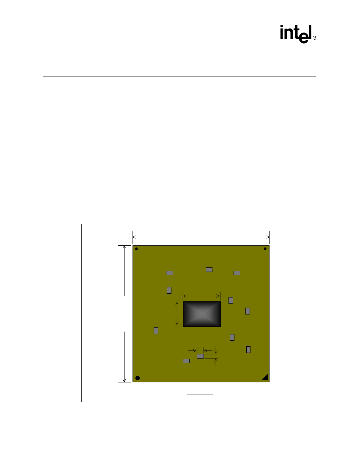
Mechanical Reference
Mechanical Reference 2
The Intel® 855GME and Intel 852GME chipset MCHs are constructed with a Flip Chip Ball Grid
Array (FCBGA) package with a size of 37.5 mm x 37.5 mm. It includes 732 solder ball lands with
a ball pitch of 1.27 mm. The chipset MCH will also include capacitors moun ted on the top of the
package. Reference drawings are shown in Figure 1 and Figure 2. The drawings are not drawn to
scale and the units shown are in millimeters.
The 855GME and 852GME MCH packages will include capacitors on the top-side. The location of
capacitors may differ between the 855GME and 852GME MCHs. Care should be taken when
applying a thermal solution onto the die in order to avoid any accidental electrical shorts.
2.1 Intel® 855GME and Intel® 852GME Chipset MCH Package
Note: The capacitor locations shown below may not be representative of the exact placement on the
855GME or the 852GME MCH.
Figure 1. 855GME and 852GME chipset MCH Package Dimensions (mm) – Top View
37.5
37.5
Capacitor
Capacitor
7.6
7.6
37.5
37.5
10.3
10.3
1.60
1.60
Die
Die
Substrate
Substrate
0.81
0.81
?
?
Top View
Top View
8 Intel® 855GME and Intel® 852GME Thermal Design Guide for Embedded Applications
Page 9
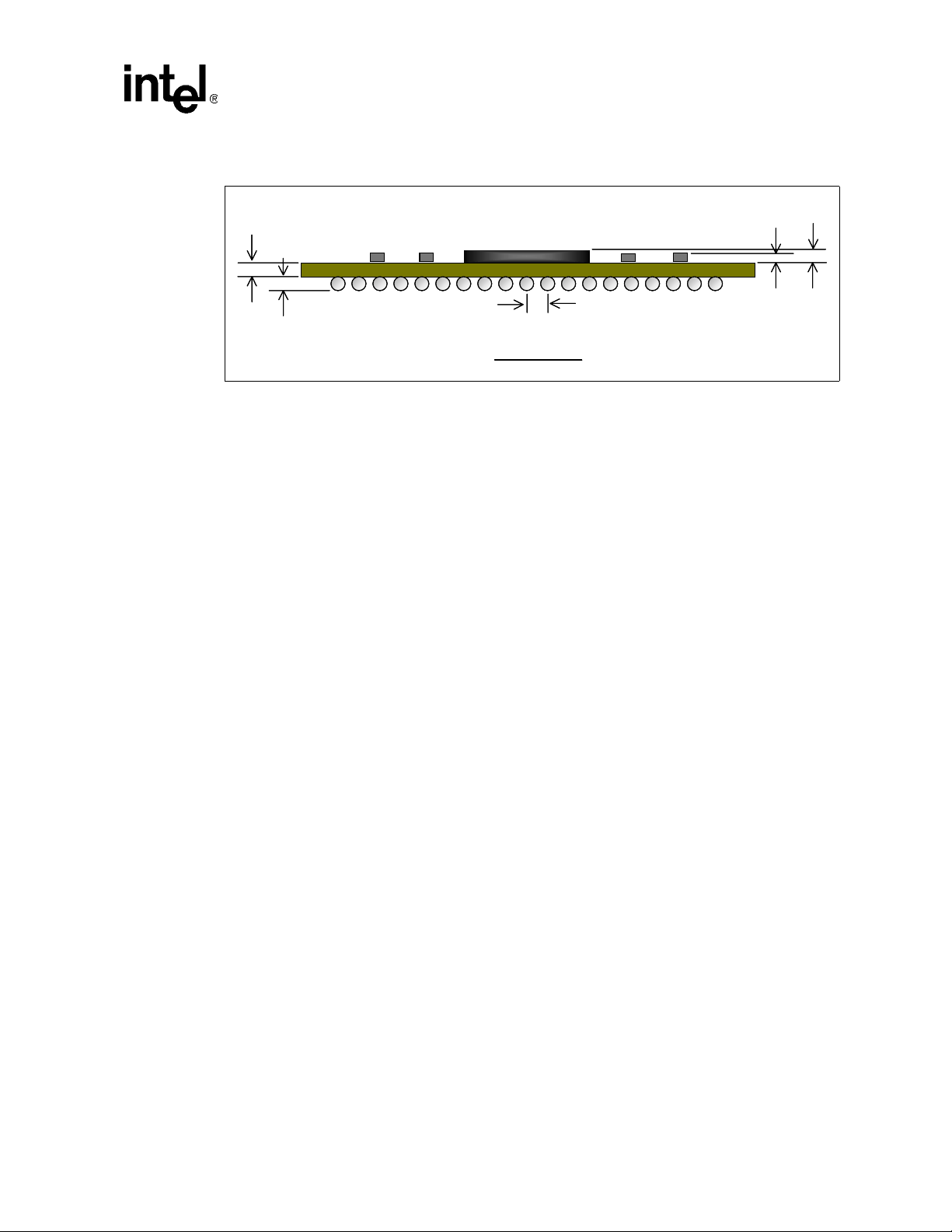
Mechanical Reference
Figure 2. 855GME and 852GME Chipset MCH Package Dimensions (mm) - Side View
1.0
1.0
0.61
0.61
0.7
0.7
1.27
1.27
Side View
Side View
0.73
0.73
Intel® 855GME and Intel® 852GME Thermal Design Guide for Embedded Applications 9
Page 10
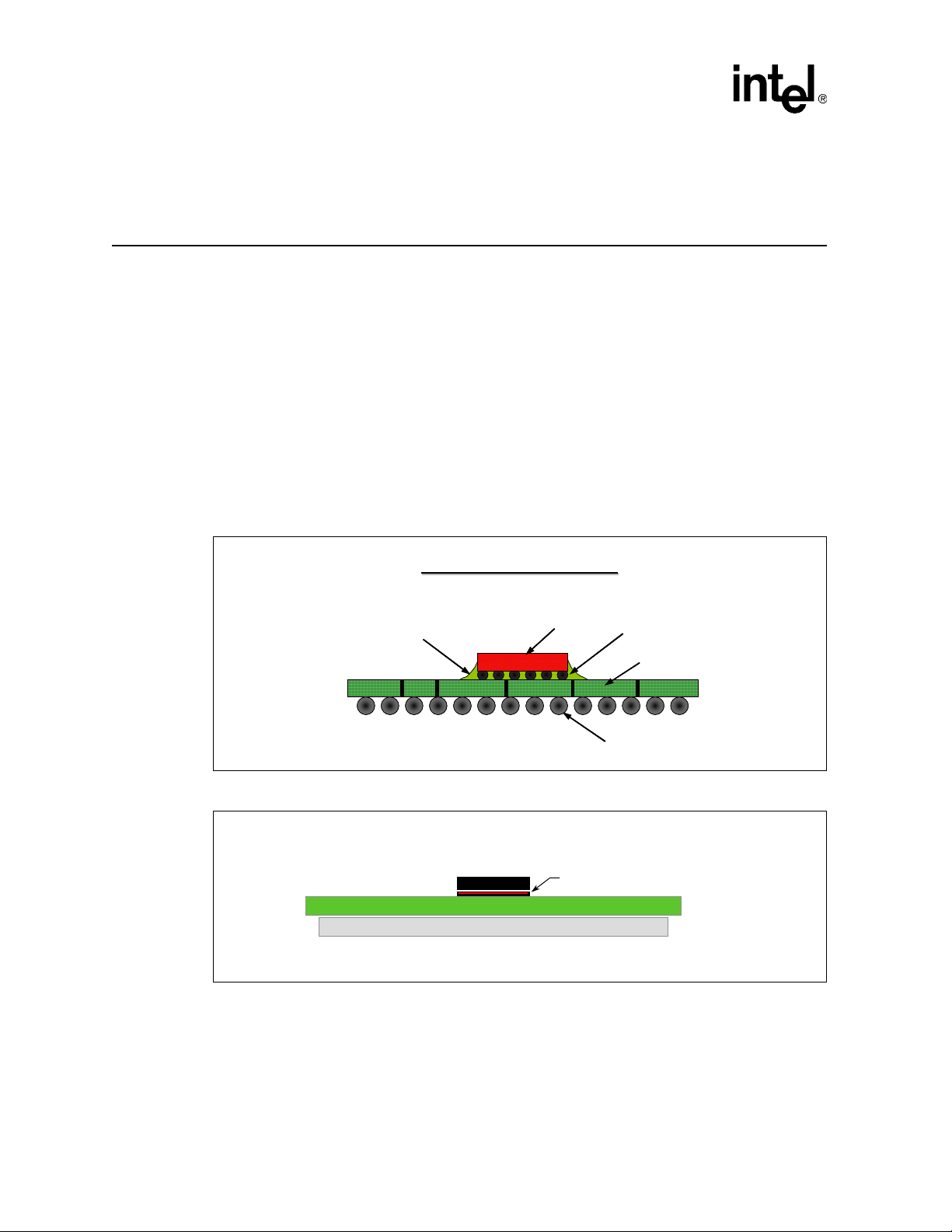
Computational Fluid Dynamics (CFD) Modeling
Computational Fluid Dynamics (CFD)
Modeling 3
3.1 855GM MCH Thermal Model
A Computational Fluid Dynamics (CFD) thermal model of the 855GM chipset MCH has been
developed to assist in the characterization of the package thermal limits and the evaluation of
cooling methods. The thermal model used in our analysis is based on the package construction
shown in Figure 3. Simplified cuboids with the correct material properties are used to model the
primary portions of the chipset MCH package as shown in Figure 4. Contact your Intel
representative for information on obtaining the CF D model.
Note: The CFD thermal model for the 855GM MCH may als o be us ed for the 8 55GME and t he 852G ME
chipset MCHs.
Figure 3. Package Construction Overview
Underfill
Underfill
Figure 4. 855GM MCH Thermal Model
Package Overview
Package Overview
Package Overview
Package Overview
Die
Die
855GM Thermal Model
Die
Substrate
Solder Balls
C4
C4 bumps
C4 bumps
Substrate
Substrate
Solder balls
Solder balls
B1998-01
10 Intel® 855GME and Intel® 852GME Thermal Design Guide for Embedded Applications
Page 11

Computational Fluid Dynamics (CFD) Modeling
3.2 Thermal Design Power (TDP) Values
Use the following thermal design power (TDP) values when modeling based on the configuration
that is being simulated. When designing for intermediate configu r ations o n the 855GME MCH,
round up to next highest TDP value.
T able 2. 855GME and 852GME MCH Thermal Design Power
SKU Config
®
855GME
Intel
MCH
Intel® 852GME
MCH
Core
VCC (V)
Max 1.35 250 333 512 2 4 Dual 4.3
Min 1.2 133 200 256 1 1 Single 2.6
Max 1.5 266 333 512 2 4 Dual 5.7
GFX
Core
(MHz)
DDR
(MHz)
Memory
Size
(Mbytes)
# of
DIMMs
# of
Rows
3.3 Maximum Temperature Specification
Use the following table to determine the maximum junction temperature value when modeling the
855GME or 852GME chipset MCH. The junction temperature is located at the hottest part of the
die.
T a ble 3. 855GME and 852GME Chipset MCHs Maximum Temperature Value
Tj,max (°C)
110
3.4 Modeling Assumptions
Computational Fluid Dynamics (CFD) modeling is performed to provide a basis for estimating the
behavior of the Intel
configurations. Intel provides a Flotherm model of the 855GM and is available through field
sales. This model may also be used to simulate the 855GME and 852GME chipset MCHs. The
thermal model of the Intel
simulated CompactPCI* blade environment. Assumptions used in the thermal analyses are
summarized below. However, please note that they do not represent a specific design
recommendation and are mainly used as a basis for the thermal analysis.
®
855GME and Intel® 852GME chipset MCHs under varying cooling
®
855GME and Intel® 852GME chipset MCHs were analyzed in a
LVDS
Display
Settings
TDP
(W)
The following analysis was performed to evaluate the need for a heatsink to adequately cool the
855GME and 852GME chipset MCHs.
Thermal Modeling Ass umptions
:
1. Local Ambient Conditions between 40º C and 60º C. Local ambient is specified as the
temperature locally surrounding the processor. Most local ambient conditions for embedded
applications fall near the middle of that range.
2. Airflow ranges between 50 and 500 LFM.
3. The entire motherboard is modeled as an orthotropic cuboid with an effective thermal
conductivity based on the assumed copper content of the motherboard. In the analysis
Intel® 855GME and Intel® 852GME Thermal Design Guide for Embedded Applications 11
Page 12
Computational Fluid Dynamics (CFD) Modeling
T
°
presented the copper content is assumed to be 10 percent of the overall volume of the
motherboard.
4. Board-to-board spacing of 0.8”, consistent with the CompactPCI* specification.
5. Tj,max for the 855GME and 852GME chipset MCHs is 110 °C.
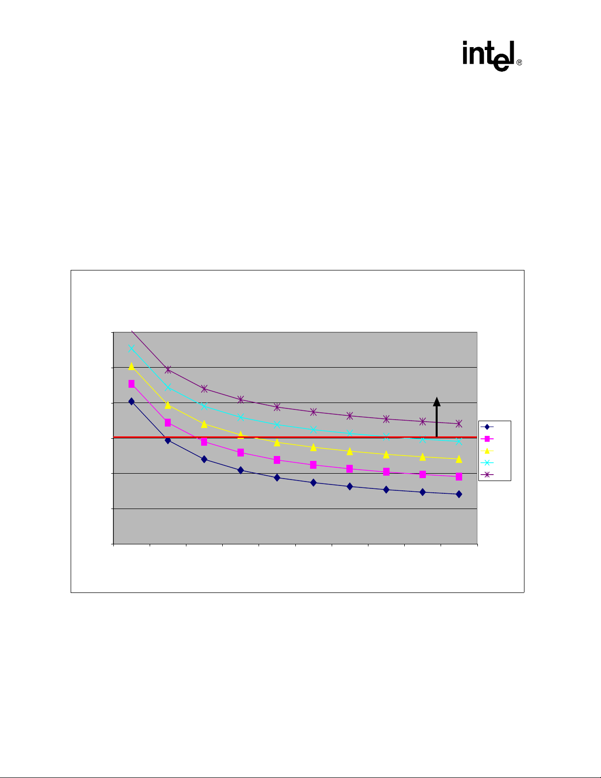
3.5 Modeling Results – 855GME MCH
Some boundary conditions evaluated will necessitate a heatsink for the 855GME chipset MCH.
See Figure 5 for a graph of junction temperature (Tj) vs. airflow (in linear feet per minute) for
various local ambient temperature conditions. A heatsink will be needed in all cases where the Tj
of the 855GME chipset MCH die is greater than 110 °C.
Figure 5. 855GME MCH (4.3W) Junction Temperatures vs. Airflow
855GM E (4.3W ) Junction Temperatures vs. Airflow
at Various Local Am bient Tem peratures
140
130
Heatsink
Required
120
40 C
110
Tj (deg C)
100
90
80
50 100 150 200 250 300 350 400 450 500
Airflow (LFM)
j max = 110
C
45 C
50 C
55 C
60 C
12 Intel® 855GME and Intel® 852GME Thermal Design Guide for Embedded Applications
Page 13

Computational Fluid Dynamics (CFD) Modeling
T
3.6 Modeling Results – 852GME
All boundary conditions evaluated will necessitate a heatsink for the 852GME chipset MCH. See
Figure 6 for a graph of junction temperature (Tj) vs. airflow for various local ambient temperature
conditions. A heatsink will be needed in all cases where the Tj of the 852GME chipset MCH die
is greater than 110 °C. Notice that a heatsink is necessary for all cases shown below.
Figure 6. 852GME Airflow Modeling Results
852GME (5.7W) Junction Temperatures vs. Airflow
at Various Local Ambient Temperatures
160
150
140
130
Tj (deg C)
120
110
100
50 100 150 200 250 300 350 400 450 500
Airflow (LFM)
3.7 CFD Modeling Conclusions
j max = 110
Heatsink
Required
40 C
45 C
50 C
55 C
60 C
°C
The 855GME chipset MCH, under many embedded configurations, will not require a heatsink.
However, if your boundary conditions are not sufficient to adequately cool the chipset MCH, Intel
offers two reference heatsink designs which are found in sections 4 and 5.
The 852GME chipset MCH will require a heatsink under almost all configurations. Refer to
sections 4 and 5 for a reference thermal solution developed by Intel. Both solutions will work with
the 852GME.
Intel® 855GME and Intel® 852GME Thermal Design Guide for Embedded Applications 13
Page 14

Reference Thermal Solution for 1U Applications
Reference Thermal Solution for 1U
Applications 4
4.1 Applications
The thermal solution referenced in this chapter is valid for both the 855GME and 852GME when
the system allows for upwards of 1U (1.75” chassis) in z-height.
Note: Many boundary conditions may permit the 855GME MCH heatsink to be packaged without a
thermal solution. The 852GME will require a heatsink in most configurations. See Section 3 for
computational fluid dynamics (CFD) modeling where specific boundary conditions are analyzed.
The reference thermal solution is capable of adequately cooling the 855GME or 852GME chipset
MCHs at all boundary conditions referenced in Section 3.4.
4.2 Required Volumetric Keepout
The 1U thermal solution will require a volumetric keepout region above the chipset MCH. See
Figure 7 for a detailed side and top view of the keepout.
Appendix B, “Mechanical Drawings” contains a detailed board keep-out restriction for the
heatsink a nd mounting clips.
Note that the 1U reference thermal solution for embedded applications is exactly the same as that
referenced in the thermal design guide for the Intel® 845G chipset MCH. See Table 1 for location
of the Intel® 845G Chipset MCH Thermal Design Guide.
14 Intel® 855GME and Intel® 852GME Thermal Design Guide for Embedded Applications
Page 15

Reference Thermal Solution for 1U Applications
Figure 7. 1U Reference Thermal Solution Volumetric Keepout
Intel® 855GME and Intel® 852GME Thermal Design Guide for Embedded Applications 15
Page 16

Reference Thermal Solution for 1U Applications
4.3 Heatsink Assembly
The 1U heatsink assembly includes the heatsink (with thermal interface material (TIM) and
mechanical interface gasket), the clip, and clip lever as shown in Figure 8. This clip attaches to
solder down anchors located on the system board.
Figure 9 shows the assembly placement and actuation mechanism.
Figure 8. 1U Heatsink Assembly (Heatsink, Clip Frame, and Clip Lever)
Figure 9. 1U Heatsink Assembly Placement and Actuation
16 Intel® 855GME and Intel® 852GME Thermal Design Guide for Embedded Applications
Page 17

4.4 Mechanical Retention
The heatsink is affixed to the die with a mechanical advantage clip. The clip consists of a clip
frame that interfaces to the motherboard through four through-hole mount anchors and an integral
lever (see Figure 12). The clip and lever serve three main purposes:
• Secure the heatsink in intimate contact with the die
• Ensure a thermally good baseline between the die and heatsink
• Prevent damage at the package-to-motherboard solder joint during mechanical shock events
The heatsink must maintain close contact with the die for the life of the system. The generic clip
retention mechanism design holds the heatsink to the die through a single point of contact at the
center of the heatsink. This ensures that the clip load is centered on the die, thus preventing
heatsink tilt that may be caused by unbalanced loading. The clip frame also restrains heatsink
lateral motion through tabs located between the heatsink fins (see Figure 11).
Figure 10. 1U Heatsink Clip Assembly
Reference Thermal Solution for 1U Applications
Intel® 855GME and Intel® 852GME Thermal Design Guide for Embedded Applications 17
Page 18

Reference Thermal Solution for 1U Applications
Figure 11. 1U Heatsink Clip Lateral Retention Tab Feature
4.5 Thermal Interface Material (TIM) and Thermal Bond Line
A thermal interface material (TIM) is used to provide improved conductivity between the die and
heatsink. The reference thermal solution uses Chomerics* T-710, 0.127 mm (0.005”) thick,
12.7 mm x 12.7 mm (0.5” x 0.5”).
The thickness of the bond line between the heatsink and die is critical to the thermal performance
of the TIM. The bond line thickness is dep enden t on the pres sure b etween the heatsink and the die.
The clip retention mechanism is used to generate the pressure required to ensure the thermal
performance required. The generic clip frame and lever design generates more than 50-psi
pressure.
4.6 Solder Joint Protection
The generic clip design uses mechanical preload on the package to protect the solder joint against
damage under mechanical shock. The design features a rotating cam (s ee Figure 12) that generates
substantial preload between the heatsink and package. The cam has a levered handle that provides
a mechanical advantage during installation.
The preload serves to compress the solder ball array between the package and the motherboard.
The compression in the solder balls delays the onset of the tensile load under critical shock
conditions, and the magnitude of the maximum tensile load is thereby reduced. In this manner, the
critical solder balls are protected from tensile loading that may cause damage to the solder joint.
18 Intel® 855GME and Intel® 852GME Thermal Design Guide for Embedded Applications
Page 19

Reference Thermal Solution for 1U Applications
Figure 12. 1U Heatsink Clip Frame and Lever
4.7 1U Reference Thermal Solution Mechanical Drawings
Contact your field representative for additional information.
Note: The 1U reference thermal solution presented in this chapter is the same as that referenced in the
®
Intel
845G Chipset MCH Thermal Design Guide.
Intel® 855GME and Intel® 852GME Thermal Design Guide for Embedded Applications 19
Page 20

Reference Thermal Solution for CompactPCI* and Blade Applications
Reference Thermal Solution for
CompactPCI* and Blade Applications 5
5.1 Applications
The thermal solution referenced in this chapter is valid for both the 855GME and 852GME chipset
MCHs when the application only allows for 0.54” of z-height above the board. Note that many
boundary conditions may permit the 855GME MCH to be packaged without a thermal solution.
The 852GME will require a heatsin k in mo st confi gurations . See Chapter 3 for computational fluid
dynamics (CFD) modeling where specific boundary conditions are analyzed.
5.2 CompactPCI* Heatsink Thermal Performance
The CompactPCI reference thermal solution is capable of adequately cooling the 855GME or
852GME chipset MCHs at most boundary conditions referenced in Section 3.4.
Figure 13 below shows the thermal performance of the heatsink on both the 855GME and
852GME MCHs at a local ambient temperature (T
ambient temperatures, shift the curve vertically upwards or downwards accordingly. Note that at
T
=60°C with 50 LFM of airflow, this heatsink may not adequately cool the 852GME. For these
LA
applications, Intel recommends the use of the 1U thermal solution presented in Ch apter 4.
) of 55 °C. For performance at other local
LA
20 Intel® 855GME and Intel® 852GME Thermal Design Guide for Embedded Applications
Page 21

Reference Thermal Solution for CompactPCI* and Blade Applications
Figure 13. CompactPCI* Heatsink Thermal Performance
Tcase Temperature (deg C)
855GME/852GME Tcase vs. Airflow for CompactPCI Heatsink
at Tem perat ur e (local ambien t) = 55 d e g C
120
110
Tcas e ma x = 105 deg C
100
90
80
70
60
50 100 150 200 250 300 350 400 450 500
Airflow (LFM)
Tcase for
855GME
(4.3W)
Tcase for
852GME
(5.7W)
5.3 Required Volumetric Keepout
The CompactPCI* thermal solution will require a volumetric keepout region above the chipset
MCH. See Figure 14 for a detailed side and top view of the keepout.
There is not a board keep-out restriction for the CompactPCI* heatsink. It uses an adhesive tape
thermal interface material for mechanical retention, and is smaller in footprint than the 855GME
and the 852GME chipset MCHs.
Intel® 855GME and Intel® 852GME Thermal Design Guide for Embedded Applications 21
Page 22

Reference Thermal Solution for CompactPCI* and Blade Applications
Figure 14. CompactPCI* Thermal Solution Volumetric Keepout
5.4 CompactPCI* Heatsink Assembly
The CompactPCI heatsink assembly includes the heatsink an adhesive tape thermal interface
material, and a protective pull-tab as shown in Figure 15 on page 23.
22 Intel® 855GME and Intel® 852GME Thermal Design Guide for Embedded Applications
Page 23

Reference Thermal Solution for CompactPCI* and Blade Applications
Figure 15. CompactPCI* Heatsink Assembly (Heatsink, Pull-tab, and TIM)
Note: Thermal Interface Material (TIM) is not shown in picture.
5.5 Mechanical Retention
The heatsink is affixed to the die with an adhesive tape thermal interface material. This retention
scheme does not require board modifications and can be incorporated at any point in the design
cycle, assuming the z-height requirement is met.
5.6 Thermal Interface Material (TIM) and Thermal Bond Line
A thermal interface material (TIM) is used to provide improved conductivity between the die and
heatsink. The reference thermal solution uses Chomerics* T411 adhesive tape thermal interface
material, 15 mm x 15 mm x 0.254 mm (0. 59” x 0.59” x .01”).
The thickness of the bond line between the heatsink and die is critical to the thermal performance
of the TIM. The bond line thickness is d epend ent o n th e pres sure between th e heats ink and the die.
It is imperative that the heatsink is applied to the die with adequate force.
Intel® 855GME and Intel® 852GME Thermal Design Guide for Embedded Applications 23
Page 24

Reference Thermal Solution for CompactPCI* and Blade Applications
For more information on force required and other important documentation, see the Chomerics
website at http://www.chomerics.com.
5.7 CompactPCI* Thermal Solution Mechanical Drawings
See Appendix B, “Mechanical Drawings” for a detailed drawing.
For an official electronic copy, contact Foxconn*. Contact information is available in Appendix A,
“Vendor Information”.
24 Intel® 855GME and Intel® 852GME Thermal Design Guide for Embedded Applications
Page 25

Temperature Measurement Metrology
Temperature Measurement Metrology 6
6.1 Case Temperature Measurements
Intel has established guidelines for the prop er techn iques to be us ed when measuring chip set MCH
case temperature. Section 7.3 contains information on running an application program that
emulates anticipated TDP.
The surface temperature at the geometric center of the die corresponds to the maximum Tcase.
6.2 0 Degree Angle Attach Methodology
1. Mill a 3.3 mm (0.13”) diameter hole centered on bottom of the heatsink base (see Figure 5).
The milled hole should be approximately 1.5 mm (0.06”) deep.
2. Mill a 1.3 mm (0.05”) wide slot, 0.5 mm (0.02”) deep, from the centered hole to one edge of
the heatsink. The slot should be in the direction parallel to the heatsink fins (see Figure 16 and
Figure 17).
3. Attach thermal interface material (TIM) to the bottom of the heatsink base.
4. Cut out portions of the TIM to make room for the thermocouple wire and bead. The cutouts
should match the slot and hole milled into the heatsink base.
5. Attach a 36 gauge or smaller calibrated K-type thermocouple bead or junction to the center of
the top surface of the die using a high thermal conductivity cement. During this step, make
sure there is no contact between the thermocouple cement and the heatsink base because any
contact will affect the thermocouple reading. It is critical that the thermocouple bead makes
contact with the die (see Figure 17).
6. Attach heatsink assembly to the MCH and route the thermocouple wires our through the
milled slot.
Intel® 855GME and Intel® 852GME Thermal Design Guide for Embedded Applications 25
Page 26

Temperature Measurement Metrology
Figure 16. 0 Degree Angle Attach Heatsink Modifications (not to scale
Figure 17. 0 Degree Angle Attach Methodology (not to scale)
6.3 Maximum Temperature Specification
Use Table 4 to determine the maximum temperature value when performing thermal labor a to ry
testing with the 855GME or 852GME chipset MCH using the metrology described in this chapter
and the TDP Stress Application. More information about the TDP stress application may be found
in Section 7.
Table 4. 855GME and 852GME chipset MCH Maximum Case Temperature Value
Tcase,max (°C)
105
26 Intel® 855GME and Intel® 852GME Thermal Design Guide for Embedded Applications
Page 27

Thermal Management Features and Tools
Thermal Management Features and
Tools 7
7.1 Internal Temperature Sensor
The Intel 855GME and 852GME chipset MCH will include an on die temperature sensor that can
be used to protect the chipset MCH from exceeding the Tj,max specification. Upon detection that
the sensor has reached Tj,max the chipset MCH will be capable of initiating a bandwidth throttling
event that will reduce chipset MCH power and temperature. The sensor will also prove to be useful
in optimizing the thermal design for the chipset MCH by being able to provide jun c tio n
temperature during testing and evaluation of the thermal solution.
7.2 External Temperature Sensor
The chipset MCH is designed to accept an input signal from an external temperature sensor. The
external sensor can be placed in a location close to the DDR memory and upon detecting a “hot”
condition the chipset MCH would throttle the READ bandwidth. Proper placement of the sensor
would have to be determined by the OEM. The OEM would have to characterize the temperature
difference between the sensor and the DDR memory devices to determine the best placement for
the sensor. On detection of a “hot” condition a signal is communicated directly from the thermal
sensor to t he MCH via the ETS# pin as shown in Figure 18. The external thermal sensor can be
programmed via the SMBus.
Figure 18. External Temperature Sensor
ETS#ETS#
CPU
MCH-M
ICH
SMBus
THERM#
SO-DIMM’s
TS TS
Thermal Sensor on
motherboard. OEM
design dependent
SMBdata
SMBclock
Intel® 855GME and Intel® 852GME Thermal Design Guide for Embedded Applications 27
Page 28

Thermal Management Features and Tools
7.3 TDP chipset MCH Stress Application
Intel provides a TDP stress software tool that can be used to validate chipset MCH thermal
solutions. The software tool will generate high memory write bandwidths to stress the chipset
MCH. The usage model for this software will include the following steps:
1. During the validation phase, OEMs will run this program on their platforms under worse case
system loading and environmental conditions. Worse case conditions might include things
such as loading the maximum number of rows for memory, setting the operating system to
maximum performance mode, an ambient environment at 55º C, and a still air environment
with no external air drafts.
2. Th e TDP stress application will remain running and the junction temperature will be
monitored until it has reached steady state. At the completion of the test, if the junction
temperature of the chipset MCH does not exceed the maximum operating temperature (110º C)
then the thermal solution can be deemed as adequate.
3. If the junction temperature exceeds the maximum operating temperature then this will provide
an indication that the thermal solution needs to be improved. Modifications to the thermal
solution should be made and the system should be retested until th e appr opriate junction
temperature can be maintained.
The TDP application will also allow the OEM to determine appropriate bandwidth WRITE throttle
settings to program into the BIOS.
7.4 Memory Thermal Management Software
The Intel Memory Thermal Management Software is a software application that allows OEMs to
generate high memory read bandwidths to stress memory. The usage model for this software will
include the following steps:
1. Preparation before testing will include placing thermocouples on each of the memory devices
of the DDR DIMMs that are to be used during validation.
2. During the validation phase, OEMs will run this program on their platforms under worse case
system loading and environmental conditions. Worse case conditions might include things
such as loading the maximum number of rows for memory, setting the operating system to
maximum performance mode, an ambient environment of 55 ºC, and a still air environment
with no external air drafts.
3. Th e pro gram will allow the OEM system designer to test at several different bandwidth
throttle settings. Some of the typical settings available for previous chipset MCHs were 65
percent, 55 percent, and 45 percent of the maximum write bandwidth. Th e OEM can begin by
running the test at one of the low bandwidth settings and monitoring the temperatures on the
DDR DIMMs. The temperatures should be allowed to reach steady state.
4. Once the temperatures are at steady state the OEM can observe the data and determine whether
any of the temperatures have exceeded the maximum allowable temperature for the memory
devices. If all the temperatures are within the allowed specification then the OEM can proceed
to the next test at a higher bandwidth setting.
5. Th is process will be repeated until the OEM tests at a bandwidth throttle setting that causes
temperature specifications to be exceeded for either the memory devices o r the bottom su rface.
This bandwidth limit will be used to determine the appropriate memory READ throttle setting
that can be programmed into the BIOS.
28 Intel® 855GME and Intel® 852GME Thermal Design Guide for Embedded Applications
Page 29

Thermal Management Features and Tools
7.5 Thermal Throttling
Both the Intel 855GME and Intel 852GME chipset MCHs are available with throttling
functionality to protect the chipset MCH from power virus conditions that can cause junction
temperatures to increase beyond maximum allowable junction temperatures. Two different
methods of thermal throttling are available on the chipset MCH: bandwidth triggered and
temperature based throttling.
There are three important things to remember about throttling:
1. It is only intended to be a safeguard to ensure that junction temperatures do not exceed
maximum specified junction temperatures.
2. chipset MCH thermal solutions must still be designed to TDP. Thro ttling is not recommended
as a method of designing the chipset MCH cooling capability to levels below TDP.
3. This mechanism was carefully designed to have minimal impact on real applications, while
safeguarding against harmful synthetic applications. However, throttling may affect
performance of the chipset MCH. Performance of the chipset MCH should be verified by
testing with benchmarks.
7.5.1 Bandwidth Triggered Throttling
Bandwidth triggered throttling will limit the max im um bandwidth that can be sustained over long
periods as a safeguard against a thermal virus. This method of thermal management will
temporarily decrease bandwidth performance of the chipset MCH when an application demands
large, sustained bandwidth levels that could cause the chipset MCH to exceed its maximum
junction temperature. However, in order to trigger bandwidth throttling, the chipset MCH
bandwidth must exceed the threshold over an entire sampling window. Most applications use high
bandwidths only in short bursts, and through application analysis, this sampling window has been
set large enough so that these applications that create short bursts in bandwidth will not see any
throttling. Only a sustained high bandwidth for a period longer than the sampling w indo w has the
potential of exceeding thermal limits, and the throttle mechanism is designed to protect the chip
against those potentially harmful applications.
Figure 19 below provides a theore tical example of h ow ban dwidth th rottling would work. In this
example, the bandwidth is set to throttle at 1100 MB/sec. The throttling value would be determined
based on the worst case operating conditions. This throttle setting is enabled upon system boot and
only one value can be set for the WRITE operatio ns of th e chips et MC H. To determine bandwidth,
the read/write operations are being monitored continuously by hardware insid e the chipse t MCH
within a one second window.
Intel® 855GME and Intel® 852GME Thermal Design Guide for Embedded Applications 29
Page 30

Thermal Management Features and Tools
Figure 19. 855GME/852GME chipset MCH Bandwidth Throttling
1. The system is operating at an idle workload until an application that requires a large amount of
bandwidth is initiated. The application demands a peak bandwidth of 1200 MB/sec. for an
entire sampling window interval, and it will be reduced to the bandwidth throttle setting limit
of 1100 MB/sec. The throttle setting of 1100 MB/sec. ef fectively places a cap on the allowable
bandwidth.
Note: Applications are still allowed to exceed the 1100 MB/sec. limit in short bursts that last less than the
sampling window period.
2. Th e chi ps et MCH will continue to operate at the throttled amount of 1100 MB/sec. until the
application no longer requires this level of sustained bandwidth. In this case the junction
temperature has not increased to a temperature that is close to the maximum junction
temperature limit of 110º C. So it appears that for the brief period that the large bandwidth
level was required the chipset MCH was unnecessarily throttled. A drawback of using
bandwidth triggered throttling is that under certain conditions when the system is not operating
under worse case conditions the chipset MCH will be throttled regardle ss of the junction
temperature.
3. Once the application stops the system workload will return to a lower workload.
30 Intel® 855GME and Intel® 852GME Thermal Design Guide for Embedded Applications
Page 31

Thermal Management Features and Tools
7.5.2 Temperature Triggered Throttling
Temperature triggered throttling will limit the maximum achievable bandwidth as a safeguard
against a thermal virus only when the junction temperature reaches a specified trip point
temperature. This method of thermal throttling is an improvement over the bandwidth
triggered throttling method because the chipset MCH will only reduce bandwidth
performance when it is absolutely necessary under a preset condition.
The temperature throttle trip point is programmed into the chipset MCH at boot. If the temperature
of the chipset MCH goes beyond the trip point limit, the chipset M CH will be throttled to a
predetermined maximum throttling amount until the temperature drop s be low the same
temperature limit.
Figure 20 below provides an example of ho w temper ature triggered throttling would optimize
throttling under conditions similar to the scenario that was descr ibed in Section 7.5.1. In this
scenario the hot trip temperature is set at 100 ºC . Keep in mind that th e Tj,max specification f or the
855GME and 852GME chipset MCHs is 110 ºC and the example described in the section is only
intended to illustrate the behavior. The hot trip temperature represents the temperature setpoint at
which the chipset MCH will initiate throttling.
Figure 20. 855GME/852GME chipset MCH Temperature Throttling
1. The system is operating at an idle workload until an application that requires a large amount of
bandwidth is initiated. The application demands a peak bandwidth of 1200 MB/sec. and the
chipset MCH will sustain this bandwidth leve l until the temperature climbs above the hot trip
setting of 100 ºC.
2. During this test the chipset MCH operates at a 1200 MB/sec. bandwidth level for a period
longer than the sampling window because the junction temperature has not increased above
the hot trip point setting. In this case the chipset MCH is demonstrati ng better bandwidth
performance while operating under the same application as in the bandwidth triggering case.
This is clearly a preferred method of throttling the chipset MCH only when it is absolutely
necessary.
Intel® 855GME and Intel® 852GME Thermal Design Guide for Embedded Applications 31
Page 32

Thermal Management Features and Tools
3. Once the application stops the system workload will return to its idle level of 200 MB/sec. In
this example, the chipset MCH never required any thermal throttling. The method will
potentially allow for large, brief bursts of bandwidth loading without impeding chipset MCH
performance.
32 Intel® 855GME and Intel® 852GME Thermal Design Guide for Embedded Applications
Page 33

Thermal/Mechanical Applications
Thermal/Mechanical Applications 8
8.1 Thermal Interface Materials
Use of a Thermal Interface Material (TIM) between the chipset MCH package and the thermal
enhancement is highly recommended to reduce the thermal resistance b etween the package an d the
thermal enhancement device. A reduction in the thermal resistance at this interface creates a larger
effective thermal conductivity through the interface that improves the thermal capability of the
package.
Common types of interface materials include elastomers and phase change materials. These types
of materials can easily conform to fill small air gaps that are left between the two interfaces that are
mated together. These air gaps can act as insulators and will increase the thermal resistance. An
interface material can assist in filling these voids and reducing the thermal resistance at the
interface. The total thermal resistance through the interface would consist of the three main
resistances:
1. Thermal interface material resistance (θ
2. Contact resistance between the top of the chipset MCH package and the bottom of the ther mal
interface material (θ
3. Contact resistance between the top of the thermal interface material and the bottom of the heat
spreader or heat sink (θ
contact-top
)
contact-bottom
TIM
)
8.1.1 Estimate Thermal Resistance
The thermal resistance of a material can be estimated by using the expression in Equation 1.
The expression provides a result in units of ºC/W. If adequate force is applied onto the thermal
interface material, it can be assumed the contact resistances are negligible. This is a valid
assumption when using the reference design described in Section 4.
Equation: Thermal resistance of a material
θ
TIM
θ
= Thermal Resistance through the material (ºC/W)
TIM
L = thickness of the material (m)
)
L
=
kA
k = thermal conductivity of material (W/m-ºC)
A = cross sectional area of the material (m
Intel® 855GME and Intel® 852GME Thermal Design Guide for Embedded Applications 33
2
)
Page 34

Thermal/Mechanical Applications
8.2 Mechanical Loading
The pressure applied to the surface of the 855GME or 852GME MCH package should not exceed
100 psi.
If the pressure on the surface of the chipset MCH package is exceeded, problems may arise. The
solder ball joints between the package and the motherboard may be subjected to fractures that
could result in a loss or degradation of electrical signals from the chipset MCH. Also, the die may
be exposed to warpage or, at unusually high levels of stress, cracking.
If a large compressive load is applied to the die surface precautions should be taken to help
alleviate some of the load. One manner of doing this is to provide some backing support for the
motherboard directly underneath the chipset MCH. Standof fs can be used between the motherboard
and the chassis to add rigidity to the motherboard under the chipset MCH and reduce the amount of
board flexure under larg e loads.
8.3 Thermal and Mechanical Reliability
Recommendations for thermal mechanical reliability testing are shown in Table 5. These should be
considered as genera l guideline s. The user should define validation testing requireme nts based on
anticipated use conditions.
Table 5. Reliability Validation
(1)
Test
Mechanical Shock
Random Vibration
Power Cycling (for
active solutions)
Thermal Cycling
Humidity
NOTES:The above tests should be performed on a sample size of at least 12 assemblies from 3 different lots
of material.
Additional Pass/Fail Criteria may be added at the discretion of the user.
Requirement Pass/Fail Criteria
• Quantity: three drops for + and – directions in each
of three perpendicular axes (i.e., total of 18 drops).
• Profile: 50 G trapezoidal waveform, 11 ms duration,
170 in/s minimum velocity change.
• Setup: Mount sample board on test fixture
• Duration: 10 min/axis, three axes
• Frequency Range: 5 Hz to 500 Hz
• Power Spectral Density (PSD) Profile: 3.13 G RMS
• 7500 on/off cycles with each cycle specified as 3
minutes on, 2 minutes off at 70 °C
• -5 °C to +70 °C, 500 cycles Visual Check
• 85% relative humidity, 55 °C, 1000 hours Visual Check
Visual Check and Electrical
Functional Test
Visual Check and Electrical
Functional Test
Visual Check
(2)
34 Intel® 855GME and Intel® 852GME Thermal Design Guide for Embedded Applications
Page 35

Summary
Summary 9
The Intel® 855GME and Intel® 852GME Chipset Memory Controller Hub (MCH) Thermal Design
Guide For Embedded Applications was developed to aid in creating adequate thermal design s th at
will insure reliable and efficient operation of the 855GME and 852GME chipset MCHs in
embedded applications. The goal of this document is to pr ovide an understanding of the operating
limits of the chipset MCH in embedded environments and to recommend proper thermal design
techniques based on a particular configuration.
Computational Fluid Dynamics (CFD) analysis proved to be a useful tool in provid ing an initial
basis to determine the thermal limits of the chipset MCH under varying cooling configurations.
Developing a CFD analysis early in the d esign stage is h ighly recom mended to assist in iden tifying
potential thermal issues at the individual component and system levels.
Several new features and tools will be made available with the 855GME and 852GME chipset
MCH. The chipset MCH will have an on die temperature sensor to assist the thermal control and
validation of the thermal solution. It will also have the capability to resp ond to an input from an
external temperature sensor that is placed next the DDR DIMMs. This will allow for improved
thermal control of memory temperatures. New software tools will also be provided to validate the
thermal solution design at TDP levels and to determine read/write throttle settings.
Intel® 855GME and Intel® 852GME Thermal Design Guide for Embedded Applications 35
Page 36

Vendor Information
Vendor Information A
Table 6. 1U Reference Design Heatsink Assembly Suppliers (as referenced in Section 4)
Part
Extruded
Heatsink
Interface
Materials
Attach
Hardware
Entire
Enabling
Assembly
NOTE: The above reference heatsink vendors and information are identical to that of the Intel
Pin Fin Heatsink A54515-001 Foxconn*
Chomerics Phase Change
TIM (T-710)
Mechanical Interface Material
(Poron)
Clip Frame A65066-001 Foxconn
Clip Lever A67031-001 Foxconn
Solder-Down Anchor (4
required per heatsink)
MCH Enabling Assembly
Includes:
Pin fin heatsink, thermal
interface material, mechanical
interface material, clip frame,
and clip lever (does not
include solder-down anchors)
Intel Part
Number
A61203-001 Boyd*
A13494-005 Foxconn HB96030-DW
A67625-001 Foxconn PHC029C02012
Supplier
Chomerics* 69-12-22066-T710
Supplier Part
Number
®
845G MCH.
T a ble 7. CompactPCI* Reference Design Heatsink Assembly Suppliers (as referenced in
Section 5)
Part
Entire Extruded
Heatsink Enabling
Assembly
Heatsink Only Pin Fin Heatsink N/A Foxconn 071-0000-884-1
Thermal Interface
Material Only
Pin Fin Heatsink with
attached Chomerics T411
Adhesive Tape Thermal
Interface Material and PullTab
Chomerics Adhesive Tape
TIM (T411)
Intel Part
Number
N/A Foxconn 2ZG85-001A
N/A Chomerics
Supplier
Supplier Part
Number
36 Intel® 855GME and Intel® 852GME Thermal Design Guide for Embedded Applications
Page 37

Vendor Information
Supplier Contact Information
Boyd Corporation*
• http://www.boydcorp.com
Chomerics, Inc.*
• http://www.chomerics.com
Foxconn Electronics, Inc.*
458 Lambert Rd.,
Fullerton, CA 92835
Tel: 714-626-1233
Fax: 714-738-8838
http://www.foxconn.com
37 Intel® 855GME and Intel® 852GME Thermal Design Guide for Embedded Applications
Page 38

Mechanical Drawings
Mechanical Drawings B
T able 8. Mechanical Drawing List
Drawing Description Page Number
Board Keep-out Restriction for 1U Reference Design 39
CompactPCI* Heatsink Assembly Drawing 40
38 Intel® 855GME and Intel® 852GME Thermal Design Guide for Embedded Applications
Page 39

Mechanical Drawings
Figure 21. Board Keep-Out Region for 1U Reference Design Heatsink and Mounting Anchor
Placement
Intel® 855GME and Intel® 852GME Thermal Design Guide for Embedded Applications 39
Page 40

Mechanical Drawings
Figure 22. CompactPCI* Heatsink Assembly
40 Intel® 855GME and Intel® 852GME Thermal Design Guide for Embedded Applications
 Loading...