


M-790

Model No: 3391 Drawring No:
Customer :
Model No:
M-790 Plus
Rev,Date:
M-790 Plus
Service Manual
Created by: Approved by: Rev.No:
For Stage: Release Date: Page: 1 / 60
Model No: 3391 Drawring No:
Customer :
Title
M-790 Plus
Rev,Date:
Table of Contents
Page
Specifications 3
Test and Alignment Procedure 4
Block Diagram 14
Schematic Diagram 15
Printed Circuit Board 25
Channel Frequency Charts 26
Parts List 38
Semiconductor Voltage Chart 48
Semiconductor Lead Assignment and Block Diagram 55
Exploded View Parts List 58
Exploded View 60
Created by: Approved by: Rev.No:
For Stage: Release Date: Page: 2 / 60
Model No: 3391 Drawring No:
Customer :
Title
M-790 Plus
Rev,Date:
SPECIFICATIONS
1. GENERAL
Channels………………………...…………………………….................. 400 Ch AM/FM 4W
Frequency Range………………………………...……………… ..25.615 to 30.105 MHz
FrequencyControl……………………………………………………..…………..………PLL
Operating Temperature Range……………………..…………………………-10° / +55°C
DC Input Voltage…………………………...……………………………....13.2 V DC ±15%
Size………………………………………….……………….…180(L) X 35(H) X 140(D) mm
Weight………………………………………………………………..……...…………0.850 kg
2. RECEIVER
Receiving System………………………………....Dual Conversion Super Heterodyne
Intermediate Frequency………………………….…1st IF: 10.695 MHz, 2nd IF: 455 MHZ
Sensitivity………………………………………...….0.5 µV for 20 db SINAD in FM mode
Audio Distortion……………………………………..…………….Less Than 8% @ 1 KHz
ImageRejection………………………………………………………………………...65 dB
Adjacent ChannelRejection…………………………………………………………....65 dB
Signal/ Noise Ratio…………………………………………………………………..….45 dB
Current Drain at standby……………………………………………………………..325 mA
3. TRANSMITTER
Output Power……………………………………………………..……...….4W @ 13.2 V DC
Modulation……………………………………………………...………FM: 1.8 KHz ±0.2 KHz
Frequency response………………………………………………...From 400 Hz to 2.5 KHz
Output impedance…………………………………..…………………RF 50 ohm Unbalance
Signal/ Noise Ratio…………………………………………………………………..40 dB MIN
Current Drain…………………………………………………………………….…….1300 mA
Created by: Approved by: Rev.No:
For Stage: Release Date: Page: 3 / 60

Model No: 3391 Drawring No:
Customer :
Model No:
M-790 Plus
Rev,Date:
OPERATION INSTRUCTIONS
Having properly installed your batteries and hooked-up the antenna, you are now ready to operate your
radio for optimum reception and voice transmission.
Turn the power “ON” with ON/OFF switch.
Set the desired channel.
Adjust the squelch control knob to reduce any undesirable background noise when no signal is being
received. To do this, select a channel where no signal are present, or wait until signals cease on your
channel. Then, rotate the squelch control knob clockwise to a point where the background noise
disappears.
Note: When the squelch is set properly, the speaker will remain quiet until a signal is
received. In order to receive weak signals, do not set the squelch too high.
Adjust the volume to the desired listening level.
To Transmit
Press and hold the push-to-talk button. Speak slowly and clearly in a normal voice two to three inches
from the microphone. A buit-in modulation control circuit will automatically adjust the microphone input
level. There is no need to speak loudly.
To Receive
Release the push-to-talk button.
Created by: Approved by: Rev.No:
For Stage: Release Date: Page: 4 / 60
Model No: 3391 Drawring No:
Customer :
Model No:
M-790 Plus
Rev,Date:
THEORY OF OPERATIONS
TRANSMITTER
A. RF Amplification
The output of double AMP Q301 is fed through tuning IFT L301 and L302 to the base of pre driver AMP
Q302. The output is then supplied through tuning circuit L303 to RF driver AMP Q303. The output of
Q303 is supplied with tuning circuit L304 and C317,C315,C21 and goes to the base of final RF AMP
Q304. The output of Q304 is supplied to the antenna through L-C tuning circuit.
B. Circuit for Suppression of Spurious Radiation
The tuning circuit between the output of final AMP Q304 and antenna, 4-stage “PHI” network L308,
C324, C1, C327, L311, C337, C333, L312, C328, C334, C338, L313 serves as a spurious radiation
suppressor . This network also serves to match the impedance between TX power AMP Q304 and the
antenna.
C. Circuit for Limiting Power
After finished all alignment, the constant voltage supply circuit limits the available power 4 W or slightly
less. RV1 and corresponding three transistors control supply voltage of RF amplifier and other circuits.
Tune all the trimmer parts for maximum indication of RF power meter and adjust RV1 to make 4 w
indication of RF power meter.
The tuning is adjusted so that the actual power is from 3.8 to 4.0 W. There are no other additional
controls for adjusting the TX output power.
D. Modulation Control
a. FM
The mic input is fed to mic audio amplifier IC KIA324 which drives modulation varicap diode
D403 in the VCO circuit. RV401 limits the incoming modulation audio levels to inhibit over modulation.
While reading the modulation factor on the modulation analyzing equipment, adjust
RV401 shall not exceed +-1.8 KHz/Dev. After 20 dB up from 1.25 KHz/1.2 KHz/Dev. Audio level
b. AM
Modulation signals are filtered with RC network and goes to the audio power AMP IC IC103 to make
nominal signal level to achieve wanted modulation. To control incoming audio signal, diode D203 and
corresponding ALC circuit limits the modulation shall not exceed +/-80% adjust RV201 +/-80%
modulation under 1.0 KHz AF 60% mod plus 20 dB of audio signal.
Created by: Approved by: Rev.No:
For Stage: Release Date: Page: 5 / 60

Model No: 3391 Drawring No:
Customer :
Model No:
M-790 Plus
Rev,Date:
E. Receiver
CB receiver is dual conversion supper-heterodyne type with the first IF 10.695 MHz and second IF 455
KHz. Receiver is separated two blocks, 1
The PLL synthesizer supplies first local frequency 16.270 ~ 16.710 MHz.(for EU) and 16.90625 MHz ~
17.29625 MHz (for UK) With the provided first local frequencies Q105,Q106 mixes the incoming RF
signal to generate first IF signal. Mixed signals were filtered with the XF101 (10.695 MHz) crystal filter
and other tuning circuits. Output signal of mixer is filtered with CF101 (455 KHz ceramic filter). The 455
KHz signal from the 2
quadrature detector loop L104. Then we can see the recovered audio signals on Pin 11 for FM of
IC102. With the amplitude of recovered signals, Q112 serves as an audio amplifier. For AM signal Will
be pass filter CF101 and induced to Q116, Q117 respective and detected to voice signal by D111.
nd
IF filter was amplified and limits internaly. After amplification the signals fed the
st
IF section and 2nd IF section.
TROUBLESHOOTING HINTS
Symptom
• Defective power switch VR102.
Unit does not
work at all
No output from
speaker at all
No noise on
speaker
• Blown fuse.
• Broken DC power cord.
• Defective IC101.
• Defective external speaker jack.
• Poor connection on microphone connector
• Defective push switch on microphone.
• Defective internal speaker.
• Defective VR102, IC103 other components.
• Measure all the voltage of IC102 with voltage
chart
• Defective squelch circuit components (RV102,
VR1, IC102)
Probable Cause Remedy
• Replace
• Replace
• Replace
• Replace
• Repair or replace
• Repair or replace
• Repair or replace
• Replace
• Replace the defective
components.
• Replace
• Replace
Squelch does not
work
• Defective VR1, RV2, IC2.
• Replace the defective
components.
• Re-adjust
Created by: Approved by: Rev.No:
For Stage: Release Date: Page: 6 / 60
Model No: 3391 Drawring No:
Customer :
Model No:
M-790 Plus
Rev,Date:
No modulation
• Defective microphone.
• Poor audio output and defective modulation
microphone amplifier components (IC103).
• Defective microphone connector components.
• Defective ALC circuit D413, D414.
• Replace
• Replace the defective
components.
• Replace
• Replace the defective
components.
LCD meter does
not work
LCD display does
not work
Channel selector
does not work
EMG CH9.19
does not work
• Defective D5.D3
• Defective IC101.
• Defective RV101.RV202
• Defective RED wire fuse.
• Defective IC101, Q414.
• Defective IC101, SW105. • Replace
• Defective EMG SW.
• Defective IC101.
• Replace
• Replace
• Replace
• Replace
• Replace
• Replace
• Replace
Created by: Approved by: Rev.No:
For Stage: Release Date: Page: 7 / 60
Model No: 3391 Drawring No:
Customer :
Model No:
M-790 Plus
Rev,Date:
ALIGNMENT PROCEDURE
Step Setting
Frequency adjustment
MIC : Receive
Volume : optional
1
Squelch : optional
CH selector : 19 EU
CH9 : off
VCO Voltage
adjustment
MIC : Receive
2
Volume : optional
Squelch : optional
CH selector : 1A
CH9 : OFF
Connection Adjuster Adjust for
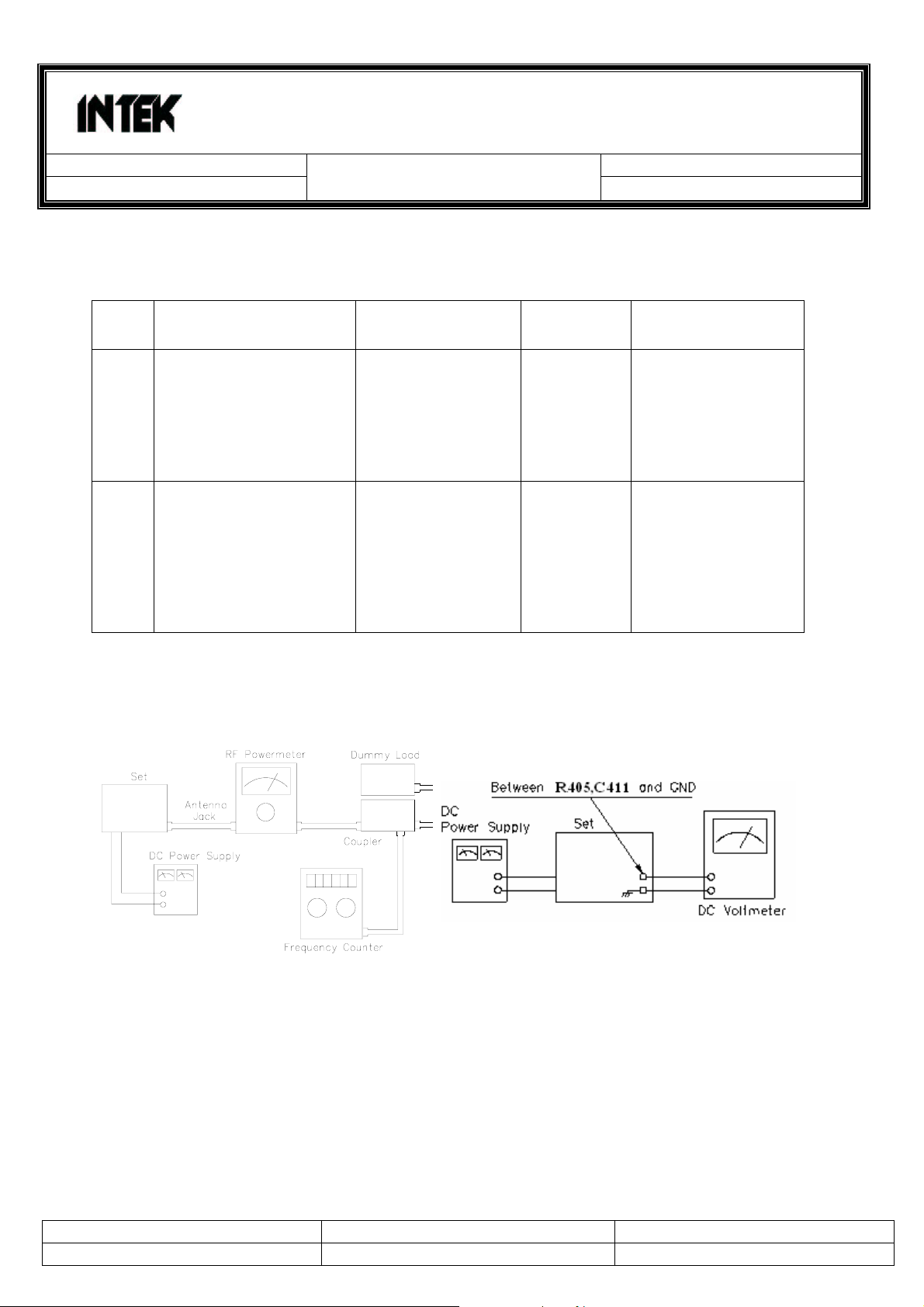
Frequency counter
to dummy load
(Figure 1).
Connect DC
voltmeter between
R406, C411 and
GND.
(Figure 2).
CT201
L501 1V at TX.
27.185MHz±300Hz
Figure 1 Figure 2
Created by: Approved by: Rev.No:
For Stage: Release Date: Page: 8 / 60
Model No: 3391 Drawring No:
Customer :
Model No:
M-790 Plus
Rev,Date:
TRANSMITTER SECTION
Test Equipment Required
• RF power meter (RF SSVM) • DC power supply (13.2 volt, 3 amp)
• 50 ohms dummy load (non-inductive) • Spectrum analyzer
• RF attenuator (50 ohms non-inductive) • Frequency counter
• Oscilloscope • Coupler
• Audio generator
ALIGNMENT PROCEDURE
Step Setting
RF power stage
MIC : Transmit
Volume : optional
Squelch : optional
1
CH : selector : 19
CH9 : OFF
Second harmonic
check
MIC : Transmit
Volume : optional
Squelch : optional
CH : selector : 19
CH9 : OFF
2
Connection Adjuster Adjust for
Connect dummy load
and RF power meter to
the EXT-ANT jack on the
set (Figure 3).
Connect RF power meter
With dummy load to
spectrum analyzer
through coupler /-40 dB
Attenuator to EXT-ANT
jack on the set
(Figure 4).
L301
L302
L303
At no modulation,
Maximum indication
on the power meter (4
watts). If indication is
not in 4 watts range,
adjust L301, L302,
L303.
compare the level o
fundamental
frequency to the level
of harmonic
frequency.
Suppression of the
nd
2
harmonic
frequency level must
be lower than –60 dB.
Check for the other
channels.
Frequency check
MIC : Transmit
Volume : optional
Squelch : optional
3
CH : selector : 19
CH9 : OFF
Connect dummy load
and frequency counter
though coupler to RF
powermeter. Connect RF
powermeter to EXT-ANT
jack on the set
(Figure 5).
CT201 Be sure that the
indication of the
transmitter frequency
is 27.185MHz±300Hz
on the frequency
counter.
Created by: Approved by: Rev.No:
For Stage: Release Date: Page: 9 / 60

Model No: 3391 Drawring No:
Customer :
Model No:
M-790 Plus
Rev,Date:
TX power level
adjustment
Volume : optional
Squelch : optional
4
CH : selector : 1
CH9 : OFF
Connect dummy load
and oscilloscope through
Coupler to RF
powermeter connect
audio generator to
microphone jack
(Figure 6).
RV202 Adjust until the 5
appears on the
channel display LCD.
th
bar
Figure 3
Created by: Approved by: Rev.No:
For Stage: Release Date: Page: 10 / 60

Model No: 3391 Drawring No:
Customer :
Model No:
M-790 Plus
Rev,Date:
Figure 4
RECEIVER SECTION
Test Equipment Required
• RF Signal generator (RFSG)
• SSVM
• Distortion meter
• DC power supply
ALIGNMENT PROCEDURE
Step Setting
Audio output adjustment
MIC : Receive
Volume : Fully clockwise
Squelch: Turn to-
Counter clockwise
CH selector : 19
RF gain : Fully clockwise
1
CH9 : OFF
RFSG:27.185 MHz,1kHZ
1µV , 1.2 K Dev.
Connect RF signal
generator to EXT-ANT
jack. Connect SSVM
and distortion meter
with 8 ohm dummy
load
(Figure 7).
Connection Adjuster Adjust for
L101
L102
L103
L104
L106
L401
L402
L403
Maximum indication
on SSVM. Reduce
output from RFSG
until the audio output
becomes about
500mW (2V).
Created by: Approved by: Rev.No:
For Stage: Release Date: Page: 11 / 60
Model No: 3391 Drawring No:
Customer :
Model No:
M-790 Plus
Rev,Date:
Squelch adjustment
MIC : Receive
Volume : 50mW (2V)
Squelch : Clockwise
2
CH selector : 19
RFSG:27.185MHz, 1kHZ
1mV, 1.2K DEV.
Connect RF signal
generator to EXT-ANT
Jack. Connect SSVM
and distortion meter to
EXT speaker jack with
8 ohm dummy load
(Figure 7).
RV1 Adjust until the audio
output appears.
RF signal meter adjustment
MIC : Receive
Volume : 500mW (2V)
Squelch : Fully counter
3
Clockwise
RFSG: 27.185 MHz, 1kHZ,
1µV, 1.2K Dev.
Connect RF signal
generator to EXT-ANT
Jack. Connect SSVM
and distortion meter to
EXT speaker jack with
8 ohm dummy load
(Figure 7).
RV101 Adjust until the 3
LED on the S/RF
meter lights up.
rd
Figure 5
Created by: Approved by: Rev.No:
For Stage: Release Date: Page: 12 / 60
Model No: 3391 Drawring No:
Customer :
Model No:
M-790 Plus
Rev,Date:
Figure 6
Figure 7
Created by: Approved by: Rev.No:
For Stage: Release Date: Page: 13 / 60
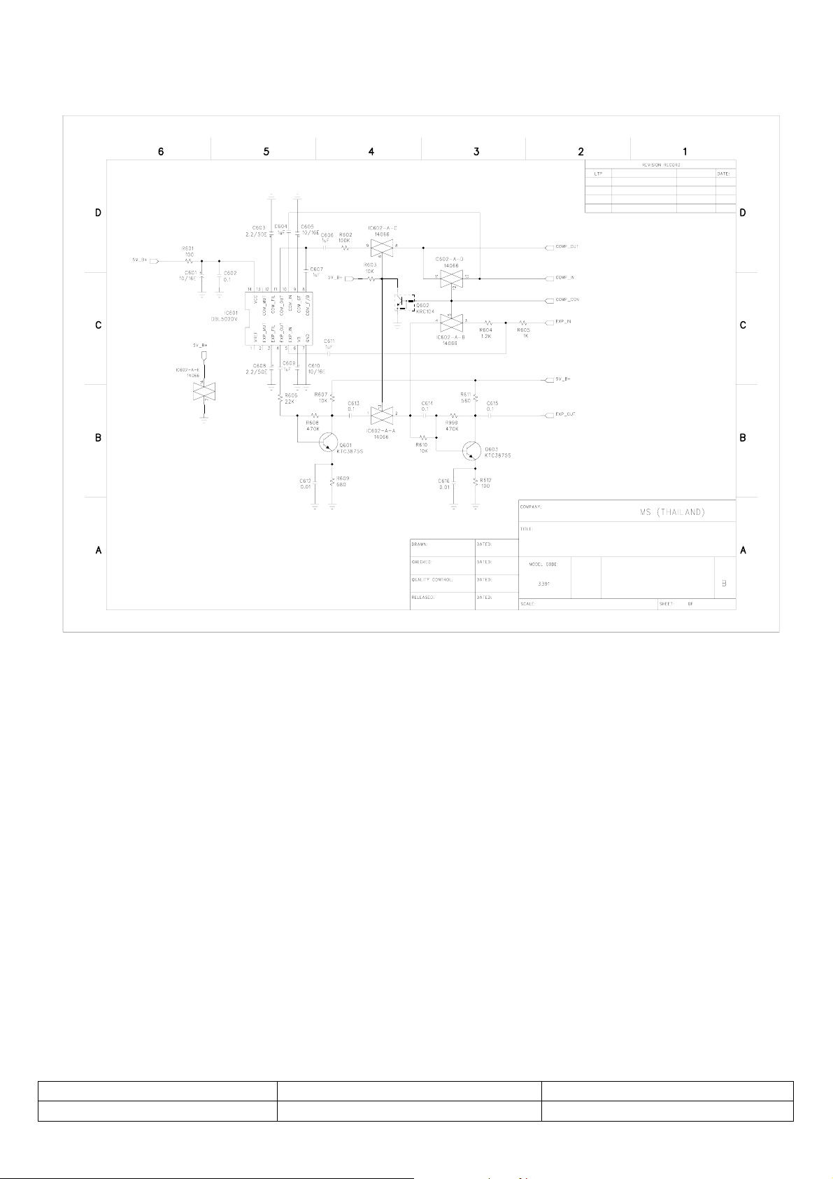
INTEK M-790 ESP
Created by: Approved by: Rev.No:
For Stage: Release Date: Page: 16 / 60
Model No: 3391 Drawring No:
Customer :
Model No:
M-790 Plus
Rev,Date:
PLL CIRCUIT BLOCK DIAGRAM
1. INTRODUCTION
The frequencies for transmitter and receiver first local frequencies are all derived from a single 4.5 MHz
crystal by means of a phase locked loop. The first local oscillator frequencies are 16.270 MHz (CH 1) to
16.710 MHz (CH 40) for EU and 16.90625 MHz (CH 1) to 17.29625 MHz (CH 40) for UK . The second
local frequency is fixed at 10.240 MHz to generate second IF 455 KHz. During transmit, The VCO of
the PLL operates 13.4825 MHz (CH 1) to 13.7025 MHz (CH 40) for EU ,13.800625 MHz (CH 1) to
13.995625 MHz (CH 40) for UK the VCO frequency gose to the double circuit Q301,L301,L302 which
doubles the frequency to generate 26.965 MHz (CH 1) to 27.405 MHz (CH 40) for EU and 27.60125
MHz (CH 1) to 27.99125 MHz (CH 40) for UK
13.4825 MHz (CH 1) EU 26.965 MHz (CH 1)
13.7025 MHz (CH 40) EU 27.405 MHz (CH 40)
13.800625 MHz (CH 1) UK 27.60125 MHz (CH 1)
13.995625 MHz (CH 40) UK 27.99125 MHz (CH 40)
The VCO operating frequency for the receiver is 16.270,16.90625 MHz (CH 1) to 16.710,17.29625 MHz
(CH 40) as the first local oscillator, injected through the buffer AMP Q506 into the first fed balanced
mixer Q107,Q108
Q 408
VCO
Q 301
Doubler
To Transmitter
Created by: Approved by: Rev.No:
For Stage: Release Date: Page: 17 / 60
Model No: 3391 Drawring No:
Customer :
Model No:
M-790 Plus
Rev,Date:
2. BASIC SYNTHESIZER SCHEME
The crystal frequency (4.500 MHz) is divided by 1800 times to make 2.5 KHz which is fed to one side of
the phase detector. The VCO output is divided by a programmable divider, and fed to other side of the
phase detector Pin 75 of IC101. The feedback loop is closed by passing the phase detector output
through an active low pass filter and using the output to control the VCO frequency through varicap
diode D503,D504
Under locked conditions, both of phase detector input signal must be indential at 2.5 KHz. The VCO
frequency is then given by:
FVCO / N = 0.0025 MHz or FVCO = 0.0025 x N MHz
Since “N” is an integer, the VCO frequency can be stepped up with 2.5 KHz increments. By suitable
choice of “N” the desired output frequency can be obtained.
Channel 1 Channel 40
Function
N FVCO N FVCO
Transmit 5393 13.4825 5481 13.7025
EU
Receive 6508 16.2700 6684 16.7100
Transmit 5520.25 13.800625 5598.25 13.995625
UK
Receive 6762.50 16.90625 6918.5 17.29625
(SEE TABLE FOR OTHER CHANNELS)
Created by: Approved by: Rev.No:
For Stage: Release Date: Page: 18 / 60
Model No: 3391 Drawring No:
Customer :
The VCO frequency goes to the double circuit, which doubles the incoming signals.
Model No:
M-790 Plus
Rev,Date:
Double output Frequency
Transmit
_______
Transmit
_______
Since all frequencies are obtained from the crystal controlled PLL oscillator, all outputs are coherent
with the crystal oscillator frequency and maintaining the same percentage accuracy.
CH 1, 13.4825 MHz
CH 1, 13.800625 MHz
CH 40, 13.7025 MHz
CH 40, 13.995625 MHz
26.965 MHz
27.60125 MHz
27.405 MHz
27.99125 MHz
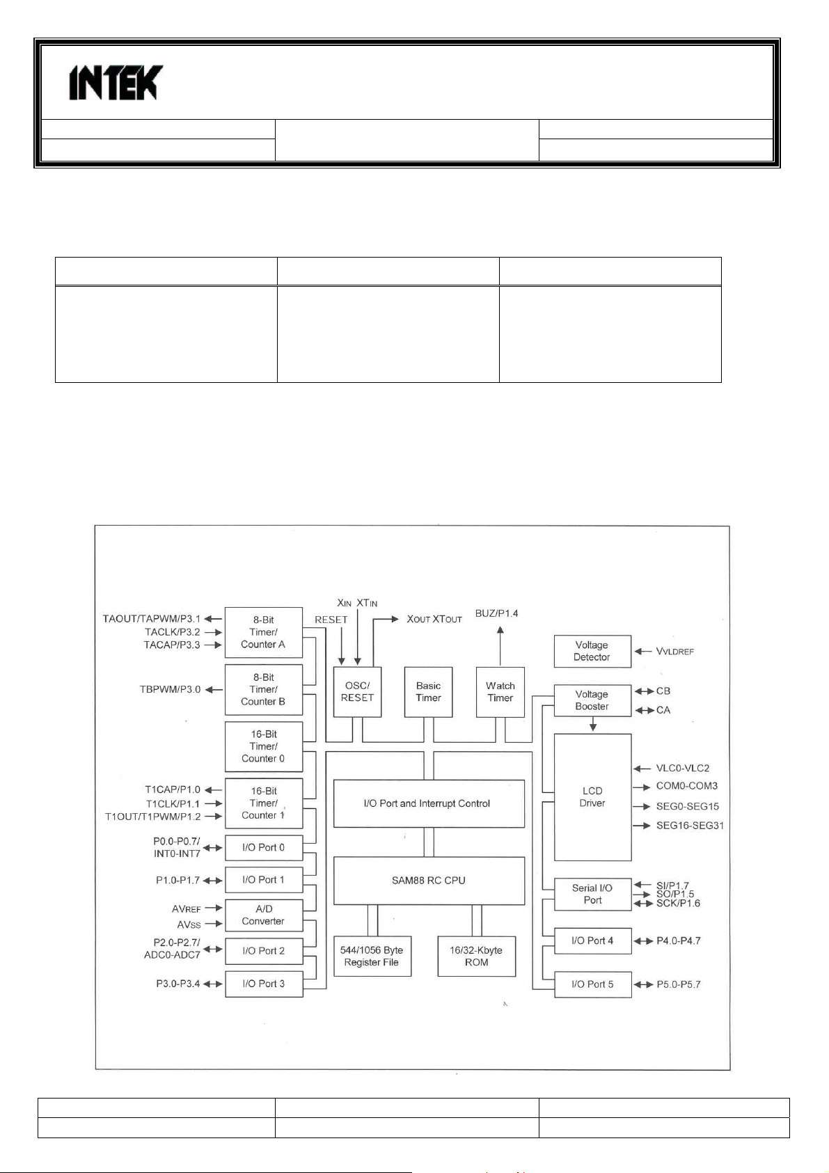
INTERNAL BLOCK DIAGRAM
Created by: Approved by: Rev.No:
For Stage: Release Date: Page: 19 / 60
Model No: 3391 Drawring No:
Customer :
DIVIDE RATIO, VCO RX/TX FREQUENCIES FOR EACH CHANNEL OF “EU”
Model No:
M-790 Plus
Rev,Date:
Channels
1 26.965 6508 16.27 5393 13.4825
2 26.975 6512 16.28 5395 13.4875
3 26.985 6516 16.29 5397 13.4925
4 27.005 6524 16.31 5401 13.5025
5 27.015 6528 16.32 5403 13.5075
6 27.025 6532 16.33 5405 13.5125
7 27.035 6536 16.34 5407 13.5175
8 27.055 6544 16.36 5411 13.5275
9 27.065 6548 16.37 5413 13.5325
10 27.075 6552 16.38 5415 13.5375
11 27.085 6505 16.39 5417 13.5425
12 27.105 6512 16.41 5421 13.5525
13 27.115 6516 16.42 5423 13.5575
14 27.125 6524 16.43 5425 13.5626
15 27.135 6528 16.44 5427 13.5675
16 27.155 6532 16.46 5431 13.5775
17 27.165 6536 16.47 5433 13.5825
18 27.175 6544 16.48 5435 13.5875
19 27.185 6548 16.49 5437 13.5925
20 27.205 6552 16.51 5441 13.6025
21 27.215 6608 16.52 5443 13.6075
22 27.225 6612 16.53 5445 13.6125
23 27.255 6624 16.56 5451 13.6275
24 27.235 6616 16.54 5447 13.6175
25 27.245 6620 16.55 5449 13.6225
26 27.265 6628 16.57 5453 13.6325
27 27.275 6632 16.58 5455 13.6375
28 27.285 6636 16.59 5457 14.6425
29 27.295 6640 16.60 5459 13.6475
30 27.305 6644 16.61 5461 13.6525
31 27.315 6648 16.62 5463 13.6575
32 27.325 6652 16.63 5465 13.6625
33 27.335 6656 16.64 5467 13.6675
34 27.345 6660 16.65 5469 13.6725
35 27.355 6664 16.66 5471 13.6775
36 27.365 6668 16.67 5473 13.6825
Frequencies
(MHz)
RX TX
Frequencies MHz
Frequencies MHz
Created by: Approved by: Rev.No:
For Stage: Release Date: Page: 20 / 60

Model No: 3391 Drawring No:
Customer :
Model No:
M-790 Plus
Rev,Date:
37 27.375 6672 16.68 5475 13.6875
38 27.385 6676 16.69 5477 13.6925
39 27.395 6680 16.70 5479 13.6975
40 27.405 6684 16.71 5481 13.7025
DIVIDE RATIO, VCO RX/TX FREQUENCIES FOR EACH CHA NNEL OF “UK”
Channels
1 27.60125 6546.5 16.90625 5412.25 13.800625
2 27.61125 6766.5 16.91625 5522.25 13.805625
3 27.62125 6770.5 16.92625 5524.25 13.810625
4 27.63125 6774.5 16.93625 5526.25 13.815625
5 27.64125 6778.5 16.94625 5528.25 13.820625
6 27.65125 6782.5 16.95625 5530.25 13.825625
7 27.66125 6786.5 16.96625 5532.25 13.830625
8 27.67125 6790.5 16.67625 5534.25 13.835625
9 27.68125 6794.5 16.98625 5536.25 13.840625
10 27.69125 6798.5 16.99625 5538.25 13.845625
11 27.70125 6802.5 17.00625 5540.25 13.850625
12 27.71125 6806.5 17.01625 5542.25 13.855625
13 27.72125 6810.5 17.02625 5544.25 13.860625
14 27.73125 6814.5 17.03625 5546.25 13.865625
15 27.74125 6818.5 17.04625 5548.25 13.870625
16 27.75125 6822.5 17.05625 5550.25 13.875625
17 27.76125 6826.5 17.06625 5552.25 13.880625
18 27.77125 6830.5 17.07625 5554.25 13.885625
19 27.78125 6834.5 17.08625 5556.25 13.890625
20 27.79125 6838.5 17.09625 5558.25 13.895625
21 27.80125 6842.5 17.10625 5560.25 13.900625
22 27.81125 6846.5 17.11625 5562.25 13.905625
23 27.82125 6850.5 17.12625 5564.25 13.910625
24 27.83125 6854.5 17.13625 5566.25 13.915625
25 27.84125 6858.5 17.14625 5568.25 13.920625
26 27.85125 6861.5 17.15625 5570.25 13.925625
27 27.86125 6866.5 17.16625 5572.25 13.930625
28 27.87125 6870.5 17.17625 5574.25 13.935625
29 27.88125 6874.5 17.18625 5576.25 13.940625
30 27.89125 6878.5 17.19625 5578.25 13.945625
Frequencies
(MHz)
RX TX
Frequencies MHz
Frequencies MHz
Created by: Approved by: Rev.No:
For Stage: Release Date: Page: 21 / 60
 Loading...