

现货库存、技术资料、百科信息、热点资讯,精彩尽在鼎好!
Multi-Voltage Processor Power Supply
Data Sheet
1Overview
1.1 Features
• High efficiency regulator system
• Wide input voltage range from 5.5V to 60V
• Stand-by mode with low current consumption
• Suitable for standard 12V/24V and 42V PowerNets
• Step down converter as pre-regulator:
5.5V / 1.5A
• Step down slope control for lowest EME
• Switching loss minimization
• Three high current linear post-regulators with
selectable output voltages:
5V / 800mA
3.3V or 2.6V / 500mA
3.3V or 2.6V / 350mA
• Six independent voltage trackers (followers):
5V / 17mA each
• Stand-by regulator with 1mA current capability
• Three independent undervoltage detection circuits
(e.g. reset, early warning) for each linear post-regulator
• Power on reset functionality
• Tracker control and diagnosis by SPI
• All outputs protected against short-circuit
• Power-DSO-36 package
TLE 6368 / SONIC
P-DSO-36-12
Type Ordering Code Package
TLE 6368 G1 / SONIC Q67007-A9648 P-DSO-36-12
SMD = Surface Mounted Device
Data Sheet, Rev. 1.32 1 2004-10-15

TLE 6368 / SONIC
1.2 Short functional description
The
TLE 6368 G1 / SONIC is a multi voltage power supply system especially designed
for automotive applic ations usi ng a standa rd 12V / 24V batte ry as well as the new 42V
powernet. The device is intended to supply 32 bit micro-controller systems which require
different supply voltage rails such as 5V, 3.3V and 2.6V. The regulators for external
sensors are also provided.
The TLE 6368 G1 / SONIC cascades a Buck converter block with a linear regulator and
tracker block on a single chip to achieve lowest power dissipation thus being able to
power the application even at very high ambient temperatures.
The step-down converter delivers a pre-regulated voltage of 5.5V with a minimum
current capability of 1.5A.
Supplied by this step down converter three low drop linear post-regulators offer 5V, 3.3V,
or 2.6V of output voltages dependi ng on the configuration of the device with current
capabilities of 800mA, 500mA and 350mA.
In addition the inputs of six voltage trackers are connected to the 5.5V bus voltage. Their
outputs follow the main 5V linear regulator (Q_LDO1) with high accuracy and are able to
drive a current of 17mA each. The trackers can be turned on and off individually by a 16
bit serial peripheral interfac e (SPI). Throu gh t his inte rf ace als o the stat us i nform atio n of
each tracker (i.e. short circuit) can be read out.
To monitor the outp ut voltage le vels of each of the linear reg ulators three i ndependent
undervoltage detection circui ts are ava ila ble w hic h can be us ed to impl eme nt the reset
or an early warning function. The supervision of the µC can be managed by the SPItriggered window watchdog.
For energy saving reasons while the motor is turned off, the TLE 6368 G1 / SONIC offers
a stand-by mode, where the qu iescent current does n ot exceed 30µA. In this stand -by
mode just the stand-by regulator remains active.
The TLE 6368 G1 / SONIC is based on Infineon Power technology SPT which allows
bipolar , CMOS and Power DMOS circuitry to be integrated on the same monolithic
circuitry.
Data Sheet, Rev. 1.32 2 2004-10-15
1.3 Pin configuration
TLE 6368 / SONIC
P-DSO-36-12
GND
CLK
CS
DO
ERR
Q_STB
Q_T1
Q_T2
Q_T3
Q_T4
DI
1
2
3
4
5
6
7
8
9
10
11
TLE 6368
36
35
34
33
32
31
30
29
28
27
26
GND
SLEW
WAKE
BOOST
IN
SW
IN
SW
Bootstrap
Q_LDO1
FB/L_IN
Q_T5
Q_T6
Q_LDO3
R3
R2
R1
GND
12
13
14
15
16
17
18
25
24
23
22
21
20
19
FB/L_IN
Q_LDO2
SEL
CCP
C+
C-
GND
Figure 1 Pin Configuration (Top View),
bottom heat slug and GND corner pins are connected
Data Sheet, Rev. 1.32 3 2004-10-15
TLE 6368 / SONIC
rcuit Information
1.4 Pin definitions and functions
Pin No. Symbol Function
1,18,19,36GND Ground; to reduce thermal resistance place cooling areas on
PCB close to these pins. The GND pins are connected internally
to the heat slug at the bottom.
2CLKSPI Interface Clock input; clocks the shift register; CLK has an
internal active pull down and requires CMOS logic level
inputs;see also chapter SPI
3CS
SPI Interface chip select input; CS is an active low input; serial
communication is enabled by pulling the CS
input should only be switched when CLK is low; CS
terminal low; CS
has an
internal active pull up and requires CMOS logic level inputs ;see
also chapter SPI
4DI SPI Interface Data input; receives serial data from the control
device; serial data transmitted to DI is a 16 bit control word with
the Least Significant Bit (LSB) being transferred first; the input
has an active pull down and requires CMOS logic level inputs; DI
will accept data on the falling edge of CLK-signal; see also
chapter SPI
5DOSPI Interface Data output; this tristate output transfers
diagnosis data to the controlling device; the output will remain 3stated unless the device is selected by a low on Chip-Select CS
see also the chapter SPI
6ERR
Error output; push-pull output. Monitors failures in parallel to the
SPI diagnosis word, reset via SPI. ERR
is an active low, latched
output.
;
7Q_STBStandby Regulator Output; the output is active even when the
buck regulator and all other circuitry is in off mode
8 Q_T1 Voltage Tracker Output T1 tracked to Q_LDO1; bypass with a
1µF ceramic capacitor for stability. It is switched on and off by
SPI command. Keep open, if not needed.
9 Q_T2 Voltage Tracker Output T2 tracked to Q_LDO1; bypass with a
1µF ceramic capacitor for stability. It is switched on and off by
SPI command. Keep open, if not needed.
10 Q_T3 Voltage Tracker Output T3 tracked to Q_LDO1; bypass with a
1µF ceramic capacitor for stability. It is switched on and off by
SPI command. Keep open, if not needed.
Data Sheet, Rev. 1.32 4 2004-10-15
TLE 6368 / SONIC
1.4 Pin definitions and functions (cont’d)
Pin No. Symbol Function
11 Q_T4 Voltage Tracker Output T4 tracked to Q_LDO1; bypass with a
1µF ceramic capacitor for stability. It is switched on and off by
SPI command. Keep open, if not needed.
12 Q_T5 Voltage Tracker Output T5 tracked to Q_LDO1; bypass with a
1µF ceramic capacitor for stability. It is switched on and off by
SPI command. Keep open, if not needed.
13 Q_T6 Voltage Tracker Output T6 tracked to Q_LDO1; bypass with a
1µF ceramic capacitor for stability. It is switched on and off by
SPI command. Keep open, if not needed.
14 Q_LDO3 Voltage Regulator Output 3; 3.3V or 2.6V output; output
voltage is selected by pin SEL (see also 2.2.2); For stability a
ceramic capacitor of 470nF to GND is sufficient.
15 R3 Reset output 3, undervoltage detection for output Q_LDO3;
open drain output; an external pullup resistor of 10kΩ is
required
16 R2 Reset output 2, undervoltage detection for output Q_LDO2;
open drain output; an external pullup resistor of 10kΩ is
required
17 R1 Reset output 1, undervoltage detection for output Q_LDO1 and
watchdog failure reset; open drain output ; an external pullup
resistor of 10kΩ is required
20 C- Charge pump capacitor connection; Add the fly-capacitor of
100nF between C+ and C-
21 C+ Charge pump capacitor connection; Add the fly-capacitor of
100nF between C+ and C-
22 CCP Charge Pump Storage Capacitor Output; Add the storage
capacitor of 220nF between pin CCP and GND.
23 SEL Select Pin for output voltage adjust of Q_LDO2 and Q_LDO3
(see also 2.2.2)
24 Q_LDO2 Voltage Regulator Output 2; 3.3V or 2.6V output; output
voltage is selected by pin SEL (see also 2.2.2); For stability a
ceramic capacitor of 470nF to GND is sufficient.
25, 26 FB/L_IN Feedback and Linear Regulator Input; input connection for
the Buck converter output
Data Sheet, Rev. 1.32 5 2004-10-15
TLE 6368 / SONIC
1.4 Pin definitions and functions (cont’d)
Pin No. Symbol Function
27 Q_LDO1 Voltage Regulator Output 1; 5V output; acts as the reference
for the voltage trackers.The SPI and window watchdog logic is
supplied from this voltage. For stability a ceramic capacitor of
470nF to GND is sufficient.
28 Bootstrap Bootstrap Input; add the bootstrap capacitor between pin SW
and pin Bootstrap, the capcitance value should be 2% of the
Buck converter output capacitance
29, 31 SW Switch Output; connect both pins externally through short lines
directly to the cathode of the catch diode and the Buck circuit
inductance.
30, 32 IN Supply Voltage Input; connect both pins externally through
short lines to the input filter/the input capacitors.
33 BOOST Boost Input; for switching loss minimization connect a diode
(cathode directly to boost pin) in series with a 100nF ceramic
capacitor to the IN pin and from the anode of the diode to the
buck converter output a 22Ω resistor. Recommended for 42V
applications. In 12/24V applications connect boost directly to IN.
34 WAKE Wake Up Input; a positive voltage applied to this pin turns on
the device
35 SLEW Slew control Input; a resistor to GND defines the current slope
in the buck switch for reduced EME
Data Sheet, Rev. 1.32 6 2004-10-15
1.5 Basic block diagram
Boost
IN
2*
Slew
OSZ PWM
Driver
TLE 6368
Standby
Regulator
REGULATOR
Error-
Amplifier
feedback
BUCK
Internal
Reference
Q_STB
SW
Bootstrap
FB/L_IN
TLE 6368 / SONIC
2*
2*
Wake
R1
R2
R3
CLK
CS
DI
DO
ERR
Protection
Power
Down
Logic
Reset
Logic
Window
Watchdog
SPI
16 bit
C+
CCP
SEL
Q_LDO1
Q_LDO2
Q_LDO3
Q_T1
Q_T2
Q_T3
Q_T4
Q_T5
Q_T6
C-
µ-controller /
memory
supply
Sensor
supplies
(off board
supplies)
Charge
Pump
Linear
Reg. 1
Linear
Reg. 2
Linear
Reg. 3
ref
Tracker
5V
ref
Tracker
5V
ref
Tracker
5V
ref
Tracker
5V
ref
Tracker
5V
ref
Tracker
5V
GND
4*
Figure 2 Block Diagram
Data Sheet, Rev. 1.32 7 2004-10-15
TLE 6368 / SONIC
2 Detailed circuit description
In the following major buck regulator b locks, the linear vo ltage regul ators and track ers,
the undervoltage reset function, the watchdog and the SPI are described in more detail.
For applications information e.g. choice of external components, please refer to section
5.
2.1 Buck Regulator
The diagram below shows the internal implemented circuit of the Buck converter, i. e. the
internal DMOS devices, the regulation loop and the other major blocks.
5V 14V
Int. volta ge
regulator
FB/L_IN
C+
C-
Divider
Oscillator
1.4MHz
Voltage
feedback
amplifier
Vref=6V
from
current sensing
Current
sense
amplifier
+
Lowpass
Lowpass
8 to 10V
CCP
Int. charge
pump
150µA
Slope
compensation
Current
comparator
BOOTSTRAP
switchi ng frequency 330kHz
Gate off signal
fr om overtem p or
sleep command
Trigger for
gate off
Trigger for
gate on
PWM logic
Main switch ON/OFF
SW
Slope logi c
Delay unit
Gate driver
Slope switc h
charge signal
Slope switch
discharg e sign al
undervoltage
lockout
Zero cross
detection
to
current sense
amplifi er
Main
DMOS
Slope
DMOS
IN
IN
BOOST
SW
Slope
control
SLEW
exter nal comp onents
pins
Figure 3 Detailed Buck regulator diagram
The 1.5A Buck regulator consists of two internal DMOS power stages including a current
mode regulation scheme to avoid external compensation components plus additional
blocks for low EME and reduced switching loss. Figure 3 indicates also the principle how
Data Sheet, Rev. 1.32 8 2004-10-15

TLE 6368 / SONIC
the gate driver supply is managed by the combination of internal charge pump, external
charge pump and bootstrap capacitor.
2.1.1 Current mode control scheme
The regulation loop is located at the left lower corner in the schematic, there you find the
voltage feedback amplifier which gives the actual information of the actual output voltage
level and the current sense ampl ifier for the load current inform ation to form finally the
regulation signal. To avoid subh armo nic osci llations at duty cycles highe r than 5 0% the
slope compensation block is necessary.
The control signal formed out of those three blocks is finally the input of the PWM
regulator for the DMOS gate turn off command, which means this signal determines the
duty cycle. The gate turn on signal is set by the o scillator periodical ly every 3µs which
leads to a Buck converter switching frequency around 330kHz.
With decreasing input voltag e the de vic e ch anges to the so called pulse skipp ing mode
which means basically that some of the oscillator gate turn off signals are ignored. When
the input voltage is still reduced the DMOS is turned on statically (100% duty cycle) and
its gate is supplied by the internal charge pump. Below typic al 4. 5V at the feedback pin
the device is turned off.During normal switching operation the gate driver is supplied by
the bootstrap capacitor.
2.1.2 Start-up procedure
To guarantee a device startup even under full load condition at the linear regulator
outputs a special start up procedure is impleme nted. At first the bootstrap capa citor is
charged by the internal charge pump. Afterwards the output capacitor is charged where
the driver supply in tha t case is maintained only by the bootstrap capacitor. Once the
output capacitor of the buck converter is charged the external charge pump is activated
being able to supply the linear regulators and finally the linear regulators are released to
supply the loads.
2.1.3 Reduction of electromagnetic emission
In figure 3 it is recognized that two internal DMOS switches are used, a main switch and
an auxiliary switch. The second imp lemented switc h is used to adjust the current slope
of the switching current. The slope adjustment is done by a controlled charge and
discharge of the gate of this DMOS. By choosi ng the external resistor on the SLEW pin
appropriate the current transition time can be adjusted between 20ns and 100ns.
2.1.4 Reducing the switching losses
The second purpose of the slope DMOS is to minimise the switching losses. Once being
in freewheeling mode of the buck regulato r the output volta ge level is sufficient to force
the load current to flow, the in put voltage level is not needed in the first mo ment. By a
feedback network consis ting of a resistor and a diode to th e boost pin (connectio n see
Data Sheet, Rev. 1.32 9 2004-10-15

TLE 6368 / SONIC
section 5) the output voltage level is pres ent at the drain of the switch. As soon as the
voltage at the SW pin passes zero volts the handover to the main switch occurs and the
traditional switching behaviour of the Buck switch can be observed.
2.2 Linear Voltage Regulators
The Linear regulators offer, depending on the version, voltage rails of 5V, 3.3V and 2.6V
which can be determined by a hardware connection (see table at 2.2.2) for proper power
up procedure. Being supplied by the output of the Buck pre-regulator the power loss
within the three linear regulators is minimized.
All voltage regulators are short circuit protected which means that each regulator
provides a maximum cu rrent according to its current li mit when shorted. Together with
the external charge p ump the NPN pass elemen ts of the regulators allow low dropout
voltage operation. By u sing this structu re the linear regulat ors work stable even with a
minimum of 470nF ceramic capacitors at their output.
Q_LDO1 has 5V nominal output voltage, Q_LDO2 has a hardware programmable
output voltage of 3.3V or 2.6V and Q_LDO3 is also programmable to 3.3V or 2.6V (see
section 2.2.2). All th ree regulators are on all the time, i f one regulator is n ot needed a
base load resistor in parallel to the output capacitance for controlled power down is
recommended.
2.2.1 Startup Sequence Linear Regulators
When acting as a 32 bi t µC s uppl y the so-called power seque nci ng (the dependency of
the different voltage rails to each other) is important. Within the TLE 6368 G1 / SONIC,
the following Startup-Sequence is defined (see also figure 4):
V
Q_LDO2
with V
≤ V
Q_LDO1
Q_LDO1; VQ_LDO3
=5V, V
Q_LDO2
≤ V
Q_LDO1
= 2.6V or 3.3V and V
Q_LDO3
= 2.6V or 3.3V
The power sequencing refers to the regulator itself, externally voltages applied at
Q_LDO2 and Q_LDO3 are not pulled down actively by the device if Q_LDO1 is lower
than those outputs.
That means for the power down se quencing if different output capa citors and different
loads at the three outputs of the linear regulators are used the voltages at Q_LDO2 and
Q_LDO3 might be higher than at Q_LDO1 due to slower discharging. To avoid this
behaviour three Schottky diodes have to be connected between the three outputs of the
linear regulators in that way that the cathodes of the diodes are always connected to the
higher nominal rail.
Data Sheet, Rev. 1.32 10 2004-10-15
Power Sequencing
V
FB/L_IN
V
LDO_EN
V
Q_LDO1
5V
V
Rth5
3.3V
2.6V
V
(2.6V Mode)
Q_LDO2
TLE 6368 / SONIC
t
t
0.7V
5V LDO 5V LDO
5V LDO 5V LDO
+/- 50mV
0.7V
t
+/- 50mV
t
V
Q_LDO3
2.6V
V
3.3V
V
Rth2.6
Rth3.3
(3.3V Mode)
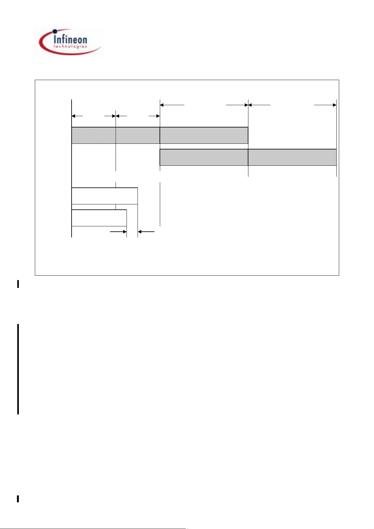
Figure 4 Power-up and -down sequencing of the regulators
2.2.2 Q_LDO2 and Q_LDO3 output voltage selection*
To determine the output voltage le vels of the three linear regulators, the se lection pin
(SEL, pin 23) has to be connected according to the matrix given in the table below.
Definition of Output voltage Q_LDO2 and Q_LDO3
Select Pin SEL
connected to
Q_LDO2
output voltage
Q_LDO3
output voltage
GND 3.3 V 3.3 V
Q_LDO1 2.6 V 2.6 V
Q_LDO2 2.6 V 3.3 V
* for different output voltages ple as e ref er t o th e m ult i vo lta ge s upply TLE6361
Data Sheet, Rev. 1.32 11 2004-10-15

TLE 6368 / SONIC
2.3 Voltage Trackers
For off board supplies i.e. sensors six voltage trackers Q_T1 to Q_T6 with 17mA output
current capability each are available. The output voltages match Q_LDO1 within
+5 / -15mV. They can be individually turned on and off by the appropriate SPI command
word sent by the microcontroller. A ceramic capacitor with the value of 1µF at the output
of each tracker is sufficient for stable operation without oscillation.
The tracker outputs can be connected in parallel to obtain a higher output current
capability, no matter if on ly two or up to all si x trackers are tied together. For uniform ly
distributed current d ensity in eac h tracker interna l balance res istors at each output are
foreseen internally. By connecting two sets of three trackers in parallel two sensors with
more than 50mA each can be supplied, all six in parallel give more than 100mA.
The tracker outputs can withstand short circuits to GND or battery in a range from -5 to
+60V. A short circuit to GND is detected and indicated individually for each tracker in the
SPI status word. Also a n open load condi tion might be recognised a nd indicated as a
failure condition in the SPI status word. A minimum load current of 2mA is required to
avoid open load failure indica tion. In cas e of connecti ng several tra ckers to a comm on
branch balancing currents can prevent proper operation of the failure indication.
2.4 Standby Regulator
The standby regulator is an ultra low power 2.5V linear voltage regulator with 1mA output
current which is on all the time. It is intended to supply the mic r oco ntrol ler in stop mode
and requires then onl y a minimum of quiescent current (<3 0µA) to extend the battery
lifetime.
2.5 Charge Pump
The 1.6 MHz charge pump with the two external capacitors will serve to supply the base
of the NPN linear regulators Q_LDO1 and Q_LDO3 as well as the gate of the Buck
DMOS transistor in 100% duty cycle operation at low battery condition. The charge pump
voltage in the range of 8 to 10V can be measured at pin 22 (CCP) but is not intended to
be used as a supply for additional circuitry.
2.6 Power On Reset
A power on reset is available for eac h linear voltage regu lator output. The reset out put
lines R1, R2 and R3 ar e ac tiv e (lo w) d uring sta rt up a nd turn inactive with a rese t delay
time after Q_LDO1, Q_LDO2 and Q_LDO3 have reached their reset threshold. The
reset outputs are open drain, three pull up resistors of 10kΩ each have to be co nne ct e d
to the I/O rail (e.g. Q_LDO1) of the µC. All three reset outputs can be linked in parallel to
obtain a wire d-OR.
The reset delay time is 8 ms by default and can be set to higher values as 16 ms, 32 ms
or 64 ms by SPI command. At each power up of the device in case the output voltage at
Data Sheet, Rev. 1.32 12 2004-10-15
TLE 6368 / SONIC
Q_LDO1 had decreased below 3.3V (max.), the SPI will reset to the default settings
including the 8ms delay time. If the voltage on Q_LDO1 during sleep or power off mode
was kept above 3.3V the delay time set by the last SPI command is valid.
V
FB/L_IN
V
Q_LDOx
< t
rr
t
rr
V
Rx
t
RES
t
RES
t
RES
t
RES
t
V
RTH,Q_LDOx
t
t
thermal
shutdown
under
voltage
over
load
Figure 5 Undervoltage reset timing
2.7 RAM good flag
A RAM good flag will be set within the SPI status word when the Q_LDO1 voltage drops
below 2.3V. A second one wi ll be set if Q_LDO2 drops belo w typical 1.4V. Both RAM
good flags can be read after power up to determine if a c old or warm start n eeds to be
processed. Both RAM good flags will be reset after each SPI cycle.
2.8 ERR
Pin
A hardware error pin indicates any fault conditions on the chip. It should be connected to
an interrupt input of the microcontroller. A low signa l indicates an error condition. The
microcontroller can read the root cause of the error by reading the SPI register.
2.9 Window Watchdog
The on board window watchdog for supervision of the µC works in combination with the
SPI. The window watchdog logic is turned off per default and can be activated by one
special bit combination in the SPI command word. When operating, the window
watchdog is triggered when CS is low and Bit WD-Trig in the SPI command word is set
to “1”. The watchdog trigger is recognized with the low to high transition of the CS
signal.
To allow reading the SPI at any time without getting a reset due to misinterpretation the
WD-Trig bit has to be set to “0” to avoid false trigger conditions.
Data Sheet, Rev. 1.32 13 2004-10-15
tCW=t
CW
tOW=t
CW
t
= tOW/2
SR
(not the same scale)
TLE 6368 / SONIC
t
= t
WDR
RES
(not the same scale)
definition
definition
closed window open window
ECW
reset delay time without trigger
reset start delay time after window
watchdog timeout
t
= end of open windowt
EOW
reset duration time after window
watchdog time-out
Example with:
=128ms
t
f
OSC=fOSCmax
worst cases
f
OSC=fOSCmin
t
EOW, w.c.
t
ECW, w.c.
= ( tCW+t
= t
(1+∆)
CW
OW
)(1-∆)
t
OWmin
t
OWmin
= t
OW
- ∆ * ( t
OW
+ 2* tCW )Minimum open window time:
CW
∆=25% (oscillator deviation)
t
t
t
= 128(1.25) = 160ms
ECW, w.c.
= (128+128)(0.75) = 192ms
EOW, w.c
= 32ms
owmin
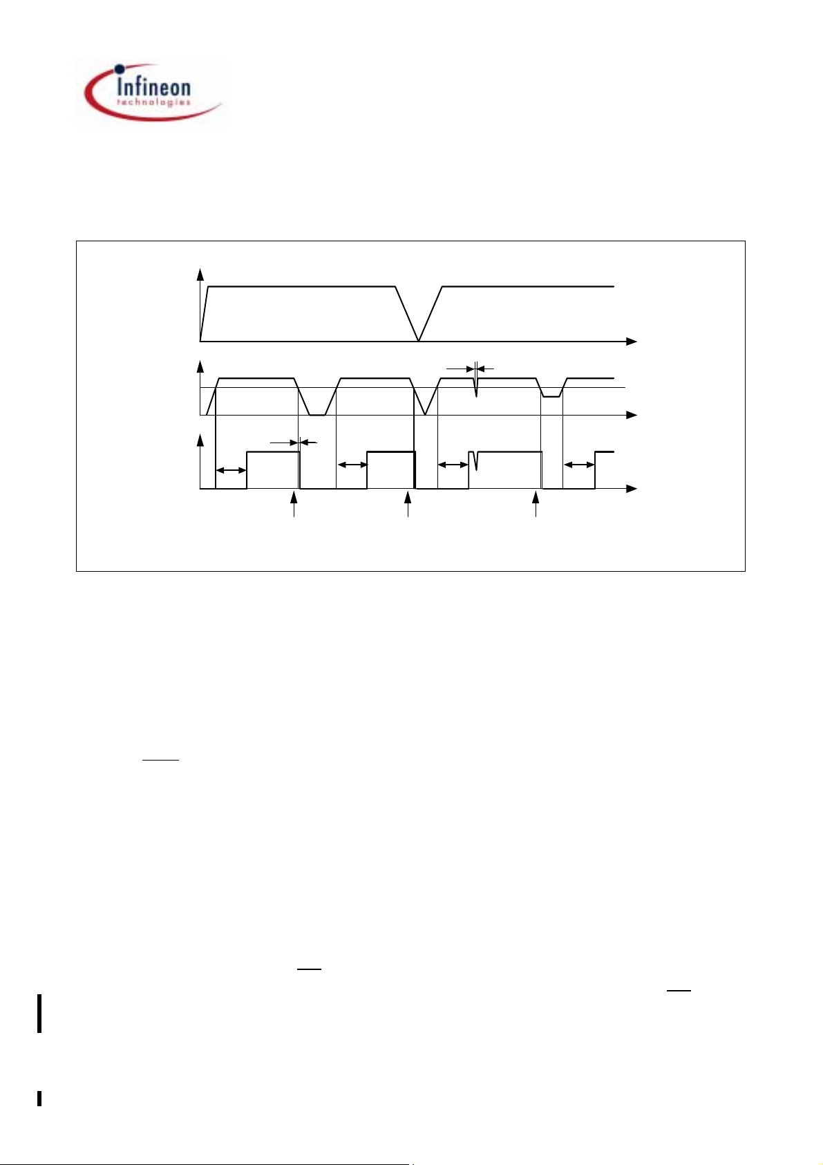
Figure 6 Window watchdog timing definition
Figure 6 shows some guideline s for designing the wa tchdog trigger timing taking the
oscillator deviation of different devices into account. Of importance (w.c.) is the
maximum of the closed window and the minimum of the open window in which the
trigger has to occur.
The length of the OW and CW can be modified by SPI command. If a change of the
window length is desired during the Watchdog function is operating please send the SPI
command with the new tim ing wit h a ’Watchd og tri gger Bit’ D1 5=1.In th is case the next
CW will directly start with the new length.
A minimum time gap of > 1/48 of the actual OW/CW time between a ’Watchdog disable’
and ’Watchdog enable’ SPI-command should be maintained. This allows the internal
Watchdog counters to be resetted. Thus after the enable command t he Watchdog will
start properly with a full CW of the adjusted length.
Data Sheet, Rev. 1.32 14 2004-10-15
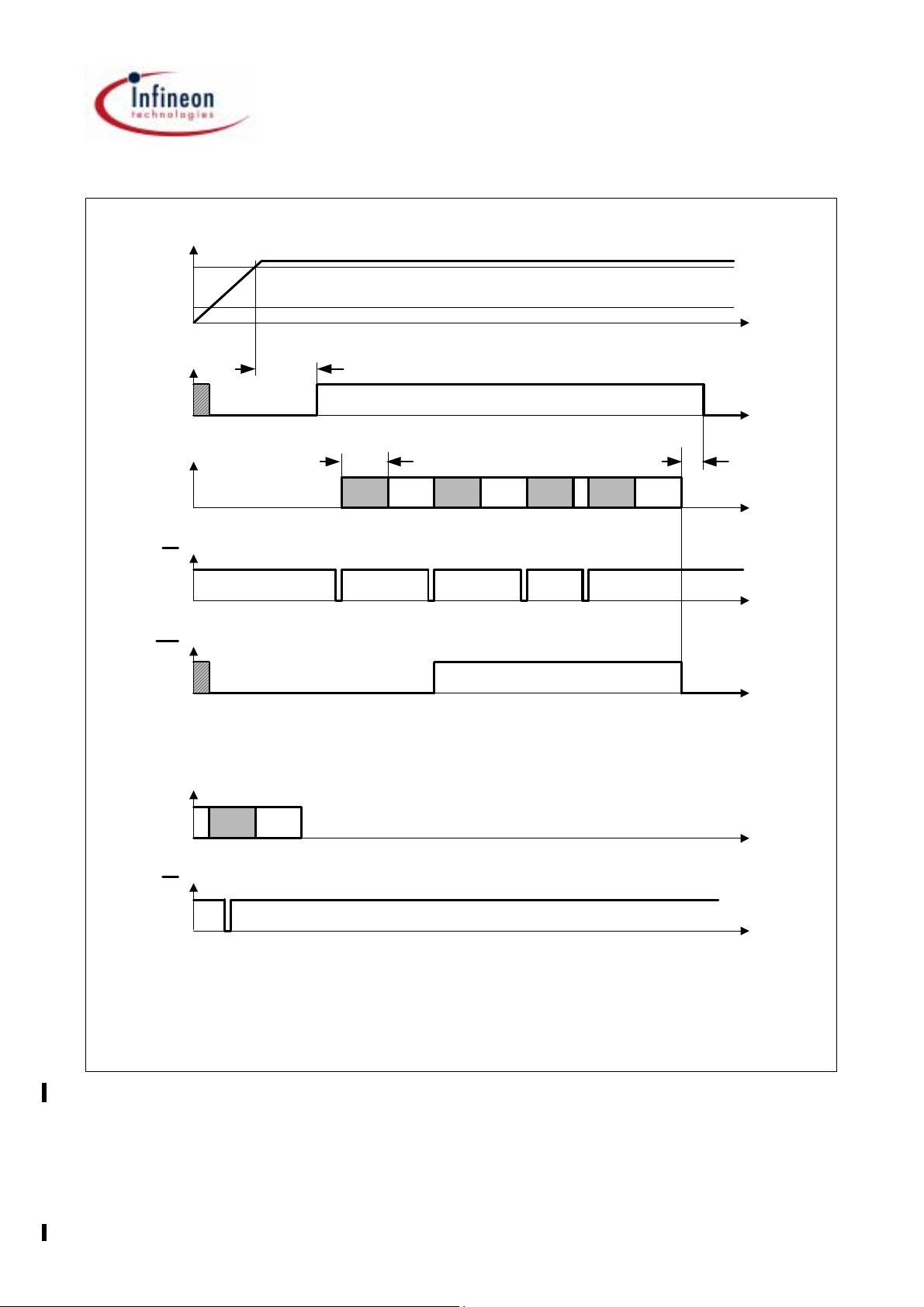
Perfect triggering after Power on Reset
V
Q_LDO1
V
Rth1
1V
t
R1
RES
TLE 6368 / SONIC
t
t
Watchdog
window
CS
ERR
Incorrect triggering
Watchdog
window
CW OW
CS
with WD-
trig=1
3) 4)
t
CW
CW OW CW OW CW CW OW
2)2)2)1)
t
SR
t
t
t
t
t
1) Watchdog enable command with no trigger: D0D9D14D15=0100
2) Watchdog trigger: D15=1
3) Pretrigger
4) Missing trigger
Legend: OW = Open window
CW = Closed window
Figure 7 Window watchdog timing
Figure 7 gives some timing information about the window watchdog. Looking at the
upper signals the perfect triggering of the watchdog is shown. When the 5V linear
regulator Q_LDO1 reaches its reset threshold, the reset delay time has to run off before
Data Sheet, Rev. 1.32 15 2004-10-15

TLE 6368 / SONIC
the closed window (CW) starts. Then three valid watchdog triggers are shown, no effect
on the reset line a nd/or error pin is ob served. With the miss ing watchdog trigger sign al
the error signal turns low immediately where the reset is asserted after another delay of
half the closed window time .
Also shown in the figure are two typica l failure modes, one pretrigger an d one missing
signal. In both cases the error s ignal will go low immedia tely the fai lure is detected with
the reset following after the half closed window time.
2.10 Overtemperature Protection
At a chip temperature of more than 150° an error and temperature flag is set and can be
read through the SPI. The device is switched off if the device reaches the
overtemperature threshold of 170°C. The overtemperature shutdown has a hysteresis to
avoid thermal pumping.
2.11 Power Down Mode
The TLE 6368 G1 / SONIC is starte d by a sta tic high s ignal at the wak e input or a hi gh
pulse with a minim um of 50µs duration at the Wake input (pi n 34). In order to avoid
instabilities of the device voltages applied to the Wake pin (pin 34) have to have a certain
slope, i.e. 1V/3µs. Voltages in the range between the turn on and turn off thresholds for
a few 100µs must be avoided!
By SPI command (“Sleep”-bit, D8, equals zero) all voltage regulators including the
switching regulator except the standby regulator can be turned off completely only if the
wake input is low. In the case the Wake input is permanently connected to battery the
device cannot be turned off by SPI command, it will always turn on again.
For stable “on” operation of the devi ce th e “Sleep ”-b it, D8 has to be set to high at ea ch
SPI cycle!
When powering the device again after power down the status of the SPI controlled
devices (e.g. trackers, watc hdog etc.) depends on th e output voltage on Q_LDO1. D id
the voltage at Q_LDO1 decrease below 3.3V the default status (given in the next section)
is set otherwise the last SPI command defines the status.
2.12 Serial Peripheral Interface
A standard 16 bit SPI is available for control and diagnost ics . It i s c apa ble to op erate in
a daisy chain. It can be written or read by a 16 bit SPI interface as well as by an 8 bit SPI
interface.
The 16-bit control word (write bit assignment, see Figure 8) i s rea d in vi a the dat a input
DI, synchronous to the clock input CLK supp lied by the µC begin ning with the LSB D0.
The diagnosis word appears in the same way synchronously at the data output DO (read
bit assignment, see figure 9), so with the first bit shifted on the DI line the first bit appears
on the DO line.
Data Sheet, Rev. 1.32 16 2004-10-15
TLE 6368 / SONIC
The transmission cycle be gins when the TLE 636 8 G1 / SONIC is sel ected by the “not
chip select” input CS
been read in at the DI line becomes the n ew control word. The DO output switch es to
tristate status at this point, thereby releasing the DO bus circuit for other uses. For details
of the SPI timing please refer to Figures 10 to 13.
The SPI will be reset to d efault valu es given i n the follow ing table “write bit me aning” if
the RAM good flag of Q_LDO1 indic ates a cold start (lower output voltage th an 3.3V).
The reset will be active as long as the power on reset is present so during the reset delay
time at power up no SPI commands are accepted.
The register content of the SPI - including watchdog timings and reset delay timings - is
maintained if the RAM good flag of Q_LDO1 indicates a warm start (i.e. Q_LDO1 did not
decrease below 3.3V).
2.12.1 Write mode
(H to L). After the CS input returns from L t o H, t he wo rd that has
The following tables s how the bit assignment to the different control functions, how to
change settings with the right bit combination and also the default status at power up.
2.12.2 Write mode bit assignment
BIT
Name
Default
WD_
NOT
OFF1
assigned
1 111111X 1 0100110
control
T1-
T2-
control
control
T6-
T4-
control
control
T5-
T6-
control
sleep
WD_
OFF2
WD2WD1reset 2reset 1
WD_
OFF3
D 15D8 D9 D10 D11 D12 D13 D14D7DO D1 D2 D3 D4 D5 D6
WD_
TRIG
Figure 8 Write Bit assignment
Write Bit meaning
Function Bit Combination Default
Not assigned D1 X X
Tracker 1 to 6 - control:
turn on/off the individual trackers
D2
D3
0: OFF
1: ON
1
D4
D5
D6
D7
Power down:
send device to sleep
Data Sheet, Rev. 1.32 17 2004-10-15
D8 0: SLEEP
1: NORMAL
1
TLE 6368 / SONIC
Write Bit meaning
Function Bit Combination Default
Reset timing:
Reset delay time t
valid at warm start
RES
Window watchdog timing:
Open window time t
closed window time t
and
OW
valid at warm start
CW
Window watchdog function:
Enable /disable window watchdog
Window watchdog trigger:
Enable / disable window watchdog trigger
2.12.3 Read mod e
D10D11 00: 64ms
10: 32ms
01: 16ms
11: 8ms
D12D13 00: 128ms
10: 64ms
01: 32ms
11: 16ms
D0D9D14 010: ON
1xx: OFF
x0x: OFF
xx1: OFF
D15 0: not triggered
1: trigger ed
11
00
101
0
Below the status information word and the bit assignments for diagnosis are shown.
2.12.3.1Read mode bit assignment
BIT
Name
Default
warn
T1-
status
status
status
status
status
status
RAM
Good 1
ERROR
temp_
0 1111110 0 1000000
T6-
T5-
T4-
T3-
T2-
RAM
Good 2
WD
Window
R-Error3R-Error2R-Error1
WD
Error
D 15D8 D9 D10 D11 D12 D13 D14D7DO D1 D2 D3 D4 D5 D6
DC/DC
status
Figure 9 Read Bit assignment
Error bit D0:
The error output ERR
is low and the error bit indic ates fail function if the tempera ture
prewarning or the watchdog error is active, further if one RAM good indicates a cold start
or if a voltage tracker does not settle within 1ms when it is turned on.
Data Sheet, Rev. 1.32 18 2004-10-15

TLE 6368 / SONIC
Read Bit meaning
Function Type Bit Combination Default
Error indication,
explanation see below this
Latched D0 0: normal operation
1: fail function
table
Overtemperature warning Not latched D1 0: normal operation
1: prewarning
Status of Tracker Output
Q_T[1:6],only if output is
ON
Not latched D2
D3
D4
D5
D6
D7
1: settled output
voltage
0:Tracker turned
off or shorted
output. Also open
load may possibly
be indicated as 0.
Indication of cold start/
warm start, Q_LDO1
Indication of cold start/
warm start, Q_LDO2
Indication for open or
closed window
Latched D8 0: cold start
1: warm start
Latched D9 0: cold start
1: warm start
Not latched D10 0: open window
1: closed window
0
0
1
1)
0
0
0
Reset condition at output
Q_LDO1
Reset condition at output
Q_LDO2
Reset condition at output
Q_LDO3
Not latched D11 0: normal operation
1: Reset R1
Not latched D12 0: normal operation
1: Reset R2
Not latched D13 0: normal operation
1: Reset R3
Watchdog Error Latched D14 0: normal operation
1: WD error
DC/DC converter status Not latched D15 0: off
1: on
1)
Min. load current to avoid ’0’ si gnal caused by open load is 2mA.
0
0
0
0
1
Data Sheet, Rev. 1.32 19 2004-10-15

2.12.4 SPI Timings
CS High to Low & rising edge of CLK: DO is enabled.
Status information is transferred to Output Shift Register
C
S
TLE 6368 / SONIC
e.g.
T
c
r
a
o
CLK
DI
DO
c
k
r
t
n
CS Low to High: Data from Register
time
are transferred to e.g. Trackers
0
Data In (N)
D2 D3
D1D0
151413321
01
Data In (N+1)
D1
D15D14D13
D0
+
+
DI: Data will be accepted on the falling edge of CLK-Signal
Data Out (N)
D1
D0
D0
Data Out (N-1)
D3D2D1
D15D14D13
DO: State will change on the rising edge of CLK-Signal
-
e
r
l
o
Setting (N-1)
Setting (N)
e.g.
-
r
e
T
s
r
k
a
c
s
u
t
a
t
Status (N-1)
Status (N)
Figure 10 SPI Data Transfer Timing
Data Sheet, Rev. 1.32 20 2004-10-15

TLE 6368 / SONIC
Figure 11 SPI-Input Timing
t
rIN
CLK
DO
DO
(low to high)
t
VADO
(high to low)
t
<10ns
fIN
0.7 V
Q_LDO1
50%
0.2 V
Q_LDO1
t
rDO
90%
10%
t
fDO
90%
10%
Figure 12 DO Valid Data Delay Time and Valid Time
Data Sheet, Rev. 1.32 21 2004-10-15

TLE 6368 / SONIC
t
fIN
CS
DO
t
ENDO
DO
Figure 13 DO Enable and Disable Time
t
DISDO
t
rIN
<10ns
10k
Ω
Pullup
to V
Q_LDO1
10k
Ω
Pulldown
to GND
0.7 V
50%
0.2 V
50%
50%
Q_LDO1
Q_LDO1
Data Sheet, Rev. 1.32 22 2004-10-15

TLE 6368 / SONIC
3 Characteristics
3.1 Absolute Maximum Ratings
Item Parameter Symbol Limit Values Unit Test Condition
Min. Max.
3.1.1 Supply Voltage Input IN
Voltage
Voltage
Current
V
V
I
IN
IN
IN
-0.5 60
-1.0 60
––
V
V
–
3.1.2 Buck-Switch Output SW
Voltage
Current
V
I
SW
SW
-2 VS+0.5
––
V
–
3.1.3 Feedback and Linear Voltage Regulator Input
Voltage
Current
V
FB/L_IN
I
FB/L_IN
-0.5 8
––
V
–
3.1.4 Bootstrap Connector Bootstrap
Voltage
Voltage V
Current I
V
Bootstrap
Bootstrap
Bootstrap
V
SW
0.5V
-
V
SW
10V
+
-0.5 70
––
V
V
–
–
Tj = -40 °C
–
–
Internally limited
3.1.5 Boost Input
Voltage
Current
V
Boost
I
Boost
-0.5 60
––
V
–
–
Internally limited
3.1.6 Slope Control Input Slew
Voltage
Current
V
I
Slew
Slew
-0.5 6
––
V
–
–
Internally limited
3.1.7 Charge Pump Capacitor Connector C-
Voltage
V
CL
-0.5 V
FB/L_IN
V
+0.5
Current I
Data Sheet, Rev. 1.32 23 2004-10-15
CL
-150 +150
mA

3.1.8 Charge Pump Capacitor Connector C+
TLE 6368 / SONIC
Voltage
Current I
V
CH
CH
-0.5 13
-150 +150 mA
3.1.9 Charge Pump Storage Capacitor CCP
Voltage
Current I
V
CCP
CCP
-0.5 12
-150 –
3.1.10 Standby Voltage Regulator output Q_STB
Voltage
Current
V
Q_Stb
I
Q_Stb
-0.5 6
––
3.1.11 Voltage Regulator output voltage Q_LDO1
Voltage
Current
V
Q_LDO1
I
Q_LDO1
-0.5 6
––
3.1.12 Voltage Regulator output voltage Q_LDO2
Voltage
Current
V
Q_LDO2
I
Q_LDO2
-0.5 6
––
V
V
mA
V
–
V
–
V
–
–
Internally limited
–
Internally limited
–
Internally limited
3.1.13 Voltage Regulator output voltage Q_LDO3
Voltage
Current
V
Q_LDO3
I
Q_LDO3
-0.5 6
––
3.1.14 Voltage Tracker output voltage Q_T1
Voltage
Current
V
Q_T1
I
Q_T1
-5 60
––
3.1.15 Voltage Tracker output voltage Q_T2
Voltage
Current
V
Q_T2
I
Q_T2
-5 60
––
3.1.16 Voltage Tracker output voltage Q_T3
Voltage
Current
V
Q_T3
I
Q_T3
-5 60
––
3.1.17 Voltage Tracker output voltage Q_T4
Voltage
V
Q_T4
-5 60
V
–
V
mA
V
mA
V
mA
V
–
Internally limited
–
Internally limited
–
Internally limited
–
Internally limited
–
Current
Data Sheet, Rev. 1.32 24 2004-10-15
I
Q_T4
––
mA
Internally limited

3.1.18 Voltage Tracker output voltage Q_T5
TLE 6368 / SONIC
Voltage
Current
V
Q_T5
I
Q_T5
-5 60
––
3.1.19 Voltage Tracker output voltage Q_T6
Voltage
Current
V
Q_T6
I
Q_T6
-5 60
––
3.1.20 Select Input SEL
Voltage
Current
V
I
SEL
SEL
-0.5 6
––
3.1.21 Wake Up Input Wake
Voltage
Current
V
Wake
I
Wake
-0.5 60
––
3.1.22 Reset Output R1
Voltage
Current
V
I
R1
R1
-0.5 6
––
V
mA
V
mA
V
–
V
–
V
–
–
Internally limited
–
Internally limited
–
Internally limited
–
–
3.1.23 Reset Output R2
Voltage
Current
V
I
R2
R2
3.1.24 Reset Output R3
Voltage
Current
V
I
R3
R3
3.1.25 SPI Data Input DI
Voltage
Current
V
I
DI
DI
3.1.26 SPI Data Output DO
Voltage
Current
V
I
DO
DO
3.1.27 SPI Clock Input CLK
Voltage
V
CLK
-0.5 6
––
-0.5 6
––
-0.5 6
––
-0.5 6
––
-0.5 6
V
–
V
–
V
–
V
–
V
–
–
–
–
Internally limited
–
Current
Data Sheet, Rev. 1.32 25 2004-10-15
I
CLK
––
–

3.1.28 SPI Chip Select Not Input CS
TLE 6368 / SONIC
Voltage V
Current
CS
I
CS
3.1.29 Error Output Pin
Voltage
Current
V
I
ERR
ERR
3.1.30 Thermal Resistance
Junction-
R
thja
ambient
Junction-
R
thja
ambient
Junction-
R
thjc
case
3.1.31 Temperature
Junction
T
j
temperature
Junction
T
jt
temperature
transient
-0.5 6
––
-0.5 6
––
37
29
V
–
V
–
K/W
K/W
–
–
Internally limited
1)
PCB heat sink area
300mm
1)
PCB heat sink area
600mm
2
2
– 2 K/W
-40 150 °C
175 °C lifetime=TBD
Storage
T
stg
-50 150 °C
temperature
3.1.32 ESD
ESD V
1) Package mounted on FR4 47x50x1.5mm3; 70µ Cu, zero airflow
ESD
-1 1 kV HBM-Model
Note: Maximum ratings are absol ute ratings; exceeding any one of thes e values may
cause irreversible damage to the integrated circuit.
Data Sheet, Rev. 1.32 26 2004-10-15

3.2 Functional Range
TLE 6368 / SONIC
-40°C < T
< 150 °C
j
Item Parameter Symbol Limit Values Unit Condition
min. max.
Supply
Voltage
Supply
V
IN, min
V
IN, max
5.5 V VIN increased from
0V;
WAKE
=5V;
=400mA;
=200mA
V
I
Q_LDO1
I
Q_LDO2
60 V
Voltage
Ripple at
FB/L_IN
V
FB/L_IN
ripple
0150mV
PP
Note: Within the functional range the IC can be operated . The electrical characteristics,
however, are not guaranteed over this full functional range.
Data Sheet, Rev. 1.32 27 2004-10-15
3.3 Recommended Operation Range
TLE 6368 / SONIC
-40°C < T
< 150 °C
j
Item Parameter Symbol Limit Values Unit Condition
min. typ. max.
Buck
L
B
18 100 µH
1)
Inductor
Buck
Capacitor
C
B
10 µF ESR <0.15 Ω,
ceramic
capacitor (X7R)
recommended
Bootstrap
C
BTP
2% of C
B
Capacitor
SLEW
R
SLEW
020kΩ
resistor
Linear
regulator
C
Q_LDO1-3
470 nF ceramic
capacitor (X7R)
capacitors
Tracker
bypass
C
Q_T1-6
1µFceramic
capacitor (X7R)
capacitors
1)
SPI rise and
t
r,f
200 ns
fall timings,
CS
, DI, CLK
1)
C
needs about LB=47µH to avoid instabilities
B, min
Data Sheet, Rev. 1.32 28 2004-10-15

TLE 6368 / SONIC
3.4 Electrical Characteristics
The electrical characteristics involve the spread of values guaranteed within the
specified supply voltage and ambient temperature range. Typic al values represent the
median values at room temperature, which are related to production processes.
-40 < T
<150 °C; VIN=13.5V unless otherwise specified
j
Item Parameter Symbol Limit Values Unit Test Conditions
min. typ. max.
Buck regulator
3.4.1 Switching
f
SW
280 370 425 kHz
frequency
3.4.2 Current
t
r_I_SW
20 ns RSL=0Ω;
1)
transition
time, min.,
rising edge
3.4.3 Current
t
r_I_SW
100 ns RSL=20kΩ;
1)
transition
time, max.,
rising edge
3.4.4 Current
t
f_I_SW
20 ns RSL=0Ω;
1)
transition
time, min.,
falling edge
3.4.5 Current
t
f_I_SW
100 ns RSL=20kΩ;
1)
transition
time, max.,
falling edge
3.4.6 Voltage rise /
t
f_V_SW
25 ns
1)
fall time
3.4.7 Static on
resistance
3.4.8 Static on
resistance
3.4.9 Current limit I
3.4.10 Output
voltage
Data Sheet, Rev. 1.32 29 2004-10-15
R
R
MAX
V
ON
ON
OUT
160 mΩ Tj=25°C
in static operation
280 400 mΩ Tj=150°C
in static operation
1.5 3.2 A V
5.40 6.05 V I
V
FB/L_IN
=1.5A
OUT
=13.5 V
IN
=5.4V

TLE 6368 / SONIC
-40 < T
<150 °C; VIN=13.5V unless otherwise specified
j
Item Parameter Symbol Limit Values Unit Test Conditions
min. typ. max.
3.4.11 Output
voltage
3.4.12 Bootstrap
V
OUT
I
BTSTR
5.4 6.3 V I
80 160 220 µA
OUT
=13.5 V
V
IN
=0.1A
charging
current at
start-up
3.4.13 Bootstrap
voltage
(internal
V
BTSTR
10 15 V V
FB/L_IN
=6.5V,
Buck converter
off
charge
pump)
3.4.14 Bootstrap
undervoltage
V
BTSTR,
turn on
59V
lockout, Buck
turn on
threshold
3.4.15 Bootstrap
undervoltage
lockout,
hysteresis
3.4.16 External
charge
pump
voltage
3.4.17 Max. Duty
Cycle
3.4.18 Min. Duty
Cycle
Voltage Regulator Q_LDO1
3.4.19 Output
voltage
3.4.20 Output
voltage
V
BTSTR,
turn on
V
BTSTR,
turn off
V
CCP
duty
duty
V
Q1
V
Q1
-
max
min
2.5 V
7.9 11.0 V I
Q_LDO1
V
C
C
FB/L_IN
=100nF,
FLY
=220nF
CCP
= 800mA,
=6.0V,
95 % Switching
operation
0%Static-off
operation
4.9 5.1 V 100mA < I
< 800mA
5.0 V I
Q_LDO1
= 800mA
Q_LDO1
Data Sheet, Rev. 1.32 30 2004-10-15

TLE 6368 / SONIC
-40 < T
<150 °C; VIN=13.5V unless otherwise specified
j
Item Parameter Symbol Limit Values Unit Test Conditions
min. typ. max.
3.4.21 Load
Regulation
3.4.22 Current limit I
3.4.23 Ripple
∆V
Q_LDO1
40 mV 100mA< I
<800mA;
=5.5V
=4V
Q_LDO1limit
V
800 1050 1400 mA V
FB/L_IN
Q_LDO1
PSRR1 26 40 dB f=330kHz;
Q_LDO1
1)
rejection
3.4.24 Output
Capacitor
C
Q_LDO1
470 nF Ceramic type,
value for stability
Voltage Regulator Q_LDO2
3.4.25 Output
voltage 3.3V
V
Q_LDO2
3.14 3.46 V 50mA < I
400mA;
Q_LDO2
3.3V mode
3.4.26 Output
voltage 3.3V
V
Q_LDO2
3.32 V I
Q_LDO2
=400mA;
3.3V mode
<
3.4.27 Output
voltage 2.6V
3.4.28 Output
voltage 2.6V
3.4.29 Output
voltage 2.6V
3.4.30 Load
Regulation
3.4.31 Load
Regulation
3.4.32 Current limit I
V
Q_LDO2
V
Q_LDO2
V
Q_LDO2
∆V
Q_LDO2
∆V
Q_LDO2
Q_LDO2limit
2.500 2.750 V 50mA < I
400mA;
2.6V mode
2.62 V I
Q_LDO2
=400mA;
2.6V mode
2.50 2.70 V 85mA < I
400mA;
2.6V mode
50 mV 50mA< I
<400mA;
V
FB/L_IN
=5.5V
3.3V mode
50 mV 50mA< I
<400mA;
V
FB/L_IN
=5.5V
2.6V mode
500 650 850 mA V
Q_LDO2
3.3V mode
Q_LDO2
Q_LDO2
Q_LDO2
Q_LDO2
= 2.8V;
<
<
3.4.33 Current limit I
Q_LDO2limit
500 650 850 mA V
Q_LDO2
= 2V;
2.6V mode
Data Sheet, Rev. 1.32 31 2004-10-15

TLE 6368 / SONIC
-40 < T
<150 °C; VIN=13.5V unless otherwise specified
j
Item Parameter Symbol Limit Values Unit Test Conditions
min. typ. max.
3.4.34 Ripple
PSRR2 26 40 dB f=330kHz;
1)
rejection
3.4.35 Output
Capacitor
C
Q_LDO2
470 nF Ceramic type,
value for stability
Voltage Regulator Q_LDO3
3.4.36 Output
voltage 3.3V
V
Q_LDO3
3.14 3.46 V 20mA < I
300mA;
Q_LDO3
3.3V mode
3.4.37 Output
voltage 3.3V
3.4.38 Output
voltage 2.6V
V
Q_LDO3
V
Q_LDO3
3.32 V I
Q_LDO3
=300mA;
3.3V mode
2.500 2.750 V 20mA < I
300mA;
Q_LDO3
2.6V mode
<
<
3.4.39 Output
voltage 2.6V
3.4.40 Load
Regulation
3.4.41 Load
Regulation
3.4.42 Current limit I
3.4.43 Current limit I
3.4.44 Ripple
rejection
3.4.45 Output
Capacitor
V
Q_LDO3
2.625 V I
Q_LDO3
=300mA;
2.6V mode
∆V
Q_LDO3
30 mV 20mA< I
Q_LDO3
<300mA;
V
FB/L_IN
=5.5V
3.3V mode
∆V
Q_LDO3
30 mV 20mA< I
Q_LDO3
<300mA;
V
FB/L_IN
=5.5V
2.6V mode
Q_LDO3
limit
Q_LDO3
limit
350 500 600 mA V
3.3V mode
350 500 600 mA V
2.6V mode
Q_LDO3
Q_LDO3
=4V;
=2.8V;
PSRR3 26 40 dB f=330kHz;
C
Q_LDO3
470 nF Ceramic type,
value for stability
1)
Voltage Tracker Q_T1
Data Sheet, Rev. 1.32 32 2004-10-15

TLE 6368 / SONIC
-40 < Tj <150 °C; VIN=13.5V unless otherwise specified
Item Parameter Symbol Limit Values Unit Test Conditions
min. typ. max.
3.4.46 Output
voltage
tracking
accuracy
3.4.47 Output
voltage
tracking
accuracy
3.4.48 Overvoltage
threshold
3.4.49 Undervoltage
threshold
3.4.50 Current limit I
3.4.51 Ripple
rejection
3.4.52 Tracker load
capacitor
∆V
Q_T1
-15 -2 5 mV V
1mA < I
Q_T1-VQ_LDO1
Q_T1
17mA
∆V
Q_T1
V
OVQ_T1
V
UVQ_T1
-10 mV V
I
V
Q_T1,
nom
V
Q_T1
-
mV I
mV
1)
Q_T1-VQ_LDO1
= 17mA
Q_T1
= 0mA; 1)
Q_T1
15mV
Q_T1 limit
17 30 mA V
Q_T1
=4V
PSRR 26 dB f=330kHz;
C
Q_T1
1 µF Ceramic type,
minimum for
stability
;
<
;
1)
Voltage Tracker Q_T2
3.4.53 Output
voltage
tracking
accuracy
3.4.54 Output
voltage
tracking
accuracy
3.4.55 Overvoltage
threshold
3.4.56 Undervoltage
threshold
3.4.57 Current limit I
3.4.58 Ripple
rejection
∆V
Q_T2
-15 -2 5 mV V
1mA < I
Q_T2-VQ_LDO1
Q_T2
17mA
∆V
Q_T2
V
OVQ_T2
V
UVQ_T2
-10 mV V
I
V
Q_T2,
nom
V
Q_T2
-
mV I
mV
1)
Q_T2-VQ_LDO2
= 17mA
Q_T2
= 0mA;
Q_T2
15mV
Q_T2 limit
17 30 mA V
Q_T2
=4V
PSRR 26 dB f=330kHz;
;
<
;
1)
1)
Data Sheet, Rev. 1.32 33 2004-10-15

TLE 6368 / SONIC
-40 < Tj <150 °C; VIN=13.5V unless otherwise specified
Item Parameter Symbol Limit Values Unit Test Conditions
min. typ. max.
3. 4 .5 9 Tracker load
capacitor
Voltage Tracker Q_T3
3.4.60 Output
voltage
tracking
accuracy
3.4.61 Output
voltage
tracking
accuracy
3.4.62 Overvoltage
threshold
3.4.63 Undervoltage
threshold
C
Q_T2
∆V
Q_T3
∆V
Q_T3
V
OVQ_T3
V
UVQ_T3
1 µF Ceramic type,
minimum for
stability
-15 -2 5 mV V
Q_T3-VQ_LDO1
1mA < I
Q_T3
<
17mA
-10 mV V
V
Q_T3,
nom
V
Q_T3
-
mV I
mV
Q_T3-VQ_LDO3
I
= 17mA
Q_T3
= 0mA;
Q_T3
1)
1)
15mV
;
;
3.4.64 Current limit I
3.4.65 Ripple
rejection
3. 4 .6 6 Tracker load
capacitor
Voltage Tracker Q_T4
3.4.67 Output
voltage
tracking
accuracy
3.4.68 Output
voltage
tracking
accuracy
3.4.69 Overvoltage
threshold
Q_T3 limit
17 30 mA V
Q_T3
=4V
PSRR 26 dB f=330kHz;
C
Q_T3
1 µF Ceramic type,
minimum for
stability
∆V
Q_T4
-15 -2 5 mV V
Q_T4-VQ_LDO1
1mA < I
Q_T4
17mA
∆V
Q_T4
V
OVQ_T4
-8 mV V
I
V
Q_T4,
nom
mV I
Q_T4-VQ_LDO4
= 17mA
Q_T4
= 0mA;
Q_T4
1)
;
<
;
1)
Data Sheet, Rev. 1.32 34 2004-10-15

TLE 6368 / SONIC
-40 < T
<150 °C; VIN=13.5V unless otherwise specified
j
Item Parameter Symbol Limit Values Unit Test Conditions
min. typ. max.
3.4.70 Undervoltage
threshold
3.4.71 Current limit I
3.4.72 Ripple
V
UVQ_T4
V
Q_T4
-
mV
15mV
Q_T4 limit
17 30 mA V
PSRR 26 dB f=330kHz;
1)
Q_T4
=4V
1)
rejection
3.4.73 Tracker load
capacitor
C
Q_T4
1 µF Ceramic type,
minimum for
stability
Voltage Tracker Q_T5
3.4.74 Output
voltage
tracking
∆V
Q_T5
-15 -1 5 mV V
1mA < I
17mA
Q_T5-VQ_LDO1
<
Q_T5
;
accuracy
3.4.75 Output
voltage
tracking
accuracy
3.4.76 Overvoltage
threshold
3.4.77 Undervoltage
threshold
3.4.78 Current limit I
3.4.79 Ripple
rejection
3.4.80 Tracker load
capacitor
Voltage Tracker Q_T6
3.4.81 Output
voltage
tracking
accuracy
∆V
Q_T5
V
OVQ_T5
V
UVQ_T5
-9 mV V
I
V
Q_T5,
nom
V
Q_T5
-
mV I
mV
1)
Q_T5-VQ_LDO5
= 17mA
Q_T5
= 0mA;
Q_T5
15mV
Q_T5 limit
17 30 mA V
Q_T5
=4V
PSRR 26 dB f=330kHz;
C
Q_T5
1 µF Ceramic type,
minimum for
stability
∆V
Q_T6
-15 -1 5 mV V
1mA < I
Q_T6-VQ_LDO1
Q_T6
17mA
;
1)
1)
;
<
Data Sheet, Rev. 1.32 35 2004-10-15

TLE 6368 / SONIC
-40 < T
<150 °C; VIN=13.5V unless otherwise specified
j
Item Parameter Symbol Limit Values Unit Test Conditions
min. typ. max.
3.4.82 Output
voltage
∆V
Q_T6
-9 mV V
I
Q_T6-VQ_LDO6
= 17mA
Q_T6
;
tracking
accuracy
3.4.83 Overvoltage
V
OVQ_T6
V
Q_T6
mV I
Q_T6
= 0mA;
1)
threshold
3.4.84 Undervoltage
threshold
3.4.85 Current limit I
3.4.86 Ripple
V
UVQ_T6
V
Q_T6
-
mV
15mV
Q_T6 limit
17 30 mA V
PSRR 26 dB f=330kHz;
1)
Q_T6
=4V
1)
rejection
3. 4 .8 7 Tracker load
capacitor
C
Q_T6
1 µF Ceramic type,
minimum for
stability
Standby Regulator
3.4.88 Output
voltage
3.4.89 Current limit I
3.4.90 Standby
load
capacitor
Current consumption in off-mode and Wake block
3.4.91 Supply
current from
battery
3.4.92 Supply
current from
battery
3.4.93 Turn on
Wake-up
threshold
V
Q_STB
Q_STB limit
C
Q_STB
I
q,off
I
q,off
V
wake th, on
2.2 2.4 2.6 V 0µA
Q_STB
<500µA
=2V
<I
136mAV
Q_STB
100 nF Ceramic type,
minimum for
stability
10 30 µA VIN=13.5V,
=0
V
wake
I
Q_STB
=0µA
10 30 µA VIN=42V,
V
=0
wake
I
2.4 2.8 V V
=0µA
Q_STB
increasing
wake
Data Sheet, Rev. 1.32 36 2004-10-15

TLE 6368 / SONIC
-40 < T
<150 °C; VIN=13.5V unless otherwise specified
j
Item Parameter Symbol Limit Values Unit Test Conditions
min. typ. max.
3.4.94 Turn off
V
wake th, off
1.8 2.35 V V
decreasing
wake
Wake-up
threshold
3.4.95 Wake-up
I
wake
50 150 µA V
wake
=5V
input current
3.4.96 W ake up
input on time
t
wake,min
41050µsV
V
>
wake
wake th, max
1)
;
Reset R1
3.4.97 Reset
threshold
V
RTH
Q_LDO1, de
4.5 4.65 4.8 V V
decreasing
Q_LDO1
Q_LDO1
3.4.98 Reset
threshold
V
RTH
Q_LDO1, in
4.55 4.70 4.9 V V
increasing
Q_LDO1
Q_LDO1
3.4.99 Reset output
low voltage
3.4.100 Reset output
low voltage
3.4.101 Reset output
low sink
current
3.4.102 Reset High
leakage
current
Reset R2
3.4.103 Reset
threshold
Q_LDO2
3.4.104 Reset
threshold
hysteresis
Q_LDO2
V
R1 L
V
R1 L
I
R1 L
I
R1 H
V
RTH
Q_LDO2, de
V
RTH
Q_LDO2, in
V
RTH
Q_LDO2, de
0.4 V IR1=1.6mA;
V
Q_LDO1
0.3 V IR1=0.3mA;
V
Q_LDO1
10 µA V
Q_LDO1
> 25°C
T
j
1µA
2.6 2.8 3.0 V 3.3V mode;
V
Q_LDO2
decreasing
40 mV 3.3V mode
-
=5V
=1V
=0.75V;
Data Sheet, Rev. 1.32 37 2004-10-15

TLE 6368 / SONIC
-40 < T
<150 °C; VIN=13.5V unless otherwise specified
j
Item Parameter Symbol Limit Values Unit Test Conditions
min. typ. max.
3.4.105 Reset
threshold
Q_LDO2
3.4.106 Reset
threshold
hysteresis
Q_LDO2
3.4.107 Reset output
low voltage
3.4.108 Reset output
low voltage
3.4.109 Reset output
low sink
V
RTH
Q_LDO2, de
V
RTH
Q_LDO2, in
V
RTH
Q_LDO2, de
V
R2 L
V
R2 L
I
R2 L
2.3 2.4 2.5 V 2.6V mode;
V
Q_LDO2
decreasing
40 mV 2.6V mode
-
0.4 V IR2=1.6mA;
V
Q_LDO2
0.3 V IR2=0.3mA;
V
Q_LDO2
10 µA V
Q_LDO2
> 25°C
T
j
=2.5V
=1V
=0.75V;
current
3.4.110 Reset High
leakage
current
Reset R3
3.4.111 Reset
threshold
Q_LDO3
3.4.112 Reset
threshold
hysteresis
Q_LDO3
3.4.113 Reset
threshold
Q_LDO3
3.4.114 Reset
threshold
hysteresis
Q_LDO3
I
R2 H
V
RTH
Q_LDO3, de
V
RTH
Q_LDO3, in
V
RTH
Q_LDO3, de
V
RTH
Q_LDO3, de
V
RTH
Q_LDO3, in
V
RTH
Q_LDO3, de
1µA
2.7 2.85 3.0 V 3.3V mode;
V
Q_LDO3
decreasing
40 mV 3.3V mode
-
2.3 2.35 2.5 V 2.6V mode;
V
Q_LDO3
decreasing
40 mV 2.6V mode
-
3.4.115 Reset output
V
R3 L
low voltage
Data Sheet, Rev. 1.32 38 2004-10-15
0.4 V IR3=1.6mA;
V
Q_LDO3
=3.3V

TLE 6368 / SONIC
-40 < T
<150 °C; VIN=13.5V unless otherwise specified
j
Item Parameter Symbol Limit Values Unit Test Conditions
min. typ. max.
3.4.116 Reset output
low voltage
3.4.117 Reset output
low sink
V
I
R3 L
R3 L
0.3 V IR3=0.3mA;
V
10 µA V
T
Q_LDO3
Q_LDO3
> 25°C
j
=1V
=0.75V;
current
3.4.118 Reset High
I
R3 H
1µA
leakage
current
3.4.119 Reset
reaction time
t
rr
1210µs
1)
Valid for R1, R2
and R3
3.4.120 Reset Delay
t
NORM,RES
0.75 1 1.25 1
Norm factor
3.4.121 Reset Delay
time
t
RES
0.75 1 1.25 t
RES(SPI)
Valid for R1, R2
and R3; t
RES (SPI)
is defined by the
SPI word (see
section 2.12)
RAM Good
3.4.122 V
3.4.123 V
3.4.124 V
threshold V
Q1
threshold V
Q2
threshold V
Q2
Window Watchdog
3.4.125 Closed
window time
tolerance
3.4.126 Open
window time
tolerance
Th Q1
Th Q2
Th Q2
t
CW_tol
t
OW_tol
2.3 2.8 3.3 V
1.2 1.4 1.7 V 3.3V mode
1.2 1.4 1.7 V 2.6V mode;
0.75 1 1.25 Multiply with
watchdog
window time set
by SPI to obtain
the limits (2.12)
0.75 1 1.25 Multiply with
watchdog
window time set
by SPI to obtain
the limits (2.12)
1)
Data Sheet, Rev. 1.32 39 2004-10-15

TLE 6368 / SONIC
-40 < T
<150 °C; VIN=13.5V unless otherwise specified
j
Item Parameter Symbol Limit Values Unit Test Conditions
min. typ. max.
3.4.127 Watchdog
t
WRL
t
RES
reset low
time
3.4.128 Watchdog
t
SR
tCW/2
reset delay
time
Error Output ERR
3.4.129 H-output
voltage level
3.4.130 L-output
V
V
ERR,H
ERR,L
V
– 2.0
Q_LDO1
V
Q_LDO1
– 0.7
–VI
–0.30.5VI
ERR, H
ERR, L
=1 mA
=– 1.6 mA
voltage level
SPI
3.4.131 SPI clock
frequency
f
CLK
02.5MHzProduction test
up to 1MHz;
For 2.5MHz:
1)
SPI Input DI
3.4.132 H-input
voltage
threshold
3.4.133 L-input
voltage
threshold
3.4.134 Hysteresis of
input voltage
3.4.135 Pull down
current
3.4.136 Input
capacitance
3.4.137 Input signal
rise time
3.4.138 Input signal
fall time
V
V
V
I
C
t
t
–
–
1)
V
Q_LDO1
Q_LDO1
<
IH
IL
IHY
I
I
–4070% of
V
Q_LDO1
20
36 – % of
V
Q_LDO1
50 200 500 mV
5 25 100 µA VDI = 0.2 *
–1015pF0V < V
5.25 V
r
f
– – 200 ns
– – 200 ns
1)
1)
SPI Clock Input CLK
Data Sheet, Rev. 1.32 40 2004-10-15

TLE 6368 / SONIC
-40 < Tj <150 °C; VIN=13.5V unless otherwise specified
Item Parameter Symbol Limit Values Unit Test Conditions
min. typ. max.
3.4.139 H-input
voltage
threshold
3.4.140 L-input
voltage
threshold
3.4.141 Hysteresis of
input voltage
3.4.142 Pull down
current
3.4.143 Input
capacitance
3.4.144 Input signal
rise time
3.4.145 Input signal
fall time
SPI Chip Select Input CS
V
V
V
I
C
t
t
IH
IL
IHY
I
I
–4070% of
V
Q_LDO1
20
36 – % of
V
Q_LDO1
50 200 500 mV
525100µA V
–1015pF0V < V
–
–
1)
CLK
V
Q_LDO1
= 0.2 *
Q_LDO1
<
5.25 V
r
f
– –200ns
– –200ns
1)
1)
3.4.146 H-input
voltage
threshold
3.4.147 L-input
voltage
threshold
3.4.148 Hysteresis of
input voltage
3.4.149 Pull up
current at pin
CS
3.4.150 Input
capacitance
3.4.151 Input signal
rise time
3.4.152 Input signal
fall time
V
V
V
I
I, CS
C
t
r
t
f
IH
IL
IHY
I
–3970% of
V
Q_LDO1
20
35 – % of
V
Q_LDO1
50 200 500 mV
–
–
1)
– 100 – 25 – 5 µA VCS = 0.2 *
V
Q_LDO1
–1015pF0V < V
Q_LDO1
5.25 V
– –200ns
– –200ns
1)
1)
<
Data Sheet, Rev. 1.32 41 2004-10-15

TLE 6368 / SONIC
-40 < T
<150 °C; VIN=13.5V unless otherwise specified
j
Item Parameter Symbol Limit Values Unit Test Conditions
min. typ. max.
Logic Output DO
3.4.153 H-output
voltage level
3.4.154 L-output
V
V
DOH
DOL
V
– 1.0
Q_LDO1
V
Q_LDO1
– 0.8
–VI
– 0.2 0.4 V I
=1 mA
DOH
= – 1.6 mA
DOL
voltage level
3.4.155 Tri-state
leakage
current
3.4.156 Tri-state
input
capacitance
I
DO_TRI
C
DO
– 10 – 10 µA VCS = V
0V < V
V
Q_LDO1
–1015pFVCS=V
0V < V
5.25 V
Q_LDO1
DO
Q_LDO1
Q_LDO1
<
<
;
Data Input Timing
3.4.157 Clock period
3.4.158 Clock high
time
3.4.159 Clock low
time
3.4.160 Clock low
before CS
low
3.4.161 CS setup
time
3.4.162 CLK setup
time
3.4.163 Clock low
after CS
high
3.4.164 DI setup time t
3.4.165 DI hold time t
t
pCLK
t
CLKH
t
CLKL
t
bef
t
lead
t
lag
t
beh
DISU
DIHO
1000 – – ns
500 – – ns
500 – – ns
500 – – ns
500 – – ns
500 – – ns
500 – – ns
250 – – ns
250 – – ns
1)
1)
1)
1)
1)
1)
1)
1)
1)
Data Output Timing
Data Sheet, Rev. 1.32 42 2004-10-15
TLE 6368 / SONIC
-40 < Tj <150 °C; VIN=13.5V unless otherwise specified
Item Parameter Symbol Limit Values Unit Test Conditions
min. typ. max.
3.4.166 DO rise time t
3.4.167 DO fall time
3.4.168 DO enable
time
3.4.169 DO disable
time
3.4.170 DO valid time
General
3.4.171 Temperature
warning flag
3.4.172 Over
Temperature
shutdown
3.4.173 Over-
Temperature
shutdown
Hysteresis
rDO
t
fDO
t
ENDO
t
DISDO
t
VADO
T
J,Flag
T
J,Shutdown
∆T
sd_hys
–50100nsCL = 100 pF
–50100nsCL = 100 pF
– –250nslow impe dan ce
– –250nshigh impedance
–100250nsVDO < 10%
V
> 90%
DO
= 100 pF
C
L
140 °C
150 170 200 °C
2)
2)
30 K
3.4.174 Delta of TWF
to TSD
1)
Specified by design, not s ubject to production test
2)
Simulated at w afer test only, no t absolutely measured
Data Sheet, Rev. 1.32 43 2004-10-15
T
J,Shutdown
- T
J,Flag
20 K

4 Typical performance
charcteristics
TLE 6368 G1 / SONIC
Buck converter switching frequency
vs. junction temperature
420
f
SW
kHz
400
380
360
340
320
300
280
-50 -20 10 40 70 100 130 160
°C
Buck convert er DMOS on-resistance
vs. junction temperature
400
R
ON
m
Ω
350
300
250
200
150
100
50
T
j
-50 -20 10 40 70 100 130 160
°C
T
j
Buck converter output voltage at 1.5A load
vs. junction temperature
6.0
V
FB/L_IN
V
5.9
5.8
5.7
5.6
5.5
5.4
5.3
-50 -20 10 40 70 100 130 160
°C
T
j
Buck converter current limit
vs. junction temperature
4.0
I
MAX
A
3.5
3.0
2.5
2.0
1.5
1.0
0.5
-50 -20 10 40 70 100 130 160
°C
T
j
Data Sheet, Rev. 1.32 44 2004-10-15

TLE 6368 G1 / SONIC
Start-up bootstrap charging current
vs. junction temperature
280
I
BTSTR
µA
240
200
160
120
80
40
0
-50 -20 10 40 70 100 130 160
T
°C
Bootstrap UV lockout, turn on threshold
vs. junction temperature
V
8.5
BTSTR,
turn on
V
8.0
7.5
7.0
6.5
6.0
5.5
5.0
j
-50 -20 10 40 70 100 130 160
T
°C
j
Device start-up voltage (acc. to spec. 3.2)
vs. junction temperature
6.0
V
IN
V
5.5
5.0
4.5
4.0
3.5
3.0
2.5
-50 -20 10 40 70 100 130 160
°C
T
j
Device wake up thresholds
vs. junction temperature
wake th
V
2.8
2.7
2.6
2.5
V
2.4
2.3
2.2
2.1
-50 -20 10 40 70 100 130 160
wake th , on
V
V
wake th, off
T
°C
j
Data Sheet, Rev. 1.32 45 2004-10-15

TLE 6368 G1 / SONIC
Q_LDO1 output voltage at 800mA load
vs. junction temperature
5.20
V
Q_LDO 1
V
5.15
5.10
5.05
5.00
4.95
4.90
4.85
-50 -20 10 40 70 100 130 160
°C
Q_LDO1 current limit
vs. junction temperature
1400
I
Q_LDO1
V
1300
1200
1100
1000
900
800
700
T
j
-50 -20 10 40 70 100 130 160
°C
T
j
Reset1 threshold at decreasing V_LDO1
vs. junction temperature
V
4.80
RTH
Q_LDO1, de
V
4.75
4.70
4.65
4.60
4.55
4.50
4.45
-50 -20 10 40 70 100 130 160
T
°C
Q_LDO2 output voltage at 400mA load
(2.6V mode) vs. junction temperature
2.80
V
Q_LDO2
V
2.75
2.70
2.65
2.60
2.55
2.50
2.45
j
-50 -20 10 40 70 100 130 160
T
°C
j
Data Sheet, Rev. 1.32 46 2004-10-15

TLE 6368 G1 / SONIC
Q_LDO2 current limit (2.6V mode)
vs. junction temperature
850
I
Q_LDO2
V
800
750
700
650
600
550
500
-50 -20 10 40 70 100 130 160
°C
Reset2 threshold at decreasing V_LDO2
(2.6V mode) vs. junction temperature
V
2.60
RTH
Q_LDO2, de
V
2.55
2.50
2.45
2.40
2.35
2.30
2.25
T
j
-50 -20 10 40 70 100 130 160
T
°C
j
Q_LDO3 output voltage at 300mA load
(3.3V mode) vs. junction temperature
3.50
V
Q_LDO 3
V
3.45
3.40
3.35
3.30
3.25
3.20
3.15
-50 -20 10 40 70 100 130 160
°C
Q_LDO3 current limit (3.3V mode)
vs. junction temperature
600
I
Q_LDO3
V
550
500
450
400
350
300
250
T
j
-50 -20 10 40 70 100 130 160
°C
T
j
Data Sheet, Rev. 1.32 47 2004-10-15

TLE 6368 G1 / SONIC
Reset3 threshold at decreasing V_LDO3
(3.3V mode) vs. junction temperature
V
3.00
RTH
Q_LDO3, de
V
2.95
2.90
2.85
2.80
2.75
2.70
2.65
-50 -20 10 40 70 100 130 160
T
°C
Tracker accuracy with respect to V_LDO1
vs. junction temperature
dV
j
4
Q_Tx
mV
2
0
-2
-4
-6
-8
-10
-50 -20 10 40 70 100 130 160
T
°C
j
Tracker current limit
vs. junction temperature
32
I
Q_Tx
mA
30
28
26
24
22
20
18
-50 -20 10 40 70 100 130 160
T
°C
Q_STB output voltage at 500µA load
vs. junction temperature
V
j
2.8
Q_STB
V
2.7
2.6
2.5
2.4
2.3
2.2
2.1
-50 -20 10 40 70 100 130 160
T
°C
j
Data Sheet, Rev. 1.32 48 2004-10-15

TLE 6368 G1 / SONIC
Q_STB current limit
vs. junction temperature
4.0
I
Q_STB
mA
3.5
3.0
2.5
2.0
1.5
1.0
0.5
-50 -20 10 40 70 100 130 160
T
°C
Device current consumption in off mode
vs. junction temperature
35
I
q, off
µA
30
25
20
15
10
5
0
j
-50 -20 10 40 70 100 130 160
°C
T
j
Data Sheet, Rev. 1.32 49 2004-10-15

5 Application Information
5.1 Application Diagram
Battery
To
IGN
To
µC
To
µC
Q_LDO 1
10 kΩ
L
I
Up to
47 µH
C
I1
100 nF
+
10 k
10 k
10 kΩ
1 kΩ
C
100 nF
C
47 µF
Ω
Ω
DBOOST
BOOST
I2
10 kΩ
Ω10 kΩ
10 k
C
I3
10 to
100 nF
R
Slew
0 to
20 k
2*
Ω
TLE 6368
BOOST
IN
SLEW
WAKE
R1
R2
R3
CLK
CS
DI
DO
ERR
Protection
Power
Down
Logic
Reset
Logic
Window
Watchdog
SPI
16 Bit
Driver
PWMOSZ
R
22 Ω
Standby
Regulator
2.5 V
ErrorAmplifier
GND
4*
Boost
Regulator
Internal
Reference
Feedback
Ref
Ref
Ref
Ref
Ref
Ref
Buck
Charge
Lin. Reg.
Lin. Reg.
3.3/2.6 V
Lin. Reg.
5/3.3 V
Tracker
Tracker
Tracker
Tracker
Tracker
Tracker
Pump
5 V
5 V
5 V
5 V
5 V
5 V
5 V
Q_STB
SW 2*
BOOTSTRAP
FB/L_IN
CCP
SEL
Q_LDO1
Q_LDO2
Q_LDO3
Q_T1
Q_T2
Q_T3
Q_T4
Q_T5
Q_T6
TLE 6368 / SONIC
C
STB
100 nF
L
B
C
BTSTR
680 nF
2*
C+
C
FLY
100 nF
C-
C
CCP
220 nF
C
LDO1,1
470 nF
C
LDO2,1
470 nF
C
LDO3,1
470 nF
C
T1
1 µF
C
T2
1 µF
C
T3
1 µF
C
T4
1 µF
C
T5
1 µF
C
T6
1 µF
DB
3 A,
60 V
C
+
4.7 µF
C
+
4.7 µF
C
+
4.7 µF
Sensor
Supplies
(off board
supplies)
47 µH
LDO1,2
LDO2,2
LDO3,2
Buck
Output
C
B
+
>10 µF
ceramic or
> 20 µF
low ESR
tantalum
µ-Controller/
Memory
Supply
AEA03380ZR.VSD
Figure 14 Application Diagram
Data Sheet, Rev. 1.32 50 2004-10-15

TLE 6368 / SONIC
5.2 Buck converter circuit
A typical choice of external components for the buck converter is given in figure 14. For
basic operation of the buck converter the input capacitor C
C
, the catch diode DB, the inductance LB, the output capacitor CB and the charge
BTP
pump capacitors C
FLY
and C
are necessary. A Zener Diode at the FB/L_IN inp ut is
CCP
recommended as a protection against overvoltage spikes.
The additional components shown on top of the circuit lower the electromagnetic
emission (LI, CI1, CI3, R
) and the switching losses (R
Slew
battery systems the switching loss minimization feature might not be used. The Boost pin
(33) is connected directly to the IN pins (32, 30) in that case and the components R
C
Boost
and D
are left aw ay.
Boost
, the bootstrap capacitor
I2
Boost
, C
Boost
, D
). For 12V
Boost
Boost
,
5.2.1 Buck inductance (L
) selectio n:
B
The inductance value determines together with the input voltage, the output voltage and
the switching frequency the current ripple wh ich occurs during n ormal operation of the
step down converter. Th is curre nt ripple is imp ortant for the all over ripp le a t the ou tput
of the switching converter.
As a rule of thumb this current ripple ∆I i s chosen between 10% and 50% of the load
current.
V
V
–()V
I
L
---------------------------------------------------=
OUT
f
SWVI
⋅
∆I⋅⋅
OUT
For optimum operation of the control loop of the Buck co nverter the inductance value
should be in the range indicated in section 3.3, recommended operation range.
When picking finally the inductance of a certain supplier (Epcos, Coilcraft etc.) the
saturation current has to be considered. With a maximum current limit of the Buck
converter of 3.2A an i nductance with a minimum saturat ion current of 3.2A has to be
chosen.
Data Sheet, Rev. 1.32 51 2004-10-15

TLE 6368 / SONIC
5.2.2 Buck output capacitor (CB) selection:
The choice of the output capacitor effects straight to the minimum achievable ripple
which is seen at the output of the buck converter. In continuous conduction mode the
ripple of the output voltage equals:
V
Ripple
⋅=
∆IR
ESRCB
1
----------------------------+
⋅⋅
8f
SWCB
From the formula it is re cognized that t he ESR has a big infl uence in the to tal ripple at
the output, so ceramic types o r lo w ESR tantalum cap acitors are reco mmended for the
application.
One other important thing to note are the requirements for the resonant frequency of the
output LC-combination. The ch oice of the components L and C have to meet als o the
specified range given in section 3.3 otherwise instabilities of the regu lation loop might
occur.
5.2.3 Input capacitor (C
) selectio n:
I2
At high load currents, wher e the curren t through th e induc tance flo ws contin uously , the
input capacitor is exposed to a square wave current with its duty cycle V
OUT/VI
. To
prevent a high rip ple to the battery li ne a capacitor w ith low ESR shou ld be used. The
maximum RMS current which the capacitor has to withstand is calculated to:
V
I
RMS
I
LOAD
OUT
-------------- 1
V
IN
5.2.4 Freewheeling diode / catch diode (D
1
-- -
⋅+⋅⋅=
3
)
B
∆I
-----------------------
2I
⋅
LOAD
2
For lowest power loss in the freewheeling path Schottky diodes are recommended. With
those types the reverse recovery charge is negligible and a fast handover from
freewheeling to forward conduction mode is possible. Depending on the application (12V
battery systems) 40V types could be also used instead of the 60V diodes.
A fast recovery diode with recovery times in the range of 30ns can be also used if smaller
junction capacitance values (smaller spikes) are desired, the slew resistor should be set
in this case between 10 and 20kW.
Data Sheet, Rev. 1.32 52 2004-10-15

TLE 6368 / SONIC
5.2.5 Bootstrap capacitor (C
BTP
)
The voltage at the Bootstrap capacitor does not exceed 15V, a ceramic type with a
minimum of 2% of the buck output capacitance and voltage class 16V would be
sufficient.
5.2.6 External charge pump capacitors (C
FLY
, C
CCP
)
Out of the feedback volta ge the cha rge pump g enera tes a vol tage betw een 8 an d 10V.
The fly capacitor conn ected between C+ and C- is charged with the feedback voltage
level and discharged to achieve the (almost) double voltage level at CCP. C
to 100nF and C
to 220nF, both ceramic types.
CCP
is chosen
FLY
The connection of CCP to a voltage source of e.g. 7V (take care of the maximum
ratings!) via a diode improves the start-up behavior at very low battery voltage. The diode
with the cathode on CCP has to be used in or der to avoid a ny influence of the voltage
source to the device’s operation and vice versa.
5.2.7 Input filter components for reduced EME (C
, CI2, CI3, LI, R
I1
Slew
)
At the input of Buck converters a square wave current is observed causing
electromagnetical interference on the battery line. The emission to the battery line
consists on one hand of components of the switching frequency (fundamental wave) and
its harmonics and on the other hand of the high frequency components derived from the
current slope. For proper attenuation of those interferers a π-type input filter structure is
recommended which is built up w ith induc tive (L
C
). The inductance can be chosen up to the val ue of the Buck converter inductance,
I3
higher values might not be necessary, C
and CI3 should be ceramic types and for CI2 an
I1
) and capacitive componen ts (CI1, CI2,
I
input capacitance with very low ESR should be chosen and placed as close to the input
of the Buck converter as possible.
Inexpensive input filters s how due to their parasitics a notch filter charac teristic, which
means basically that the lowpass filter acts from a certain frequency as a highpass filter
and means further that the high frequency components are not attenuated properly. For
that reason the TLE 6368 G1 / SONIC offers the possibility of current slope adjustment.
The current transition time can be set by the external resistor (located on the SLEW pin)
to times between 20ns and 80ns by varying the resistor value between 0Ω (fastest
transition) and 20kΩ (slowest transition).
5.2.8 Feedback circuit for minimum switching loss (R
To decrease the swit ching losse s to a mi nimum the external componen ts R
and D
where the Diode D
are needed. The current though the feedback resistor R
Boost
and the capacitor C
Boost
run a part of the load current.
Boost
Boost
, C
Boost
, D
Boost
Boost
is about a few mA
)
Boost
, C
Boost
If this feature is not needed the three components are not needed and the Boost pin (33)
can be connected directly to the IN pins(32, 30).
Data Sheet, Rev. 1.32 53 2004-10-15

TLE 6368 / SONIC
5.3 Reverse polarity protection
The Buck converter is due to th e parasit ic sourc e drain di ode of the DMOS no t reverse
polarity protected. Therefo re, as an exa mple, the reverse pol arity diode is shown i n the
application circuit, in general the reverse polarity protection can be done in different
ways.
5.4 Linear voltage regulators (C
LDO1, 2, 3
)
As indicated before the linear regulators show stable operation with a minimum of 470nF
ceramic capacitors. To avoid a high ripple at the output due to load steps this output cap
might have to be increased to some few µF capacitors.
5.5 Linear voltage trackers (C
T1,2,3,4,5,6
)
The voltage trackers require at their outputs 1µF ceramic capacitors each to avoid some
oscillation at the output. If needed the tracker outputs can be connected in parallel, in that
the output capacitor increases linear according to the number of parallel outputs.
5.6 Reset outputs (R1,2,3)
The undervoltage/watchdog reset outputs are open drain structures and require external
pull up resistors in the range of 10kΩ to the µC I/O voltage rail.
Data Sheet, Rev. 1.32 54 2004-10-15

5.7 Components recommendation - overview
Device Type Supplier Remark
TLE 6368 / SONIC
L
C
C
C
D
L
C
I
I1
I2
I3
Boost
B
BTSR
B82479 EPCOS 22µH, 3.5A, 47mΩ
DO3340P-473 Coilcraft 47µH, 3.8A, 110mΩ
DO5022P-683 Coilcraft 68µH, 3.5A, 130mΩ
DS5022P-473 Coilcraft 47µH, 4.0A, 97mΩ
SLF12575T-330M3R2 TDK 33µH, 3.2A
Ceramic various 100nF, 60V
Low ESR tantalum various 47µF, 60V
Ceramic various 10nF to 100nF, 60V
S3B various
B82479 EPCOS 22µH, 3.5A, 47mΩ
DO3340P-473 Coilcraft 47µH, 3.8A, 110mΩ
DO5022P-683 Coilcraft 68µH, 3.5A, 130mΩ
DS5022P-473 Coilcraft 47µH, 4.0A, 97mΩ
SLF12575T-330M3R2 TDK 33µH, 3.2A
Ceramic various 680nF, 10V
D
C
C
C
B
B
LDOx
Tx
MBRD360 ON Schottky, 60V, 3A
MBRD340 ON Schottky, 40V, 3A
SS34 FCH Schottky, 40V, 3A
B45197-A2226 EPCOS Low ESR Tantalum, 22µF, 10V,
C-case
2 * LMK316BJ475ML Taiyo Yuden 2* Ceramic X7R, 4.7µF, 10V
C3216X7R1C106M TDK Ceramic X7R, 10µF, 16V
TPSC476K010R350 AVX Low ESR Tantalum, 47µF, 10V,
C-case
Ceramic various 470nF, 10V
Ceramic various 1µF, 60V
Data Sheet, Rev. 1.32 55 2004-10-15

TLE 6368 / SONIC
5.8 Layout recommendation
The most sensitive points for Buck converters - when considering the lay out - are the
nodes at the input and the output of the Buck switch, the DMOS transistor.
For proper operation the external catch diode and Buck inductance have to be
connected as close as possible to the SW pins (29, 31). Best suitable for the connection
of the cathode of the Schottky diode and one terminal of the inductance would be a small
plain located next to the SW pins.
The GND connection of the catch diode must be also as short as possible. In general the
GND level should be implemented as surface area over the whole PCB as second layer,
if necessary as third layer.
The pin FB/L_IN is sensitive to noise. With an appropriate layout the Buck output
capacitor helps to a void noise coupling to this pin. Also filtering of steep edges at the
supply voltage pin e.g. as shown in the application diagram is mandatory. C
be a low ESR Tanta lum capacitor or a ceramic capacit or. A minimum capacitance of
10µF is recommended for C
.
I2
To obtain the optimum fil ter capability of the input π-fil ter it has to be located also as
close as possible to the IN pins, at least the ceramic capacitor C
should be next to those
I3
pins.
may either
I2
Data Sheet, Rev. 1.32 56 2004-10-15

6 Package Outlines
P-DSO-36-12
SMD = Surface Mounted Device
Dimensions in mm
±0.1
1.1
0.65
+0.13
0.25
±0.1
15.74
(Heatslug)
36x
0.25
TLE 6368 / SONIC
1)
±0.15
11
±0.1
+0.1
0
3.25
3.5 MAX.
1.3
C
0.1
M
CAB
2.8
6.3
(Mold)
14.2
±0.3
B
+0.07
-0.02
0.25
Heatslug
±0.15
0.95
0.25
±3˚
5˚
B
Bottom View
36
19
19
Index Marking
1 x 45˚
1
15.9
±0.1
18
1)
10
13.7
-0.2
(Metal)
A
(Mold)
1)
Does not include plastic or metal protrusion of 0.15 max. per side
36
±0.1
±0.1
(Metal)
5.9
3.2
1
Heatslug
(Metal)
see also: http://www.infineon.com -> Products -> Packages
Data Sheet, Rev. 1.32 57 2004-10-15

TLE 6368 / SONIC
Published by Infineon Technologies AG ,
Bereichs Kommunikation, St.-Martin- S t ra sse 53
D-81541 München
© Infineon Technologies AG 2003
All Rights Reserved.
Attention please!
The information herein is given to describe certain components and shall not be considered as warranted characteristics.
Terms of delivery and rights to technical change reserved.
We hereby disclaim any and all warranties, including but not limited to warranties of non-infringement, regarding
circuits, descriptions an d ch arts stated herei n.
Infineon Te c hnologiesis an approved CECC manufacturer.
Information
For further information on technology, delivery terms and conditions and prices please contact your nearest Infineon Technologies Office in Germany or our Infineon Technologies Representatives worldwide (see address
list).
Warnings
Due to technical requirements components may contain dangerous substances. For information on the types in
question please contact your neare st In fi neon Technologies Office.
Infineon T echnologies Components may only be used in life-support devices or systems with the express written
approval of Infineon T echnologies, if a failure of such components can reasonably be expected to cause the failure of that lif e-suppo rt device or system, or to aff ect t he saf ety or eff ecti ve ness of t hat de vice or system. Lif e sup port devices or systems are intended to be implanted in the human body, or to support and/or maintain and sustain and/o r pr ot ec t hu man li fe. If the y fail, it is reas on a b l e to as su me tha t th e he al th of t he us er or ot her pers on s
may be endangered.
Data Sheet, Rev. 1.32 58 2004-10-15
 Loading...