

现货库存、技术资料、百科信息、热点资讯,精彩尽在鼎好!
Multifunctional Voltage Regulator and Watchdog TLE 6363
Preliminary D ata Sheet
Overview
Features
• Step up converter (Boost Voltage)
• Boost Over- and Under-Voltage-Lockout
• Step down c onverter (Logic Voltage)
• 2% output voltage tolerance
• Logic Over- and Under-Voltage-Lockout
• Overtemperature Shutdown
• Power ON/OFF reset generator
• Digital window watchdog
• System Enable O utput
• Ambient operation temperature range – 40
• Wide S upply voltage operation rang e
• Very low current consumption
• Very small P-DSO-14-2 SMD package
Cto125C
P-DSO-14-2
Type Ordering Code Package
TLE 6363 G on request P-DSO-14-2
Functional Des crip tion
General
The TLE 6363 G is a multifunctional power sup p ly circuit especially designed for
automotive applications.
It delivers a programmable step up voltage (Boost) and a precise 5 V fully short circuit
protected output voltage (Buck).
The TLE 6363 G contains a power on reset feature to st art up the system, an integrated
digital window watchdog to monitor the connected microcontroller and a system enable
output t o indicate the microcontroller window watchdog faults.
®
The device is based on Infineon’s power technology SPT
which allows bipolar and
CMOS control circuitry to be integrated with DMOS power devices on the same
monolithic circuitry.
The very small P-DSO-14-2 SMD packages meet the application requirements.
Data Sheet V 1.1 1 2000-11-8

TLE 6363
Furthermore, the build-in features like under- and overvoltage lockout for boost- and
buck-voltage and the o vertemperature shutdown feature increase the reliability of the
TLE 6363 G supply system.
Pin Definitions and Functions
Pin No.
Symbol Function
SO-14
1RReference Input ; an external resistor from this pin to GND
determines the reference current a nd the oscillator frequency
2ROReset Output; open drain output from reset comparator wit h an
internal pull up resistor
3WDIWatchdog Input; input for the watchdog control signal from the
controller
4GNDGround; analog signal ground
5 SEN System Enable Output; open drain output from Watchdog
fail-circuit with an internal pull up resistor
6BUCBuck-Converter Compensation Input; output of internal error
amplifier; for loop-compensation connect an external R-C-series
combinationtoGND
7
V
CC
Supply VoltageOutput;buck converter output; external blocking
capacitor necessary
8BUOBuck Conver ter Output; source of the integrated power-DMOS
9
V
BOOST
Boost Converter Input; input supply voltage of the IC; coming
from the boost converter output voltage; buck converter i nput
voltage
10 BDS Buck Driver Supply Input; voltage to drive the buck converter
powerstage
11 OVL Boost Status Output; open drain output from boost PWM
comparator
12 BOFB Boost Converter Feedback Input; co nnect boost voltage divider
to this pin; internal reference i s the boost feedback t hreshold
V
BOFBTH
13 BOGND Boost-Ground; power signal ground; source of boost converter
power-DMOS
14 BOI Boost Converter Input; drain of the integrated buck converter
power-DMOS
Data Sheet V 1.1 2 2000-11-8

Pin Configuration
TLE 6363
1
R
RO
WDI
GND54
SEN
BUC
V
2
3
6
CC
Figure 1 Pin Configuration (top view)
14
13
12
11
10
9
8
AEP02960
BOI
BOGND
BOFB
OVL
BDS
V
Boost
BUO7
Data Sheet V 1.1 3 2000-11-8
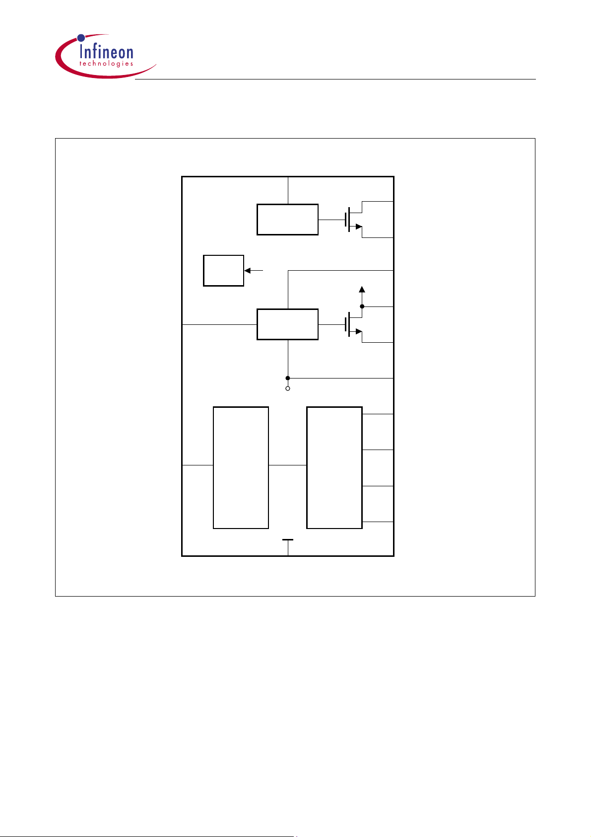
Block Diagram
TLE 6363 G
BOFB
12
Boost
Converter
14
13
TLE 6363
BOI
BOGND
BUC
R
6
1
Biasing
V
REF
Reference
Current
Generator
and
Oscillator
V
Boost
Converter
V
Internal
Buck
4
GND
Reset,
Window
Watchdog
and
System
Enable
10
9
8
7
5
3
2
11
BDS
V
BOOST
BUO
V
CC
SEN
WDI
RO
OVL
AEB03008
Figure 2
Block Diagram
Data Sheet V 1.1 4 2000-11-8
TLE 6363
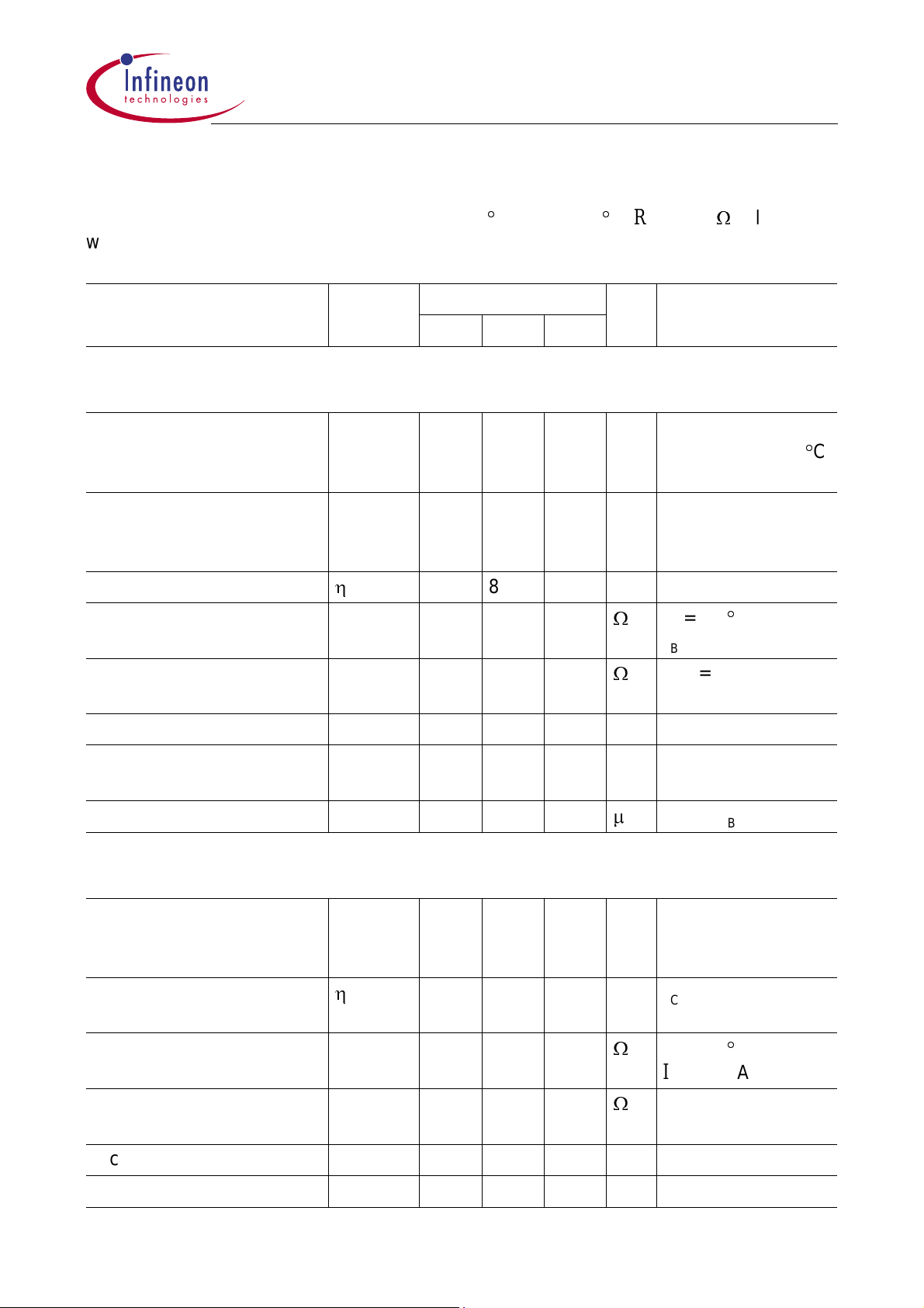
Absolute Maximum Ratings
Parameter Symbol Limit Val ues Unit Remarks
min. max.
Voltages
Boost input voltage
Boost o utput voltage
Boost feedback vol tage
Buck out put voltage
Buck driver supply voltage
Buck compensation input
voltage
Logic supply voltage
Reset output voltage
System Enable output
voltage
Current reference voltage
Watchdog input voltage
OVL output vol tage
V
BOI
V
BOOST
V
BOFB
V
BUO
V
BDS
V
BUC
V
CC
V
RO
V
SEN
V
R
V
WDI
V
OVL
–0.3 46 V –
–0.3 46 V –
–0.3 46 V –
–1 46 V –
–0.3 48 V –
–0.3 6.8 V –
–0.3 6.8 V –
–0.3 6.8 V –
–0.3 6.8 V –
–0.3 6.8 V –
–0.3 6.8 V –
–0.3 6.8 V –
ESD-Protection (Human Body Model ;
All pins to GND
V
HBM
R =1.5k
–2 2 kV –
τ
; C = 100 pF)
Temperatures
Junction temperature
Storage temperature
T
j
T
stg
–40 150
–50 150
C–
C–
Note: Stresses above those listed here may cause permanent damage to the dev ice.
Exposure to absolute maximum rating conditions for extended periods may affect
device reliability.
Data Sheet V 1.1 5 2000-11-8

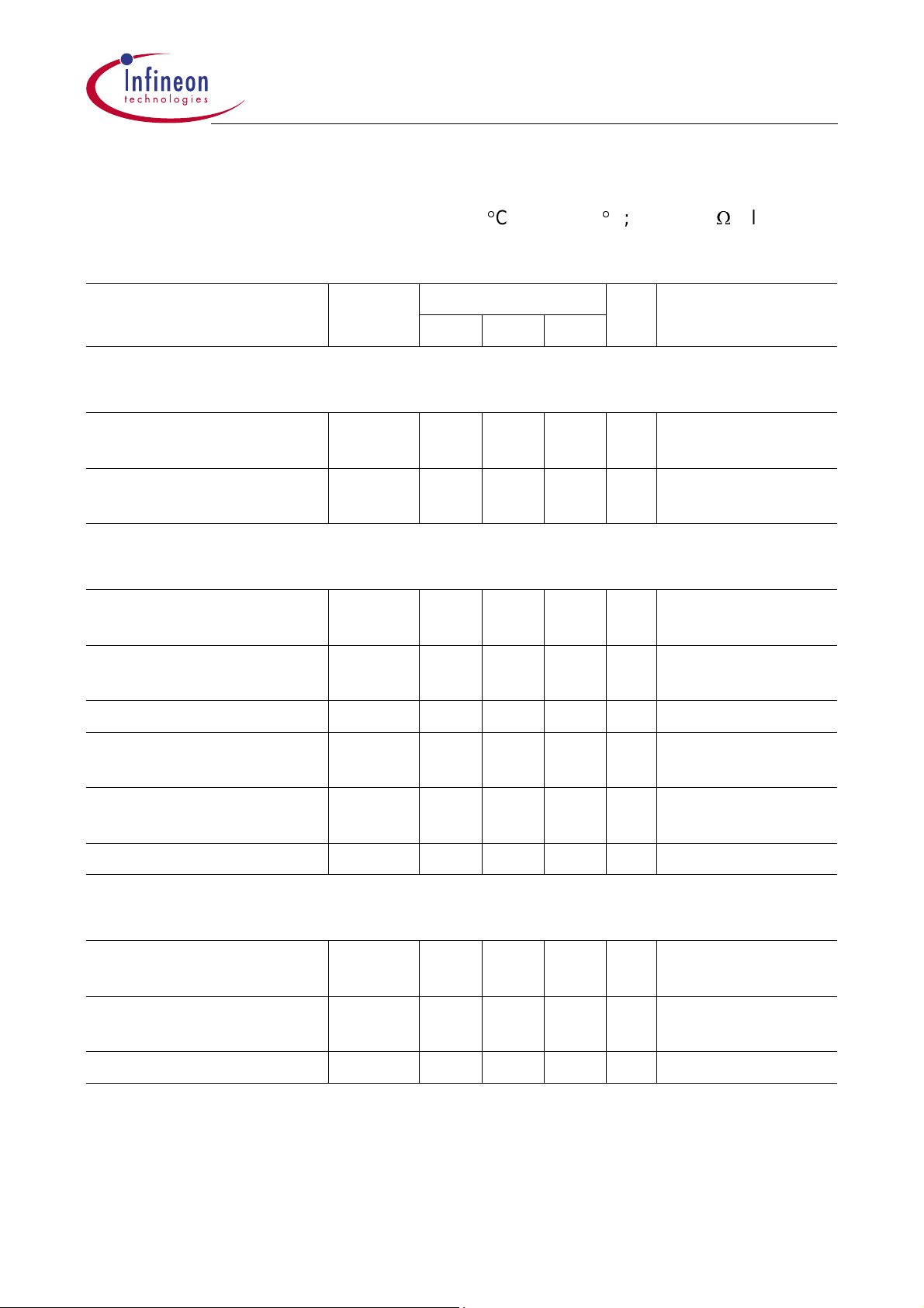
Operating Range
Parameter Symbol Limit Values Unit Remarks
min. max.
TLE 6363
Boost input voltage
Boost input voltage;
(normal operation)
Boost input voltage;
(normal operation)
Boost input voltage
Boost feedback vol tage
Buck out put voltage
Buck driver supply voltage
Buck compensation input
voltage
Logic supply voltage
Reset output voltage
System Enable output
voltage
V
BOI
V
BOOST
V
BOOST
V
BOOST
V
BOFB
V
BUO
V
BDS
V
BUC
V
CC
V
RO
V
SEN
–0.3 40 V –
535 VV
4.5 36 V V
BOOST
BOOST
increasing
decreasing
– 0.3 4.5 V Boost- and
Buck-Converter
OFF
03.0 V–
–0.6 40 V –
–0.3 48 V –
03.0 V–
4.00 6.25 V –
–0.3 VCC+0.3 V –
–0.3 VCC+0.3 V –
Watchdog input voltage
Current reference voltage
Junction temperature
V
V
T
WDI
R
j
0 VCC+0.3 V –
03.0 V–
–40 150
C–
Thermal Resistance
Junction ambient
R
thj-a
–120K/W–
Note: In the operating range, the functions given i n the circuit description are fulfilled.
Data Sheet V 1.1 6 2000-11-8
Electrical Characteristics
TLE 6363
8V<
V
<35V;4.75V<VCC<5.25V;–40C<Tj<150C; RR=47kτ; all voltages
Boost
with respect to ground; positive current defined flowing into pin; unless otherwise
specified.
Parameter Symbol Limit Values Unit Test Conditions
min. typ. max.
Current Consumption
Current consumption;
see application circuit
Current consumption;
see application circuit
Under- and Over-Voltage Lockout at
UV ON voltage;
I
Boost
I
Boost
V
BOUVON
–1.54mAICC=0mA;
I
BoLoad
=0mA
–510mAICC= 200 mA;
I
V
Boost
4.0 4.5 5.0 V V
BoLoad
BOOST
=50mA
increasing;
boost and buck conv. ON
UV OFF voltage;
V
BOUVOFF
3.5 4.0 4.5 V V
BOOST
decreasing
boost and buck conv. OFF
UV Hysteresis voltage
OV OFF voltage;
boost conv. OFF
OV ON voltage;
boost conv. ON
OV Hysteresis voltage
Over-Voltage Lockout at
OV OFF voltage;
buck conv. OFF
OV ON voltage;
buck conv. ON
OV Hysteresis voltage
V
V
V
V
V
CC
V
V
V
BOUVHY
BOOVOFF
BOOVON
BOUVHY
BUOVOFF
BUOVON
BUOVHY
0.2 0.5 1.0 V HY = ON - OFF
34 37 40 V V
30 33 36 V V
BOOST
BOOST
increasing
decreasing
1.5 4 10 V H Y = OFF - ON
5.5 6.0 6.5 V VCCincreasing
5.25 5.75 6.25 V VCCdecreasing
0.10 0.25 0.50 V HY = OFF - ON
Data Sheet V 1.1 7 2000-11-8
Electrical Characteristics (cont’d)
TLE 6363
8V<
V
<35V;4.75V<VCC<5.25V;–40C<Tj<150C; RR=47kτ; all voltages
Boost
with respect to ground; positive current defined flowing into pin; unless otherwise
specified.
Parameter Symbol Limit Values Unit Test Conditions
min. typ. max.
Boost-Converter; BOI, BOFB and V
Boost voltage;
V
BOOST
see application circuit
Boost Voltage;
V
BOOST
see application circuit
Efficiency; see. appl. circuit
Power-Stage ON
♣
R
BOON
resistance
BOOST
24.0 27.5 31.0 V 5 m A < I
100 mA;
8V<V
23 – 32 V 5 mA < I
100 mA;
8V<
–80–%I
– 0.6 0.75
τ
Boost
T
=25C;
j
I
BOI
Boost
T
j
<16V
Batt
Boost
V
<16V
Batt
= 100 mA
=1A
<
=25C
<
Power-Stage ON
R
BOON
––1.4
resistance
Boost overcurrent threshold
Feedback threshold voltage
Feedback input current
I
BOOC
V
BOFBTH
I
FB
1.0 1.3 1.8 A –
2.55 2.7 2.85 V V
–2 –0.4 0
Buck-Converter; BUO, BDS, BUC and V
Logic supply voltage V
Efficiency; see. appl. circuit
Power-Stage ON
♣
R
CC
BUON
4.9 – 5.1 V 1 mA < ICC<
–85– %ICC=250mA;
– 0.38 0.5
resistance
Power-Stage ON
R
BUON
––1.0
resistance
CC
τ
←
I
BOI
BOI
I
Boost
A2V<V
250 mA; see. appl.
circuit
V
Boost
τ
τ
T
=25C;
j
I
BUO
I
BUO
=1A
=12V
=25mA
BOFB
=25V
=1A
=1A
<4V
Buck overcurrent threshold
Input cur rent on pin
Data Sheet V 1.1 8 2000-11-8
V
CC
I
BUOC
I
CC
0.7 0.95 1.2 A –
–0.20.5mAVCC=5V
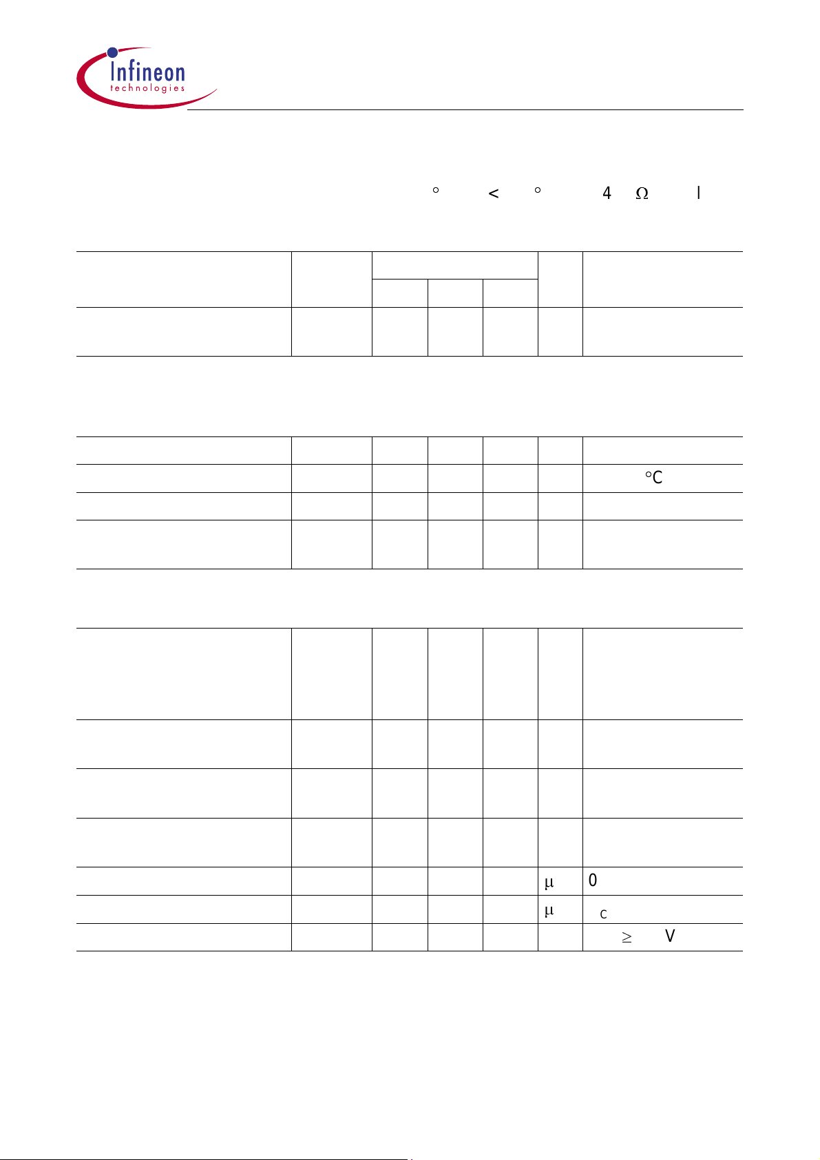
Electrical Characteristics (cont’d)
TLE 6363
8V<V
<35V;4.75V<VCC<5.25V;–40C<Tj<150C; RR=47kτ; all voltages
Boost
with respect to ground; positive current defined flowing into pin; unless otherwise
specified.
Parameter Symbol Limit Values Unit Test Conditions
min. typ. max.
Buck G a te supply voltage;
V
BGS
= V
BDS
– V
BOOST
V
BGS
5–10V–
Reference Input; R
(Oscillator; Timebase for Boost- and Buck-Converter, Reset and Watchdog)
Voltage on pin R
Oscillator frequency
Oscillator frequency
Cycle time for watchdog
V
f
OSC
f
OSC
t
CYL
R
1.3 1.4 1.5 V –
85 95 105 kHz Tj=25C
75 – 115 kHz –
–1.05–mst
CYL
= 100/f
OSC
and reset timing
Reset G enerator; R O
Reset threshold;
V
decreasing/increasing
CC
Reset low voltage
V
V
Reset low voltage V
Reset high voltage V
Reset pull up current
Reset Reaction time
I
t
Power-up reset delay time t
RT
ROL
ROL
ROH
RO
RR
RD
4.50 4.65 4.75 V VROHtoLorLtoH
transition;
V
remains low
RO
V
V
RT
CC
CC
>1V
< V
RT
RT
–0.20.4VI
–0.20.4VI
V
–
CC
0.1
– VCC+
0.1
– 240 –
50 100 150
–64–t
V I
←
A0V<VRO<4V
←
s VCC< V
CYL
down to
=2mA;
ROL
2.5 V <
=0.2mA;
ROL
1V<VCC< V
=0mA
ROH
V
∫
4.8 V
CC
Data Sheet V 1.1 9 2000-11-8

Electrical Characteristics (cont’d)
TLE 6363
8V<
V
<35V;4.75V<VCC<5.25V;–40C<Tj<150C; RR=47kτ; all voltages
Boost
with respect to ground; positive current defined flowing into pin; unless otherwise
specified.
Parameter Symbol Limit Values Unit Test Conditions
min. typ. max.
Watchdog Generator; WDI
H-input voltage threshold
L-input voltage threshold
Watchdog period
Start of reset;
V
V
T
t
SR
WDIH
WDIL
WD
––0.7
0.3
⌠
––V–
V
CC
V
CC
⌠
V–
– 128 – t
–64–t
CYL
CYL
V
V
CC
CC
∫
4.8 V
∫
4.8 V
after wat chdog time- out
Reset duration;
t
WDR
–64–t
CYL
V
CC
∫
4.8 V
after wat chdog time- out
Open window time
Closed wi ndow time
Window watchdog trigger
t
t
t
time
System Enable Output; SEN
Enable low voltage
V
Enable low voltage V
Enable high voltage V
Enable pull up current
I
OW
CW
WD
SENL
SENL
SENH
SEN
–32–t
–32–t
– 46.4 – t
CYL
CYL
CYL
–0.20.4VI
–0.20.4VI
V
–
CC
– VCC+
0.1
– 240 –
0.1
V I
←
A0V<V
V
∫
4.8 V
CC
V
∫
4.8 V
CC
V
∫
4.8 V
CC
=2mA;
SENL
V
2.5 V <
=0.2mA;
SENL
CC
< V
1V<VCC< V
=0mA
SENH
<4V
SEN
RT
RT
Data Sheet V 1.1 10 2000-11-8

Electrical Characteristics (cont’d)
TLE 6363
8V<
V
<35V;4.75V<VCC<5.25V;–40C<Tj<150C; RR=47kτ; all voltages
Boost
with respect to ground; positive current defined flowing into pin; unless otherwise
specified.
Parameter Symbol Limit Values Unit Test Conditions
min. typ. max.
Boost Status Output; OVL
Enable low voltage
Boost feedback threshold
voltage;
V
OVLL
V
OVLTH
–0.20.4VI
2.5 V <
OVLL
=1mA;
V
< V
CC
2.3 2.45 2.6 V See application
circuit
RT
Thermal Shutdown (Boost and Buck-Converter OFF)
Thermal shutdown junction
T
jSD
150 175 200
C–
temperature
Thermal switch-on junc tion
T
jSO
120 – 170
C–
temperature
α
Temperature hysteresis
T –30–K–
Note: The listed characteristics are ensured over the operating range of the integrated
circuit. Typical characteristics specify mean values expected over the production
T
spread. If not otherwise specified, typical characteristics apply at
=25C and
A
the given supply voltage.
Data Sheet V 1.1 11 2000-11-8

TLE 6363
Circuit Des cription
Below some important sections of the TLE 6363 are described in more detail.
Power On Reset
In order to avoid any system failure, a sequence of several conditions has to be passed.
V
In case of
pin RO to reset an external microcontroller. When the level of
threshold
beforeswitchingtoHIGH.IfVCCdrops below the reset threshold VRTfor a time extending
the reset reaction time
period
t
RD
“glitches” on the
power down (VCC< VRTfor t > tRR) a logic LOW signal is generated at the
CC
V
reaches the reset
CC
V
, the signal at RO remains LOW for the Power-up reset delay time t
RT
t
, the reset circuit is activated and a power down sequence of
RR
RD
is initiated. The reset reaction time tRRavoids wrong t riggering caused by short
V
-line.
CC
<
t
V
CC
typ. 4.65 V
V
RT
1 V
Start-Up ON Delay
RO
H
L
t
RD
Power Start-Up Normal Failed N Failed Normal
RR
t
RR
ON Delay
Started
InvalidInvalid
<
t
RD
ON Delay
Stopped
Invalid
Figure 3 Reset Function
t
RD
t
t
AET02950
Data Sheet V 1.1 12 2000-11-8

TLE 6363
Watchdog Operation
The watchdog uses one hundr ed of the oscillator’s clock signal period as a timebase,
t
defined as the watchdog cycle time
After power-on, t he reset output si gnal at the RO pin (microcontroller r eset) is kept LOW
t
for the reset delay time
, i.e. 64 cycles. With the LOW to HIGH transition of the signal
RD
at RO the device starts the closed window time
this window is interpreted as a pretrigger failure according to the figures shown below.
After the closed window the open window with the duration
window lasts at minimum until the trigger process has occurred, at maximum
32 cycles.
A HIGH to LOW transition of the watchdog trigger signal on pin WDI is taken by a trigger.
To avoid wrong triggering due to par asitic glitches two H IGH samples followed by two
LOW samples (sample period
t
CYL
appears at the watchdog input pin WDI during the open window or a power up/down
occurs, the watchdog window signal is reset and a new closed window fo llows.
A reset is generated (RO goes LOW) if there is no trigger pulse during the open wi ndow
or if a pretrigger occurs during the closed wi ndow. This reset happens after 64 cycles
after the latest valid closed window start time and lasts for further 64 cycles.
Thetriggering is correct also, if thefirst three samples (two HIGH one LOW) of the trigger
pulse at pin WDI are inside the closed window and only the fourth sample (the second
LOW sample) is taken in the open window.
In addit ion to the microcontroller reset signal RO the device generates a system enable
signal at pin SEN. If RO is HIGH the system enable goes active HIGH with the first valid
watchdog trigger pulse at pin WDI. The SEN output goes LOW imm ediately if a
pretrigger, a missing trigger or a power down reset occurs.
.
CYL
t
= 32 cycles. A trigger signal within
CW
t
is started. The open
OW
t
is
OW
) are decoded as a valid trigger. If a trigger signal
Data Sheet V 1.1 13 2000-11-8

t
CW
= 32 x
t
= 64 x
SR CYL
t
CYL
TLE 6363
128 x
T
=
WD
t
t
= 32 x
OW
t
CYL
t
CYL
t
WDR
= 64 x
t
CYL
Definition
Definition
Worst Case
f
=
OSCfOSCmax
f
f
=
OSC OSCmin
Closed window
WDI
Closed Window
Reset start delay time after window
watchdog time-out
t
CW+OWmin
t
CWmax CW
t
= (t+ )(1 - )
CW
=
(1 +
t
t
*
WD
Open window
Open Window
t
ECW
OW
)
∆
∆
t
OWmin
Watchdog
trigger signal
Valid
Reset duration time after window
watchdog time-out
t
= end of open window
EOW
Example with:
t
= 1 ms
CYL
∆
= 10% (oscillator deviation)
results to:
t
OWmin
= 32 ms - 0.1 x (32 ms + 64 ms)
t
OWmin
= 22.4 ms
t
OWmin
*
recommended watchdog trigger time
Open window Closed window
AET02951
WDI
WDI
t
ECW
= Watchdog decoder sample point
Indifferent
Not valid
t
EOW
AET02952
Figure 4 Wi ndow Watchdog Definitions
Data Sheet V 1.1 14 2000-11-8

a) Perfect Triggering after Power on Reset
V
CC
V
RT
TLE 6363
RO
WDWI
WDI
SEN
System Failed System Enable System Failed
b) Incorrect Triggering
t
WDR
= 64 Cycles
t
SR
RO
= 128 Cycles
T
WD
WDWI
t
= 64 Cycles
RD
= 64 Cycles
32 Cycles
CW OW CW OW CW CW
32 Cycles
= 64 Cycles
t
SR
xx
xx
t
1
xx
xx
xx
t
xx
t
2
3
t
t
t
t
t
t
CW OW CW OW CW CW
OW
OW
t
WDI
SEN
1)
Pretrigger
2)
Incorrect trigger duration within watchdog
open window OW:
3)
Incorrect trigger duration within watchdog
open window OW:
4)
Missing trigger
xx
xxx
xxxxx
1) 2) 3)
t
HIGH
t
LOW
32 Cycles
< 2 Cycles
< 2 Cycles
x
x
Legend: WDWI= Internal Watchdog Window
xx
xx
4)
OW = Open Window (trigger signal at WDI)
= Closed Window (trigger signal at WDI)CW
x = Sample Point
t
t
AED02945
Figure 5 Wi ndow Watchdog Function
Data Sheet V 1.1 15 2000-11-8

TLE 6363
Boost Converter
The TLE 6363 contains a fully integr ated boost converter (except the boost-diode),
which provides a supply voltage for an energy reserve e.g. an airbag f iring system. The
regulated boost output voltage
V
BOOST
resistors) providing the feedback voltage for the boost feedback pin BOFB. Th e energy
which is stored in the external electrolytic capacitor at
airbag firing, even if the battery is disconnected by a car crash.
L
The boost inductanc e
(typ. 100←H) is PWM-switched by an i n tegrated current
BO
limited power DMOS transistor with a programmable (external resistor
An internal bandgap reference provides a temperature independent, on chip trimmed
reference voltage for the regulation loop. An error amplifier compares the reference
voltage with the boost feedback signal
(determination of the output boost voltage V
Application note for programming the output voltage at pin
is programmable by a divider network (external
V
BOFB
BOOST
V
BOOST
from the external divider network
).
V
BOOST
guarantees accurate
R
) frequency.
R
:
V
BOOST
=
V
BOFBTH
With a PWM (P
R
ΕΦ
BO1
------------------------------------ -
⌠
ulse Width Modulation) comparator the output of the error amplifier is
R
+
BO2
R
BO2
compared to a periodic linear ramp, provided by a sawtooth signal of the oscillator
connected to pin R. A logic signal with variable pulse width is genera ted. It passes
through the logic circuits (sets the output latch PWM-FF) and driver circuits to the power
switching DMOS. The Schmitt-trigger output resets the output flip-flop PWM-FF by
NOR 2. The PWM signal is gated by the NAND 2 to guarantee a dominant reset.
Data Sheet V 1.1 16 2000-11-8

V
Boost
V
10
BOFB
Pin 12
2.8 V
R
Pin 1
V
thUV
4 V
µ
REF
GND
GND
I
A
GND
=
=
Pullup
=
OV
COMP
V
thOV
38 V
UV
COMP
Error
AMP
+
+
-
+
-
L when
V
OV at
Boost
L when
T
> 175 ˚C
j
H when
V
Boost
H when
Overcurrent
Oscillator
V
max
V
min
< 4 V
NAND 3
&
tfrtrt
H when
T
> 175 ˚C
j
or OV at
NOR 1
1
t
V
Boost
L when
Error
NAND1
&
Schmitt-trigger 1
V
Ramp
V
high
low
Error-FF
R
&
&
S
Error-Signal
Error-Ramp
trtrft
Q
Q
t
Error
Gate
NOR 2
H when
Error
1
NAND 2
&
PWM
COMP
Clock
H when Outputcurrent > 1.2 A
+
H when
Error-Signal
<
Error-Ramp
Unlock
Detector
PWM-FF
R
&
&
S
TLE 6363
BOI
Pin 14
INV
H =
Q
OFF
Q
1
OC
COMP
H =
ON
+
Gate
Driver
=
V
thOC
18 mV
Boost Status
Low if Battery
Disconnected
Power
D-MOS
R
Sense
14.5 m
BOGND
Pin 13
OVL
Pin 11
GND
AEB02946
Ω
Figure 6 Boost Converter Block Diagram
Figure 7 shows the m ost important w aveforms during operation; for low, medium and
high loads up to overload condition. The output transistor is switched off immediately if
the overcurrent comparator detects an overcurrent level at the power DMOS or if the
sense output switches to low induced by a
V
BOOST
undervoltage command.
The TLE 6363 is also protected against several boost loop errors:
I
In case of a feedback interruption a pull up current source (
typ. 0.4←A), integrated at
FB
pin BOFB pulls the voltage at the feedback pin BOFB above the reference voltage. The
boost output is switched off by the high error voltage which controls the
PWM-Comparator at a zero duty cycle.
In the case of a resistive loop error caused by leakage currents to ground, the boost
output voltage would increase to very high values. In order to protect the
V
BOOST
input as
well as the external load against catastrophic failures, an overvoltage protection is
provided which switches the output transistor off as soon as the voltage at pin
exceeds the inte rnal fixed overvoltage threshold V
BOOVOFF
= typ. 37 V.
V
BOOST
Data Sheet V 1.1 17 2000-11-8

Application Note:
TLE 6363
A short circuit from
V
BOOST
to ground will not destroy t he IC, however, it may damage the
external boost diode or the boost inductance if there is no overcurrent limitation in that
path.
V
C
and
V
Error
V
CP
V
CV
OCLK
PWM
I
BOI
I
BOLI
H
L
H
L
Error Voltage
t
t
t
I
DBO
V
BOI
V
BOOST
V
S
Overcurrent Threshold Exceeded
Controlled by theLoad-Current Increasing with Time;
Overcurrent CompControlled by the Error Amp
AED02672
Figure 7 Most Important Waveforms of the Boost Converter Circuit
t
t
t
Data Sheet V 1.1 18 2000-11-8

TLE 6363
Buck Converter
A stabilized logic supply voltage (typ. 5 V) for general purpose is realized in the system
L
by a buck converter. An external buck-inductance
DMOS power transistor with the programmed frequency (pin R).
is PWM switched by a high side
BU
The buck regulator supply is given by the boost converter output
V
BOOST
,incaseofa
battery power-down the stored energy of the boost converter capacitor is used.
Like t he boost converter, the buck converter uses the tem perature compensated
bandgap reference voltage (typ. 2.8 V) for its regulation loop.
This reference voltage is connected to the non-inverting input of the error amplifier and
an internal voltage divider supplies the inverting input. There for e the output voltage
V
CC
is fixed due to th e internal resistor ratio to typ. 5.0 V.
The output of the error amplifie r goes to the inverting input of the PWM compar ator as
well as to the buck compensation output BUC.
When the error amplifier output voltage exceeds the sawtooth voltage the output power
MOS-transistor is switched o n. So the duration of the output transistor conduction phase
V
depends on the
level. A logic signal PWM with variable pulse width is generated.
CC
Data Sheet V 1.1 19 2000-11-8

TLE 6363
V
CC
R
BUC
Pin 6
V
CC
Pin 7
R
Pin 1
R
R
Prot1
Ω
200
V
CC
VCC1
Ω
22
VCC2
Ω
28
GND
Oscillator Schmitt-trigger 1
V
max
V
min
=
GND
rttftr
Error
AMP
V
REF
2.8 V
Error-
-
Signal
+
ErrorRamp
Ramp
t
R
39.7
R
10.3
PWM
COMP
V
high
V
low
VCC3
VCC4
+
Ω
Ω
GND
t trft
=
V
1.2 V
GND
H when
Error-Signal
<
Error-Ramp
L when
T
> 175 ˚C
j
r
t
OV
COMP
+
-
thOV
Clock
H when
V
OV at
L when
Overcurrent
Output Stage
OFF when H
Error-FF
R
&
&
S
CC
Q
OFF when H
Q
H when
UV at
NOR 1
V
1
Boost
UV
COMP
NAND 2
&
+
=
GND
V
thUV
4 V
PWM-FF
R
S
L when
Overcurrent
&
Q
&
Q
OC
COMP
+
INV
H = H =
1
OFF
ON
V
thOC
18 mV
Boost
Driver
Supply
Gate
Driver
V
=
Boost
Pin 9
R
Sense
18 m
Ω
BDS
Pin 10
Power
D-MOS
BUO
Pin 8
AEB02947
Figure 8 Buck Converter Block Diagram
External loop compensation is required for converter stability, and is formed by
connecting a compensation resistor-capacitor series-network (
R
BUC
, C
) between pin
BUC
BUC and GND.
V
In the case of overload or short-circuit at
overcurrent threshold I
) the DMOS output transistor is switched off by the
BUOC
(the output current exceeds the buck
CC
overcurrent comparator immediately. The pulse width is then controlled by the
overcurrent comparator as seen before in the boost description.
V
In order to protect the
input as well as the external load against catastrophic failures,
CC
an overvoltage protection is provided whi ch switches the output transistor off as soon as
the voltage at pin
exceeds the internal fix ed overvoltage threshold V
CC
BUOVOFF
= typ.
V
6.0 V.
Data Sheet V 1.1 20 2000-11-8

V
V
C
and
Error
V
CP
V
CV
TLE 6363
Error Voltage
OCLK
PWM
I
BUO
I
BULI
I
DBU
V
BUO
V
BOOST
V
CC5
t
H
L
t
H
L
t
t
t
t
Overcurrent Threshold Exceeded
Controlled by theLoad-Current Increasing with Time;
Overcurrent CompControlled by the Error Amp
AED02673
Figure 9 Most Important Waveforms of the Buck Converter Circuit
Data Sheet V 1.1 21 2000-11-8

TLE 6363
Application Circuit
Figure 10 shows the application circuit of the TLE 6363 with the suggested external
parts.
L
BO
100 µH
C
S
220 nF
D
BO
C
BO1
10 nF
R
BO1
100 k
C
Ω
BO1
4700 µF
R
BO2
10 k
BOI
14
BOGND
13
10 BDS
V
BOOST
89BUO
V
7
CC
C
BOT
10 nF
L
BU
220 µH
D
BU
Ω
C
BU1
100 µF
5 SEN
WDI3
11
RO2
OVL
10 k
Ω
Device Type Supplier Remarks
D
1
D
2
D
BO
D
BO
D
BU
L
BO
L
BO
L
BU
L
BU
BAW78C
BAW78C
BAW78B
B82442-A1104
B82442-H2204
Do3316P-224
Infineon
Infineon
Infineon
EPCOS
CoilcraftDo3316P-104
EPCOS
Coilcraft
200 V; 1 A; SOT-89
200 V; 1 A; SOT-89
100 V; 1 A; SOT-89
Schottky; 40 V; 1 AmultipleSS14
Schottky; 100 V; 1 A
100 µH; 0.25 A; 1.28
100 µH; 1.2 A; 0.28
220 µH; 0.24 A; 2.72
220 µH; 0.8 A; 0.61
C
BO2
220 nF
C
BU2
220 nF
I
V
V
System
Enable
Output
Watchdog
Trigger
Output
Reset
Output
Boost
Status
Output
Ω
Ω
Ω
Ω
BOLoad
BOOST
CC
AEB03007
V
Batt
BUC 6
R
BUC
47 k
C
BUC
470
nF
R
R
47 k
D
1
TLE 6363 G
Biasing
Ω
1R
Ω
C
L
10 µF
V
REF
V
Reference
Current
Generator
and
Oscillator
Boost
Converter
V
Boost
Buck
Converter
Internal
4
D
2
ZD1
36 V
BOFB
12
Reset
Window
Watchdog
and
System
Enable
GND
Figure 10 Application Circuit
Data Sheet V 1.1 22 2000-11-8

TLE 6363
Diagrams: Oscillator and Boost/Buck-Converter Performance
In the following the behaviour of the Boost/Buck-converter and the oscillator is shown.
Oscillator Frequency D eviation vs.
Junction Temperature
OSC
AED02938
T
j
10
kHz
∆
f
OSC
5
Referred to f
T
= 25 ˚C
at
j
0
-5
-10
-15
-50 -25 0 25 50 75 100 ˚C 150
Boost Feedback Cu rrent vs.
Junction Temperature
-200
nA
I
FB
-300
-400
-500
-600
-700
-50 -25 0 25 50 75 100 ˚C 150
AED02939
T
j
Data Sheet V 1.1 23 2000-11-8

TLE 6363
Current Consumption vs.
Junction Temperature
3
mA
I
Boost
2.5
Boost ON
Buck ON
2
I
I
1.5
1
0.5
-50 -25 0 25 50 75 100 ˚C 150
BO boost
= 0 mA
CC
= 0 mA
AED02940
T
j
Efficiency Buck vs.
Boost Voltage
95
%
η
90
85
80
75
70
65
5
15 25 V 30
V
I
CC
Load
AED02941
= 5 V
= 120 mA
80 mA
40 mA
V
Boost
Efficiency Buck vs.
Load
90
%
η
85
RT, HT
80
75
70
65
50 150 250mA
CT
AED02942
I
LOAD
Data Sheet V 1.1 24 2000-11-8

TLE 6363
Efficiency Boost vs.
Input Voltage
95
I
%
η
90
85
RT
80
75
70
8
Boost
10 12 14 16
= 60 mA
HT
CT
AED02943
V
V
Batt
Boost Output Voltage vs.
Load
31
V
V
Boost
30
RT
29
28
27
26
20
40 60 80 100
HT
CT
AED02944
mA
I
LOAD
Oscillator Frequency vs. Resistor
from R to GND
AED02982
Ω
R
R
f
OSC
1000
kHz
500
200
100
50
20
10
T
= 25 ˚C@
j
5
10 20 50 100 200 k 1000
Boost and Logic Output Voltage vs.
Junction Temperature
AED02983
T
j
V
Boost
V
CC
5.025
5.000
4.975
4.950
30
V
29
I
= 50 mA
28
Boost
27
26
V
= 250 mA
I
CC
-50
-25 0 25 50 75 100 ˚C 150
Data Sheet V 1.1 25 2000-11-8

TLE 6363
Boost and Buck ON Resistance vs.
Junction Temperature
BUO
AED02984
= 1 A
T
j
R
1000
m
ON
800
700
600
500
400
300
200
100
Ω
= 1 A
R
BOON
0
-50
-25 0 25 50 75 100 ˚C 150
I
@
BOI
RI
@
BUON
Boost and Buck Overcurrent Threshold
vs. Junction Temperature
1.4
A
I
OC
1.3
I
(Boost-Converter)
BOOC
1.2
1.1
I
1
(Buck-Converter)
BUOC
0.9
0.8
-50
-25 0 25 50 75 100 ˚C 150
AED02985
T
j
Data Sheet V 1.1 26 2000-11-8

Package Outlines
P-DSO-14-2
(Plastic Dual Small Outline Package)
TLE 6363
Sorts of Packing
Package outlines for tubes, trays etc. are contained in our
Data Book “Package Information”
SMD = Surface Mounted Device
GPS05474
Dimensions in mm
Data Sheet V 1.1 27 2000-11-8

Edition 2000-11-8
PublishedbyInfineon Technologies AG,
St.-Martin-Strasse53,
D-81541München,Germany
©InfineonTechnologiesAG2000.
All Rights Reserved.
Attention please!
Theinformation hereinisgivento describe
certain components and shall not be considered as warranted characteristics.
Termsof delivery andrightsto technical
changereserved.
We hereby disclaim any and all warranties,
includingbut notlimitedto warrantiesof
non-infringement, regardingcircuits,descriptions and charts stated herein.
InfineonTechnologies is an approvedCECC
manufacturer.
TLE 6363
Information
For further information on technology, delivery terms and conditions and prices please
contactyournearestInfineonTechnologies
Officein Germany orour Infineon TechnologiesRepresentativesworldwide (see addresslist).
Warnings
Due to technical requirementscomponents
may contain dangerous substances. For information on the types in question please
contactyournearestInfineonTechnologies
Office.
Infineon TechnologiesComponents mayonly
be used in life-supportdevices orsystems
with the express written approval of Infineon
Technologies,ifafailureof such components
canreasonablybe expectedtocausethe failureofthatlife-supportdeviceorsystem,or to
affect the safety or effectiveness of that deviceor system.Life support devices or systems are intended to be implanted in the human body,or to support and/or maintain and
sustainand/orprotecthumanlife.Iftheyfail,it
isreasonable toassume thatthehealthof the
useror otherpersonsmay be endangered.
Data Sheet V 1.1 28 2000-11-8
 Loading...