

现货库存、技术资料、百科信息、热点资讯,精彩尽在鼎好!
LIN-Transceiver LDO TLE 6285
Target Data Sheet
1Overview
1.1 Features
• Single-wire transceiver, suitable for LIN protocol
• Transmission rate up to 20 kBaud
• Compatible to LIN specification
• Compatible to ISO 9141 functions
• Very low current consumption in sleep mode
• Control output for voltage regulator
• Short circuit proof to ground and battery
• Overtemperature protection
• Output voltage 5V, tolerance £ ± 2 %
• 150 mA output current capability
• Low-drop voltage
• Overtemperature protection
• Reverse polarity protection
• Short-circuit proof
• Adjustable reset threshold
• Wide temperature range
• Suitable for use in automotive electronics
P-DSO-16-4
Type Ordering Code Package
TLE 6285 G on request P-DSO-16-4
1.2 Description
The TLE 6285 is a single-wire transceiver with a LDO. It is chip by chip integrated circuit
in a P-DSO-16-4 package. It works as an interface between the protocol controller and
the physical bus. The TLE 6285 is especially suitable to drive the bus line in LIN systems
in automotive and industrial applications. Further it can be used in standard ISO9141
systems.
In order to reduce the current consumption the TLE 6285 offers a sleep operation mode.
In this mode a voltage regulator can be controlled in order to minimize the current
consumption of the whole application (VR in sleep mode <1µA!). The on-chip voltage
regulator (VR) is designed for this application but it is also possible to use an external
Version 1.02 1 2002-05-15

Target Data TLE 6285
voltage regulator. A wake-up caused by a message on the bus enables the voltage
regulator and sets the RxD output low until the device is switched to normal operation
mode. To achieve proper operation of the µC, the device supplies a reset signal. The
reset delay time is selected application specific by an external capacitor. The reset
threshold is adjustable.
®
The IC is based on the Smart Power Technology SPT
which allows bipolar and CMOS
control circuitry in accordance with DMOS power devices existing on the same
monolithic circuit.
The TLE 6285 is designed to withstand the severe conditions of automotive applications.
Version 1.02 2 2002-05-15
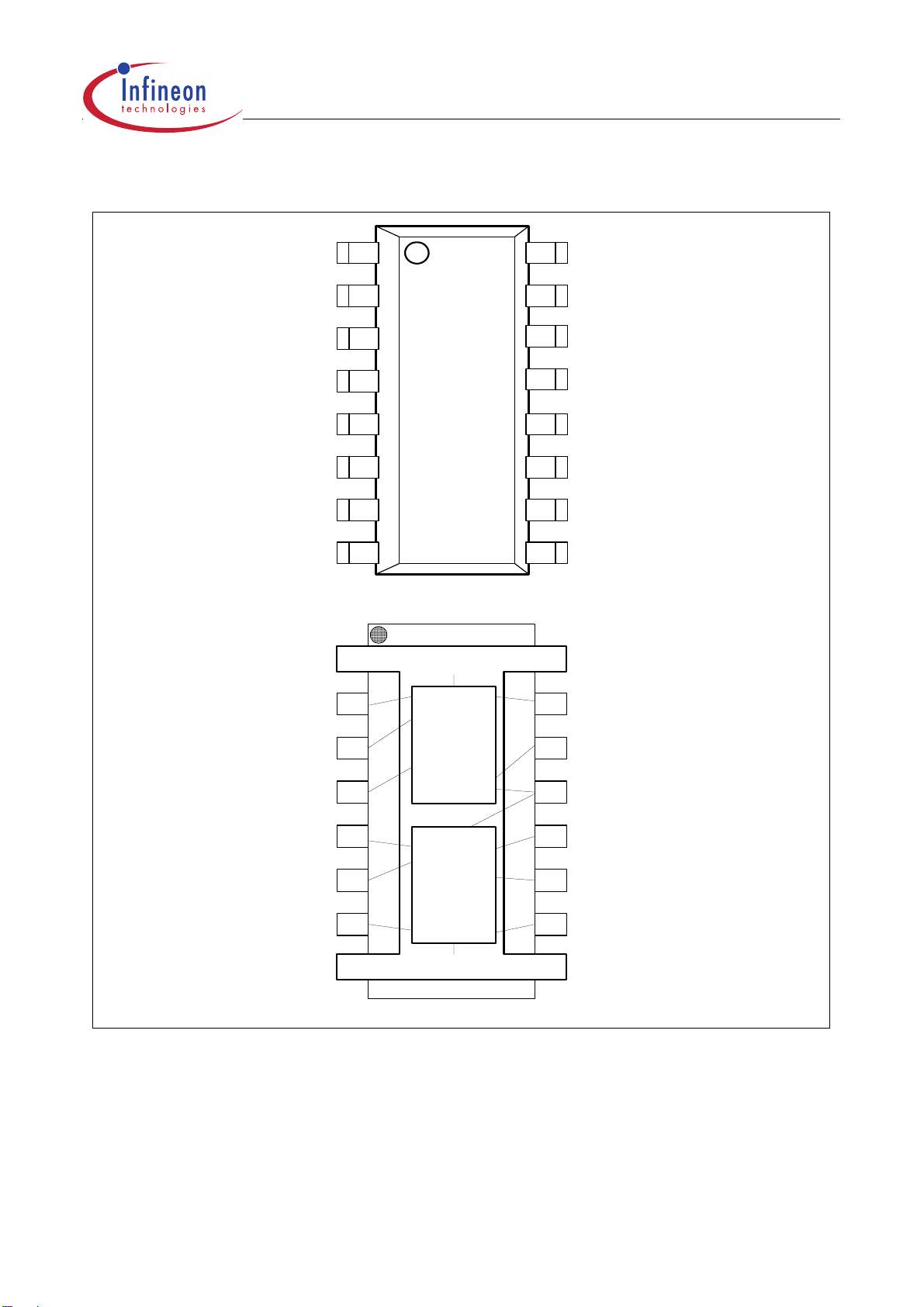
1.3 Pin Configuration (top view)
Target Data TLE 6285
GND
INHI
RO
V
CCO
INHO
RxD
ENLIN
GND
GND
1
2
3
4
5
6
7
89
P-DSO-16-4
116
Leadframe
16
15
14
13
12
11
10
GND
RD
R
Th
V
BAT
BUS
TxD
V
CCI
GND
GND
Figure 1 Pinout
INHI
RO
V
CCO
INHO
RxD
ENLIN
GND
2
Chip:
Voltage
Regulator
4
5
6
7 10
8
Chip:
Transceiver
P-DSO-16-4
15
RD
143
R
Th
13
V
BAT
12
BUS
11
TxD
V
CCI
9
GND
Version 1.02 3 2002-05-15
Target Data TLE 6285
1.4 Pin Definitions and Functions:
Pin No. Symbol Function
1,8,9,16 GND Ground; place to cooling tabs to improve thermal behavior
2 INHI Inhibit Voltage Regulator Input; TTL compatible, HIGH active
(HIGH switches the VR on); connect to V
if not needed
BAT
3ROReset Output; open collector output connected to the output via
a resistor of 20kW
4V
CCO
5V Output; connected to GND with 22µF capacitor, ESC<3W
5 INHO Inhibit LIN Output; to control a voltage regulator
6RxDReceive Data Output; internal 30kW pull up to Vs, LOW in
dominat state
7ENLINEnable LIN Input; integrated 30kW pull down, transceiver in
normal operation mode when HIGH
10 V
CCI
5V Supply Input; VCC input to supply the LIN transceiver
11 TxD Transmit Data Input; internal 30kW pull up to Vs, LOW in
dominant state
12 BUS LIN BUS Output/Input; internal 30kW pull up to Vs, LOW in
dominant state
13 V
BAT
Battery Supply Input; a reverse current protection diode is
required, block GND with 100nF ceramic capacitor and 22µF
capacitor
14 R
Th
Reset Threshold; internal defined typical 4.6V, adjustable down
to 3.5V according to the voltage level on this pin; connect to GND
if not needed
15 RD Reset delay; connected to ground via external delay capacitor
Version 1.02 4 2002-05-15
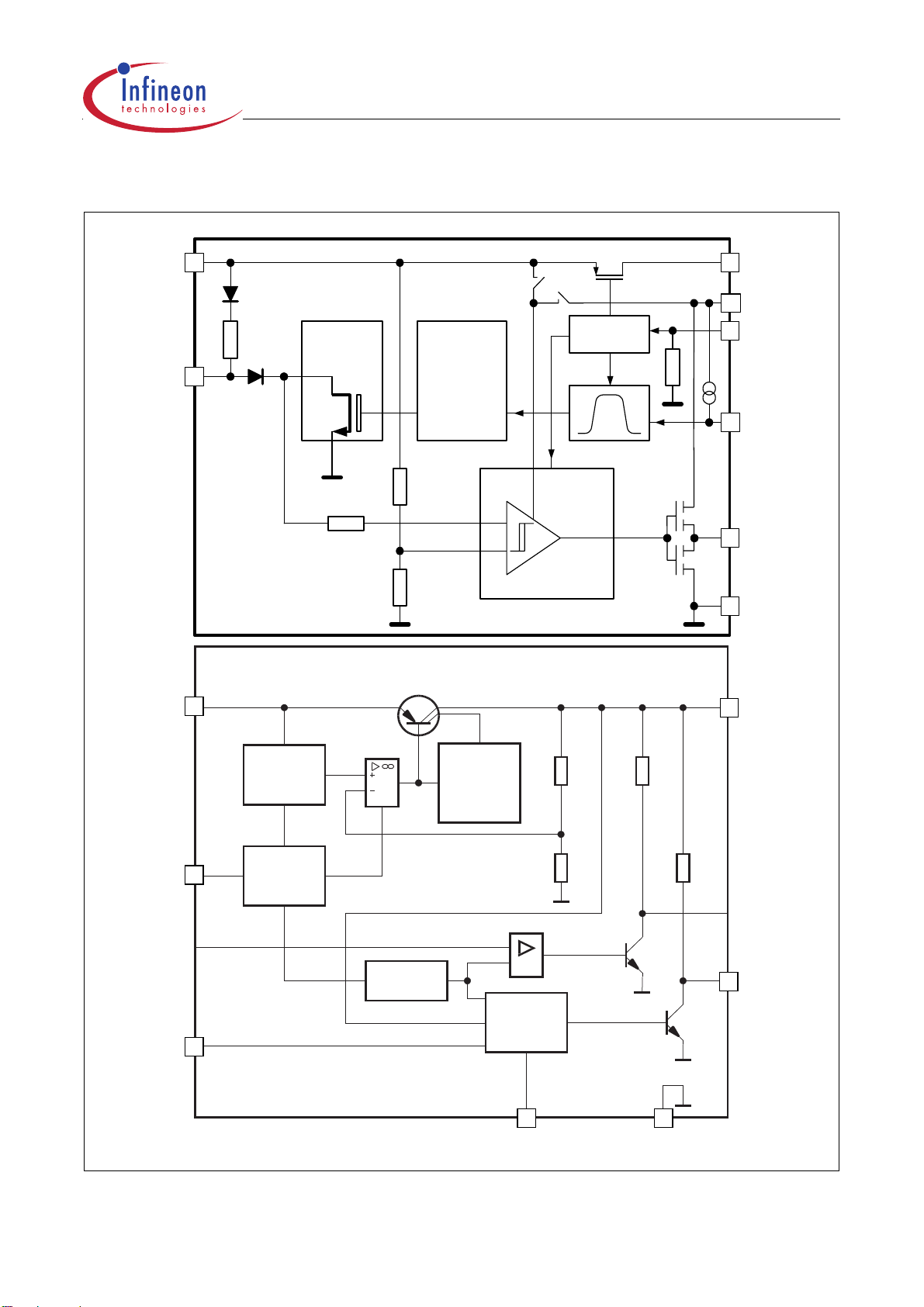
1.5 Functional Block Diagram
Target Data TLE 6285
V
Bus
BAT
13
30 k
9
12
Output
Stage
Driver
Mode
Control
30 k
9
5
10
7
INHO
V
CCI
ENLIN
Temp.-
Protection
11
TxD
Receiver
6
RxD
TLE 6259 G
TLE 4299
13
V
I
Bat
4
5
GND
V
Q
CCO
Band-
Gap-
Reference
INHI
INH
2
Inhibit
Control
SI
R
14
RADJ
Th
Figure 2 Block Diagram
Reference
Current
and
Saturation
Control
Reset
Control
15
D
RD
1,8,9,16
R
SO
GND
GND
R
RO
3
AEB03104
SO
RO
RO
Version 1.02 5 2002-05-15
Target Data TLE 6285
p
2 Circuit Description
The TLE 6285 is a single-wire transceiver combined with a LDO. It is a chip by chip
integrated circuit in a P-DSO-16-4 package. It works as an interface between the
protocol controller and the physical bus. The TLE 6285 is especially suitable to drive the
bus line in LIN systems in automotive and industrial applications. Further it can be used
in standard ISO9141 systems. The on-chip voltage regulator with watchdog is designed
for sleep mode applications but it is also possible to use an external voltage regulator.
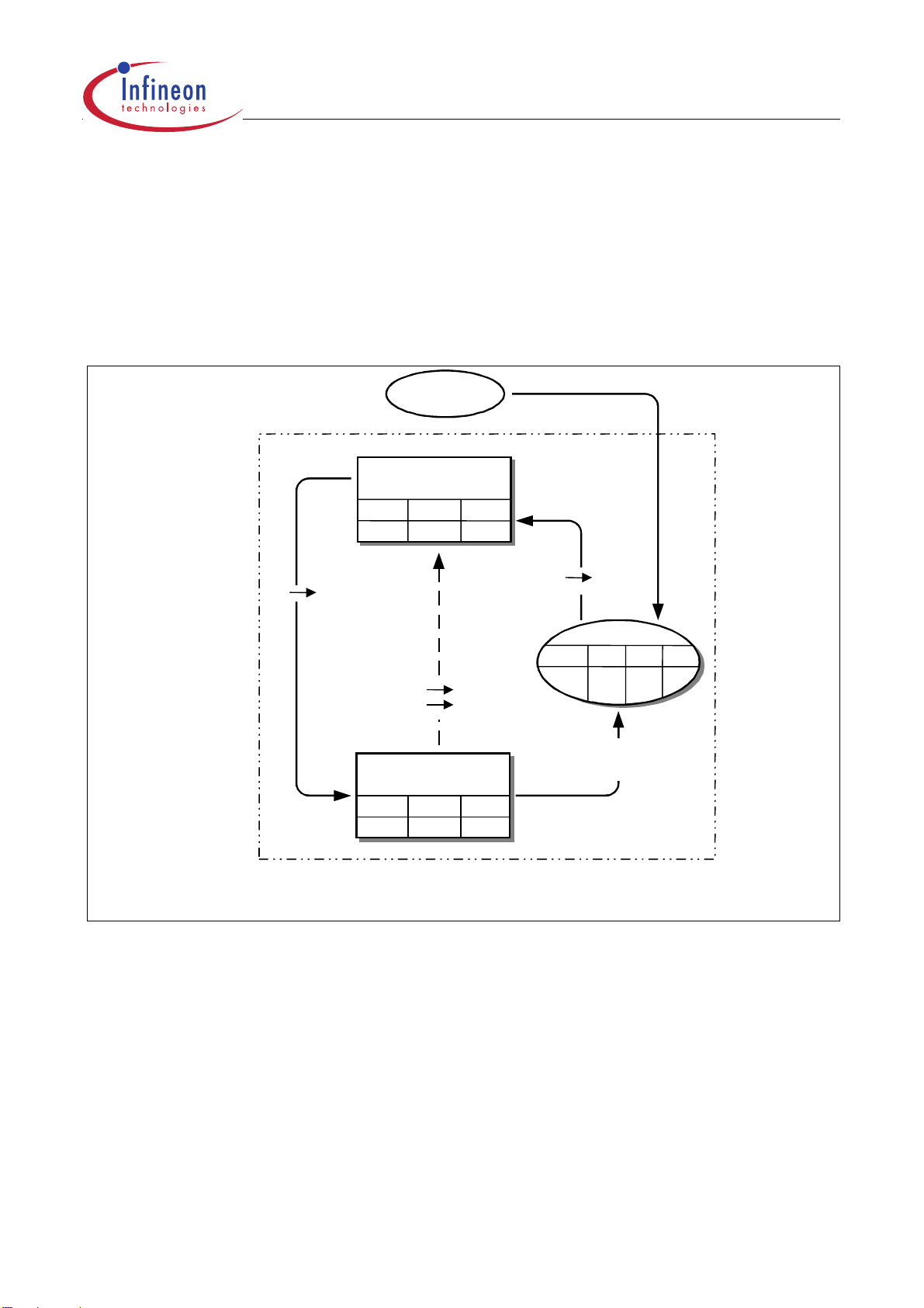
Start Up
Power Up
Normal Mode
ENLIN
INHO
high high
ENLIN
low
ENLIN
(V
CC
Sleep Mode
ENLIN
INHO
low floating
1)
after wake-up via bus
2)
ON when INHO not connected to INHI
3)
after start u
Figure 3 Operation Mode State Diagram
V
CC
ON
high
ON)
V
CC
OFF
2)
ENLIN high
Stand-By
INHO
ENLIN
low high
Wake Up
t > t
WAKE
RxD
low
high
V
CC
1)
ON
3)
2.1 Operation Modes
In order to reduce the current consumption the TLE 6285 offers a sleep operation mode.
This mode is selected by switching the enable input EN low (see figure 3, state
diagram). In the sleep mode a voltage regulator can be controlled via the INHO output
in order to minimize the current consumption of the whole application. A wake-up caused
by a message on the communication bus automatically enables the voltage regulator by
switching the INHO output high. In parallel the wake-up is indicated by setting the RxD
output low. When entering the normal mode this wake-up flag is reset and the RxD
output is released to transmit the bus data.
Version 1.02 6 2002-05-15

Target Data TLE 6285
In case the voltage regulator control input is not connected to INH output or the
microcontroller is active respectively, the TLE6285 can be set in normal operation mode
without a wake-up via the communication bus.
2.2 LIN Transceiver
The LIN Transceiver has already a pull up resistor of 30kW as termination implemented.
There is also a diode in this path, to protect the circuit from feedback of voltages from
the bus line to the power supply. To configure the TLE 6285 as a master node, an
additional external termination resistor of 1kW is required. To avoid reverse currents from
the bus line into the battery supply line in case of an unpowered node, it is also
recommended to place a diode in series to the external pull up. For small systems (low
bus capacitance) the EMC performance of the system is supported by an additional
capacitor of at least 1nF in the master node (see figure 6, application circuit).
An capacitor of 10µF at the supply voltage input V
buffers the input voltage. In
S
combination with the required reverse polarity diode this prevents the device from
detecting power down conditions in case of negative transients on the supply line.
2.3 Input Capacitor
C
The input capacitor
of approx. 1 W in series with
is necessary for compensation of line influences. Using a resistor
I
C
, the oscillating circuit consisting of input inductivity and
I
input capacitance can be damped. The output capacitor is necessary for the stability of
the regulating circuit. Stability is guaranteed at values ³ 22 mF and an ESR of £ 5 W
within the operating temperature range. For small tolerances of the reset delay the
spread of the capacitance of the delay capacitor and its temperature coefficient should
be noted.
2.4 Voltage regulator
The 6285 incorporates a PNP based very low drop linear voltage regular. It regulates the
output voltage to
= 5 V for an input voltage range of 5.5 V £ V
CC
£ 45 V. The control
I
V
circuit protects the device against potential caused by damages overcurrent and
overtemperature.
The internal control circuit achieves a 5 V output voltage with a tolerance of ± 2% in the
T
temperature range of
= – 40 to 150 °C.
j
The device includes a power on reset and an under voltage reset function with adjustable
reset delay time and adjustable reset switching threshold as well as a sense control/early
warning function. The device includes an inhibit function to disable it when the ECU is
not used for example while the motor is off.
V
The reset logic compares the output voltage
voltage drops below this level, the external reset delay capacitor
V
is lower than VLD, the reset output RO is switched Low. If the output voltage drop is
D
Version 1.02 7 2002-05-15
to an internal threshold. If the output
CC
C
is discharged. When
D

Target Data TLE 6285
very short, the VLD level is not reached and no reset-signal is asserted. This feature
avoids resets at short negative spikes at the output voltage e.g. caused by load changes.
As soon as the output voltage is more positive than the reset threshold, the delay
V
capacitor is charged with constant current. When the voltage reaches
the reset
UD
output RO is set High again.
The reset threshold is either the internal defined VRT voltage (typical 4.6 V) or can be
lowered by a voltage level at the R
reset reaction time are defined by the external capacitor
V
down to
= 1 V.
I
input down to 3.5 V. The reset delay time and the
Th
C
. The reset function is active
D
The device is capable to supply 150 mA. For protection at high input voltage above 25 V,
the output current is reduced (SOA protection).
2.5 Reset
The power on reset feature is necessary for a defined start of the microprocessor when
switching on the application. For the reset delay time after the output voltage of the
regulator is above the reset threshold, the reset signal is set High again. The reset delay
C
time is defined by the reset delay capacitor
The under-voltage reset circuitry supervises the output voltage. In case
at pin RD (refer to figure 4 and 5).
D
V
decreases
Q
below the reset threshold the reset output is set LOW after the reset reaction time. The
V
reset LOW signal is generated down to an output voltage
to 1 V. Both the reset
CC
reaction time and the reset delay time is defined by the capacitor value.
The power on reset delay time is defined by the charging time of an external delay
C
capacitor
With
.
D
C
= (td ´ ID) / DV [1]
D
C
t
d
DV = V
DV = V
I
D
reset delay capacitor
D
reset delay time
, typical 1.8 V for power up reset
UD
– VLD typical 1.35 V for undervoltage reset
UD
charge current typical 6.5 mA
For a delay capacitor CD =100 nF the typical power on reset delay time is 28 ms.
The reset reaction time
t
is the time it takes the voltage regulator to set reset output
RR
LOW after the output voltage has dropped below the reset threshold. It is typically 1 ms
C
for delay capacitor of 100 nF. For other values for
the reaction time can be estimated
D
using the following equation:
t
= 10 ns / nF ´ C
RR
D
[2]
The reset output is an open collector output with a pull-up resistor of typical 20 kW to Q.
An external pull-up can be added with a resistor value of at least 5.6 kW.
Version 1.02 8 2002-05-15

Target Data TLE 6285
In addition the reset switching threshold can be adjusted by an external voltage divider.
The feature is useful for microprocessors which guarantee safe operation down to
voltages below the internally set reset threshold of 4.65 V typical.
If the internal used reset threshold of typical 4.65 V is used, the pin RADJ has to be
connected to GND.
If a lower reset threshold is required by the system, a voltage divider defines the reset
V
threshold
V
RADJ TH
is typical 1.36 V.
between 3.5 V and 4.60 V:
Rth
V
= V
Rth
RADJ TH
´ (R1 + R2) / R
2
[3]
Version 1.02 9 2002-05-15

Target Data TLE 6285
3 Electrical Characteristics
3.1 Absolute Maximum Ratings
Parameter Symbol Limit Values Unit Remarks
min. max.
Voltages
Supply voltage
Battery supply voltage
Bus input voltage
Bus input voltage
V
V
Logic voltages at
EN, TxD, RxD
Input voltages at INH
Output current at INH
Reset output voltage
Reset delay voltage
Output voltage Vcc
INHIBIT voltage
Reset Threshold voltage
Reset Threshold current
V
V
V
V
I
V
V
V
V
V
I
CC
S
bus
bus
I
INH
INH
R
D
Q
INH
Th
Th
-0.3 6 V
-0.3 40 V
-20 32 V
-20 40 V t < 1 s
-0.3 V
CC
V0 V <
+ 0.3
-0.3 V
S
V
+ 0.3
1mA
– 0.3 7 V
–0.3 7 V
–0.3 7 V
–40 45 V
–0.3 7 V
–10 10 mA
V
CC
< 5.5 V
Electrostatic discharge
voltage at Vs, Bus
Electrostatic discharge
voltage
V
V
ESD
ESD
-4 4 kV human body model
(100 pF via 1.5 kW)
-2 2 kV human body model
(100 pF via 1.5 kW)
Temperatures
Junction temperature
Note: Maximum ratings are absolute ratings; exceeding any one of these values may cause
irreversible damage to the integrated circuit.
Version 1.02 10 2002-05-15
T
j
-40 150 °C

Target Data TLE 6285
3.2 Operating Range
Parameter Symbol Limit Values Unit Remarks
min. max.
Supply voltage
Battery Supply Voltage
Junction temperature
V
V
T
CC
S
j
4.5 5.5 V
620V
– 40 150 °C
Thermal Shutdown (junction temperature)
Thermal shutdown temp.
Thermal shutdown hyst. D
T
jSD
T –10 –K
150 170 190 °C
Thermal Resistances
Junction ambient LIN
R
Junction ambient Vreg R
thj-a
thj-a
– 185 K/W
–70K/W
–
–
–
Version 1.02 11 2002-05-15

3.3 Electrical Characteristics
Target Data TLE 6285
4.5 V < VCC<5.5V; 6.0V<VS<20V; RL=1kW; VEN> V
respect to ground; positive current flowing into pin; unless otherwise specified.
; -40 °C < Tj< 125 °C; all voltages with
EN,ON
Parameter Symbol Limit Values Unit Remarks
min. typ. max.
Current Consumption LIN
Current consumption
Current consumption I
Current consumption I
Current consumption I
Current consumption I
Current consumption I
I
CC
S
CC
S
S
S
0.5 1.5 mA
0.5 1.0 mA
0.7 2.0 mA
0.7 1.5 mA
20 30 µA
20 40 µA
recessive state;
V
= V
TxD
recessive state;
V
TxD
dominant state;
V
TxD
dominant state;
V
TxD
sleep mode;
T
j
sleep mode
= V
= 0 V
= 0 V
=25°C
CC
CC
Current Consumption Vreg
Current consumption;
I
= I
q
– I
I
Q
Current consumption;
I
= I
q
– I
I
Q
Current consumption;
I
= I
q
– I
I
Q
Current consumption;
I
= I
q
– I
I
Q
Current consumption;
I
= I
q
– I
I
Q
Receiver Output R´D
HIGH level output current
LOW level output current I
I
q
I
q
I
q
I
q
I
q
I
RD,H
RD,L
– 65 105 mA
– 65 100 mA
– 170 500 mA
–0.72mA
––1mA
-0.7 -0.4 mA
0.4 0.7 mA
Inhibit ON;
I
Q
Inhibit ON;
I
Q
Inhibit ON;
I
Q
Inhibit ON;
I
Q
V
INHI
T
= 25 °C
j
VRD = 0.8 x VCC,
VRD = 0.2 x VCC,
£ 1mA,Tj<85°C
£ 1mA,Tj=25°C
=10mA
=50mA
= 0 V;
Version 1.02 12 2002-05-15

3.3 Electrical Characteristics (cont’d)
Target Data TLE 6285
4.5 V < VCC<5.5V; 6.0V<VS<20V; RL=1kW; VEN> V
respect to ground; positive current flowing into pin; unless otherwise specified.
; -40 °C < Tj< 125 °C; all voltages with
EN,ON
Parameter Symbol Limit Values Unit Remarks
min. typ. max.
Bus receiver
Receiver threshold voltage,
V
recessive to dominant edge
Receiver threshold voltage,
V
dominant to recessive edge
Receiver hysteresis V
wake-up threshold voltage V
bus,rd
bus,dr
bus,hys
wake
0.44
V
x
S
0.02
V
x
S
0.40
V
x
S
0.48
V
x
S
0.52
V
x
S
0.04
V
x
S
0.55
V
x
S
0.56
V
x
S
0.06
V
x
S
0.70
V
x
S
V
V
mV
V
-8 V < V
V
bus,rec
V
bus,hys
V
bus,rec
bus
< V
=
- V
Transmission Input T´D
< V
bus,dom
< 20 V
bus
bus,dom
HIGH level input voltage
V
threshold
TxD input hysteresis V
LOW level input voltage
V
threshold
TxD pull up current I
Bus transmitter
Bus recessive output voltage
V
Bus dominant output voltage V
Bus short circuit current I
Leakage current I
TD,H
TD,hys
TD,L
TD
bus,rec
bus,dom
bus,sc
bus,lk
2.9 0.7 x
V
CC
V
recessive state
300 600 mV
0.3 x
V
CC
2.1 V
-150 -110 -80 µA
0.9 x
V
S
V
S
V
01.5V
40 85 125 mA
-350 -100 mA
520mA
dominant state
V
< 0.3 Vcc
TxD
V
= V
TxD
V
= 0 V;
TxD
V
bus,short
VCC=0V, VS=0V,
V
= -8 V, Tj<85°C
bus
VCC=0V, VS=0V,
V
= 20 V, Tj<85°C
bus
CC
= 13.5 V
Bus pull up resistance R
Version 1.02 13 2002-05-15
bus
20 30 47 kW

3.3 Electrical Characteristics (cont’d)
Target Data TLE 6285
4.5 V < VCC<5.5V; 6.0V<VS<20V; RL=1kW; VEN> V
respect to ground; positive current flowing into pin; unless otherwise specified.
; -40 °C < Tj< 125 °C; all voltages with
EN,ON
Parameter Symbol Limit Values Unit Remarks
min. typ. max.
Enable input (pin ENLIN)
HIGH level input voltage
V
threshold
LOW level input voltage
V
threshold
EN input hysteresis V
EN pull down resistance
R
EN,on
EN,off
EN,hys
EN
0.3 x
V
CC
2.8 0.7 x
V
CC
2.2 V
V
300 600 mV
15 30 60 kW
normal mode
low power mode
Inhibit output (pin INHO)
I
HIGH level drop voltage
DV
INH = VS
- V
INH
Leakage current I
DV
INH,lk
INH
0.5 1.0 V
- 5.0 5.0 µA
= - 0.15 mA
INHO
sleep mode;
V
= 0 V
INHO
Vcc Output (pin Vcco)
Output voltage
Output voltage V
Current limit I
Drop voltage V
V
Q
Q
Q
dr
Load regulation DV
Line regulation DV
Power Supply Ripple
PSRR – 66 – dB
rejection
Output voltage V
Output voltage V
Q
Q
4.90 5.00 5.10 V
4.85 5.00 5.15 V
250 400 500 mA
–0.220.5V
Q
Q
–530mV
–1025mV
4.90 5.00 5.10 V
4.90 5.00 5.10 V
1mA£ IQ£ 100 mA;
6V£ V
IQ£ 150 mA;
6V£ V
–
IQ=100mA
IQ= 1 mA to 100 mA
VI= 6 V to 28 V;
I
Q
fr = 100 Hz; Vr = 1 VSS;
IQ=100mA
5 mA £ IQ £ 150 mA;
6 V £ V
6 V £ VI £ 32 V;
I
Q
T
j
£ 16 V
I
£ 16 V
I
=1mA
£ 28 V
I
= 100 mA;
= 100 °C
1)
Version 1.02 14 2002-05-15

3.3 Electrical Characteristics (cont’d)
Target Data TLE 6285
4.5 V < VCC<5.5V; 6.0V<VS<20V; RL=1kW; VEN> V
respect to ground; positive current flowing into pin; unless otherwise specified.
; -40 °C < Tj< 125 °C; all voltages with
EN,ON
Parameter Symbol Limit Values Unit Remarks
min. typ. max.
Reset Generator (pins RO,RD)
Switching threshold V
Reset pull up R
Reset low voltage V
External reset pull up V
Delay switching threshold V
Switching threshold V
Reset delay low voltage V
Charge current I
Reset delay time t
Reset reaction time t
Reset adjust switching
V
rt
RO
R
R ext
DT
ST
D
ch
d
rr
RADJ TH
4.50 4.60 4.80 V
10 20 40 kW
–0.170.40V
5.6 – – kW
1.5 1.85 2.2 V
0.40 0.50 0.60 V
––0.1V
4.0 8.0 12.0 mA
17 28 35 ms
0.5 1.2 3.0 ms
1.26 1.36 1.44 V
–
–
VQ < 4.5 V; internal
R
; IR=1mA
RO
Pull up resistor to Q
–
–
VQ< V
VD=1V
CD=100nF
CD=100nF
VQ>3.5V
RT
threshold
Inhibit Input (pin INHI)
Inhibit OFF voltage range
V
OFF
Inhibit ON voltage range V
High input current I
Low input current I
Note: The reset output is low within
the range V
1)
Drop voltage = Vi – VQ (measured
when the output voltage has
dropped 100 mV
from the nominal value obtained at
6 V input)
= 1 V to V
Q
Q,rt
INH
INH ON
INH ON
INH OFF
––0.8V
3.5 – – V
–35mA
–0.52mA
Version 1.02 15 2002-05-15
VQ off
VQ on
V
INHI
V
INHI
= 5 V
= 0 V

3.3 Electrical Characteristics (cont’d)
Target Data TLE 6285
4.5 V < VCC<5.5V; 6.0V<VS<20V; RL=1kW; VEN> V
respect to ground; positive current flowing into pin; unless otherwise specified.
; -40 °C < Tj< 125 °C; all voltages with
EN,ON
Parameter Symbol Limit Values Unit Remarks
min. typ. max.
Dynamic Transceiver Characteristics
falling edge slew rate
rising edge slew rate S
Propagation delay
TxD-to-RxD LOW (recessive
to dominant)
Propagation delay
TxD-to-RxD HIGH (dominant
to recessive)
S
bus(L)
bus(H)
t
d(L),TR
t
d(H),TR
-3 -2.0 -1 V/µs
1 1.5 3 V/µs
2510µs
2510µs
80% > V
C
T
ambient
V
CC
20% < V
C
V
CC
C
V
CC
C
C
V
CC
C
bus
= 3.3 nF;
bus
<85°C;
= 5 V; VS = 13.5 V
bus
= 3.3 nF;
bus
= 5 V; VS = 13.5 V
= 3.3nF;
bus
= 5 V; VS = 13.5 V
= 20 pF
RxD
= 3.3 nF;
bus
= 5 V; VS = 13.5 V
= 20 nF
RxD
> 20%
< 80%
Propagation delay
TxD LOW to bus
Propagation delay
TxD HIGH to bus
Propagation delay
bus dominant to RxD LOW
Propagation delay
bus recessive to RxD HIGH
Receiver delay symmetry t
Transmitter delay symmetry t
Wake-up delay time t
t
d(L),T
t
d(H),T
t
d(L),R
t
d(H),R
sym,R
sym,T
wake
14µs
14µs
14µs
14µs
-2 2 µs
-2 2 µs
30 100 200 µs
VCC = 5 V
VCC = 5 V
VCC = 5V;
C
= 20pF
RxD
VCC = 5 V;
C
= 20 pF
RxD
t
= t
sym,R
t
sym,T
= t
d(L),R
d(L),T
- t
- t
d(H),R
d(H),T
Version 1.02 16 2002-05-15

4 Diagrams
V
I
V
Q
V
Q, rt
V
D
V
DU
V
DRL
t t
rd
V
RO
Target Data TLE 6285
<
t
rr
V
d
=
t
d
rr
I
D, ch
C
t
t
D
t
Power-ON
Reset
Figure 4
Over-
temperature
Voltage Drop
at Input
Under-
Secondary
voltage Spike
Load
Bounce
Time Response, Watchdog with High-Frequency Clock
t
AET03066
Version 1.02 17 2002-05-15

Typical Performance Characteristics
Target Data TLE 6285
Output Voltage
Temperature
5.2
V
Q
V
5.1
5.0
4.9
4.8
4.7
4.6
-40
T
04080
V
Q
j
versus
V = 13.5 V
Ι
AED01671
120 C 160
T
j
Output Voltage VQ versus
Input Voltage
12
V
Q
V
10
8
6
4
2
0
0
V
I
RL=50
246
AED01808
Ω
8 V10
V
Ι
Version 1.02 18 2002-05-15

Target Data TLE 6285
Charge Current Ich versus
Temperature
12
µA
I
D
10
8
6
4
2
0
-40
T
j
V
= 13.5 V
I
= 1 V
V
D
0 40 80 120 160
AED03108
˚C
T
j
Drop Voltage
V
Output Current
400
mV
V
DR
300
250
200
150
100
50
0
0
50 100 150 200
versus
dr
I
Q
125 ˚C
25 ˚C
AED02929
mA
I
Q
Switching Voltage
Temperature
3.2
V
V
D
2.8
2.4
2.0
1.6
1.2
0.8
0.4
0
-40
T
j
04080120 C 160
V
and V
dt
V = 13.5 V
Ι
V
UD
V
LD
versus
st
AED01804
T
j
Reset Adjust Switching Threshold
V
RADJTH
V
RADJTH
versus Temperature Tj
1.5
V
1.4
1.3
1.2
1.1
1.0
0.9
-40
400 80 160120 ˚C
AED03109
T
j
Version 1.02 19 2002-05-15

Target Data TLE 6285
Sense Threshold V
si
versus Temperature Tj
1.6
V
V
Si
1.5
Sense Output High
1.4
Sense Output Low
1.3
1.2
1.1
1.0
-40
400 80 160120 ˚C
AED02933
T
j
Output Current Limit
Input Voltage
350
Ι
mA
Q
300
250
200
150
100
50
0
0
V
I
=25C
T
j
T
j
10 20 30
I
versus
Q
C125=
AED03110
40 V50
V
Ι
Current Consumption
Output Current
1.0
mA
I
q
0.8
0.6
0.4
0.2
0
0
I
Q
10
20 30 40 60mA
I
versus
q
AED02931
I
Q
Current Consumption
Output Current
5
mA
I
q
4
3
2
1
0
0
I
Q
50 100 150 200
I
versus
q
AED02932
mA
I
Q
Version 1.02 20 2002-05-15

5 Application
Target Data TLE 6285
V
bat
LIN bus
master node
22 µF
1 k
C
D
100 nF
13
12
2
100 nF
V
Bus
5
INHO
INHI
RD
15
BAT
TLE 6285 G
GND
ENLIN
V
1,8,9,16
RO
RxD
TxD
V
CCI
CCO
R
3
7
6
11
10
100 nF
5V
4
R
1
14
Th
R
2
100 nF
22 µF
µP
GND
ECU 1
slave node
22 µF
C
D
Figure 5 Application Circuit
100 nF
100 nF
13
12
5
2
INHI
RD
15
V
BAT
Bus
INHO
TLE 6285 G
GND
ENLIN
V
1,8,9,16
RO
RxD
TxD
V
CCI
CCO
R
3
7
6
11
10
100 nF
5V
4
R
1
14
Th
R
2
100 nF
22 µF
µP
GND
ECU X
Version 1.02 21 2002-05-15

6 Package Outlines
P-DSO-16-4
(Plastic Dual Small Outline Package)
Target Data TLE 6285
Sorts of Packing
Package outlines for tubes, trays etc. are contained in our
Data Book “Package Information”.
SMD = Surface Mounted Device
Dimensions in mm
Version 1.02 22 2002-05-15

Edition 1999-10-12
Published by Infineon Technologies AG
St.-Martin-Strasse 53
D-81541 München
© Infineon Technologies AG1999
All Rights Reserved.
Attention please!
The information herein is given to describe certain components and
shall not be considered as warranted characteristics.
Terms of delivery and rights to technical change reserved.
We hereby disclaim any and all warranties, including but not limited
to warranties of non-infringement, regarding circuits, descriptions
and charts stated herein.
Infineon Technologies is an approved CECC manufacturer.
Information
For further information on technology, delivery terms and conditions and prices please contact your nearest Infineon Technologies
Office in Germany or our Infineon Technologies Representatives
worldwide (see address list).
Target Data TLE 6285
Warnings
Due to technical requirements components may contain dangerous
substances. For information on the types in question please contact
your nearest Infineon Technologies Office.
Infineon Technologies Components may only be used in life-support devices or systems with the express written approval of Infineon Technologies, if a failure of such components can reasonably be
expected to cause the failure of that life-support device or system,
or to affect the safety or effectiveness of that device or system. Life
support devices or systems are intended to be implanted in the human body, or to support and/or maintain and sustain and/or protect
human life. If they fail, it is reasonable to assume that the health of
the user or other persons may be endangered.
Version 1.02 23 2002-05-15
 Loading...