

Page 1
Final Datasheet, Version 2.08, 2004-06-07
现货库存、技术资料、百科信息、热点资讯,精彩尽在鼎好!
System Basis Chip
TLE 6263
Integrated
LS CAN, LDO and HS Switch
Automotive and
Industrial
Never stop thinking.
Page 2
CAN-LDO-ASIC TLE 6263
Final Datasheet
1Features
• Standard fault tolerant differential CAN-transceiver
• Bus failure management
• Low power mode management
• Receive only mode for CAN
• CAN data transmission rate up to 125 kBaud
• Low-dropout voltage 5V regulator
• High side switch
• 2 wake-up inputs
• Power on and under-voltage reset generator
• Window watchdog
• Fail-safe output
• Early warning feature (V
• Sense comparator input (V
warning)
CC
INT
warning)
• Standard 8 bit SPI-interface
• Flash program mode
• Wide input voltage range
• Wide temperature range
• Enhanced power P-DSO-Package
P-DSO-28-18
Enhanced Power
Type Ordering Code Package
TLE 6263 G Q67007-A9465 P-DSO-28-18
2 Description
The TLE 6263 is a monolithic integrated circuit in an enhanced power P-DSO-28-18
package. The IC is optimized for use in advanced automotive electronic control units for
body and convenience applications.
To support this applications the TLE 6263 covers the main smart power functions such
as failure tolerant low speed CAN-transceiver for differential mode data transmission,
low dropout voltage regulator (LDO) for internal and external 5V supply as well as a SPI
(serial peripheral interface) to control and monitor the IC. Further there are integrated
additional features like a high side switch that can be used e.g. for cyclic supply of an
external wake-up circuitry, two wake-up inputs, a window watchdog circuit with fail safe
output as well as a reset and early warning feature.
The IC is designed to withstand the severe conditions of automotive applications.
Version 2.08 2 2004-06-07
Page 3
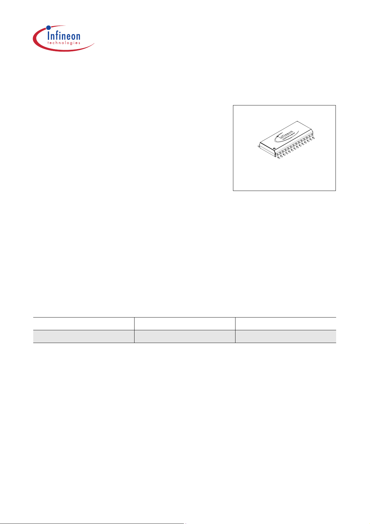
3 Pin Configuration
(top view)
Final Datasheet TLE 6263
TxD
RxD
WK2
WK1
GND GND
GND
GND GND
GND
1
2
(enhanced power package)
3
4
5
6
7
8
9
P-DSO-28-6
28
27
26
25
24
23
22
21
20
INT
RTH
CANHRO
RTL
CANL
GND
GND
DO
CLK
CSN
DI
OUTHS
10
11
12
13
14
19
18
17
16
15
V
CC
V
CI
FSO
SI
V
S
Figure 1: Pin Configuration TLE 6263 G (top view)
Version 2.08 3 2004-06-07
Page 4
Final Datasheet TLE 6263
4 Pin Definitions and Functions
Pin No. Symbol Function
1TxDTransmit data input; integrated pull up;
LOW: bus becomes dominant, HIGH: bus becomes recessive
2RxDReceive data output; push-pull output;
LOW: bus becomes dominant, HIGH: bus becomes recessive
3ROReset output; open drain output, integrated pull up, active low
4
WK2 Wake-Up input 2; for detection of external wake-up events, edge
sensitive, in sleep mode monitored by cyclic sense feature when
selected; weak pull up (2µA) to avoid unwanted wake ups
5
WK1 Wake-Up input 1; for detection of external wake-up events, edge
sensitive, in sleep mode monitored by cyclic sense feature when
selected; weak pull up (2µA) to avoid unwanted weak ups
6, 7, 8, 9,
20, 21,
GND Ground; to reduce thermal resistance place cooling areas on
PCB close to this pins.
22, 23
10 DO SPI data output; this tri-state output transfers diagnosis data to
the control device. Serial data transfered from DO is a 8 bit
diagnosis word with the Least Significant Bit (LSB) transmitted
first. The output will remain 3-stated unless the device is selected
by a LOW on Chip-Select-Not (CSN). DO will accept data on the
rising edge of CLK-signal; see table 4, 5, 6 for Diagnosis protocol
11 CLK SPI clock input; clocks the shiftregister; CLK has a pull down
input, active HIGH, and requires CMOS logic level inputs
12 CSN SPI chip select not input; CSN is a pull up input, active LOW,
serial communication is enabled by pulling the CSN terminal low;
CSN input should only be transitioned when CLK is low; CSN has
an internal active pull up and requires CMOS logic level inputs
13 DI SPI data input; receives serial data from the control device;
serial data transmitted to DI is a 8 bit control word with the Least
Significant Bit (LSB) being transferred first: the input has a pull
down input, active HIGH, and requires CMOS logic level inputs;
DI will accept data on the falling edge of CLK-signal; see table 3
for input data protocol
14 OUTHS High side switch output; controlled via SPI, in sleep mode
controlled by internal cyclic sense function when selected
Version 2.08 4 2004-06-07
Page 5
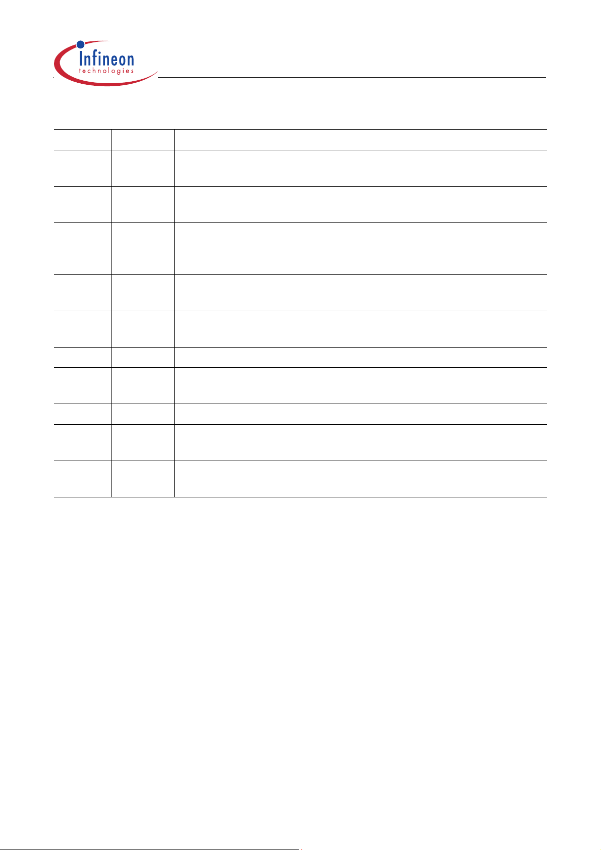
Final Datasheet TLE 6263
4 Pin Definitions and Functions (cont’d)
Pin No. Symbol Function
15 VS Power supply input; block to GND directly at the IC with ceramic
capacitor
16 SI Sense comparator input; for monitoring of external voltages, to
program the detection level connect external voltage divider
17 FSO Fail safe output; to supervise and control critical applications,
high when watchdog is correctly served, LOW at any reset
condition, open drain output, internal pull up, active LOW
18 V
19 V
CI
CC
Internal voltage supply; for stabilization of internal power
supply, block to GND with an external capacitor C
≥ 100 nF
VI
Voltage regulator output; for 5V supply, to stabilize block to
GND with an external capacitor C
≥ 100 nF
Q
24 CANL CAN-L bus line; LOW in dominant state
25 RTL CANL-Termination output; connect to CANL bus line via
termination resistor
26 CANH CAN-H bus line; HIGH in dominant state
27 RTH CANH-Termination input; connect to CANH bus line via
termination resistor
28
INT Interrupt output; to monitor wake-up events or valid sense input
condition; integrated pull up resistor; active LOW
Version 2.08 5 2004-06-07
Page 6
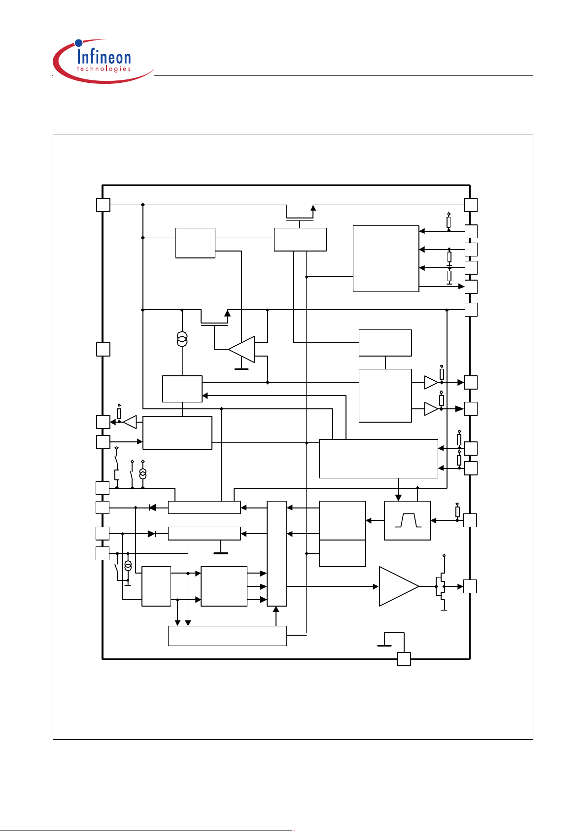
5 Functional Block Diagram
Final Datasheet TLE 6263
V
BAT
V
INT
RTL
CA NH
CA NL
RTH
CI
SI
Vcc
Vs
Vcc
Charge
Pump
Band
Gap
Early Warning
/ V
superv isor
S
H Output Stage
L Output Stage
Vcc
Driv e +
Protection
OUTHS
CSN
CLK
SPI
DI
DO
V
CC
-
+
Standby / Sleep Control
Dr iv er
Temp
Pr o t e c t
Time Bas e
Res et
Gene ra tor
+
Watchdog
CA N
Vcc
Vcc
Vcc
Vcc
Vcc
Vcc
RO
FSO
WK1
WK2
TxD
Filter
Re c ei v e r
Fail Management
Input
Stage
Rx D
CA N Fail De t ec t
GND
Figure 2: TLE 6263 G Functional Bloc Diagram
Version 2.08 6 2004-06-07
Page 7
Final Datasheet TLE 6263
6 Circuit Description
The TLE 6263 is a monolithic IC, which incorporates a failure tolerant low speed CANtransceiver for differential mode data transmission, a low dropout voltage regulator for
internal and external 5V supply as well as a SPI (serial peripheral interface) to control
and monitor the IC. Further there are integrated a high side switch, two wake-up inputs,
a window watchdog circuit with fail safe output as well as a reset circuit and early warning
function. Figure 2 shows a schematic block diagram of the TLE 6263. Table 1 shows
the status of the different chip features during the four main operation modes.
Table 1: Truth table of the TLE 6263
Feature normal mode receive-only
mode
V
CC
Reset
Watchdog
Fail safe output
-Fail
2)
V
INT
Sense input
Wake-up 1 / 2
HS-switch
4)
HS-cyclic-sense
SPI
CAN transmit
CAN receive
RTL output
ON ON ON OFF
ON ON ON OFF
ON ON
ON ON
ON ON ON ON
ON ON ON OFF
3)
ON
ON ON ON OFF
4)
OFF OFF ON ON
ON ON ON OFF
ON OFF OFF OFF
ON ON OFF OFF
switched to Vcc switched to
ON
Vcc
3)
stand-by
V
bat
mode
1)
ON
5)
ON
ON ON
switched to
Vs
sleep
mode
OFF
OFF
switched to
Vs
RxD output
INT output
1)
at low VCC output current only active when watchdog undercurrent function is not activated
2)
can only be monitored in V
3)
no wake-up interrupt generated, logic level status monitored via SPI
4)
only active when selected via SPI
5)
if watchdog under-current function active, than FSO = low
L = bus dominant;
H = bus recessive
active low early
warning
-stand-by mode via SPI
bat
L = bus dominant;
H = bus recessive
active low early
warning for V
and V
CC
INT
active low wake-up
interrupt
active low early
warning
low
low
Version 2.08 7 2004-06-07
Page 8
Final Datasheet TLE 6263
6.1 Operation Modes
The TLE 6263 offers four different operation modes that are controlled via the SPI
interface (NSTB= SPI Input Bit3, ENT=SPI Input Bit2): the normal operation mode, the
receive-only mode, the V
stand-by mode and the sleep operation mode. Please see
bat
the state diagram (figure 3).
Normal and Receive only Mode
In the normal operation mode both is possible, receiving and transmitting of messages,
in the receive-only mode (RxD-only mode) the output stages are disabled which doesn’t
allow the CAN controller to send a message to the bus. In the state diagram (figure 3),
is the status of the voltage regulator.
V
CC
SPI Input Bits:
IBit2 = ENT
IBit3 = NSTB
2)
NSTB 0
Power
Down
Normal Mo de
NSTB
ENT
11
2)
ENT 0
NSTB
2)
RxD-Only
ENT
10
2)
NSTB
2)
ENT
Sleep Mode
Sleep
ENT
NSTB
01
HS switch = OFF
1)
after 64ms1) after 500µs
V
CC
ON
ENT 1
V
CC
ON
0
1
V
CC
OFF
2)
ENT11
2)
NSTB
or
V
CC
2)
NSTB 1
Start Up
Power Up
NSTB
0
V
RT
2)
NSTB
ENT
or
V
V
NSTB
00
RxD = LOW if a wake up
occured by WK1, WK2
or CAN message
Wake Up =
transition on
WK1 or WK 2
for t > t
WU
or
CAN message
2)
ENT 1
CC
Stand-By
bat
ENT
0
0
V
RT
1)
V
ON
after 500µs
CC
1)
after 64ms
V
Stand-By Mode
bat
HS cyclic
sense
ENT
NSTB
01
HS Switch = ON
V
ON
CC
HS cyclic
sense
ENT
NSTB
01
HS Switch = ON
V
OFF
CC
1)
automatic repeated transition only if
HS cycl sense feature is s elected
by SPI IBit 4
2)
NSTB and ENT are bot h SPI Input
Bits (IBits)
Figure 3: State Diagram
V
stand-by mode and sleep mode
bat
In the V
stand-by mode and sleep mode the RTL output voltage is switched to VS.
bat
Both modes are low power modes. In the sleep mode the whole application is switched
Version 2.08 8 2004-06-07
Page 9

Final Datasheet TLE 6263
off by disabling the voltage regulator. That allows the total current consumption to drop
down to less than 100 µA.
When a reset occurs, due to false watchdog triggering, the TLE6263 automatically
switches from normal mode or receive-only mode respectively, to the V
mode. If a watchdog reset occurs in the V
stand-by mode the IC remains in this mode.
bat
stand-by
bat
In sleep mode a wake-up at any of the wake-up inputs as well as via the bus lines
(CANH or CANL) automatically sets the TLE 6263 in V
stand-by mode. In the V
bat
bat
stand-by mode a wake-up is monitored by setting the output RxD low. This feature
works as a flag, to indicate a wake event to the microcontroller. To send and to receive
messages, the CAN-transceiver has to be set to normal operation mode by the
microcontroller.
In case the IC shall directly be set back to sleep mode after a wake-up, an internal wakeflip-flop has to be reseted via the SPI. Therefore IBIT1 has to be set high and then low
again by a second SPI transmission. A transition from the V
stand-by mode to the
bat
normal mode or receive-only mode respectively, automatically resets the wake-flip-flop.
6.2 Low Dropout Voltage Regulator
The integrated low dropout voltage regulator is able to drive the internal loads (e.g.
CAN-circuit) as well as external 5V loads. Its output voltage tolerance is better than ±
2%. The maximum output current is limited to 110 mA.
An external reverse current protection is recommended at the pin Vs to prevent the
output capacitor from being discharged by negative transients or low input voltage.
Stability of the output voltage is guaranteed for output capacitors C
nevertheless it is recommended to use capacitors C
≥ 10 µF to buffer the output
Q
≥ 100 nF,
Q
voltage and therefore improve the reset behavior at input voltage transients.
To stabilize the internal supply a capacitor C
≥ 100 nF directly connected to the pin V
VI
CI
is required.
6.3 CAN Transceiver
The TLE 6263 is optimized for low speed data transmission up to 125 kBaud in
automotive applications. Figure 4 shows the principle configuration of a CAN
network.Normally a differential signal is transmitted and received respectively. When a
bus wiring failure (see table 2) is detected the device automatically switches to a
dedicated CANH or CANL single-wire mode to maintain the communication if
necessary. Further a receive-only mode is implemented that allows a separate CAN
node diagnosis. During normal and RxD-only mode, RTL is switched to V
to GND. During V
stand-by and the cyclic wake mode, RTL is switched to VS and RTH
bat
and RTH
CC
to GND.
Version 2.08 9 2004-06-07
Page 10
Final Datasheet TLE 6263
Controller 1
RxD1
Transceiver1
TxD1
BUS Line
Controller 2
RxD2
Transceiver2
TxD2
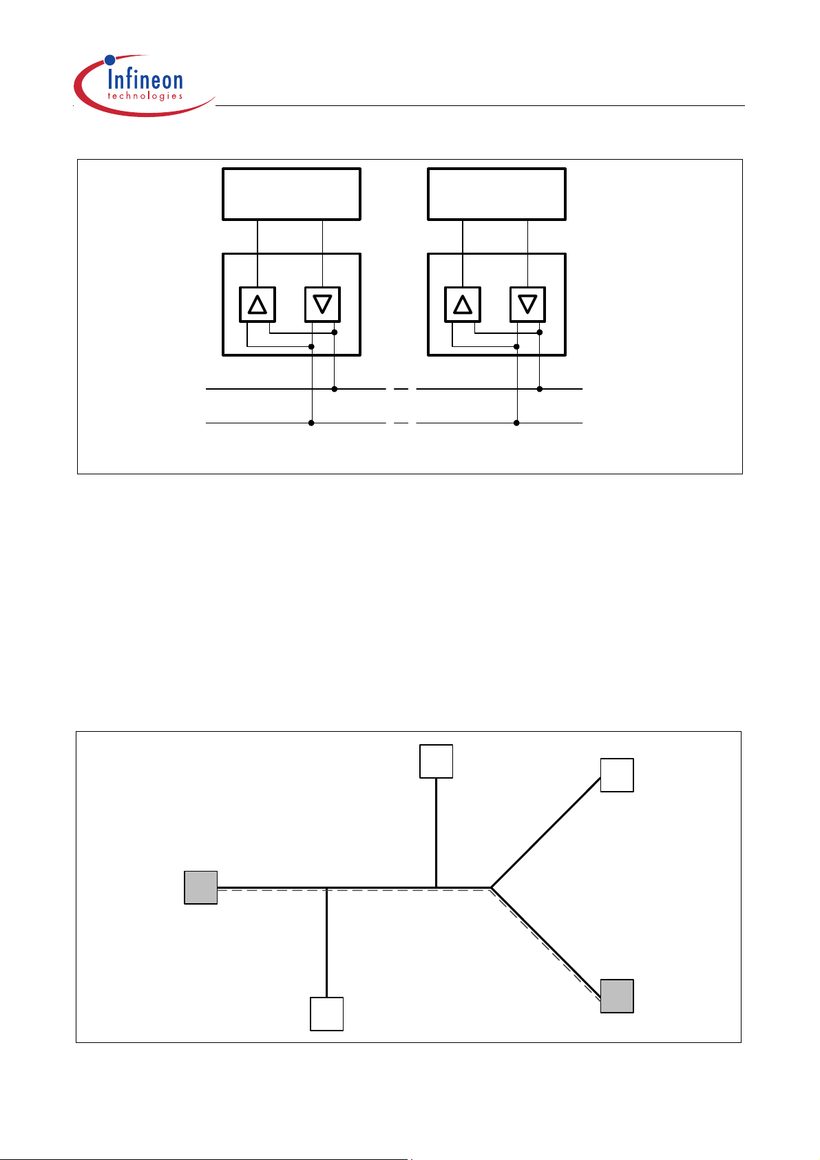
Figure 4: CAN Network Example
Receive-only Mode
The receive only mode is designed for a special test procedure to check the bus
connections. Figure 5 shows a network consisting of 5 nodes. If the connection between
node 1 and node 3 shall be tested, the nodes 2,4 and 5 are switched into receive only
mode. Node 1 and node 3 are in normal mode. If node 1 sends a message, node 3 is the
only node which can acknowledge the message, the other nodes can only listen but
cannot send an acknowledge bit. If node 1 receives the acknowledge bit from node 3,
the connection is OK.
5
1
2
4
3
Figure 5: Testing the Bus Connection in Receive-only Mode
Version 2.08 10 2004-06-07
Page 11

Final Datasheet TLE 6263
Electromagnetic Emmision (EME)
To reduce radiated electromagnetic emission (EME), the dynamic slopes of the CANL
and CANH signals are both limited and symmetric. This allows the use of an unshielded
twisted or parallel pair of wires for the bus. During single-wire transmission (one of the
bus lines is affected by a bus line failure) the EME performance of the system is
degraded from the differential mode.
6.4 Bus Failure Management
There are 9 different CAN bus wiring failures defined by the ISO 11519-2/ISO 11898-3
standard. These failures are devided into 7 failure groups (see Table 2). The difference
between ISO11898-3 and ISO 11519-2 is also shown in Table 2. When a bus wiring
failure is detected the device automatically switches to a dedicated CANH or CANL
single-wire mode to maintain the communication if necessary. Therefore it is equipped
with one differential receiver and four single ended comparators (two for each bus line).
To avoid false triggering by external RF influences, the single wire modes are activated
after a certain delay time. As soon as the bus failure disappears the transceiver switches
back to differential mode after another time delay.
The differential receiver threshold is set to typ. -2.5V. This ensures correct reception in
the normal operation mode as well as in the failure cases 1, 2, 3a(6a) and 4(5) with a
noise margin as high as possible. When one of the bus failures 3(6), 5(4), 6(3), 6a(3a),
and 7 is detected, the defective bus wire is disabled by switching off the affected bus
termination and output stage. The failure cases in brackets() are the failure cases
according to ISO 11898-3. Simultaneously the multiplexing output of the receiver circuit
is switched to the unaffected single ended comparator
The bus failures are monitored via the diagnosis protocoll of the SPI. A general indication
of a CAN failure during normal mode at CANH or CANL is reported by OBIT 4 and 5. It
is also possible to distinguish 6 CAN bus failures or failure groups on the SPI output bits
3 to 7 in the RxOnly mode(see Table 2 and 5). The failures are reported until
transmission of the next CAN word begins.
In case the transmission data input TxD is permanently dominant, both, the CANH and
CANL transmitting stage are disabled after a certain delay time t
. This is necessary
TxD
to prevent the bus from being blocked by a defective protocol unit or short to GND at the
TxD input.
In order to protect the transceiver output stages from being damaged by shorts on the
bus lines, current limiting circuits are integrated. The CANL and CANH output stage
respectively are protected by an additional temperature sensor, that disables them as
soon as the junction temperature exceeds the maximum value. In the temperature shutdown condition of the CAN output stages receiving messages from the bus lines is still
possible.
Version 2.08 11 2004-06-07
Page 12
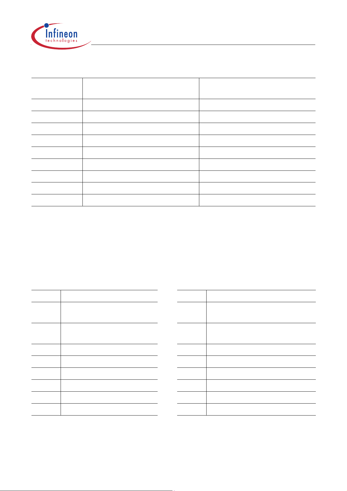
Table 2: CAN bus line failure cases
Final Datasheet TLE 6263
failure
#
failure description
according to ISO 11898-3
failure description
according to 11519-2
1 CANH line interrupted CANL line interrupted
2 CANL line interrupted CANH line interrupted
3 CANH shorted to Vbat CANL shorted to Vbat
3a CANH shorted to Vcc CANL shorted to Vcc
4 CANL shorted to GND CANH shorted to GND
5 CANH shorted to GND CANL shorted to GND
6 CANL shorted to Vbat CANH shorted to Vbat
6a CANL shorted to Vcc CANH shorted to Vcc
7 CANL shorted to CANH CANL shorted to CANH
6.5 SPI (serial peripheral interface)
The 8-bit wide programming word (input word, see table 3) is read in via the data input
DI, and this is synchronized with the clock input CLK supplied by the µC. The diagnostic
information depends on the operation mode. The internal latches for the V
-stand-by
bat
diagnosis are reseted when leaving this mode.
Table 3, Input Data Protocol Table 4, Diagnosis Data Protocol
all modes normal mode
IBIT OBIT
7 Watchdog Undercurrent
7 HS UV / Temp-Shut Down
Control
6Set V
-Fail + VCC Fail
INT
6HS Overcurrent
Flag
5 OUTHS ON 5 CANL bus fail
4 OUTHS Cyclic Sense 4 CANH bus fail
3 Not Standby 3 WK2 logic level
2 Enable Transmit 2 WK1 logic level
1 Reset Internal WK-FF 1 Window Watchdog Reset
0 Watchdog Trigger 0 Temperature Prewarning
H= ON
L= OFF
H= ON
L= OFF
Version 2.08 12 2004-06-07
Page 13

Final Datasheet TLE 6263
The transmission cycle begins when the TLE6263 is selected by the chip select not input
CSN (H to L). After the CSN input returns from L to H, the word that has been read in
becomes the new control word. The DO output switches to tri-state status at this point,
thereby releasing the DO bus circuit for other uses. For details of the SPI timing please
refer to figure 6 to 9.
Table 5, Diagnosis Data Protocol Table 6, Diagnosis Data Protocol
RxD-only mode V
-Stand-by mode
bat
OBIT OBIT
7 CAN Failure 5(4) and 7 7 V
6 CAN Failure 6 (3) 6 V
Not-Fail
CC
Not-Fail
INT
5 CAN Failure 6a (3a) 5 WK1/2 Initialization Fail
4 CAN Failure 2(1) and 4(5) 4 Wake via CAN bus lines
3 CAN Failure 3(6) 3 WK2 voltage level
2 CAN Failure 1(2) and 3a(6a) 2 WK1 voltage level
1 Window Watchdog Reset 1 Window Watchdog Reset
0 Temperature Prewarning 0 Temperature Prewarning
H= ON
L= OFF
H= ON
L= OFF
()... values in brackets according to
ISO11898-3 see table 2
6.6 Window Watchdog, Reset
When the input voltage exceeds the reset threshold voltage the reset output RO is
switched HIGH after a delay time of typ. 8ms. This is necessary for a defined start of the
microcontroller when the application is switched on. As soon as an under-voltage
condition of the output voltage (V
< VRT) appears, the reset output RO is switched
CC
LOW again (power on and under-voltage reset). The LOW signal is guaranteed down to
an output voltage V
≥ 1V. Please refer to figure 13, Reset Timing Diagram.
Q
In sleep operation mode, the watchdog circuit is automatically disabled.
Long Open Window
After the above described delayed reset (LOW to HIGH transition of RO) the window
watchdog circuit is started by opening a long open window of typ. 65ms. The long open
window allows the microcontroller to run his set-up and then to trigger the watchdog via
the SPI, refer to figure 11,Watchdog Timeout Definitions. Within the long open window
Version 2.08 13 2004-06-07
Page 14

Final Datasheet TLE 6263
period a watchdog trigger is detected as a “rising edge” by sampling a HIGH on the IBIT
0. The trigger is accepted when the CSN input becomes HIGH after the transmission of
the SPI word. After each reset as well as after a power on condition the default value of
IBIT 0 is LOW.
Closed and Open Window
A correct watchdog trigger results in starting the window watchdog by opening a closed
window of typ. 6 ms followed by a open window of typ. 10 ms. From now on the
microcontroller has to service the watchdog trigger by inverting the IBIT 0 alternating.
The “negative” or “positive” edge has to meet the open window time. A correct watchdog
service immediately results in starting the next closed window. Please refer to figure 12,
Watchdog Timing Diagram.
Watchdog Reset
Should the trigger signal not meet the open window a watchdog reset is created by
setting the reset output RO low for a period of typ. 2 ms. Then the watchdog starts again
by opening a long open window. In addition, the SPI OBIT 1 (diagnosis bit 1) is set HIGH
until the next successful watchdog trigger to monitor a watchdog reset. OBIT1 is also
HIGH until the watchdog is correctly triggered after power-up / start-up. For fail safe
reasons the TLE6263 is automatically switched in Vbat-stand-by mode if a watchdog
trigger failure occurs. So the power consumption can be minimized in case of a
permanent faulty microcontroller.
In case of either an undervoltage reset or a watchdog reset all SPI input registers (IBIT
0 to IBIT 7) are set low.
Undercurrent Disabling Function
To avoid cyclic wake-up’s of the microcontroller due to missing watchdog pulses when
the microcontroller is in a low power mode, an automatic undercurrent disabling function
of the watchdog circuit can be selected for the TLE 6263 V
activation of this feature, the V
output current in the V
CC
than the undercurrent threshold (I
CC
< I
CCWD
) and in addition the SPI IBIT 7 has to be
-stand-by mode has to be less
bat
-stand-by mode. For
bat
set HIGH. When the microcontroller returns back to normal mode or the output current
becomes higher than I
CC
> I
CCWD
the watchdog circuit is enabled again. A long open
window is started then, to ensure a simple synchronization of the watchdog timing to the
watchdog services of the microcontroller.
6.7 Flash program mode
To disable the watchdog feature a flash program mode is available. This mode is
selected by applying a voltage of 6.8V < V
< 7.2V at pin INT. This is useful e.g. if the
INT
flash-memory of the micro has to be programmed and therefore a regular watchdog
triggering is not possible. If the SPI is required in the flash program mode to change e.g.
the mode of the TLE6263 the first input telegram has to be “00000000”.
Version 2.08 14 2004-06-07
Page 15

Final Datasheet TLE 6263
6.8 Fail Safe feature
The output FSO becomes HIGH when the watchdog is correctly serviced by the
microcontroller for the fourth time
. As soon as either an under-voltage reset or watchdog
reset occurs, it is set LOW again. This feature is very useful to control critical applications
independent of the due function of the microcontroller e.g. to disable the power supply
in case of a microcontroller failure.
6.9 Sense Comparator (pin SI) and V
INT
-fail
The sense comparator (early warning function) compares a voltage defined by the user
to an internal reference voltage. Therefore the voltage to be supervised has to be scaled
down by an external voltage divider in order to compare it to the internal sense threshold
. This feature can be used e.g. to supervise the battery voltage in front of the reverse
V
SIth
protection diode. The microcontroller is given a pre-warning before an under-voltage
reset due to low input voltage occurs. The pre-warning is flagged by setting the interrupt
output INT low in normal mode, receive only mode and V
-stand-by mode. In sleep
bat
operation mode the sense function is inactive. Calculation of the voltage divider can be
easily done since the sense input current can be neglected. An internal blanking time
prevents from false triggering due to line transients. Further improvement is possible by
the use of an external ceramic capacitor switched between SI and GND (see Application
Diagram Figure 15).
6.10 V
To activate the V
internal flip-flop. This automatically sets the V
internal supply voltage become lower than the internal threshold V
NOT V
INT
- and VCC-fail flag
INT
supervisor feature the SPI IBIT 6 has to be set HIGH to set an
INT
-stand-by OBIT 6 HIGH, too. Should the
bat
VINT,th
(typ. 2.5V) the
-Fail bit becomes LOW to indicate the low voltage condition. All SPI input
registers are set LOW due to a low voltage condition of the internal supply voltage.
Like the wake-up diagnosis the V
stand-by mode. The V
-Fail feature can also be used to give an indication when the
INT
-Fail diagnosis can only be monitored in the V
INT
bat
ECU has been changed and therefore a pre-setting routine of the microcontroller has to
be started.
Further to the reset threshold there is another supervisor threshold implemented, to
monitor the output voltage V
-Fail feature is monitored via OBIT 7 in the V
V
CC
-Fail flag, via IBIT 6 (so both fail features are activated with the IBIT 6 but monitored
V
INT
via OBIT 6 and OBIT 7 during V
. This threshold is called V
CC
-stand-by mode and set, like the NOT
bat
-stand-by).
bat
VCC,th
(typ. 2.5V). The NOT
In the receive-only mode both fail bits cause the interrupt output INT to go low.
Version 2.08 15 2004-06-07
-
Page 16

Final Datasheet TLE 6263
6.11 Wake-Up Inputs WK1, WK2
In addition to a wake-up from sleep mode via the bus lines CANH or CANL it is also
possible to wake-up the TLE6263 from low power mode via the wake-up inputs WK1 and
WK2. The wake-up inputs are sensitive to a transition of the voltage level, either from
high to low or the other way round. They are active in all operation modes. In the normal
mode the current logic level at WK1/2 is monitored via the SPI (see table 4 and 6).
A positive or negative voltage edge at WK1/2 in V
-stand-by mode or sleep mode
bat
immediately results in setting the output RxD low to signal a wake-up. After a wake-up
via WK1/2 the transmission of the SPI diagnosis word in the V
-stand-by mode shows
bat
the logic level that has caused the wake-up. To get the current voltage levels at WK1/2
in the V
-stand-by mode the internal wake flip-flop has to be reseted by the IBIT1 for
bat
each transmission. As long as IBIT1 is set high or the internal wake flip-flop is reseted
respectively, in the V
-stand-by mode the RxD output is blocked to signal a new wake-
bat
up event via the CAN-bus or the wake-up inputs.
Further to the continues sensing at the wake-up inputs a cyclic sense feature is possible.
When the OUTHS cyclic sense feature is selected via the SPI IBIT 4 the high side switch
as well as the WK1/2 inputs are periodically activated by the TLE6263 in the sleep and
-stand-by mode.
V
bat
When switching the TLE6263 into sleep mode (cyclic sense feature activated) the
voltage level at the wake-inputs is sensed 2 times to initialize the reference voltage.
Should this initialisation fail (2 samples are unequal) the device is automatically set in
-stand-by mode and the initialisation error is shown on the OBIT 5. To enter the sleep
V
bat
mode now directly from the V
-stand-by mode, the internal wake flip-flop has to be
bat
reseted by the IBIT 1.
6.12 Interrupt output INT
Like the reset output, the interrupt output is a low active output. It is used to monitor low
voltage conditions at the sense input in normal mode and stand-by mode (see table 8).
In the receive-only mode the V
-fail flag and VCC supervisor are monitored.
INT
6.13 High Side Switch
The high side output OUTHS is able to switch loads up to 150 mA. Its on-resistance is
1.0 Ω typ. @ 25°C. This switch is controlled via the SPI input bits 4 and 5. In normal
mode, receive-only mode and V
-stand-by mode the high side output is switched on
bat
and off, respectively via the SPI input bit 5.
To supply external wake-up circuits in sleep mode and V
-stand-by mode the output
bat
OUTHS can be periodically switched on by the TLE6263 itself. In order to activate this
cyclic sense feature the SPI IBIT 4 has to be set high. The auto-timing period then is typ.
65 ms, the on-time is typ. 1 ms. Should there be any over-current condition at the switch
in the sleep mode (cyclic sense activated) or V
Version 2.08 16 2004-06-07
-stand-by mode a wake-up is flagged
bat
Page 17

Final Datasheet TLE 6263
via the RxD output. The over-current condition is monitored on the SPI OBIT 6 in normal
operation mode.
The SPI OBIT 0 flags a thermal pre-warning of the high side switch. By this the
microcontroller is able to reduce the power dissipation of the TLE6263 by switching off
functions of minor priority until the temperature threshold of the thermal shutdown is
reached. Further OUTHS is protected against short circuit and overload. As soon as the
under-voltage condition of the supply voltage is met (V
< V
S
UVOFF
), the switch is
automatically disabled by the under-voltage lockout circuit. Moreover the switch is
automatically disabled when a reset or watchdog reset occurs.
6.14 Hints for unused pins
SI: connect to V
S
OUTHS: leave open
WK1/2: connect to V
INT: leave open
RO: leave open
FSO: leave open
SI: switch to Vs
or leave open
S
Version 2.08 17 2004-06-07
Page 18

Final Datasheet TLE 6263
7 Electrical Characteristics
7.1 Absolute Maximum Ratings
Parameter Symbol Limit Values Unit Remarks
min. max.
Voltages
Supply voltage
Supply voltage
V
V
Regulator output voltage V
CAN bus voltage
CAN bus voltage
Logic input voltages (DI, CLK,
(CANH, CANL) V
(CANH, CANL) V
V
CSN, OSC, TxD)
Logic output voltage
V
(DO, RO, INT, RxD, FSO)
Termination input voltage
V
(RTH, RTL)
Input voltages at WK1/2 and
V
SI
Electrostatic discharge
V
voltage at pin CANH, CANL,
GND, V
Electrostatic discharge
S
V
voltage at any other pin
S
S
CC
CANH/L
CANH/L
I
DRI,RD
TL /TH
WK/SI
esd
esd
-0.3 28 V
-0.3 40 V
-0.3 5.5 V
-20 28 V
-40 40 V
-0.3 V
CC
V
+0.3
-0.3 V
CC
V
+0.3
-0.3 V
S
V
+0.3
-40 40 V
-3 3 kV
-1 1 kV
tp< 0.5s; tp/T < 0.1
VS >0 V
t
< 0.5s; tp/T < 0.1
p
0 V < VS < 24 V
0 V < V
< 5.5 V
CC
0 V < VS < 24 V
0 V < V
< 5.5 V
CC
0 V < VS < 24 V
0 V < V
< 5.5 V
CC
human body model,
C = 100 pF, R = 1.5 kΩ
human body model,
C = 100 pF, R = 1.5 kΩ
Currents
1)
Output current; Vcc
Output current; OUTHS I
Note 1): Not subject to production test - specified by design
I
CC
OUTH1
––A
1)
0.2 A
Version 2.08 18 2004-06-07
internally limited
1)
internally limited
Page 19

Final Datasheet TLE 6263
7.1 Absolute Maximum Ratings (cont’d)
Parameter Symbol Limit Values Unit Remarks
min. max.
Temperatures
Junction temperature
Storage temperature T
Note: Maximum ratings are absolute ratings; exceeding any one of these values may cause irreversible damage
to the integrated circuit.
T
j
stg
– 40 150 °C
– 50 150 °C
–
–
Version 2.08 19 2004-06-07
Page 20

Final Datasheet TLE 6263
7.2 Operating Range
Parameter Symbol Limit Values Unit Remarks
min. max.
Supply voltage
Supply voltage V
Supply voltage slew rate dV
Logic input voltage (DI, CLK,
V
S
S
/dt –0.5 5 V/µs
S
V
I
CSN, TxD)
Output capacitor
Output capacitor
SPI clock frequency
Junction temperature
C
C
f
T
CC
VI
clk
j
Thermal Resistances
Junction pin
Junction ambient
Note: Calculation of the junction temperature Tj = T
R
R
thj-pin
thj-a
V
UV OFF
V
UV OFF
20 V
40 V
– 0.3 V
CC
V
After VS rising above
V
UV ON
thermally limited
100 nF
100 460 nF
1.5 MHz
– 40 150 °C
–25K/W
–65K/W
+ P x R
amb
thj-a
Version 2.08 20 2004-06-07
Page 21

7.3 Electrical Characteristics
Final Datasheet TLE 6263
VS= 13.5 V; I
characteristics); all voltages with respect to ground; positive current defined flowing into pin; unless otherwise
specified.
= 1 mA; normal mode; all outputs open; – 40 °C<Tj<150°C (max. 125°C for CAN circuit
CC
Parameter Symbol Limit Values Unit Test Condition
min. typ. max.
Quiescent current Pin
Current consumption
IQ = IS - I
CC
Current consumption
IQ = IS - I
CC
Current consumption
IQ = IS - I
CC
Current consumption I
Current consumption I
V
S
I
Q
I
Q
I
Q
Q
Q
–5.510mA
–810mA
– 300 400 µA
–5080µA
3mA
normal mode;
I
=30mA;
CC
TxD recessive
normal mode;
I
=30mA;
CC
TxD dominant
stand-by mode;
T
=25°C; ICC=1mA;
j
Ibit 7 = H
sleep mode; Tj=25°C;
SPI Ibit 4 = L;
V
= V
CC
OUTHS active;
SPI Ibit 4 = H;
sleep mode;
V
= V
CC
CCI
CCI
= 0 V
= 0 V
Voltage Regulator; Pin V
Output voltage V
Output voltage V
Line regulation ∆V
Load regulation ∆V
CC
CC
CC
CC
CC
4.95.05.1V
4.85.05.2V
50 mV
50 mV
Power supply ripple rejection PSRR 40 dB
Output current limit I
Output current limit I
Drop voltage
VDR = VS - V
note 1) measured when the output voltage V
13.5 V input voltage V
CC
S
CCmax
CCmax
V
DR
110 120 mA
120 mA
0.5 V
has dropped 100 mV from the nominal value obtained at
CC
0.1 mA< ICC<100mA
6V<V
0A < I
6V<VS< 16 V;
I
5mA< ICC< 100mA;
V
VS< 1 Vss;
C
100Hz< f <100kHz
note 1)
V
I
note 1)
=1mA
CC
=6V
S
≥ 10µF
Q
= 0 V
CC
= 80 mA;
CC
<20V
I
< 100 µA
CC
Version 2.08 21 2004-06-07
Page 22

7.3 Electrical Characteristics (cont’d)
Final Datasheet TLE 6263
VS=13.5V; I
characteristics); all voltages with respect to ground; positive current defined flowing into pin; unless otherwise
specified.
= 1 mA; normal mode; all outputs open; – 40 °C<Tj< 150 °C (max. 125°C for CAN circuit
CC
Parameter Symbol Limit Values Unit Test Condition
min. typ. max.
Oscillator
internal oscillating frequency
Internal cycling time
-1
(1/64 * f
OSC
)
Internal cycling time
-1
(1/64 * f
OSC
)
f
OSC
t
CYL
t
CYL
0.43 0.51 0.64 ms
0.30 0.51 0.72 ms
125 kHz
sleep mode
Reset Generator; Pin RO
Reset threshold voltage
V
Reset low output voltage V
Reset high output voltage V
RT
RO
RO
4.5 4.65 4.8 V
0.2 0.4 V
4.0 VCC+
V
VCC decreasing
I
= 1mA for
RO
V
= V
or
RT
= 200 µA for
≥ 1V
I
V
CC
RO
CC
0.1
Reset pull up current
Reset reaction time t
Reset delay time (16 cyl.) t
Watchdog Generator
Watchdog trigger
Long open window (128 cyl.)
Closed window (12 cyl.)
Open window (20 cyl.)
Watchdog reset-puls time
(4 cyl.)
Watchdog undercurrent
disable threshold
I
RO
RR
RD
t
WD
t
LW
t
CW
t
OW
t
WDR
I
CCWD
20 200 500 µA
1210µs
V
RO
V
CC
6.9 8.5 12 ms
7.2 10 13.6 ms
55 65 81 ms
5.16.17.7ms
8.6 10.2 13 ms
1.723ms
0.547mA
T
j
Watchdog OFF when
I
CC
Ibit 7= H
= 0V
< V
RT
<85°C;
< I
CCWD
to RO = L
and SPI-
Version 2.08 22 2004-06-07
Page 23

7.3 Electrical Characteristics (cont’d)
Final Datasheet TLE 6263
VS= 13.5 V; I
characteristics); all voltages with respect to ground; positive current defined flowing into pin; unless otherwise
specified.
= 1 mA; normal mode; all outputs open; – 40 °C<Tj<150°C (max. 125°C for CAN circuit
CC
Parameter Symbol Limit Values Unit Test Condition
min. typ. max.
Watchdog Undercurrent
I
CCWDhys
0.5 mA
disable hysteresis
Watchdog Undercurrent
t
LHR
8µs
Tj=25°C
reaction time
Fail Safe Output; Pin FSO
Watchdog edge count
n
FS
4V
difference to set HIGH
I
Fail Safe low output voltage
V
Fail Safe high output voltage V
FS
FS
0.2 0.4 V
4.0 VCC+
0.1
V
= 1mA for
FSO
V
= V
CC
I
= 200 µA for
FSO
V
≥ 1V
CC
I
= -1mA for
FSO
V
CC ≥VRT
RT
or
Sense Input (Early Warning) SI, V
Sense In threshold voltage
Sense In threshold
V
V
SI,th
SI,hys
hysteresis
Sense Input Current
Sense reaction time t
Interrupt Out high voltage V
Interrupt Out low voltage V
Interrupt pull up current I
VCC-Fail threshold voltage V
-Fail reaction time t
V
CC
V
-Fail threshold voltage V
INT
I
SI
S,r
INThigh
INTlow
INT
VCC,th
VCC,r
VINT,th
-Fail, Interrupt Output INT
INT
2.12.32.5V
200 mV
0.1 µA
51020µs
0.7 x
V
CC
– V
CC
0–0.9V
20 150 500 µA
2.32.83.1V
5µs
1.53.24.3V
V
VSI decreasing until
INT transition to LOW
V
≥ 0V
SI
V
< V
S,th
= 0V
< V
VCC,th
to INT = low
to
-
bat
S
S
I0 = – 20 µA
I0 = 1.25 mA
V
INT
V
CC
Obit 6 = low; V
stand-by mode
proportional to V
Version 2.08 23 2004-06-07
Page 24

7.3 Electrical Characteristics (cont’d)
Final Datasheet TLE 6263
VS=13.5V; I
characteristics); all voltages with respect to ground; positive current defined flowing into pin; unless otherwise
specified.
= 1 mA; normal mode; all outputs open; – 40 °C<Tj< 150 °C (max. 125°C for CAN circuit
CC
Parameter Symbol Limit Values Unit Test Condition
min. typ. max.
Wake-Up Inputs WK1 / WK2
Wake-up threshold voltage
Minimum time for wake-up t
Input current I
V
WU
WK
WUth
234V
10 15 32 µs
-2 µA
sleep mode; Vbatstand-by mode
sleep mode; Vbatstand-by mode
VWK= 0 V
High Side Output OUTHS; (controlled by bit 4 and bit 5 of SPI input word)
Static
Drain-Source
R
DSON HS
–1.01.5Ω
–3.0Ω
T
= 25 °C
j
ON-Resistance;
I
OUTH3
= –0.15A
2.5 3.0 Ω
–5.0Ω
5.2 V ≤ VS ≤ 9V
T
= 25 °C
j
5.2 V ≤ VS ≤ 9V
Active zener voltage V
Clamp diode forward voltage V
Leakage current I
Switch ON delay time t
Switch OFF delay time t
Overcurrent shutdown
I
threshold
Shutdown delay time t
Current limit
UV-Switch-ON voltage
I
V
UV-Switch-OFF voltage V
UV-ON/OFF-Hysteresis V
Cyclic sense period
t
(128 cyl.)
OUTHS
OUTHS
QLHS
dONHS
dOFFHS
SDHS
dSDHS
OCLHS
UV ON
UV OFF
UV HY
P CS
–2 V
1V
–4 µA
20 µs
20 µs
–0.8 –0.3 –0.2 A
10 35 50 µs
–1.2 –0.6 –0.3 A
–5.26.0V
4.54.75.2V
–0.5–V
38 65 92 ms
I
I
V
CSN high to OUTHS
CSN high to OUTHS
–
VS increasing
VS decreasing
V
sleep mode
SPI-bit 4 = H,
OUTHS
OUTHS
OUTHS
UV ON
= – 0.15 A
= 0.15 A
= 0 V
– V
UV OFF
Version 2.08 24 2004-06-07
Page 25

7.3 Electrical Characteristics (cont’d)
Final Datasheet TLE 6263
VS= 13.5 V; I
characteristics); all voltages with respect to ground; positive current defined flowing into pin; unless otherwise
specified.
= 1 mA; normal mode; all outputs open; – 40 °C<Tj<150°C (max. 125°C for CAN circuit
CC
Parameter Symbol Limit Values Unit Test Condition
min. typ. max.
Cyclic sense period
(128 cyl.)
Cyclic sense ON time
t
P CS
t
CS on
55 65 80 ms
0.5 ms
Vbat-stand-by mode;
SPI-bit 4 = H;
watchdog undercurrent feature active
(1 cyl.)
CAN-Transceiver
Receiver Output R×D
HIGH level output voltage
V
OH
V
CC
V
CC
V
I0 = -250 µA
-0.9
LOW level output voltage V
OL
00.9V
I0 = 1.25 mA
Transmission Input T×D
HIGH level input voltage
threshold
LOW level input voltage
threshold
HIGH level input current
LOW level input current I
Bus Lines CANL, CANH
Differential receiver
recessive-to-dominant
threshold voltage
Differential receiver
dominant-to-recessive
threshold voltage
CANH recessive output
voltage
V
IH
V
IL
I
IH
IL
V
dRxDrd
V
dRxDdr
V
CANHr
0.3 ×
V
CC
0.52×
V
CC
0.48×
V
CC
0.7 ×
V
CC
V
V
-150 -30 -10 µA
-600 -300 -40 µA
-2.8 -2.5 -2.2 V
-3.1 -2.9 -2.5 V
0.10.20.3V
Vi = 4 V
Vi = 1 V
TxD = VCC;
R
< 4 kΩ
RTH
Version 2.08 25 2004-06-07
Page 26

7.3 Electrical Characteristics (cont’d)
Final Datasheet TLE 6263
VS=13.5V; I
characteristics); all voltages with respect to ground; positive current defined flowing into pin; unless otherwise
specified.
= 1 mA; normal mode; all outputs open; – 40 °C<Tj< 150 °C (max. 125°C for CAN circuit
CC
Parameter Symbol Limit Values Unit Test Condition
min. typ. max.
CANL recessive output
voltage
CANH dominant output
voltage
CANL dominant output
voltage
CANH output current I
CANL output current I
V
CANLr
V
CANHd
V
CANLd
CANH
CANL
V
CC
V
-0.2
V
CC
-1.4
V
CC
-1.0
V
CC
V
1.0 1.4 V
-110 -80 -50 mA
-5 5 µA
50 80 110 mA
-5 5 µA
TxD = VCC;
R
< 4 kΩ
RTL
TxD = 0 V;
I
= – 40 mA
CANH
TxD = 0 V;
I
= 40 mA
CANL
V
= 0 V;
CANH
TxD = 0 V
sleep mode;
V
= 12 V
CANH
V
= 5 V;
CANL
TxD = 0 V
sleep mode;
V
= 0 V
CANL
Voltage detection threshold
for short-circuit to battery
voltage on CANH and CANL
CANH wake-up voltage
threshold
CANL wake-up voltage
threshold
CANH single-ended receiver
threshold
CANL single-ended receiver
threshold
CANL leakage current I
CANH leakage current I
V
det(th)
V
H,wk
V
L,wk
V
CANH
V
CANL
CANLl
CANHl
6.57.38.0V
1.21.92.7V
2.23.13.9V
1.62.12.6V
2.42.93.4V
-5 5 µA
-5 5 µA
low power modes
low power modes
failure cases 3, 5, 7
recessive to dominant
failure case 6 and 6a
recessive to dominant
VCC=0V, VS=0V,
V
VCC=0V, VS=0V,
V
CANL
CANH
=13.5V
=5V
Version 2.08 26 2004-06-07
Page 27

7.3 Electrical Characteristics (cont’d)
Final Datasheet TLE 6263
VS= 13.5 V; I
characteristics); all voltages with respect to ground; positive current defined flowing into pin; unless otherwise
specified.
= 1 mA; normal mode; all outputs open; – 40 °C<Tj<150°C (max. 125°C for CAN circuit
CC
Parameter Symbol Limit Values Unit Test Condition
min. typ. max.
Termination Outputs RTL, RTH
I
RTL to V
switch-on
CC
R
RTL
40 95 Ω
=–10 mA;
o
resistance
V
RTL to BAT switch series
resistance
RTH to ground switch-on
R
R
oRTL
RTH
51530kΩ
40 95 Ω
-stand-by or
BAT
sleep mode
I
= 10 mA;
o
resistance
I
RTH output voltage V
RTH pull-down current I
RTL pull-up current I
oRTH
RTHpd
RTLpu
0.7 1.0 V
40 75 120 µA
-120 -75 -40 µA
= 1 mA; sleep mode
o
or V
failure cases 6 and 6a
failure cases 3, 3a, 5
and 7
-stand-by
BAT
RTH leakage current I
RTL leakage current I
CAN-Transceiver
Dynamic Characteristics
CANH and CANL bus output
transition time recessive-todominant
CANH and CANL bus output
transition time dominant-torecessive
Minimum dominant time for
wake-up on CANL or CANH
RTHl
RTLl
t
rd
t
dr
t
wu(min)
-5 5 µA
-5 5 µA
0.61.22.1µs
0.30.61.3µs
12 20 32 µs
VCC=0V, VS=0V,
V
=5V, Tj<85°C
RTH
VCC=0V, VS=0V
V
= 13.5 V,
RTL
T
<85°C
j
10% to 90%;
C
= 10 nF;
1
C
= 0; R
2
10% to 90%;
C
= 1 nF; C2 = 0; R1 =
1
100 Ω
Stand-by modes
= 100 Ω
1
Version 2.08 27 2004-06-07
Page 28

7.3 Electrical Characteristics (cont’d)
Final Datasheet TLE 6263
VS=13.5V; I
characteristics); all voltages with respect to ground; positive current defined flowing into pin; unless otherwise
specified.
= 1 mA; normal mode; all outputs open; – 40 °C<Tj< 150 °C (max. 125°C for CAN circuit
CC
Parameter Symbol Limit Values Unit Test Condition
min. typ. max.
Failure cases 3 and 6
t
fail
25 45 80 µs
detection time
Failure case 6a detection
2.0 4.8 8.0 ms
time
Failure cases 5 and 7
1.02.04.0ms
detection time
Failure cases 5, 6, 6a and 7
25 45 80 ms
recovery time
Failure cases 3 recovery time 250 500 750 µs
Failure cases 5 and 7
t
fail
0.41.02.4ms
Stand-by modes
detection time
Failure cases 6 and 6a
0.84.08.0ms
Stand-by modes
detection time
Failure cases 5, 6, 6a and 7
recovery time
Propagation delay
TxD-to-RxD LOW (recessive
to dominant)
t
PD(L)
0.41.02.4ms
–1.52.1µs
–1.72.4µs
–1.82.5µs
–2.02.6µs
Stand-by modes
C1 = 100 pF;
C
failures and bus failure
cases 1, 2, 3a and 4
C1 = C2 = 3.3 nF;
R
failure and failure
cases 1, 2, 3a and 4
C1 100 pF; C2 = 0;
R
cases 3, 5, 6, 6a and 7
C1 = C2 = 3.3 nF;
R
cases 3, 5, 6, 6a and 7
= 0; R
2
= 100 Ω; no bus
1
= 100 Ω; bus failure
1
=100 Ω; bus failure
1
= 100 Ω; no
1
Version 2.08 28 2004-06-07
Page 29

7.3 Electrical Characteristics (cont’d)
Final Datasheet TLE 6263
VS= 13.5 V; I
characteristics); all voltages with respect to ground; positive current defined flowing into pin; unless otherwise
specified.
= 1 mA; normal mode; all outputs open; – 40 °C<Tj<150°C (max. 125°C for CAN circuit
CC
Parameter Symbol Limit Values Unit Test Condition
min. typ. max.
Propagation delay
TxD-to-RxD HIGH (dominant
to recessive)
Edge-count difference
t
PD(H)
n
e
–1.32.0µs
–2.53.5µs
–1.32.1µs
–1.72.6µs
–4––
C1 = 100 pF;
C
= 0; R
2
failures and bus failure
cases 1, 2, 3a and 4
C1 = C2 = 3.3 nF;
R
= 100 Ω; no bus
1
failure and failure
cases 1, 2, 3a and 4
C1 100 pF; C2 = 0;
R
= 100 Ω; bus failure
1
cases 3, 5, 6, 6a and 7
C1 = C2 = 3.3 nF;
R
= 100 Ω; bus failure
1
cases 3, 5, 6, 6a and 7
=100 Ω; no
1
(falling edge) between CANH
and CANL for failure cases 1,
2, 3a and 4 detection
Edge-count difference (rising
edge) between CANH and
CANL for failure cases 1, 2,
3a and 4 recovery
TxD permanent dominant
t
disable time
SPI-Interface
Logic Inputs DI, CLK and CSN
H-input voltage threshold
V
L-input voltage threshold V
Hysteresis of input voltage V
Pull up current at pin CSN I
TxD
IH
IL
IHY
ICSN
–2––
1.32.03.5ms
– – 0.7 x
V
CC
0.3 x
V
CC
––V
V
50 200 500 mV
–100 –25 –5 µA
–
–
–
V
CSN
= 0.7 × V
CC
Version 2.08 29 2004-06-07
Page 30

7.3 Electrical Characteristics (cont’d)
Final Datasheet TLE 6263
VS=13.5V; I
characteristics); all voltages with respect to ground; positive current defined flowing into pin; unless otherwise
specified.
= 1 mA; normal mode; all outputs open; – 40 °C<Tj< 150 °C (max. 125°C for CAN circuit
CC
Parameter Symbol Limit Values Unit Test Condition
min. typ. max.
V
Pull down current at pin DI
I
ICLK/DI
525100µA
= 0.2 × V
DI
CC
and CLK
Input capacitance
at pin CSN, DI or CLK
C
I
–1015pF
Not subject to
production test specified by design
Logic Output DO
I
H-output voltage level
V
L-output voltage level V
Tri-state leakage current I
Tri-state input capacitance C
DOH
DOL
DOLK
DO
V
V
CC
– 1.0
CC
– 0.7
–V
– 0.2 0.4 V
– 10 – 10 µA
–1015pF
=1 mA
DOH
I
= – 1.6 mA
DOL
V
= V
CSN
0V < VDO < V
Not subject to
production test specified by design
CC
CC
Data Input Timing
Not subject to production test - specified by design
Clock period t
Clock high time t
Clock low time t
Clock low before CSN low t
CSN setup time t
CLK setup time t
Clock low after CSN high t
DI setup time t
DI hold time t
Input signal rise time
pCLK
CLKH
CLKL
bef
lead
lag
beh
DISU
DIHO
t
rIN
at pin DI, CLK and CSN
Input signal fall time
t
fIN
at pin DI, CLK and CSN
1000 – – ns
500 – – ns
500 – – ns
500 – – ns
500 – – ns
500 – – ns
500 – – ns
250 – – ns
250 – – ns
– –200ns
– –200ns
–
–
–
–
–
–
–
–
–
–
–
Version 2.08 30 2004-06-07
Page 31

7.3 Electrical Characteristics (cont’d)
Final Datasheet TLE 6263
VS= 13.5 V; I
characteristics); all voltages with respect to ground; positive current defined flowing into pin; unless otherwise
specified.
= 1 mA; normal mode; all outputs open; – 40 °C<Tj<150°C (max. 125°C for CAN circuit
CC
Parameter Symbol Limit Values Unit Test Condition
min. typ. max.
Data Output Timing
Not subject to production test - specified by design
DO rise time t
DO fall time t
DO enable time t
DO disable time t
DO valid time t
rDO
fDO
ENDO
DISDO
VADO
– 50 100 ns
– 50 100 ns
– – 250 ns
– – 250 ns
– 100 250 ns
CL = 100 pF
CL = 100 pF
low impedance
high impedance
VDO < 0.1 VCC;
V
> 0.9 VCC;
DO
= 100 pF
C
L
Thermal Prewarning and Shutdown (junction temperatures)
Not subject to production test - specified by design
OUTHS thermal prewarning
T
jPW
120 145 170 °C
ON temperature
OUTHS thermal prewarning
∆T –30 –K
hyst.
OUTHS thermal shutdown
T
jSD
150 175 200 °C
temp.
OUTHS thermal switch-on
T
jSO
120 – 170 °C
temp.
OUTHS thermal shutdown
∆T –30 –K
hyst.
OUTHS ratio of SD to PW
T
jSD
/ T
jPW
1.20 – –
temp.
Vcc thermal shutdown temp. T
OUTHS thermal shutdown
T
jSD
jSD
155 185 200 °C
150 °C
temp.
bit 0 of SPI
diagnosis word
–
–
–
–
–
hysteresis 15°K
(typ.)
hysteresis 15°K
(typ.)
Version 2.08 31 2004-06-07
Page 32

8 Timing Diagrams
N
C
S
h
H
g
i
S
N
C
Final Datasheet TLE 6263
t
o
o
L
w
&
s
g
i
r
n
i
e
g
d
e
f
o
C
L
:
K
D
O
s
i
e
e
l
b
a
n
a
.
d
t
S
t
s
u
n
i
f
m
r
a
o
n
i
o
i
t
s
t
n
a
r
s
f
e
r
e
d
t
o
O
t
t
u
u
p
S
-
f
i
h
t
s
i
g
R
e
t
r
e
CSN Low to High: Data from Shift-Register is
transfered to e.g. HS-Switch
CLK
DI
DO
0
actual Data
10
DI: Data will be accepted on the falling edge of CLK-Signal
previous Status
0
DO: State will change on the rising edge of CLK-Signal
eg.
OUTHS
Figure 6: SPI-Data Transfer Timing
time
7654321
765423
654321
7
01
a
w
e
D
n
1
0
+
+
actual Status
1
0
t
a
actual Dataold Data
Figure 7: SPI-Input Timing
Version 2.08 32 2004-06-07
Page 33

Final Datasheet TLE 6263
Figure 8: Turn OFF/ON Time
Figure 9: DO Valid Data Delay Time and Valid Time
Version 2.08 33 2004-06-07
Page 34

Final Datasheet TLE 6263
Figure 10: DO Enable and Disable Time
t
WD
t
CWmax
t
CWmin
closed window
min.
5.1
max.
7.2
t
OWmin
open window
10.0
save trigger area
t
OWmax
min.
13.6
max.
t / ms
18.9
Figure 11: Watchdog Time-Out Definitions
Version 2.08 34 2004-06-07
Page 35

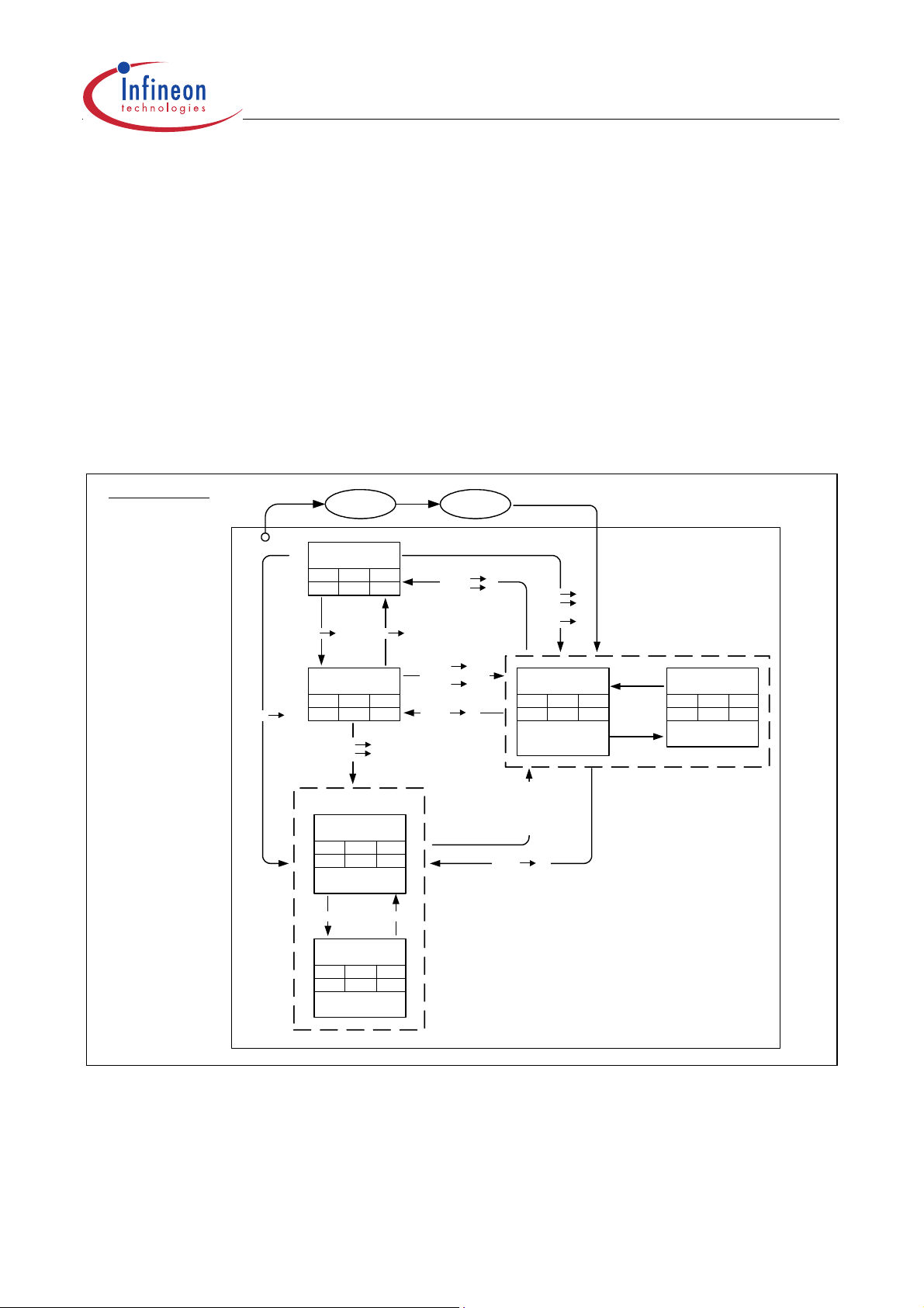
Final Datasheet TLE 6263
t
CWtOW
WD
t
CWtOW
tCW+t
OW
t
LW
Trigger
IBIT 0
t
Reset
WDR
Out
Watchdog
timer reset
normal
operation
timeout
(to long)
Figure 12: Watchdog Timing Diagram
t
LW
operation
t
CWtOW
normal
t
CW
timeout
(to short)
t
LW
t
CWtOW
t
t
normal
operation
V
CC
WD
Trigger
IBIT 0
Reset
Out
SPI
diagnosis
bit 6
-Fail
V
INT
Flag in
V
-
Stb
mode
V
RT
Watchdog
timer reset
HIGH
LOW
activation by
microcontroller
t < t
RR
V
INT-Fail
t
RD
start up start up
t
LW
t
WDR
normal operation
t
t
CWtOW
LW
t
RR
t
SR
t
RD
undervoltage
t
CW
t
LW
t
t
t
t
Figure 13: Reset Timing Diagram
Version 2.08 35 2004-06-07
Page 36

Final Datasheet TLE 6263
5 V
C
1
C
2
C
1
13.5 V
100 nF
RxD
R
1
RTH
CANH
CANL
TxD
20 pF
CSN
DO
CLK
R
1
RTL
SI
WK1
WK2
DI
INT
RO
FSO
OUTHS
V
CC
+VS
GND
V
CI
22 µF
100 nF
Figure 14: Test Circuit
Version 2.08 36 2004-06-07
Page 37

9 Application
TLE 6263
26
CANH
24
CANL
Final Datasheet TLE 6263
V
bat
CAN
bus
2
RxD
1
TxD
1 k
Ω
160 k
Ω
*)
100 k
Ω
1 k
Ω
*)
only for improvement refer to 6.9)
10 k
10nF
Ω
68 µF
27
25
16
5
100 nF
RTH
RTL
SI
OUTHS
WK2
WK1
+V
S
GND
6 - 9;
20 - 23
CSN
CLK
DO
DI
INT
RO
V
CC
FSO
V
12
11
10
13
µP
e.g. C505C,
2814
34
19
1715
18
CI
100 nF
22 µF
100 nF
C164C
GND
Figure 15: Application Circuit
Version 2.08 37 2004-06-07
Page 38

10 Package Outlines
P-DSO-28-18
(Plastic Dual Small Outline Package)
Final Datasheet TLE 6263
Sorts of Packing
Package outlines for tubes, trays etc. are contained in our
Data Book “Package Information”.
SMD = Surface Mounted Device
GPS05123
Dimensions in mm
Version 2.08 38 2004-06-07
Page 39

Final Datasheet TLE 6263
Published by
Infineon Technologies AG,
St.-Martin-Strasse 53,
D-81669 München
© Infineon Technologies AG 2001
All Rights Reserved.
Attention please!
The information herein is given to describe certain components and shall not be considered as a guarantee of
characteristics.
Terms of delivery and rights to technical change reserved.
We hereby disclaim any and all warranties, including but not limited to warranties of non-infringement, regarding
circuits, descriptions and charts stated herein.
Infineon Technologies is an approved CECC manufacturer.
Information
For further information on technology, delivery terms and conditions and prices please contact your nearest Infineon Technologies Office in Germany or our Infineon Technologies Representatives worldwide (see address list).
Warnings
Due to technical requirements components may contain dangerous substances. For information on the types in
question please contact your nearest Infineon Technologies Office.
Infineon Technologies Components may only be used in life-support devices or systems with the express written
approval of Infineon Technologies, if a failure of such components can reasonably be expected to cause the failure
of that life-support device or system, or to affect the safety or effectiveness of that device or system. Life support
devices or systems are intended to be implanted in the human body, or to support and/or maintain and sustain
and/or protect human life. If they fail, it is reasonable to assume that the health of the user or other persons may
be endangered.
Version 2.08 39 2004-06-07
Page 40

Infineon goes for Business Excellence
“Business excellence means intelligent approaches and clearly
defined processes, which are both constantly under rev iew and
ultimately lead to good operating results.
Better operating results and business excellence mean less
idleness and wastefulness for all of us, more professional
success, more accurate information, a better overview and,
thereby, less frustration and more satisfaction.”
Dr. Ulrich Schumacher
http://www.infineon.com
Published by Infineon Technologies AG
 Loading...