

现货库存、技术资料、百科信息、热点资讯,精彩尽在鼎好!
Fault Tolerant CAN - LDO TLE 6262 G
Final Data Sheet
1Overview
1.1 Features
• Standard fault tolerant differential CAN-transceiver
(TLE6254 LS CAN cell)
• Bus failure management
• Low power mode management
• CAN data transmission rate up to 125 kBaud
• Low-dropout voltage regulator 5V ± 2%
• Two Low Side Switches
• Three High Side Switches
• Power on and under-voltage reset generator
• Vcc supervisor
• Window watchdog
• Programable time base
• Integrated fail-safe mechanism
• Standard 16 bit SPI-Interface
• Wide input voltage and temperature range
• Enhanced power P-DSO-Package
P-DSO-28-6
Enhanced Power
Type Ordering Code Package
TLE 6262 G on request P-DSO-28-6
Description
The TLE 6262 G is a monolithic integrated circuit in a P-DSO-28-6 package, which
incorporates a failure tolerant low speed CAN-transceiver for differential mode data
transmission, a low dropout voltage regulator for internal and external 5V supply as well
as a 16 bit SPI interface to control and monitor the IC. Further there are integrated three
high side switches, two low side switches, a window watchdog circuit and a reset circuit.
Both, the window watchdog and reset function are referring to a time base that is
programmable via an external resistor.
The IC is designed to withstand the severe conditions of automotive applications.
1 version: 2.03 date: 2002-03-20
1.2 Pin Configuration
(top view)
Final Data TLE 6262 G
RO
1
2
3
4
5
6
7
8
9
28
27
26
25
24
23
22
21
20
OSC
PWM
TxD
RxD
Vcc
GND
GND
CANH
RTH
CANL
RTL
GND GND
GND
GND GND
GND
Figure 1
OUTH1
OUTL1
OUTL2
OUTH2
OUTH3
10
11
12
13
14
P-DSO-28-6
(enhanced power package)
19
18
17
16
15
CLK
DI
DO
CSN
Vs
2 version: 2.03 date: 2002-03-20
Final Data TLE 6262 G
1.3 Pin Definitions and Functions
Pin No. Symbol Function
1CANHCAN-H bus line; HIGH in dominant state
2RTHTermination input for CANH
3ROReset output; open drain output; integrated pull up; active low
4CANLCAN-L bus line; LOW in dominant state
5RTLTermination input for CANL
6, 7, 8, 9,
20, 21,
GND Ground; to reduce thermal resistance place cooling areas on
PCB close to this pins.
22, 23
10 OUTH1 High side output 1; controlled via PWM input and/or SPI input,
short circuit protected
11
OUTL1 Low side output 1; SPI controlled, with active zener
12 OUTL2 Low side output 2; SPI controlled, with active zener
13 OUTH2 High side output 2; SPI controlled
14 OUTH3 High side output 3; SPI controlled, in low power mode controlled
by internal autotiming function if selected
15
VS Power supply; block to GND directly at the IC with ceramic
capacitor
16 CSN SPI interface chip select not; CSN is an active low input; serial
communication is enabled by pulling the CSN terminal low; CSN
input should only be transitioned when CLK is low; CSN has an
internal active pull up and requires CMOS logic level inputs
17 DO SPI interface data out; this tristate output transfers diagnosis
data to the control device; the output will remain 3-stated unless
the device is selected by a low on Chip-Select-Not (CSN); see
table 3 for diagnosis protocol
18 DI SPI interface data in; receives serial data from the control
device; serial data transmitted to DI is a 16 bit control word with
the Least Significant Bit (LSB) being transferred first: the input
has an active pull down and requires CMOS logic level inputs; DI
will accept data on the falling edge of CLK-signal; see table 2 for
input data protocol
19 CLK SPI interface clock input; clocks the shiftregister; CLK has an
internal active pull down and requires CMOS logic level inputs
3 version: 2.03 date: 2002-03-20
1.3 Pin Definitions and Functions (cont’d)
Pin No. Symbol Function
Final Data TLE 6262 G
24 V
CC
Output voltage regulator; 5V logic supply, block to GND with an
100nF external ceramic capacitor directly at the IC + external
capacitor C
³ 22 µF
Q
25 RxD CAN Receive data output;
26 TxD CAN Transmit data input; integrated pull up
27 PWM Pulse width control; for high side switch 1
28 OSC Oscillator input; time base for power on reset, watchdog window
and stand by timer for HS3, to program connect external resistor
to GND
4 version: 2.03 date: 2002-03-20
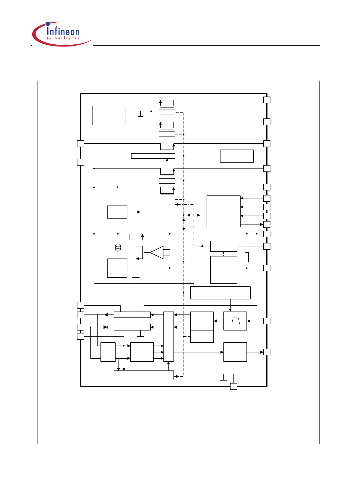
1.4 Functional Block Diagram
Final Data TLE 6262 G
OUTL1
Vs
PWM
RTL
CANH
CANL
RTH
Charge
Pump
UVLO
Band
Gap
Protection + Drive
POR
H Output Stage
L Output Stage
Drive
Drive
Drive
Drive
-
+
Switch
Fail Detect
SPI
Timer
Reset
Generator
+
Window
Watchdog
CAN
Standby / Sleep Control
Driver
Temp.
Protect
OUTL2
OUTH1
OUTH2
OUTH3
CSN
CLK
DI
DO
Vcc
OSC
RO
TxD
Figure 2
Filter
Receiver
CAN Fail Detect
Input
Fail Management
Stage
GND
RxD
5 version: 2.03 date: 2002-03-20
Final Data TLE 6262 G
1.5 Circuit Description
The TLE 6262 G is a monolithic IC, which incorporates a failure tolerant low speed CANtransceiver for differential mode data transmission, a low dropout voltage regulator for
internal and external 5V supply as well as a SPI interface to control and monitor the IC.
Further there are integrated three high side switches, two low side switches, a window
watchdog circuit and a reset circuit. Both, the window watchdog and reset function are
referring to a time base that is programmable via an external resistor.
Figure 2 shows a block schematic diagram of the TLE 6262 G
Table 1: mode truth table
Feature normal mode Receive-only
mode
V
CC
ON ON ON
V
BAT
mode
stand-by
Reset ON ON ON
Watchdog ON
1)
ON
1)
ON
1)
SPI ON ON ON
CAN transmit ON OFF OFF
CAN receive ON ON OFF
OUTHS 1
OUTHS 2
OUTHS 3
OUTHS3-auto timing
OUTLS 1
OUTLS 2
1)
at low VCC output current only active when watchdog undercurrent function is not activated
2)
a bus wake-up is monitored by setting the RxD output low
3)
only active when selected via SPI
4)
also active when driven via the PWM input
5)
automatically disabled when a reset occurs
6)
automatically disabled when a reset or watchdog reset respectively, occurs or the watchdog is disabled
by the undercurrent function
3) 4) 5)
3) 5)
3) 5)
3) 6)
3) 6)
3) 5)
ON ON ON
ON ON ON
ON ON ON
OFF ON ON
ON ON ON
ON ON ON
2)
6 version: 2.03 date: 2002-03-20

Final Data TLE 6262 G
CAN Transceiver
The TLE 6262 is optimized for low speed data transmission up to 125 kbaud in
automotive applications. Normally a differential signal is transmitted or received
respectively. When a bus wiring failure (see table 4) is detected the device automatically
switches to a dedicated CANH or CANL single-wire mode to maintain the communication
if necessary. Therefore it is equipped with one differential receiver and four single ended
comparators (two for each bus line). To avoid false triggering by external RF influences
the single wire modes are activated after a certain delay time. As soon as the bus failure
disappears the transceiver switches back to differential mode after another time delay.
The bus failures are monitored via the diagnosis protocol of the SPI. Therefore it is
possible to distinguish 6 CAN bus failures or failure groups on the bits 8 to 13 (see table
3).
To reduce EMC caused by the transceiver the dynamic slopes of the CANL and CANH
signals are both limited and symmetric. This allows the use of an unshielded twisted or
parallel pair of wires for the bus. During single-wire transmission (bus-failure) the EMC
performance of the system is degraded from the differential mode.
The differential receiver threshold is set to typ. -2.8 V. This ensures correct reception in
the normal operation mode as well as in the failure cases 1, 2, 3a and 4 with a noise
margin as high as possible. When one of the bus failures 3, 5, 6, 6a, and 7 is detected,
the defective bus wire is disabled by switching off the affected bus termination and output
stage.
The CAN-transceiver offers three different operation modes that are controlled via the
SPI: the normal operation mode, Receive-only mode and V
see the state diagram (figure 3). In the V
switched to V
.
S
stand-by mode the RTL output voltage is
bat
stand-by mode. Please
bat
In case of a wake-up via the bus lines or one of the bus lines respectively, the TLE 6262
automatically sets the RxD output LOW. To send respectively receive messages the
CAN-transceiver can now be set in normal operation mode or receive-only mode by the
microcontroller.
When a reset occurs the transceiver circuit is automatically switched to V
-stand-by
bat
mode because the SPI input bits are automatically set LOW for this event.
A thermal shutdown of the CAN-transceiver circuit is monitored via the SPI diagnosis
bit 15.
7 version: 2.03 date: 2002-03-20
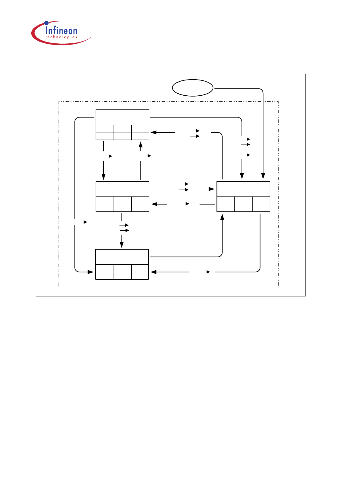
Normal Mode
Final Data TLE 6262 G
Start Up
Power Up
NSTB 0
NSTB
ENT
11
ENT 0 ENT 1
V
CC
ON
RxD-Only
NSTB
ENT
10
NSTB
ENT
V
CC
ON
0
1
Go- To-Sleep
Mode
NSTB
ENT
01
V
CC
ON
NSTB
V
CC
NSTB
NSTB
ENT
1
1
0 or
V
RT
1
ENT 1
NSTB
ENT
or
V
CC
V
Stand-By
bat
NSTB
ENT
00
0
0
V
RT
V
CC
ON
Figure 3: State Diagram
Low Dropout Voltage Regulator
The TLE 6262 is able to drive external 5V loads up to 45 mA. Its output voltage tolerance
is less than ± 2%. In addition the regulator circuit drives the internal loads like the CANtransceiver circuit.
An external reverse current protection is recommended to prevent the output capacitor
from being discharged by negative transients or low input voltage.
Stability of the output voltage is guaranteed for output capacitors C
³ 100 nF.
VCC
Nevertheless a lot of applications require a much larger output capacitance to buffer the
output voltage in case of low input voltage or negative transients. Furthermore the due
function of e.g. the reset and 3V-supervisor circuit are supported by a larger output
capacitance because of their reaction times. Therefore a output capacitance
C
³ 10 µF is recommended.
VCC
8 version: 2.03 date: 2002-03-20

Final Data TLE 6262 G
SPI (serial peripheral interface)
The 16-bit wide programming word or input word (see table 1) is read in via the data input
DI, and this is synchronized with the clock input CLK supplied by the µC. The diagnosis
word appears synchronously at the data output DO (see table 3).
The transmission cycle begins when the chip is selected by the chip select not input CSN
(H to L). After the CSN input returns from L to H, the word that has been read in becomes
the new control word. The DO output switches to tristate status at this point.
For details of the SPI timing please refer to figure 3 to 7.
Oscillator
All internal delay times are referring to the internal oscillator frequency, which is set by
an external resistor from pin OSC to GND. The oscillator frequency and the resulting
internal cycling time can be calculated by the equations:
9
´10 HzW[]
R
OSC
32
------------=
f
OSC
f
OSC
t
CYL
28 45,
-----------------------------------------=
Window Watchdog, Reset and 3V-Supervisor
When the output voltage V
exceeds the reset threshold voltage VRT the reset output
CC
RO is switched HIGH after a delay time of 16 cycles. This is necessary for a defined start
of the microcontroller when the application is switched on. As soon as an under-voltage
condition of the output voltage (V
LOW again. The LOW signal is guaranteed down to an output voltage V
< VRT) appears, the reset output RO is switched
CC
³ 1V. Please
CC
refer to fig.11, reset timing diagram.
Should the output voltage fall short of the 3V-supervisor threshold V
an internal flip-
ST
flop is set LOW. The SPI diagnosis bit 7 monitors this. In normal operation this flip-flop
has to be activated via the SPI input bit 7. This feature is useful e.g. to monitor that the
RAM data of the microcontroller might be damaged or the application is connected to V
the first time.
S
After the above described delayed reset (LOW to HIGH transition of RO) the window
watchdog circuit is started by opening a long open window of 32 cycles. Now the
microcontroller has to service a watchdog trigger signal via the SPI interface (input bit 0).
A watchdog trigger is detected as a falling edge by sampling for 2 cycles a HIGH followed
by 2 cycles LOW of the SPI input bit 0. The long open window ensures a simple and fast
9 version: 2.03 date: 2002-03-20

Final Data TLE 6262 G
synchronization of the TLE 6262 watchdog timing to the watchdog services of the
microcontroller.
After the first trigger the watchdog has to be serviced by meeting an open window of 20
cycles that follows a closed window of 12 cycles. A correct watchdog service
immediately results in starting the next closed window. Please refer to fig. 10, watchdog
timing diagram.
If the trigger signal does not meet the open window (trigger to early or to late) the reset
output RO is set LOW for a period of 4 cycles. Afterwards a long open window is started
again. In addition, the SPI diagnosis bit 2 is set HIGH to monitor a watchdog reset.
Both, the undervoltage reset and the watchdog reset are setting all SPI input bits LOW.
To avoid a cyclic wake-up of the microcontroller in low power mode (sleep mode) the
watchdog circuit can be automatically disabled at low output currents (I
CC
< I
CCWD
activate this feature the SPI input bit 8 has to be set HIGH. In this under-current mode
the low side switches are switched off automatically by the TLE 6262 to guarantee failsave operation of the application. When the microcontroller returns back to normal mode
> I
(I
CC
CCWD
) the first closed window is transformed to an open window so that the total
open window time is 32 cycles. This ensures a more simple and fast synchronization of
the TLE 6262 watchdog timing to the watchdog services of the microcontroller.
). To
Flash program mode
To disable the watchdog feature a flash program mode is available. This mode is
selected by applying a voltage of 6.8V < V
< 7.2V at pin PWM. This is useful e.g. if
PWM
the flash-memory of the micro has to be programmed and therefore a regular watchdog
triggering is not possible. If the SPI is required in the flash program mode to change e.g.
the mode of the TLE6262 the first input telegram has to be “00000000”.
High Side Switch 1
The high side output OUTH1 is able to switch loads up to 250 mA. Its on-resistance is
1.0 W typ. @ 25°C. This switch can be controlled either via the PWM input or the SPI
input bit 1. When the input PWM is used it has to be enabled by setting the SPI input bit
11 HIGH. In case of both control inputs being active the PWM signal is masked by the
SPI signal (see fig. 8, High Side Switch 1 Timing Diagram).
The SPI diagnosis bit 14 monitors a thermal shutdown of the switches, whereas bit 0
flags a thermal prewarning. By this the microcontroller is able to reduce the power
dissipation of the TLE 6262 by switching off functions of minor priority before the
temperature threshold of the thermal shutdown is reached. Further OUTH1 is protected
against short circuit and overload. The SPI diagnosis bit 1 indicates an overload of
OUTH1. As soon as the under-voltage condition of the supply voltage is met (V
V
UVOFF
), the switches are automatically disabled by the under-voltage lockout circuit.
S
<
10 version: 2.03 date: 2002-03-20

Final Data TLE 6262 G
This is flagged by the SPI diagnosis bit 3. Moreover the switches are disabled when a
reset occurs.
High Side Switch 2
The high side output OUTH2 is able to switch loads up to 250 mA. Its on-resistance is
1.0 W typ. @ 25°C. This switch is controlled via the SPI input bit 2.
The SPI diagnosis bit 14 monitors a thermal shutdown of the switches, whereas bit 0
flags a thermal prewarning. By this the microcontroller is able to reduce the power
dissipation of the TLE 6262 by switching off functions of minor priority before the
temperature threshold of the thermal shutdown is reached. As soon as the under-voltage
condition of the supply voltage is met (V
< V
S
UVOFF
disabled by the under-voltage lockout circuit. This is flagged by the SPI diagnosis bit 3.
Moreover the switches are disabled when a reset occurs.
), the switches are automatically
High Side Switch 3
The high side output OUTH3 is able to switch loads up to 150 mA. Its on-resistance is
1.5 W typ. @ 25°C. This switch is controlled via the SPI input bits 3 and 4. To supply
external wake-up circuits in low power mode (sleep mode or Vbat-stand-by mode), the
output OUTH3 can be periodically activated by the internal oscillator circuit. For
activating this feature the SPI input bits 3 and 4 have to be set HIGH. The autotiming
period is 128 internal cycle times; the on-time is 2 cycles. In case of a watchdog reset
the autotiming period may be shorter.
The SPI diagnosis bit 14 monitors a thermal shutdown of the switches, whereas bit 0
flags a thermal prewarning. By this the microcontroller is able to reduce the power
dissipation of the TLE 6262 by switching off functions of minor priority before the
temperature threshold of the thermal shutdown is reached. As soon as the under-voltage
condition of the supply voltage is met (V
< V
S
UVOFF
), the switches are automatically
disabled by the under-voltage lockout circuit. This is flagged by the SPI diagnosis bit 3.
Moreover the switches are disabled when a reset occurs.
Low Side Switches 1/2
The two low side outputs OUTL1 and OUTL2 are able to switch loads up to 100 mA.
Their on-resistance is 1.5 W (typ.) @ 25°C. This switches are controlled via the SPI input
bits 5 and 6. In case of high inrush currents a built in zener circuit (typ. 37 V) activates
the switches to protect them.
The SPI diagnosis bit 14 monitors a thermal shutdown of the switches, whereas bit 0
flags a thermal prewarning. By this the microcontroller is able to reduce the power
dissipation of the TLE 6262 by switching off functions of minor priority before the
temperature threshold of the thermal shutdown is reached. The SPI diagnosis bits 5/6
11 version: 2.03 date: 2002-03-20

Final Data TLE 6262 G
are giving a feedback about current status of OUTL1/OUTL2. As soon as the undervoltage condition of the supply voltage is met (V
< V
S
UVOFF
automatically disabled by the under-voltage lockout circuit. This is flagged by the SPI
diagnosis bit 3. In addition the outputs OUTL1 and OUTL2 are also disabled when the
watchdog is switched off in undercurrent state or when a reset occurs.
), the switches are
12 version: 2.03 date: 2002-03-20

Final Data TLE 6262 G
Table 2 Table 3
Input Data Protocol Diagnosis Data Protocol
BIT BIT
15 not used 15 Thermal Shutdown Transceiver
14 not used 14 Thermal Shutdown Switches
13 not used 13 CAN Failure 2 and 4
12 not used 12 CAN Failure 1 and 3a
11 PWM Enable 11 CAN Failure 6
10 CAN Enable Transmit 10 CAN Failure 6a
9 CAN Not Stand-By 9 CAN Failure 6a, 5 and 7
8 Watchdog Control 8 CAN Failure 3
7 Supervisor Enable 7 Vcc < 3V
6 LS-Switch 2 6 Status LS2
5 LS-Switch 1 5 Status LS1
4 HS3 Auto Timing 4 not used
3 HS-Switch 3 3 Vs Undervoltage Lockout
2 HS-Switch 2 2 Window Watchdog Reset
1 HS-Switch 1 1 Overload HS1
0 Watchdog Trigger 0 Temperature Prewarning
H= ON
L= OFF
H= ON
L= OFF
13 version: 2.03 date: 2002-03-20

Table 4
CAN bus line failure cases (according to ISO 11519-2)
Final Data TLE 6262 G
failure
failure description
#
1 CANL line interrupted
2 CANH line interrupted
3 CANL shorted to Vbat, CANL > 7.2 V
(no ISO failure) CANL shorted to Vcc; 3.2 V < CANL < 7.2 V
3a
4 CANH shorted to GND
5 CANL shorted to GND
6 CANH shorted to Vbat; CANH > 7.2 V
6a
(no ISO failure) CANH shorted to Vcc; 1.8 V < CANH < 7.2 V
7 CANL shorted to CANH
14 version: 2.03 date: 2002-03-20

Final Data TLE 6262 G
2 Electrical Characteristics
2.1 Absolute Maximum Ratings
Parameter Symbol Limit Values Unit Remarks
min. max.
Voltages
Supply voltage
V
Supply voltage V
Regulator output voltage V
CAN input voltage
CAN input voltage
(CANH, CANL) V
V
(CANH, CANL)
Logic input voltages (DI, CLK,
CSN, OSC, PWM, TxD)
Logic output voltage
(DO, RO, RxD)
Termination input voltage
(RTH, RTL)
Electrostatic discharge
voltage at pin CANH, CANL
Electrostatic discharge
voltage
V
V
V
V
V
S
S
CC
CANH/L
CANH/L
I
DO/RO/RD
TL /TH
ESD
ESD
-0.3 28 V
-0.3 40 V
-0.3 5.5 V
-10 28 V
-40 40 V
-0.3 V
CC
V
+0.3
-0.3 V
CC
V
+0.3
-0.3 V
S
V
+0.3
-4000 4000 V
-2000 2000 V
–
tp< 0.5s; tp/T < 0.1
VS >0 V
t
< 0.5s; tp/T < 0.1
p
0 V < VS < 24 V
0 V < V
0 V < VS < 24 V
0 V < V
0 V < VS < 24 V
0 V < V
human body model;
C = 100pF, R = 1.5kW
human body model;
C = 100pF, R = 1.5kW
< 5.5 V
CC
< 5.5 V
CC
< 5.5 V
CC
Currents
Output current; Vcc
Output current; OUTH1 I
Output current; OUTH2 I
Output current; OUTH3 I
Output current; OUTL1 I
Output current; OUTL2 I
I
CC
OUTH1
OUTH2
OUTH3
OUTL1
OUTL2
––A
*) 0.3 A
-0.7 0.3 A
-0.5 0.2 A
-0.2 0.4 A
-0.2 0.4 A
15 version: 2.03 date: 2002-03-20
internally limited
*) internally limited
tp< 0.5s; tp/T < 0.1
tp< 0.5s; tp/T < 0.1
tp< 0.5s; tp/T < 0.1
tp< 0.5s; tp/T < 0.1

Final Data TLE 6262 G
2.1 Absolute Maximum Ratings (cont’d)
Parameter Symbol Limit Values Unit Remarks
min. max.
Temperatures
Junction temperature
Storage temperature T
Note: Maximum ratings are absolute ratings; exceeding any one of these values may cause
irreversible damage to the integrated circuit.
T
j
stg
-40 150 °C
-50 150 °C
–
–
16 version: 2.03 date: 2002-03-20

Final Data TLE 6262 G
2.2 Operating Range
Parameter Symbol Limit Values Unit Remarks
min. max.
Supply voltage
V
Supply voltage slew rate dV
Supply voltage increasing V
Supply voltage decreasing V
Logic input voltage (DI, CLK,
V
CSN, PWM, TxD)
Output current I
Output current
CC
I
CC
Output capacitor C
SPI clock frequency
f
CLK
OSC-Adjust Resistor R
Junction temperature
T
Thermal Resistances
S
/dt -0.5 5 V/ms
S
S
S
I
V
UV OFF
-0.3 V
-0.3 V
-0.3 V
27 V
UV ON
UV OFF
CC
35 mA
45 mA
CC
22 mF
–1MHz
OSC
j
51 680 kW
-40 150 °C
V
V
V
After VS rising above
V
–
Outputs in tristate
Outputs in tristate
–
T < 0.1s
–
Ta=-40°C; f = 10kHz
–
UV ON
Junction pin
R
Junction ambient R
thj-pin
thj-a
–25K/W
–65K/W
Thermal Prewarning and Shutdown (junction temperatures)
Thermal prewarning
T
jPW
120 170 °C
ON temperature
Thermal shutdown temp. T
Ratio of SD to PW temp. T
Thermal shutdown temp. CAN T
jSD
jSD
jSD
/ T
150 200 °C
1.05 – –
jPW
135 160 °C
measured to pin 7
–
bit 0 of SPI diagnosis
word;
hysteresis 30°K (typ.)
hysteresis 30°K (typ.)
–
hysteresis 10°K (typ.)
17 version: 2.03 date: 2002-03-20

Final Data TLE 6262 G
2.3 Electrical Characteristics
9V<VS<16V; ICC= -100 mA; normal mode; all outputs open; – 40 °C<Tj< 150 °C; CAN-
T
transceiver circuitry: – 40 °C<
defined flowing into pin; unless otherwise specified.
Parameter Symbol Limit Values Unit Test Condition
< 125 °C; all voltages with respect to ground; positive current
j
min. typ. max.
Quiescent current Pin
Current consumption I
Quiescent current
I
= IS - I
SSB1
CC
Voltage Regulator; Pin V
Output voltage V
Output voltage V
Line regulation ,V
Load regulation ,V
V
S
–510mA
– 180 280 mA
4.95.05.2V
4.85.05.5V
-20 20 mV
-25 25 mV
CC
S
I
SSB1
CC
CC
CC
CC
Power supply ripple rejection PSRR 40 dB
Output current limit I
Drop voltage
VDR = VS - V
CC
CCmax
V
DR
45 60 mA
0.15 0.45 V
low power mode;
V
=12V; Tj=25°C
S
0.1mA < ICC< 30mA
0A < I
9V<VS< 15 V;
I
CC
0.1mA < ICC< 30mA;
V
S
VS< 1 Vss;
C
Q
100Hz< f <100kHz
1)
I
CC
see note 1)
CC
= 10mA
=9V
³ 22µF;
= 30 mA;
< 100µA
Oscillator; Pin OSC
Oscillating frequency
Internal cycling time
-1
(1/32 * f
1) measured when the output voltage V
voltage V
OSC
S
)
R
R
OSC
OSC
= 453kW
= 453kW
f
OSC
t
CYL
has dropped 100 mV from the nominal value obtained at 13.5 V input
CC
383 509 637 µs
62.8 kHz
18 version: 2.03 date: 2002-03-20

Final Data TLE 6262 G
2.3 Electrical Characteristics (cont’d)
9V<VS<16V; ICC=-100mA; normal mode; all outputs open; – 40 °C<Tj< 150 °C; CAN-
T
transceiver circuitry: – 40 °C<
defined flowing into pin; unless otherwise specified.
Parameter Symbol Limit Values Unit Test Condition
Reset Generator; Pin RO
<125°C; all voltages with respect to ground; positive current
j
min. typ. max.
Reset threshold voltage
Reset low output voltage
V
V
Reset high output voltage V
Reset pull up current
I
Reset reaction time t
Reset delay time (16 cyl.) t
RT
RO
RO
RO
RR
RD
4.0 4.3 4.65 V
4.0 VCC+
20 150 500 mA
1310µs
6.1 8.1 10.2 ms
3 V Supervisor; (bit 7 of SPI diagnosis word)
Supervisor threshold voltage
Supervisor reaction time
V
t
ST
SR
2.32.73.1V
2820µs
Watchdog Generator
0.2 0.4 V
V
0.1
I
= 1mA
RO
(V
³ VRT) or
CC
V
³ 1V
CC
(I
= 200 µA)
RO
V
= 0V
RO
V
< V
CC
RO = L
R
OSC
V
CC
diagnosis bit 7 = L
to
RT
= 453kW
< V
to
ST
Watchdog trigger time
Closed window time (12 cyl.) t
Open window time (20 cyl.) t
Watchdog reset-puls time
(4 cyl.)
Watchdog activating current I
Watchdog activating current
hysteresis
t
WD
CW
OW
t
WDR
CCWD
I
CCWDhys
R
7.6 10 12.3 ms
4.66.17.6ms
7.7 10.2 12.7 ms
1.52.02.6ms
2412mA
= 453kW
OSC
R
= 453kW
OSC
R
= 453kW
OSC
R
= 453kW
OSC
Tj<85°C; Watchdog
OFF when
I
< I
CC
input bit 8 = H
CCWD
and SPI-
0.5 mA
19 version: 2.03 date: 2002-03-20

Final Data TLE 6262 G
2.3 Electrical Characteristics (cont’d)
9V<VS<16V; ICC= -100 mA; normal mode; all outputs open; – 40 °C<Tj< 150 °C; CAN-
T
transceiver circuitry: – 40 °C<
defined flowing into pin; unless otherwise specified.
Parameter Symbol Limit Values Unit Test Condition
Long open window (32 cyl.) I
Switches
Under-Voltage Lockout (bit 3 of SPI diagnosis word)
< 125 °C; all voltages with respect to ground; positive current
j
min. typ. max.
R
CCWDhys
12.2 16.2 20.4 ms
= 453kW
OSC
sleep mode (WD OFF)
to normal mode
UV-Switch-ON voltage
V
UV-Switch-OFF voltage V
UV-ON/OFF-Hysteresis V
UV ON
UV OFF
UV HY
– 5.35 6.00 V
4.50 4.85 5.20 V
–0.5–V
VS increasing
VS decreasing
V
UV ON
– V
High Side Output OUTH1; (controlled by PWM or bit 1 of SPI input word)
Static Drain-Source
R
ON-Resistance;
I
OUTH1
= -0.25 A
Active zener voltage V
Clamp diode forward voltage V
Leakage current I
Switch ON delay time t
Switch OFF delay time t
Overcurrent shutdown
I
DSON H1
OUTH1
OUTH1
OLH1
dONH1
dOFFH1
SDH1
–1.02.0W
1.5 4.0 W
-5.0 -3.0 -0.5 V
0.8 1 V
-100 -5 – µA
10 100 ms
20 100 ms
-1.0 -0.6 -0.3 A
5.2 V £ VS £ 9V
I
I
V
PWM to OUTH1;
R
PWM to OUTH1;
R
–
OUTH1
OUTH1
OUTH1
= 100 W
L
= 100 W
L
= – 0.25 A
= 0.25 A
= 0 V
threshold
UV OFF
Shutdown delay time t
Current limit
dSDH1
I
OCLH1
10 25 50 ms
-2.0 -1.0 -0.5 A
20 version: 2.03 date: 2002-03-20

Final Data TLE 6262 G
2.3 Electrical Characteristics (cont’d)
9V<VS<16V; ICC=-100mA; normal mode; all outputs open; – 40 °C<Tj< 150 °C; CAN-
T
transceiver circuitry: – 40 °C<
defined flowing into pin; unless otherwise specified.
Parameter Symbol Limit Values Unit Test Condition
PWM Input to control OUTH1; Pin PWM (high active)
<125°C; all voltages with respect to ground; positive current
j
min. typ. max.
H-input voltage threshold
V
L-input voltage threshold V
Hysteresis of input voltage V
Pull down current I
Input capacitance C
IH
IL
IHY
I
I
––0.7
V
´
0.2
´V
––V
cc
V
CC
50 200 500 mV
5 25 180 mA
–1015pF
High Side Output OUTH2; (controlled by bit 2 of SPI input word)
Static Drain-Source
R
ON-Resistance;
I
OUTH2
= -0.25 A
Active zener voltage V
Clamp diode forward voltage V
Leakage current I
Switch ON delay time t
Switch OFF delay time t
DSON H2
OUTH2
OUTH2
OLH1
dONH1
dOFFH1
–1.02.0W
1.5 4.0 W
-5.0 -3.0 -0.5 V
0.8 1 V
-100 -5 – µA
10 100 µs
20 100 µs
–
–
–
VI = 0.2 * V
0V < V
5.2 V £ VS £ 9V
I
OUTH2
I
OUTH2
V
OUTH2
CSN high to OUTH2;
R
= 100 W
L
CSN high to OUTH2;
R
= 100 W
L
CC
< 5.25 V
CC
= – 0.25 A
= 0.25 A
= 0 V
High Side Output OUTH3; (controlled by bit 3 and bit 4 of SPI input word)
Static Drain-Source
R
ON-Resistance;
I
OUTH3
= -0.15 A
Active zener voltage V
Clamp diode forward voltage V
Leakage current I
DSON H3
OUTH3
OUTH3
OLH3
–1.53.0W
2.0 5.0 W
-5.0 -3.0 -0.5 V
0.8 1 V
-100 -5 – µA
21 version: 2.03 date: 2002-03-20
5.2 V £ VS £ 9V
I
= – 0.15 A
OUTH3
I
= 0.15 A
OUTH3
V
OUTH3
= 0 V

Final Data TLE 6262 G
2.3 Electrical Characteristics (cont’d)
9V<VS<16V; ICC= -100 mA; normal mode; all outputs open; – 40 °C<Tj< 150 °C; CAN-
T
transceiver circuitry: – 40 °C<
defined flowing into pin; unless otherwise specified.
Parameter Symbol Limit Values Unit Test Condition
< 125 °C; all voltages with respect to ground; positive current
j
min. typ. max.
Leakage current I
Switch ON delay time t
Switch OFF delay time t
Auto time period
OLH3
dONH3
dOFFH3
t
PH3
–5 µA
10 100 µs
20 100 µs
49 65 82 ms
(128 cyl.)
Auto time ON duty cycle
D.C. 1/64
(2 cyl.)
Low Side Output OUTL1 (bit 5 of SPI input word)
Static Drain-Source
R
ON-Resistance;
I
OUTL1
= 0.1 A
Active zener clamp voltage V
Leakage current I
Switch ON delay time t
Switch OFF delay time t
DSON L1
OUTL1
OLL1
dONL1
dOFFL1
–1.53.0W
2.0 5.0 W
32 37 42 V
550µs
550µs
V
CSN high to OUTH3;
R
CSN high to OUTH3;
R
R
SPI-bit 4 = H,
no WD reset
referring to t
5.2 V £ VS £ 9V
I
OUTL1
5µA
V
T
CSN high to OUTL1;
R
CSN high to OUTL1;
R
OUTH3
= 100 W
L
= 100 W
L
= 453kW;
OSC
= – 0.1 A
OUTL1
< 85°C
j
= 100 W
L
= 100 W
L
= 5 V
PH3
=15 V;
Low Side Output OUTL2 (bit 6 of SPI input word)
Static Drain-Source
R
ON-Resistance;
I
OUTL2
= 0.1 A
Active zener clamp voltage V
Leakage current I
Switch ON delay time t
Switch OFF delay time t
DSON L2
OUTL2
OLL2
dONL2
dOFFL2
–1.53.0W
2.0 5.0 W
32 37 42 V
550µs
550µs
22 version: 2.03 date: 2002-03-20
5.2 V £ VS £ 9V
I
OUTL2
5µA
V
T
CSN high to OUTL2;
R
CSN high to OUTL2;
R
= – 0.1 A
OUTL2
< 85°C
j
= 100 W
L
= 100 W
L
=15 V;

Final Data TLE 6262 G
2.3 Electrical Characteristics (cont’d)
9V<VS<16V; ICC=-100mA; normal mode; all outputs open; – 40 °C<Tj< 150 °C; CAN-
T
transceiver circuitry: – 40 °C<
defined flowing into pin; unless otherwise specified.
Parameter Symbol Limit Values Unit Test Condition
CAN-Transceiver
<125°C; all voltages with respect to ground; positive current
j
min. typ. max.
Receiver Output R
HIGH level output voltage
´D
V
LOW level output voltage V
Transmission Input T´D
HIGH level input voltage
V
threshold
LOW level input voltage
V
threshold
HIGH level input current I
LOW level input current I
Bus Lines CANL, CANH
Differential receiver
V
recessive-to-dominant
threshold voltage
OH
OL
IH
IL
IH
IL
dRxD(rd)
V
CC
–
V
CC
V
– 0.9
0–0.9V
0.30´
V
CC
0.52´
V
CC
0.48´
V
CC
0.70´
V
CC
V
V
-140 -40 -10 µA
-600 -200 -40 µA
-2.8 -2.5 -2.2 V
I0 = – 250µA
I0 = 1.25mA
Vi = 4 V
Vi = 1 V
Differential receiver
dominant-to-recessive
threshold voltage
CANH recessive output
voltage
CANL recessive output
voltage
CANH dominant output
voltage
V
dRxD(dr)
V
CANHr
V
CANLr
V
CANHd
-3.1 -2.9 -2.5 V
0.1 0.2 0.3 V
V
CC
––
V
- 0.2
V
CC
-1.4
23 version: 2.03 date: 2002-03-20
V
CC
-1.0
V
CC
V
TxD = VCC;
R
< 4 kW
RTH
TxD = VCC;
R
< 4 kW
RTL
TxD = 0 V;
I
= – 40 mA
CANH

Final Data TLE 6262 G
2.3 Electrical Characteristics (cont’d)
9V<VS<16V; ICC= -100 mA; normal mode; all outputs open; – 40 °C<Tj< 150 °C; CAN-
T
transceiver circuitry: – 40 °C<
defined flowing into pin; unless otherwise specified.
Parameter Symbol Limit Values Unit Test Condition
< 125 °C; all voltages with respect to ground; positive current
j
min. typ. max.
CANL dominant output
voltage
CANH output current I
CANL output current I
Voltage detection threshold
for short-circuit to battery
voltage on CANH and CANL
CANH wake-up voltage
threshold
CANL wake-up voltage
threshold
CANH single-ended receiver
threshold
V
CANLd
CANH
CANL
V
det(th)
V
WAKEH
V
WAKEL
V
CANH
–1.01.4V
-110 -80 -50 mA
-5 0 5 µA
50 80 110 mA
-5 0 5 µA
6.5 7.3 8.0 V
1.2 1.9 2.7 V
2.2 3.1 3.9 V
1.6 2.1 2.6 V
TxD = 0 V;
I
= 40 mA
CANL
V
= 0 V;
CANH
TxD = 0 V
sleep mode;
V
= 12 V
CANH
V
= 5 V;
CANL
TxD = 0 V
sleep mode;
V
= 0 V;
CANL
V
= 0 V
S
normal operation
mode
–
–
failure cases 3, 5 and
7
CANL single-ended receiver
V
threshold
CANL leakage current I
CANH leakage current I
CANLl
CANHl
Termination Outputs RTL, RTH
RTL to V
switch-on
CC
R
resistance
RTL to BAT switch series
R
resistance
CANL
RTL
oRTL
2.4 3.0 3.4 V
-5 0 5 µA
-5 0 5 µA
–4095W
51530kW
failure case 6 and 6a
VCC=0V, VS=0V,
V
T
VCC=0V;VS=0V;
V
T
Io =–10 mA;
V
CANL
<85°C
j
CANH
<85°C
j
-stand-by
BAT
=13.5V,
=5V;
24 version: 2.03 date: 2002-03-20

Final Data TLE 6262 G
2.3 Electrical Characteristics (cont’d)
9V<VS<16V; ICC=-100mA; normal mode; all outputs open; – 40 °C<Tj< 150 °C; CAN-
T
transceiver circuitry: – 40 °C<
defined flowing into pin; unless otherwise specified.
Parameter Symbol Limit Values Unit Test Condition
<125°C; all voltages with respect to ground; positive current
j
min. typ. max.
RTH to ground switch-on
R
resistance
RTH output voltage V
RTH pull-down current I
RTL pull-up current I
RTH
oRTH
RTHpd
RTLpu
– 40 95 W
– 0.7 1.0 V
40 75 120 µA
-120 -75 -40 µA
Io = 10 mA
Io = 1 mA;
Vbat-stand-by mode
failure cases 6 and 6a
failure cases 3, 3a, 5
and 7
25 version: 2.03 date: 2002-03-20

Final Data TLE 6262 G
2.3 Electrical Characteristics (cont’d)
9V<VS<16V; ICC= -100 mA; normal mode; all outputs open; – 40 °C<Tj< 150 °C; CAN-
T
transceiver circuitry: – 40 °C<
defined flowing into pin; unless otherwise specified.
Parameter Symbol Limit Values Unit Test Condition
CAN-Transceiver
Dynamic Characteristics
< 125 °C; all voltages with respect to ground; positive current
j
min. typ. max.
CANH and CANL bus output
t
rd
0.6 1.2 2.1 µs
transition time recessive-todominant
CANH and CANL bus output
t
dr
0.3 0.6 1.3 µs
transition time dominant-torecessive
Minimum dominant time for
t
wu(min)
12 20 38 µs
wake-up on CANL or CANH
Failure cases 3 and 6
t
fail
30 45 80 µs
detection time
Failure case 6a detection
2.04.88.0ms
time
Failure cases 5, 6, 6a and 7
30 45 80
µs
recovery time
Failure cases 3 recovery time 250 500 750 µs
Failure cases 5 and 7
1.02.04.0ms
detection time
10% to 90%;
C
= 10 nF;
1
C
= 0; R1 = 100 W
2
10% to 90%;
C
= 1 nF; C2 = 0; R1 =
1
100 W
stand-by mode;
V
= 13.5 V
S
Failure cases 5 detection
time
Failure cases 6, 6a and 7
detection time
Failure cases 5, 6, 6a and 7
recovery time
t
fail
0.41.02.4ms
0.84.08.0ms
0.4 1.0 2.4 µs
stand-by modes;
V
= 13.5 V
S
stand-by modes;
V
= 13.5 V
S
stand-by modes;
V
= 13.5 V
S
26 version: 2.03 date: 2002-03-20

Final Data TLE 6262 G
2.3 Electrical Characteristics (cont’d)
9V<VS<16V; ICC=-100mA; normal mode; all outputs open; – 40 °C<Tj< 150 °C; CAN-
T
transceiver circuitry: – 40 °C<
defined flowing into pin; unless otherwise specified.
Parameter Symbol Limit Values Unit Test Condition
<125°C; all voltages with respect to ground; positive current
j
min. typ. max.
Propagation delay
TxD-to-RxD LOW (recessive
to dominant)
Propagation delay
TxD-to-RxD HIGH (dominant
to recessive)
t
PD(L)
t
PD(H)
– 1.5 2.1 µs
– 1.7 2.4 µs
– 1.8 2.5 µs
– 2.0 2.6 µs
– 1.5 2.0 µs
– 2.5 3.5 µs
– 1.0 2.1 µs
C1 = 100 pF;
C
= 0; R1 = 100 W; no
2
failures and bus failure
cases 1, 2, 3a and 4
C1 = C2 = 3.3 nF;
R
= 100 W; no bus
1
failure and failure
cases 1, 2, 3a and 4
C1 100 pF; C2 = 0;
R
= 100 W; bus failure
1
cases 3, 5, 6, 6a and 7
C1 = C2 = 3.3 nF;
R
=100 W; bus failure
1
cases 3, 5, 6, 6a and 7
C1 = 100 pF;
C
= 0; R1 =100 W; no
2
failures and bus failure
cases 1, 2, 3a and 4
C1 = C2 = 3.3 nF;
R
= 100 W; no bus
1
failure and failure
cases 1, 2, 3a and 4
C1 100 pF; C2 = 0;
R
= 100 W; bus failure
1
cases 3, 5, 6, 6a and 7
Edge-count difference
(falling edge) between CANH
and CANL for failure cases 1,
2, 3a and 4 detection
Edge-count difference (rising
edge) between CANH and
CANL for failure cases 1, 2,
3a and 4 recovery
TxD permanent dominant
disable time
n
t
e
TxD
– 1.5 2.6 µs
C1 = C2 = 3.3 nF;
R
= 100 W; bus failure
1
cases 3, 5, 6, 6a and 7
– 4 ––
– 2 ––
1.32.03.5ms
27 version: 2.03 date: 2002-03-20

Final Data TLE 6262 G
2.3 Electrical Characteristics (cont’d)
9V<VS<16V; ICC= -100 mA; normal mode; all outputs open; – 40 °C<Tj< 150 °C; CAN-
T
transceiver circuitry: – 40 °C<
defined flowing into pin; unless otherwise specified.
Parameter Symbol Limit Values Unit Test Condition
SPI-Interface
Logic Inputs DI, CLK and CSN
< 125 °C; all voltages with respect to ground; positive current
j
min. typ. max.
H-input voltage threshold
V
L-input voltage threshold V
Hysteresis of input voltage V
Pull up current at pin CSN I
Pull down current at pin DI
I
and CLK
Input capacitance
C
at pin CSN, DI or CLK
Logic Output DO
H-output voltage level
V
L-output voltage level V
Tri-state leakage current I
Tri-state input capacitance C
IH
IL
IHY
ICSN
ICLK/DI
I
DOH
DOL
DOLK
DO
––0.7 *
V
CC
0.3 *
V
CC
––V
V
50 200 500 mV
-100 -25 -5 mA
525100mA
–1015pF
V
V
CC
– 1.0
CC
– 0.7
–V
– 0.2 0.4 V
-10 – 10 mA
–1015pF
–
–
–
V
VDI = 0.2 ´ V
0V < VCC < 5.25 V
I
DOH
I
DOL
V
0V < VDO < V
V
0 V < VCC < 5.25 V
= 0.7 ´ V
CSN
=1 mA
= – 1.6 mA
= V
CSN
= V
CSN
CC
CC
CC
CC
CC
Data Input Timing
Clock period
Clock high time t
Clock low time t
Clock low before CSN low t
t
pCLK
CLKH
CLKL
bef
1000 – – ns
500 – – ns
500 – – ns
500 – – ns
–
–
–
–
28 version: 2.03 date: 2002-03-20

Final Data TLE 6262 G
2.3 Electrical Characteristics (cont’d)
9V<VS<16V; ICC=-100mA; normal mode; all outputs open; – 40 °C<Tj< 150 °C; CAN-
T
transceiver circuitry: – 40 °C<
defined flowing into pin; unless otherwise specified.
Parameter Symbol Limit Values Unit Test Condition
<125°C; all voltages with respect to ground; positive current
j
min. typ. max.
CSN setup time t
CLK setup time t
Clock low after CSN high t
DI setup time t
DI hold time t
Input signal rise time
at pin DI, CLK and CSN
Input signal fall time
at pin DI, CLK and CSN
Data Output Timing
DO rise time
DO fall time t
DO enable time t
DO disable time t
DO valid time t
lead
lag
beh
DISU
DIHO
t
rIN
t
fIN
t
rDO
fDO
ENDO
DISDO
VADO
500 – – ns
500 – – ns
500 – – ns
250 – – ns
250 – – ns
– – 200 ns
– – 200 ns
– 50 100 ns
– 50 100 ns
– – 250 ns
– – 250 ns
– 100 250 ns
–
–
–
–
–
–
–
CL = 100 pF
CL = 100 pF
low impedance
high impedance
VDO < 0.2 VCC;
V
> 0.7VCC;
DO
C
= 100 pF
L
29 version: 2.03 date: 2002-03-20

3 Timing Diagrams
CSN High to Low & rising edge of CLK: DO is enabled. Status information is transfered to Output Shift Register
CSN
CSN Low to High: Data from Shift-Register is transfered to Output Power Switches
Final Data TLE 6262 G
time
CLK
DI
DO
eg.
HS1
12345678910
0
0 141312
1
__
0 141312
1
Figure 4
Data Transfer Timing
14
15
15
15
______________
11 12
actual Data
__
432
5
DI: Data will be accepted on the falling edge of CLK-Signal
432
5
DO: State will change on the rising edge of CLK-Signal
76
8
previous Status
76
8
109
109
13
11
11
10
new Data
01
++
actual Status
0
1
actual Dataold Data
30 version: 2.03 date: 2002-03-20

Final Data TLE 6262 G
Figure 5
SPI-Input Timing
Figure 6
Turn OFF/ON Time
31 version: 2.03 date: 2002-03-20

Final Data TLE 6262 G
Figure 7
DO Valid Data Delay Time and Valid Time
Figure 8
DO Enable and Disable Time
32 version: 2.03 date: 2002-03-20

Figure 9: High Side Switch1 Timing Diagram
SPI input
bit 1
H
L
Final Data TLE 6262 G
PWM
(SPI input
bit 11 = H)
HS-
Switch1
t
H
L
t
ON
OFF
t
33 version: 2.03 date: 2002-03-20

Figure 10: Watchdog Time-out Definitions
t
WD
Final Data TLE 6262 G
t
CW
closed window open window
Figure 11: Watchdog Timing Diagram
t
CWtOW
WD
Trigger
t
LOW
tCW+t
OW
t
LOW
t
t
LOW
OW
t
CWtOW
t / ms
t
LOW
t
CW
t
CWtOW
Reset
Out
Watchdog
timer reset
normal
operation
t
WDR
timeout
(to long)
t
t
normal
operation
timeout
(to short)
normal
operation
34 version: 2.03 date: 2002-03-20

Figure 12: Reset Timing Diagram
Final Data TLE 6262 G
Vcc
WD
Trigger
Reset
Out
SPI
diagnosis
bit 7
V
RT
V
ST
t
Watchdog
timer reset
RD
t
LOW
t
WDR
start up start up
HIGH
LOW
activation by
microcontroller
t < t
RR
t
t
LOW
CWtOW
normal operation
t
t
CW
t
RR
RD
undervoltage
t
SR
t
LOW
t
t
CW
t
t
t
35 version: 2.03 date: 2002-03-20

4 Application
Final Data TLE 6262 G
V
bat
CAN bus
22 µF
68 nF
+V
S
CANH
CANL
RTH
RTL
OUTL2
OUTL1
OUTH3
OUTH2
OUTH1
CSN
CLK
DI
DQ
TxD
RxD
PWM
RQ
Vcc
OSC
GND
453 k
µP
22 µF
9
GND
Figure 13
Application Circuit
TLE 6262 G
36 version: 2.03 date: 2002-03-20

5 Package Outlines
P-DSO-28-6
(Plastic Dual Small Outline Package)
Final Data TLE 6262 G
Sorts of Packing
Package outlines for tubes, trays etc. are contained in our
Data Book “Package Information”.
GPS05123
Dimensions in mm
37 version: 2.03 date: 2002-03-20

Final Data TLE 6262 G
Edition 1999-10-12
Published by Infineon Technologies AG
St.-Martin-Strasse 53
D-81541 München
© Infineon Technologies AG1999
All Rights Reserved.
Attention please!
The information herein is given to describe certain components and shall not be considered as warranted characteristics.
Terms of delivery and rights to technical change reserved.
We hereby disclaim any and all warranties, including but not limited to warranties of non-infringement, regarding circuits, descriptions and
charts stated herein.
Infineon Technologies is an approved CECC manufacturer.
Information
For further information on technology, delivery terms and conditions and prices please contact your nearest Infineon Technologies Office
in Germany or our Infineon Technologies Representatives worldwide (see address list).
Warnings
Due to technical requirements components may contain dangerous substances. For information on the types in question please contact
your nearest Infineon Technologies Office.
Infineon Technologies Components may only be used in life-support devices or systems with the express written approval of Infineon Technologies, if a failure of such components can reasonably be expected to cause the failure of that life-suppor t device or system, or to affect
the safety or effectiveness of that device or system. Life support devices or systems are intended to be implanted in the human body, or to
support and/or maintain and sustain and/or protect human life. If they fail, it is reasonable to assume that the health of the user or other
persons may be endangered.
38 version: 2.03 date: 2002-03-20
 Loading...