


Final Datasheet, Version 2.06, 2003-02-21
现货库存、技术资料、百科信息、热点资讯,精彩尽在鼎好!
LIN Transceiver
TLE 6259-2
Automotive and
Industrial
Never stop thinking.

Single-Wire-Transceiver TLE 6259-2
Final Datasheet
1Overview
1.1 Features
• Single-wire transceiver, suitable for LIN protocol
• Transmission rate up to 20 kBaud
• Compatible to LIN specification 1.2
• Compatible to ISO 9141 functions
• Very low current consumption in sleep mode
• Control output for voltage regulator
• Bus short to GND protection
• Short circuit proof to ground and battery
• Overtemperature protection
P-DSO-8-3, -6
Type Ordering Code Package
TLE 6259-2G Q 67006 - A 9596 P-DSO-8-3
Description
The TLE 6259-2 is a monolithic integrated circuit in a P-DSO-8-3 package. It works as
an interface between the protocol controller and the physical bus. The TLE 6259-2 is
especially suitable to drive the bus line in LIN systems in automotive and industrial
applications. Further it can be used in standard ISO9141 systems. The TLE6259-2 has
a BUS short to GND feature implemented, to avoid a battery decharge.
In order to reduce the current consumption, the TLE 6259-2 offers a sleep operation
mode. In this mode a voltage regulator can be controlled to minimize the current
consumption of the whole application. A wake-up caused by a message on the bus,
enables the voltage regulator and sets the RxD output LOW until the device is switched
to normal operation mode.
®
The IC is based on the Smart Power Technology SPT
which allows bipolar and CMOS
control circuitry in accordance with DMOS power devices existing on the same
monolithic circuit.
The TLE 6259-2 is designed to withstand the severe conditions of automotive
applications.
Version 2.06 2 2003-02-21
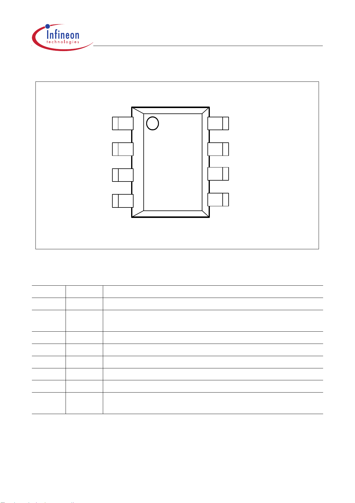
1.2 Pin Configuration (top view)
Final Datasheet TLE 6259-2
RxD
EN
TxD
Figure 1
1.3
Pin Definitions and Functions:
Pin No. Symbol Function
1
2
3
4
P-DSO-8-3
8
7
6
5
INH
Vs
BusVcc
GND
1RxDReceive data output; integrated pull up, LOW in dominant state,
2ENEnable input; integrated 30 kW pull down, transceiver in normal
operation mode when HIGH
3V
CC
5V supply input;
4TxDTransmit data input; integrated pull up, LOW in dominant state
5GNDGround;
6BusBus output/input; internal 30 kW pull up, LOW in dominant state
7VsBattery supply input;
8INHInhibit output; to control a voltage regulator, becomes HIGH
when wake-up via LIN bus occurs
Version 2.06 3 2003-02-21
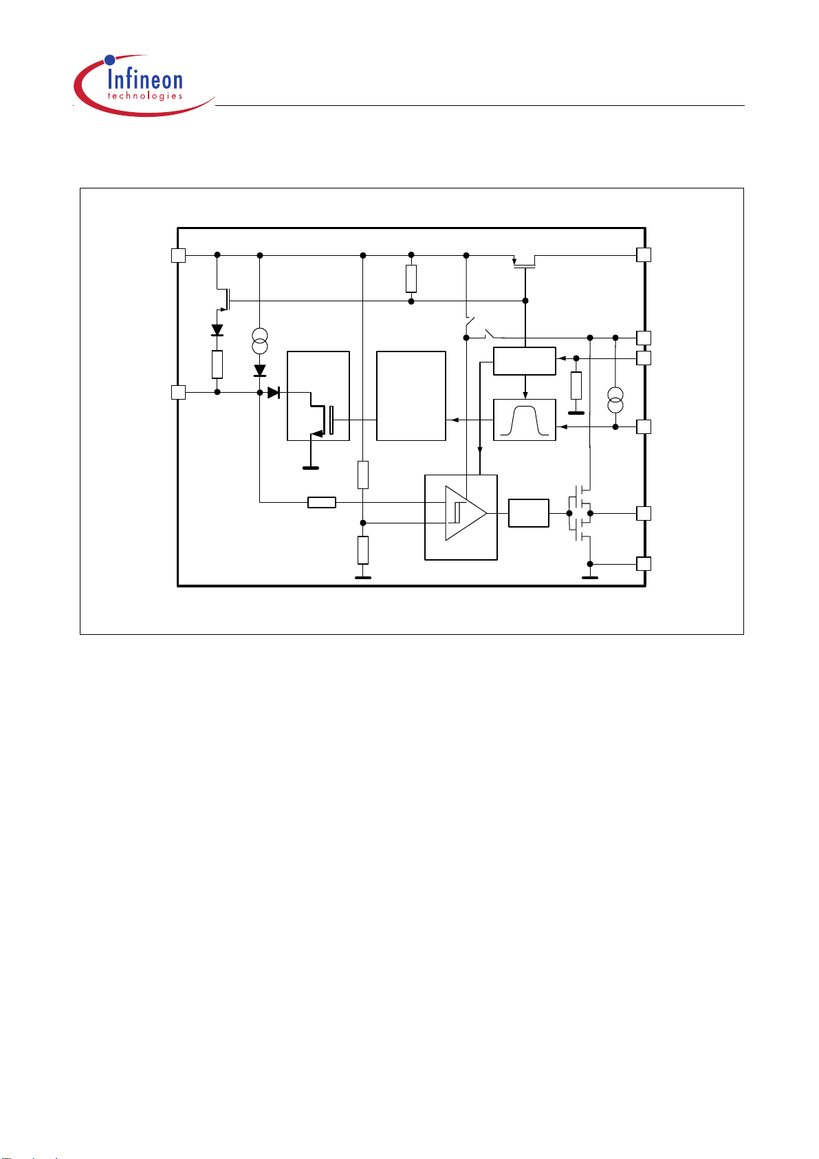
1.4 Functional Block Diagram
Final Datasheet TLE 6259-2
Figure 2
Vs
Bus
7
30 k
9
6
Output
Stage
Driver
Mode
Control
30 k
9
8
INH
3
Vcc
2
EN
Temp.-
Protection
Filter
4
TxD
1
RxD
Receiver
TLE 6259-2G
5
GND
Version 2.06 4 2003-02-21
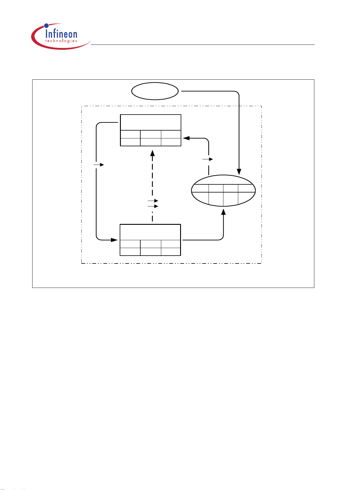
1.5 Application Information
Normal Mode
Final Datasheet TLE 6259-2
Start Up
Power Up
EN
high high
EN
low
EN
(V
high
CC
ON)
Sleep Mode
EN
low floating
1)
after wake-up via bus
2)
ON when INH not connected to voltage regulator
3)
after start up
INH
OFF
Figure 3: operation mode state diagram
VccINH
ON
V
CC
EN high
Stand-By
RxD
low
high
V
CC
1)
ON
3)
INH
EN
low high
2)
Wake Up
t > t
WAKE
Master Termination
For fail safe reasons, the TLE6259-2 already has a pull up resistor of 30kW implemented.
To achieve the required timings for the dominant to recessive transition of the bus signal
an additional external termination resistor of 1kW is required. It is recommended to place
this resistor in the master node. To avoid reverse currents from the bus line into the
battery supply line in case of an unpowered node, it is recommended to place a diode in
series to the external pull up. For small systems (low bus capacitance) the EMC
performance of the system is supported by an additional capacitor of at least 1nF in the
master node (see figure 6 and 7, application circuit).
External Capacitors
An capacitor of 22µF at the supply voltage input V
buffers the input voltage. In
S
combination with the required reverse polarity diode this prevents the device from
detecting power down conditions in case of negative transients on the supply line.
Version 2.06 5 2003-02-21

Final Datasheet TLE 6259-2
The 100nF capacitors close to the VS pins of the 6259-2 and the voltage regulator help
to improve the EMC behavior of the system.
Sleep Mode
In order to reduce the current consumption the TLE 6259-2 offers a sleep operation
mode. This mode is selected by switching the enable input EN low (see figure 3, state
diagram). In the sleep mode, a voltage regulator can be controlled via the INH output in
order to minimize the current consumption of the whole application. A wake-up caused
by a message on the communication bus, automatically enables the voltage regulator by
switching the INH output high. In parallel the wake-up is indicated by setting the RxD
output LOW. When entering the normal mode this wake-up flag is reset and the RxD
output is released to transmit the bus data.
In case the voltage regulator control input is not connected to INH output or the
microcontroller is active respectively, the TLE6259-2 can be set in normal operation
mode without a wake-up via the communication bus.
Bus Short to GND Feature
The TLE6259-2 also has a BUS short to GND feature implemented, in order to protect
the battery from running out of charge. A normal master termination connection like
described above, 1kW resistor and diode between bus and V
, whould cause a
S
constantly drawn current via this path. The resulting resistance of this short to GND is
lower than 1kW. To avoid this current during a generator off state, like a parked car, the
sleep mode has a bus short to GND feature implemented in the 6259-2. This feature is
only applicable, if the master termination is connected with the INH pin, instead of the
. For a more detailed information see the application circuit in figure 6 and 7.
V
S
Version 2.06 6 2003-02-21

Final Datasheet TLE 6259-2
2 Electrical Characteristics
2.1 Absolute Maximum Ratings
Parameter Symbol Limit Values Unit Remarks
min. max.
Voltages
Supply voltage
Battery supply voltage
Bus input voltage
Bus input voltage
V
V
Logic voltages at
V
V
V
EN, TxD, RxD
Input voltages at INH V
Output current at INH
Electrostatic discharge
I
V
voltage at Vs, Bus
Electrostatic discharge
V
voltage
Temperatures
Junction temperature
T
CC
S
bus
bus
I
INH
INH
ESD
ESD
j
-0.3 6 V
-0.3 40 V
-20 32 V
-20 40 V
-0.3 V
CC
+
V
t < 1s
0 V < VCC < 5.5 V
0.3
-0.3 VS +
V
0.3
20 mA
-4 4 kV
-2 2 kV
human body model
(100 pF via 1.5 kW)
human body model
(100 pF via 1.5 kW)
-40 150 °C–
Note: Maximum ratings are absolute ratings; exceeding any one of these values may cause
irreversible damage to the integrated circuit.
Version 2.06 7 2003-02-21

Final Datasheet TLE 6259-2
2.2 Operating Range
Parameter Symbol Limit Values Unit Remarks
min. max.
Supply voltage
Battery Supply Voltage
Junction temperature
V
V
T
CC
S
j
4.5 5.5 V
635V
– 40 150 °C
Thermal Resistances
Junction ambient
R
thj-a
–185K/W
Thermal Shutdown (junction temperature)
Symbol Limit Values Unit
min. typ. max.
Thermal shutdown temp.
T
Thermal shutdown hyst. D
jSD
T –10 –K
150 170 190 °C
–
–
Version 2.06 8 2003-02-21

2.3 Electrical Characteristics
Final Datasheet TLE 6259-2
4.5 V < VCC<5.5V; 6.0V<VS<27V; RL=500 W; VEN> V
to ground; positive current flowing into pin; unless otherwise specified.
; -40 °C < Tj< 125 °C; all voltages with respect
EN,ON
Parameter Symbol Limit Values Unit Remarks
min. typ. max.
Current Consumption
Current consumption
inNormal Mode
Current consumption
in Standby Mode
Current consumption
in Sleep Mode
I
I
I
I
I
I
CC
S
CC
S
CC
S
0.3 0,7 mA
0.4 0.8 mA
0.8 1.5 mA
1.3 2 mA
310µA
18 30 µA
--µA
18 30 µA
recessive state;
V
= V
TxD
dominant state;
V
TxD
recessive state,
without R
V
TxD
dominant state,
without R
V
TxD
external VR
activated INH=H
external VR
deactivated INH=L
CC
= 0 V
load
= V
CC
load
= 0 V
;
;
Version 2.06 9 2003-02-21

2.3 Electrical Characteristics (cont’d)
Final Datasheet TLE 6259-2
4.5 V < VCC<5.5V; 6.0V<VS<27V; RL=500 W; VEN> V
to ground; positive current flowing into pin; unless otherwise specified.
; -40 °C < Tj< 125 °C; all voltages with respect
EN,ON
Parameter Symbol Limit Values Unit Remarks
min. typ. max.
Receiver Output R´D
HIGH level output current
LOW level output current I
I
RD,H
RD,L
-1.2 -0.8 -0.5 mA
0.5 0.8 1.2 mA
VRD = 0.8 x VCC,
VRD = 0.2 x VCC,
Transmission Input T´D
HIGH level input voltage
V
threshold
TxD input hysteresis V
LOW level input voltage
V
threshold
TxD pull up current I
TD,H
TD,hys
TD,L
TD
2.9 0.7 x
V
CC
V
300 700 900 mV
0.3 x
V
CC
2.1 V
-150 -110 -70 µA
recessive state
dominant state
V
<0.3Vcc
TxD
Enable input (pin EN)
HIGH level input voltage
V
threshold
LOW level input voltage
V
threshold
EN input hysteresis V
EN pull down resistance R
Inhibit output (pin INH)
Inhibit R
resistance R
on
Leakage current I
EN,on
EN,off
EN,hys
EN
onINH
INH,lk
0.3 x
V
CC
2.8 0.7 x
V
CC
2.2 V
V
300 600 900 mV
15 30 60 kW
65 120 W
- 5.0 5.0 µA
normal mode
low power mode
I
= - 15 mA
INH
sleep mode;
V
= 0 V
INH
Version 2.06 10 2003-02-21

2.3 Electrical Characteristics (cont’d)
Final Datasheet TLE 6259-2
4.5 V < VCC<5.5V; 6.0V<VS<27V; RL=500 W; VEN> V
to ground; positive current flowing into pin; unless otherwise specified.
; -40 °C < Tj< 125 °C; all voltages with respect
EN,ON
Parameter Symbol Limit Values Unit Remarks
min. typ. max.
Bus receiver
Receiver threshold voltage,
V
recessive to dominant edge
Receiver threshold voltage,
V
dominant to recessive edge
Receiver hysteresis V
wake-up threshold voltage V
bus,rd
bus,dr
bus,hys
wake
0.44
x
V
S
0.02
x
V
S
0.40
x
V
S
0.5 x
V
S
0.56
x
V
S
0.04
x
V
S
0.5 x
V
S
0.6 x
V
S
0.1 x
V
S
0.6 x
V
S
V
V
mV
V
-8V<V
bus<Vbus,dom
V
bus,rec<Vbus
V
V
bus,hys
bus,rec
=
- V
Bus transmitter
<20 V
bus,dom
Bus recessive output voltage
V
Bus dominant output voltage V
Bus short circuit current I
Leakage current I
Bus pull up resistance R
Lin output current I
bus,rec
bus,dom
bus,sc
bus,lk
bus
lin
0.9 x
V
S
V
S
0.15
x
V
S
V
V
1.2 V
40 100 150 mA
-150 -70 mA
10 25 mA
10 µA
20 30 47 kW
53060µA
V
V
8V<V
6V<VS<8V
V
VCC=0V, VS=0V,
V
VCC=0V, VS=0V,
V
V
Normal mode
Sleep mode
= V
TxD
= 0 V;
TxD
S
bus,short
= -8 V
bus
= 20 V
bus
LIN=VS
CC
<27V
= 13.5 V
=13,5V
Version 2.06 11 2003-02-21

2.3 Electrical Characteristics (cont’d)
Final Datasheet TLE 6259-2
4.5 V < VCC<5.5V; 6.0V<VS<27V; RL=500 W; VEN> V
to ground; positive current flowing into pin; unless otherwise specified.
; -40 °C < Tj< 125 °C; all voltages with respect
EN,ON
Parameter Symbol Limit Values Unit Remarks
min. typ. max.
Dynamic Transceiver Characteristics
Slope fall time
Slope rise time
Slope symmetry t
Slope fall time t
Slope rise time
Slope symmetry t
Propagation delay
t
fslope
t
rslope
slopesym
fslope
t
rslope
slopesym
t
d(L),T
22,5 µs
22,5 µs
-5 5 µs
22.5 µs
22.5 µs
-4 4 µs
13µs
100% > V
C
bus
V
CC
0% > V
C
bus
V
CC
t
fslope
100% > V
C
bus
T
ambient
V
CC
0% > V
C
bus
V
CC
t
fslope
VCC = 5 V
bus
= 10 nF; RL=500W
= 5 V; VS = 13.5 V
>10 0%
bus
= 10 nF; RL=500W
= 5 V; VS = 13.5 V
t
rslope
-
bus
= 6,8nF;RL=660W
<85°C;
= 5 V; VS = 13.5 V
>100%
bus
= 6,8nF;RL=660W
= 5 V; VS = 13.5 V
t
rslope
-
TxD LOW to bus
> 0%
> 0%
Propagation delay
TxD HIGH to bus
Propagation delay
bus dominant to RxD LOW
Propagation delay
bus recessive to RxD HIGH
Receiver delay symmetry t
Transmitter delay symmetry t
Wake-up delay time t
Delay time for change sleep/
stand by mode-normal mode
Delay time for change normal
mode - sleep mode
t
d(H),T
t
d(L),R
t
d(H),R
sym,R
sym,T
wake
t
snorm
t
nsleep
13µs
16µs
16µs
-2 2 µs
-2 2 µs
30 100 150 µs
170 µs
10 µs
10 µs
VCC = 5 V
VCC = 5V;
C
= 20pF
RxD
VCC = 5 V;
C
= 20 pF
RxD
t
= t
sym,R
t
sym,T
Tj £ 125°
Tj £ 150°
= t
d(L),R
d(L),T
- t
- t
d(H),R
d(H),T
Version 2.06 12 2003-02-21

3 Diagrams
Final Datasheet TLE 6259-2
1 k
9
Figure 4: Test circuits
100 nF
C
bus
Vs
Bus
GND
EN
INH
TxD
RxD
V
CC
20 pF
100 nF
V
V
V
TxD
bus
RxD
V
GND
GND
V
GND
CC
0.7*V
t
t
CC
t
0.3*V
t
d(H),T
V
bus,dr
t
d(H),R
CC
t
d(H),TR
t
t
d(L),TR
d(L),T
t
d(L),R
V
bus,rd
V
S
CC
Figure 5: Timing diagrams for dynamic characteristics
Version 2.06 13 2003-02-21

4 Application
V
LIN bus
bat
Final Datasheet TLE 6259-2
master node
TLE 6259-2G
Vs
EN
1 k
1nF
22 µF
slave node
100 nF
100 nF
100 nF
Bus
INH
GND
INH
e.g. TLE 4263
V
I
GND
TLE 6259-2G
Vs
RxD
TxD
V
V
EN
RxD
CC
Q
100 nF
µP
GND
100 nF
5V
22 µF
ECU 1
µP
GND
22 µF
100 nF
Bus
INH
GND
V
I
e.g. TLE 4278
GND
TxD
V
V
CC
100 nF
Q
100 nF
5V
22 µF
ECU X
Figure 6
Application circuit with bus short to GND feature applied
Version 2.06 14 2003-02-21

V
bat
LIN bus
master node
Final Datasheet TLE 6259-2
TLE 6259-2G
Vs
EN
1 k
1nF
22 µF
slave node
100 nF
100 nF
100 nF
Bus
INH
GND
INH
e.g. TLE 4263
V
I
GND
TLE 6259-2G
Vs
RxD
TxD
V
CC
100 nF 100 nF
V
EN
RxD
5V
Q
µP
GND
22 µF
ECU 1
µP
GND
22 µF
100 nF
Bus
INH
GND
V
I
e.g. TLE 4278
GND
TxD
V
V
CC
Q
100 nF
100 nF
5V
22 µF
ECU X
Figure 7
Application circuit without bus short to GND feature
Version 2.06 15 2003-02-21

5 Package Outlines
P-DSO-8-3
(Plastic Dual Small Outline Package)
0.1 MIN.
(1.5)
0.33
1.75 MAX.
Final Datasheet TLE 6259-2
±0.08
x 45˚
1)
4
-0.2
1
+0.05
-0.0
MAX.8˚
0.2
0.41
1.27
+0.1
-0.05
0.1
0.2MA
8
5
C
C
x8
Index
Marking
4
1
1)
5
-0.2
A
Index Marking (Chamfer)
1)
Does not include plastic or metal protrusion of 0.15 max. per side
Sorts of Packing
Package outlines for tubes, trays etc. are contained in our
Data Book “Package Information”.
6
±0.2
0.64
±0.25
SMD = Surface Mounted Device
Dimensions in mm
Version 2.06 16 2003-02-21

Final Datasheet TLE 6259-2
Edition 1999-10-12
Published by Infineon Technologies AG
St.-Martin-Strasse 53
D-81541 München
© Infineon Technologies AG1999
All Rights Reserved.
Attention please!
The information herein is given to describe certain components and shall not be considered as warranted characteristics.
Terms of delivery and rights to technical change reserved.
We hereby disclaim any and all warranties, including but not limited to warranties of non-infringement, regarding circuits, descriptions and
charts stated herein.
Infineon Technologies is an approved CECC manufacturer.
Information
For further information on technology, delivery terms and conditions and prices please contact your nearest Infineon Technologies Office
in Germany or our Infineon Technologies Representatives worldwide (see address list).
Warnings
Due to technical requirements components may contain dangerous substances. For information on the types in question please contact
your nearest Infineon Technologies Office.
Infineon Technologies Components may only be used in life-suppor t devices or systems with the express written approval of Infineon Technologies, if a failure of such components can reasonably be expected to cause the failure of that life-support device or system, or to affect
the safety or effectiveness of that device or system. Life suppor t devices or systems are intended to be implanted in the human body, or to
support and/or maintain and sustain and/or protect human life. If they fail, it is reasonable to assume that the health of the user or other
persons may be endangered.
Version 2.06 17 2003-02-21

Infineon goes for Business Excellence
“Business excellence means intelligent approaches and clearly
defined processes, which are both constantly under review and
ultimately lead to good operating results.
Better operating results and business excellence mean less
idleness and wastefulness for all of us, more professional
success, more accurate information, a better overview and,
thereby, less frustration and more satisfaction.”
Dr. Ulrich Schumacher
http://www.infineon.com
Published by Infineon Technologies AG
 Loading...