

现货库存、技术资料、百科信息、热点资讯,精彩尽在鼎好!
Tracking Regulator
Features
• Output tracking tolerance to reference ≤ ±0.2%
• Output voltage adjust down to 1.5 V
• 250 mA output current capability
• Enable function
• Very low current consumption in OFF mode
• Wide operation range: up to 40 V
• Wide temperature range: -40 °C ≤
• Output protected against short circuit to GND and
Battery
• Overtemperature protection
• Reverse polarity proof
T
≤ 150 °C
j
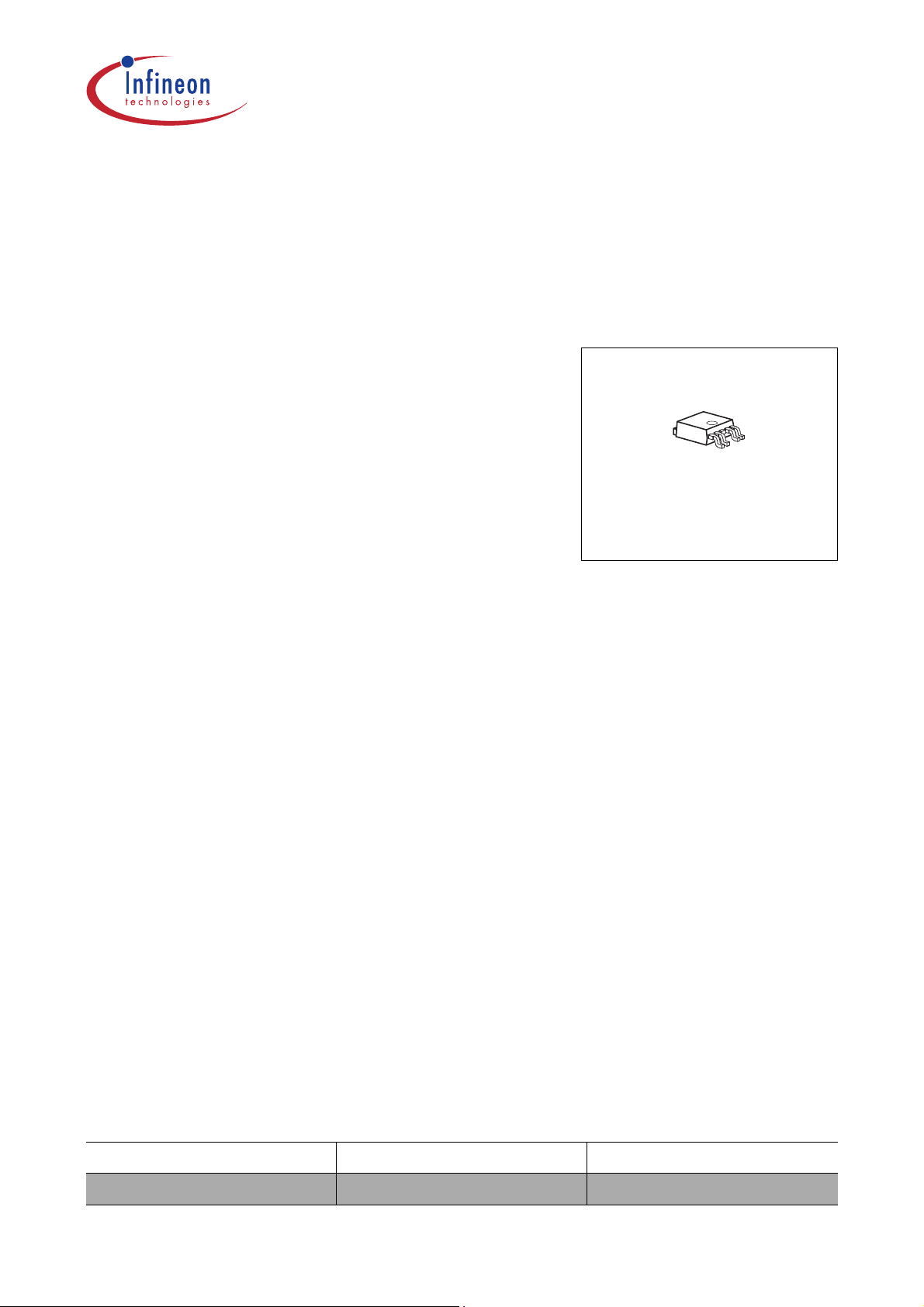
TLE 4252
P-TO252-5-1
Short Functional Description
The TLE 4252 is a monolithic integrated low -drop voltage tracking regulator in a very
small SMD package P-TO252-5-1. It is designed to supply off-board systems, e.g.
sensors in engine management systems under the severe conditions of automotive
applications. Therefore the device is equipped with additional protection functions
against reverse polarity and short circuit to GND and battery.
With supply voltages up to 40 V the output voltage follows a reference voltage applied at
the adjust input with h igh acc uracy. Th e referenc e volta ge appli ed direc tly to the adjust
input or by an e.g. external resistor divider can be 1.5 V at minimum.
The output is able to drive loads up to 250 mA at minimum while they follow e.g. the 5 V
output of a main voltage regulator as reference with high accuracy.
The TLE 4252 tracker can be switched into stand-by mode to reduce the current
consumption to very low values. This feature makes the IC suitable for low power battery
applications.
Type Ordering Code Package
TLE 4252 D Q67006-A9669 P-TO252-5-1
Data Sheet 1 Rev. 1.2, 2004-08-11
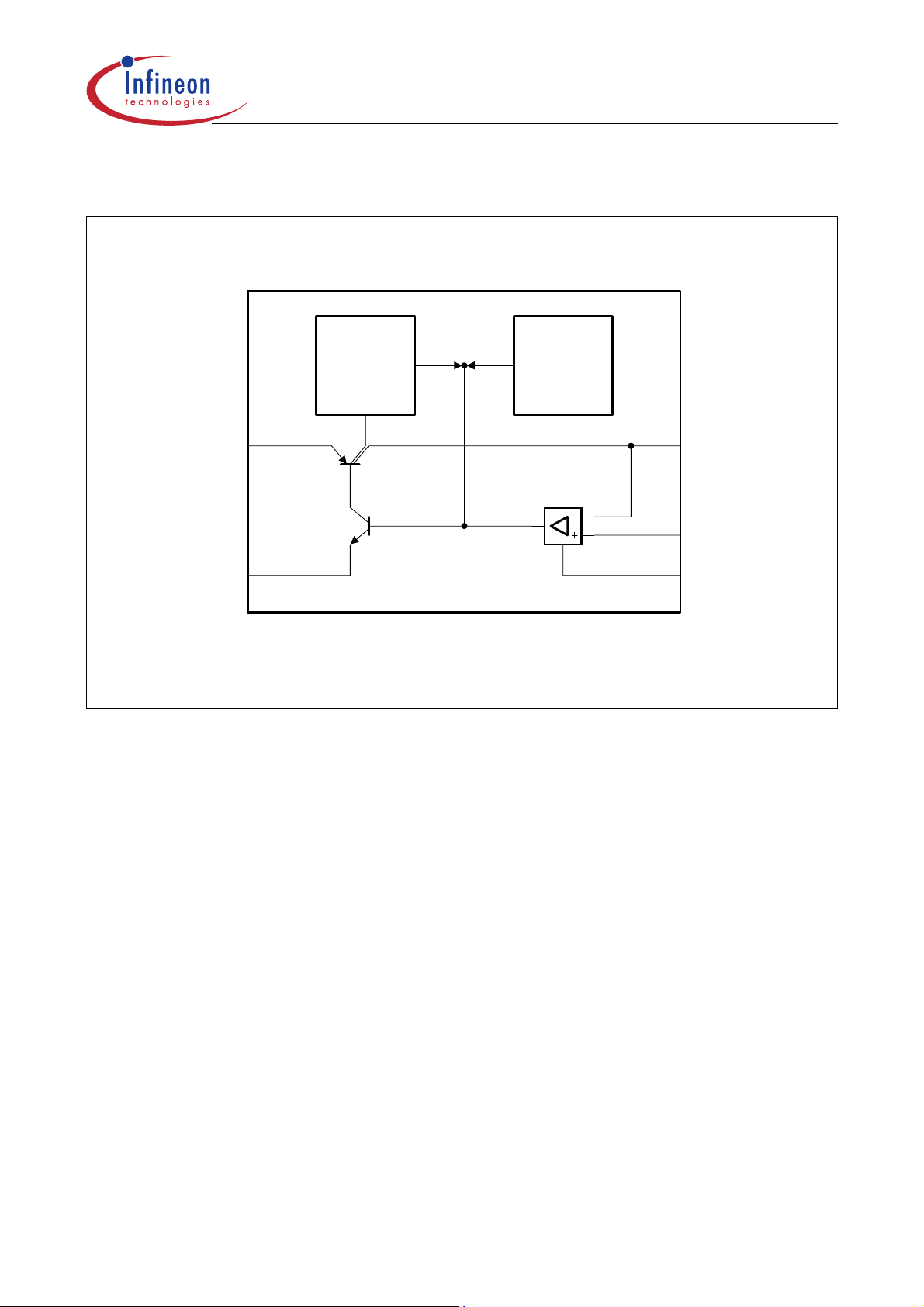
Block Diagram
Saturation
Control and
Protection
Circuit
TLE 4252
Temperature
Control
I
GND EN
Figure 1 Internal Circuit Blocks
Q
ADJ
TLE 4252 D
AEB03536.VSD
Data Sheet 2 Rev. 1.2, 2004-08-11
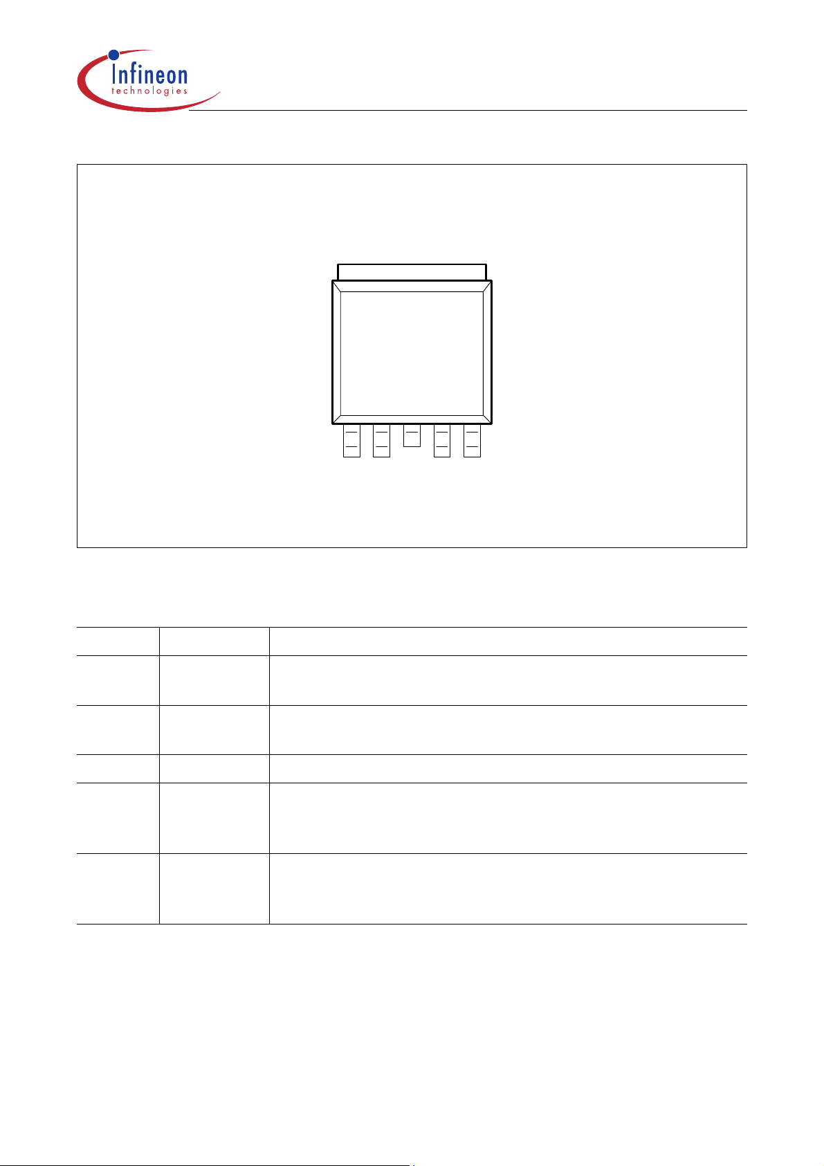
TLE 4252
TLE 4252
(P-TO252-5-1 D-Pak)
GND
1
2
I
EN
4
3
ADJ
GND
AEP03534.VSD
5
Q
Figure 2 Pin Configuration (Draft, subject to alternation!)
Table 1 Pin Definitions and Functions (draft, subject to alternation)
Pin No. Symbol Function
1I Supply voltage input; Input for battery or a pre-regulated
voltage of a e.g. DC to DC converter.
2EN Enable input for tracker; An active high signal turns on the
device, with active low the tracker is turned off.
3GNDGround; Connected to the heatsink of the package.
4ADJAdjust input for tracker; Input for the reference voltage
which can be connected directly or by voltage divider to the
reference (see Application Information).
5Q Output voltage of tracker; For a stable operation to avoid
ringing at the output connect a capacitor of
C
≥ 10 µF and
Q
0 ≤ ESR ≤ 5 Ω to GND.
Data Sheet 3 Rev. 1.2, 2004-08-11
Table 2 Absolute Maximum Ratings
Parameter Symbol Limit Values Unit Remarks
Min. Max.
Supply Voltage Input I
TLE 4252
Voltage
Current
Enable Input EN
Voltage
Current
Adjust Input ADJ
Voltage
Current
Output Q
Voltage
Current
Temperature
Junction temperature
Storage temperature
ESD-Protection
V
I
V
I
V
I
V
I
T
T
I
I
EN
EN
ADJ
ADJ
Q
Q
j
stg
-42 45 V –
– – A Limited internally
-42 45 V –
– – A Limited internally
-42 45 V –
– – A Limited internally
-2 45 V –
– – A Limited internally
-40 150 °C–
-50 150 °C–
Voltage
V
ESD
-2 2 kV Human Body Model
(HBM)
Note: Maximum ratings are absolute ratings, exceeding one of these values may cause
irreversible damage to the integrated circuit!
Data Sheet 4 Rev. 1.2, 2004-08-11

Table 3 Operating Range
Parameter Symbol Limit Values Unit Remarks
Min. Typ. Max.
In- and Output Voltage
TLE 4252
Supply voltage
Enable input voltage V
Adjust input voltage
Adjust input voltage
Error amplifier
common mode range
V
V
V
I
EN
ADJ
ADJ
3.5 – 40 V VI > V
0–40V–
1.5 – 40 V –
0–1.5VVQ ≤ V
CMR 1.5 – V
0.5
I
-
V VQ ≤ V
V
= V
FB
+ V
ADJ
+ ∆V
ADJ
+ ∆VQ with
ADJ
Q
dr
Q
Temperature
Junction temperature
T
j
-40 – 150 °C–
Thermal Resistance P-TO252-5-1
Junction to ambient
Junction to ambient R
Junction to ambient R
Junction to case R
1) Worst case regarding peak temperature; zero airflow; mou nt ed on FR4; 80 × 80 × 1.5 mm3; 35 µ Cu; 5 µ Sn
R
thj-a
thj-a
thj-a
thj-c
– – 144 K/W Footprint only
– – 78 K/W Heat sink area
300 mm
2 1)
– – 55 K/W Heat sink area
600 mm
2 1)
––2K/W–
1)
Note: Within this operating range the IC is functional. The electrical characteristics,
however, are not guaranteed over this full range given above.
Data Sheet 5 Rev. 1.2, 2004-08-11

TLE 4252
Table 4 Electrical Characteristics
V
= 13.5 V; 1.5 V ≤ V
I
Parameter Symbol Limit Values Unit Test Condition
Regulator Performance, Tracker Output Q
≤ VI - 0.6 V; -40 °C < Tj < 150 °C; unless otherwise specified
ADJ
Min. Typ. Max.
Output voltage
∆V
tracking accuracy
∆
V
= V
Q
Output voltage
ADJ
- V
Q
∆V
tracking accuracy
V
= V
∆
Q
Drop voltage
ADJ
- V
Q
V
Output current I
Output capacitor C
Current consumption
I
= II - I
q
Q
Current consumption
I
= II - I
q
Q
I
I
Q
Q
dr
Q
Q
-10 – 10 mV 4.5 V < VI < 26 V;
I
1 mA <
< 200 mA;
Q
-10 – 10 mV 3.5 V < VI < 32 V;
I
10 mA <
-25 – 25 mV 3.5 V <
1 mA <
< 100 mA;
Q
V
< 4.5 V;
I
I
< 200 mA;
Q
– 280 600 mV IQ = 200 mA;
V
> 3.5 V;
ADJ
V
= V
EN
250 350 500 mA VQ = 5.0 V
1)
EN, on
2)
10 – – µF0 ≤ ESR ≤ 5 Ω at
10 kHz
q
q
– 1025mAIQ = 200 mA;
V
= 5 V
Q
– 100 150 µA IQ < 100 µA;
T
< 85 °C; VEN = 5 V
j
Quiescent current
(stand-by)
I
= II - I
q
Q
Reverse current
Load regulation ∆
Line regulation ∆
Power supply ripple
rejection
Data Sheet 6 Rev. 1.2, 2004-08-11
I
q
I
r
V
Q
V
Q
–02µA VEN = 0 V;
–0.55mAVQ = 16 V; VI = 0 V
– – 10 mV 1 mA < IQ < 200 mA
– – 10 mV 5 V < VI < 32 V;
PSSR –60–dBf
V
EN/ADJ
T
< 85 °C
j
I
= 5 mA
Q
I, ripple
V
I, ripple
= 0 V;
= 100 Hz;
= 0.5 Vpp
3)

TLE 4252
Table 4 Electrical Characteristics (cont’d)
V
= 13.5 V; 1.5 V ≤ V
I
Parameter Symbol Limit Values Unit Test Condition
Adjust Input ADJ
≤ VI - 0.6 V; -40 °C < Tj < 150 °C; unless otherwise specified
ADJ
Min. Typ. Max.
Input biasing current
I
ADJ
–0.10.5µA V
ADJ
= 5 V
Enable Input EN
Device on voltage
V
EN, on
2.0 – 40 V VQ settled
range
Device off voltage
V
EN, off
0–0.8VVQ < 0.1 V
range
Input current
EN pull-down resistor
1) Measured when the outpu t volt age VQ has dropped 100 mV from the no m inal value.
2) The current limit depends also on the input voltage, see graph output current vs. input voltage in the diagrams
section.
3) Specified by design. Not subject to production test.
I
R
EN
EN
-1 2 5 µA VEN = 5 V
–1.5–MΩ –
Data Sheet 7 Rev. 1.2, 2004-08-11

Application Information
V
BAT
Main µC Supply
I
TLE 4271-2
TLE 4278
TLE 4470
e.g.
etc.
TLE 4252
Q
R
1ADJ
V
DD
µC
e.g. C167
GND
R
2ADJ
4
1
I
I/O
EN
TLE 4252 D
GND
V
< V
Q
5
QADJ
AEA03535.VSD
REF
Figure 3 Application Circuit: Output Voltage < Reference Voltage
Figure 3 shows a typical application circuit with
< V
Q
. Of course, also VQ = V
REF
REF
is
V
feasible by directly connecting the reference pin of the TLE 4252 D to the appropriate
voltage level without voltage divider.
The output voltage calculates to:
R
1ADJ
2ADJ
R
+
(1)
2ADJ
V
V
Q
REF
------------------------------------
×=
R
Data Sheet 8 Rev. 1.2, 2004-08-11

Diagrams
TLE 4252
Output Current Limit
Input Voltage
500
mA
I
Q1,2
400
300
200
100
0
V
I
T
= 25°C
j
0
10 20 30 40 50
I
versus
Q
AED03537.VSD
V
V
I1,2
Data Sheet 9 Rev. 1.2, 2004-08-11

Package Outlines
TLE 4252
+0.15
6.5
-0.10
B
±0.1
1
0...0.15
0.51 min
-0.2
±0.5
6.22
9.9
0.15 max
per side
±0.1
1
(4.17)
5.4
±0.1
±0.15
0.8
5x0.6
A
±0.1
1.14
4.56
M
B
A0.25
All metal surfaces tin plated, except area of cut.
2.3
+0.05
-0.10
0.9
0.5
GPT09161
+0.08
-0.04
+0.08
-0.04
0.1
Figure 4 P-TO252-5-1 (Plastic Transistor Single Outline)
You can find all of our packages, sorts of packing and others in our
Infineon Internet Page “Products”: http://www.infineon.com/products.
SMD = Surface Mounted Device
Dimensions in mm
Data Sheet 10 Rev. 1.2, 2004-08-11

Edition 2004-08-11
Published by Infineon Technologies AG,
St.-Martin-Strasse 53,
81669 München, Germany
© Infineon Technologies AG 2004.
All Rights Reserved.
Attention please!
The information herein is given to descr ibe certain com ponents and shall not be considered as a guarantee of
characteristics.
Terms of delivery and rights to technical change reserved.
We hereby disclaim any and all warranties, including but not limited to warranties of non-infringement, regarding
circuits, descriptions and charts stated herein.
Information
For further information on tech nology, delivery terms and conditions and prices please contact your nearest
Infineon Technologies Office (www.infineon.com).
Warnings
Due to technical requirements co mponents may contain dangerous substances. For information on the types in
question please contact your neares t Infineon Technologies Office.
Infineon Technologies Components may only be used in life-support devices or systems with the express written
approval of Infineon T echnologies, if a f ailure of such components can reasonably be expected to cause the failure
of that lif e -su pp o rt de vi ce o r system, or to affect the safety or effecti veness of that device o r system. Life support
devices or systems are inten ded to be implante d in the human body, or to support and/or maintain and sustain
and/or protect human life. If they fail, it is reasonable to assume that the health of the user or other persons may
be endangered.
 Loading...