

LED Driver with Adjustable Current
TLE 4241 GM
Features
• Adjustable constant output current
• Wide input voltage range
• Low drop voltage
• Open load detection
• Overtemperature protection
• Short circuit proof
• Reverse polarity proof
T
• Wide temperature range: -40 °C <
< 150 °C
j
• Very small SMD-Package
Functional Description
The TLE 4241 GM is an integrated adjustable constant current source. It provides an
output current adjustable via different means (SET, PWM, reference resistor) which is
kept nearly independent from load and supply voltage changes. The IC is designed to
supply LEDs under the severe conditions of automotive applications resulting in constant
brightness and extended LED lifetime. It is provided in the very small P-DSO-8-9
(Micro 8) package. Protection circuits prevent damage to the device in case of overload,
short circuit, reverse polarity and overtemperature. The connected LEDs are pr otected
against reverse polarity as well as excess voltages up to 45 V. A status output allows
handling of open load and short circuit at the main output.
A PWM input offers the possibility to adjust the LED brightness by pulse width
modulation.
With an implemented high/low current switch the output current level can be reduced e.g.
for brake/tail light application.
The implemented features such as adjustable output current, the high/low current switch
and the provided PWM input make the device well suited for a broad ran ge of LED an d
other applications.
P-DSO-8-3, -6, -7, -8, -9
Type Ordering Code Package
TLE 4241 GM Q67006-A9644 P-DSO-8-9
Data Sheet 1 Rev. 1.2, 2004-04-13
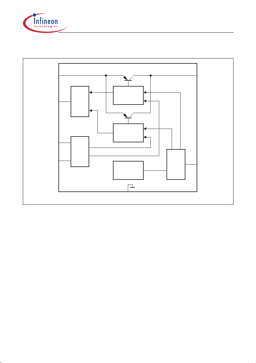
Circuit Description
TLE 4241 GM
Q
REF
AEB03003
ST
PWM
SET
I
Regulation
High
Status
Regulation
Low
Control
Reference
Voltage
GND
V/I Converter
Figure 1 Block Diagram
An internal reference voltage of typ. 1.20 V supplies the REF pin which is connected to
GND via an external resistor. In the SET = H mode the reference current flowing on the
REF pin is mirrored with an amplification to form the desired output current. The typ.
output current in the SET = H mode calculates:
1.20
I
/mA
Qtyp,
----------------------
R
REF
/kΩ
487 0.1+×=
(1)
The output current is shown as a function of the reference resistance on Page 10 for the
high as well as for the low current mode.
With the PWM input the LED brightness can be regulated via duty cycle. Also PWM = L
sets the TLE 4241 in sleep mode resulting in a very low current consumption of << 1 µA
I
typ. Due to the high impedance of the PWM input (see timing diagram
PWM
versus V
PWM
on Page 12) the PWM pin can thus also be used as an Enable input.
Data Sheet 2 Rev. 1.2, 2004-04-13
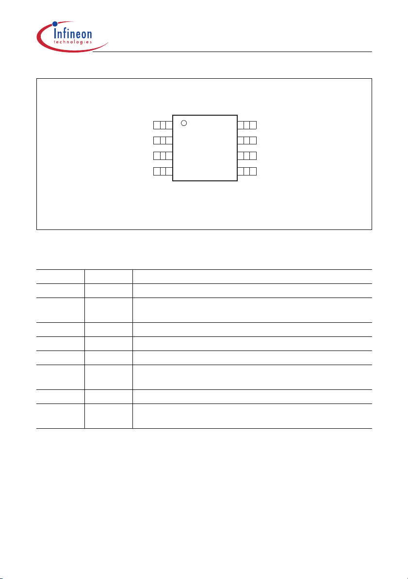
TLE 4241 GM
81GND
I
ST 2 7
PWM 3 6
SET 4 5
Figure 2 Pin Configuration (top view)
Table 1 Pin Definitions and Functions
Pin No. Symbol Function
1GNDGround; internally connected to pin 5
2STStatus Output; open collector output, connect to external
pull-up resistor (10 kΩ or higher)
3PWMPulse Width Modulation Input; if not needed connect to
4 SET High/Low Current Input; choice of current level
5GNDGround; internally connected to pin 1
6REFReference Input; connect to GND via an external resistor to
adjust the output current
7QOutput
8IInput; block to GND directly at the IC with a 100 nF ceramic
capacitor
Q
REF
GND
AEP03002
V
I
Data Sheet 3 Rev. 1.2, 2004-04-13
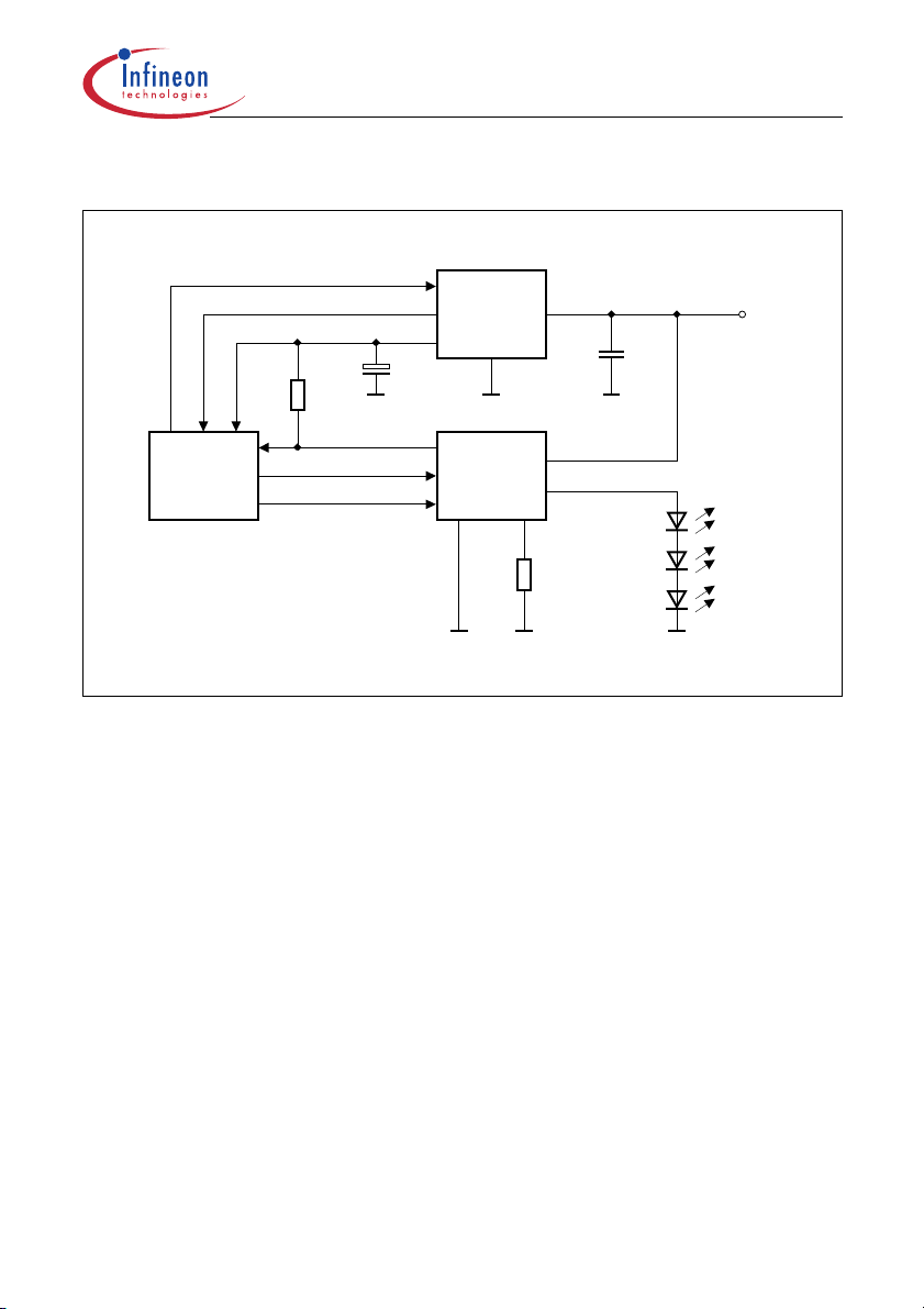
Application Information
µC
V
Q
WD R
10 k
TLE 4241 GM
W
RO
TLE 4271
22 µF
Ω
ST
PWM
SET
TLE 4241G
I
Q
R
REF
100 nF
V
Batt
LA E67B
OSRAM
AED03098
Figure 3 Application Circuit
Figure 3 shows a typical application with the TLE 4241 GM LED driver. The 3 LEDs are
driven with an adequate supply current adjusted by the resistor R
. Thus brightness
REF
variations due to forward voltage spread of the LEDs are prevented. The lumi nosity
spread arising from the LED production process can be compensated via software by an
appropriate duty cycle applied to the PWM pin. Hence selection of the LEDs to forward
voltage as well as to luminosity classes can be spared. The slightly negative temperature
coefficient of the TLE 4241 GM output current protects the LEDs against overtemperature stress if the IC is placed nearby the LEDs.
V
The voltage drop (
- VQ) across the TLE 4241 GM is monitored in order to detect an
I
open load condition indicated at the status ou tput pin ST. In case of open load, the
voltage drop will decrease below the lower status switching threshold V
. Hence, the
dr,L
status output ST will be driven low. In normal operation , the voltage drop is above the
V
upper status threshold
, thus the open collector output ST is in high-ohmic state (see
dr,H
also section Status Output at the Electrical Characteristics).
The function of ST, SET and PWM as well as their timings are shown in Figure 4.
Data Sheet 4 Rev. 1.2, 2004-04-13
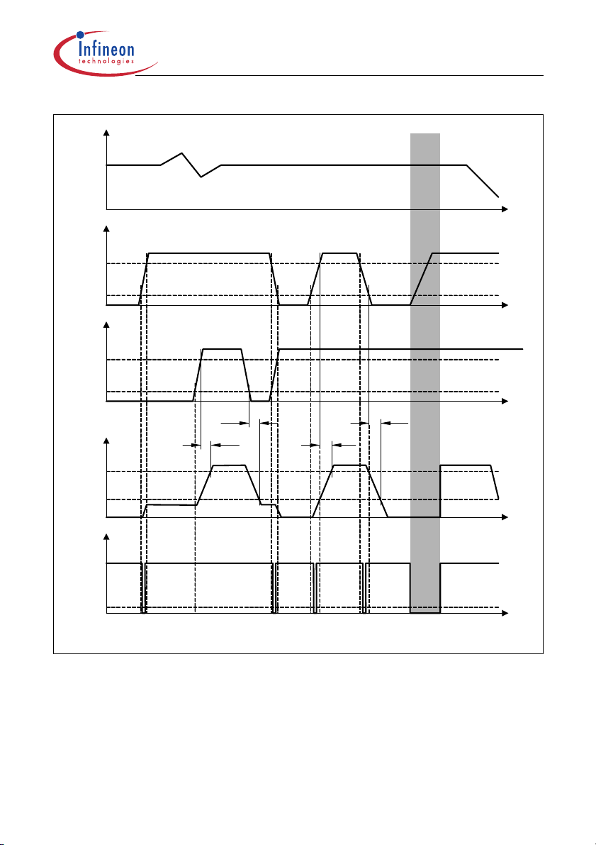
TLE 4241 GM
V
I
V
V
PWM, H
V
V
V
PWM
PWM, L
V
SET
SET, H
SET, L
I
mA
V
ST
V
STL
t
t
t
SET, L
t
Q
SET, H
t
PWM, ON
t
PWM, OFF
47
10
t
t
Open Load
t
AET03339.VSD
Figure 4 Function and Timing Diagram
Data Sheet 5 Rev. 1.2, 2004-04-13

TLE 4241 GM
Table 2 Absolute Maximum Ratings
-40 °C < Tj < 150 °C
Parameter Symbol Limit Values Unit Remarks
Min. Max.
Input
Voltage V
Current
I
I
I
Output
Voltage V
Current
Q
I
Q
Status Output
Voltage V
Current
ST
I
ST
Reference Input
Voltage V
Current
I
REF
REF
Pulse Width Modulation Input
Voltage V
PWM
Current – -1 1 mA –
High/Low Current Input
Voltage
Current
V
I
SET
SET
Temperatures
Junction temperature T
Storage temperature
j
T
stg
Thermal Resistances
Junction ambient R
1) Worst case regarding peak temperature; mounted on PCB 80 × 80 × 1.5 mm3, 35 µm Cu, 300 mm2 heat sink
area.
thja
-42 45 V –
– – mA internally limited
-1 40 V –
– – mA internally limited
-0.3 40 V –
– 5 5 mA internally limited
-0.3 7 V –
-2 2 mA –
-40 40 V –
-40 40 V –
-1 1 mA –
-40 150 °C–
-50 150 °C–
– 105 K/W
1)
Note: Maximum ratings are absolute ratings; exceeding any one of these valu es may
cause irreversible damage to the integrated circuit.
Data Sheet 6 Rev. 1.2, 2004-04-13

TLE 4241 GM
Table 3 Operating Range
Parameter Symbol Limit Values Unit Remarks
Min. Max.
Input voltage
Status output voltage
SET voltage
PWM voltage
Junction temperature
Reference Resistor
V
V
V
V
T
R
I
ST
SET
PWM
j
REF
445V–
–16V–
040V–
040V–
-40 150 °C–
7100kΩ SET = H
4.7 18 kΩ SET = L
Data Sheet 7 Rev. 1.2, 2004-04-13

TLE 4241 GM
Table 4 Electrical Characteristics
V
9V ≤
≤ 16 V; R
I
respect to ground; positive current defined flowing into pin; unless otherwise specified
Parameter Symbol Limit Values Unit Test Condition
Current consumption off
mode
Current consumption
Current consumption
Current consumption
open load
Current consumption
open load
Output
Output current
Output current
Current Ratio
Output current limit
Output current limit
Drop voltage
Drop voltage V
PWM Input
PWM high level
PWM low level
PWM input current
high level
PWM input current
low level
Turn on delay time
= 10 kΩ; V
REF
I
qOFF
I
qL
I
qH
I
qL,O
I
qH,O
I
Q
I
Q
I
QH/IQL
I
Qmax
I
Qmax
V
dr
dr
V
PWM,H
V
PWM,L
I
PWM,H
I
PWM,L
t
PWM,ON
PWM
≥ V
; -40 °C < Tj < 150 °C; all voltages with
PWM,H
Min. Typ. Max.
–0.12µA PWM = L, TJ < 85 °C;
V
≤ 13.5 V
I
– 5 10 mA SET = L; VQ = 6 V
– 6 10 mA SET = H; VQ = 6 V
– – 10 mA SET = L; VQ open
– – 10 mA SET = H; VQ open
6.7 8.4 10 mA SET = L, VQ = 6 V
V
–8.6–mASET = L,
= 4 V
Q
47 58.5 70 mA SET = H, VQ = 6 V
– 60.0 – mA SET = H,
V
Q
678––
– 83 – mA SET = L; R
– 83 – mA SET = H; R
REF
REF
– 0.2 0.5 V SET = L;
I
= 80% of I
Q
– 0.3 0.5 V SET = H;
I
= 80% of I
Q
2.0 – – V –
––0.5V–
– 220 500 µA V
-10 – 10 µA V
PWM
PWM
= 5.0 V
= 0.0 V
0530µs 20%/80% IQ, see
Figure 4
= 4 V
= 0 Ω
= 0 Ω
Q,nom,L
Q,nom,H
Data Sheet 8 Rev. 1.2, 2004-04-13

TLE 4241 GM
Table 4 Electrical Characteristics (cont’d)
V
9V ≤
≤ 16 V; R
I
respect to ground; positive current defined flowing into pin; unless otherwise specified
Parameter Symbol Limit Values Unit Test Condition
Turn off delay time t
SET Input
SET high level V
SET low level
SET input current
high level
SET input current
low level
Delay time L -> H
Delay time H -> L
Status Output
Lower status switching
threshold
Upper status switching
threshold
Status low voltage
Leakage current
= 10 kΩ; V
REF
PWM,OFF
SET,H
V
SET,L
I
SET,H
I
SET,L
t
SET,H
t
SET,L
V
dr,L
V
dr,H
V
STL
I
STLK
PWM
≥ V
; -40 °C < Tj < 150 °C; all voltages with
PWM,H
Min. Typ. Max.
01030µs 20%/80% IQ, see
Figure 4
2.0 – – V –
––0.5V–
– 220 500 µA V
-10 – 10 µA V
SET
SET
= 5.0 V
= 0.0 V
––30µs 20%/80% IQ, see
Figure 4
––30µs 20%/80% IQ, see
Figure 4
0.15 – – V (VI - VQ) decreasing
SET = L
V
0.15 – – V (
- VQ) decreasing
I
SET = H
––0.7V(VI - VQ) increasing
SET = L
V
––0.7V(
- VQ) increasing
I
SET = H
––0.4V(VI - VQ) < V
I
= 1.0 mA
ST
––10µA(VI - VQ) > V
V
= 5.0 V
ST
dr,L
dr,H
Data Sheet 9 Rev. 1.2, 2004-04-13

Typical Performance Characteristics
Output Current versus
External Resistor, SET = H
100
mA
I
Q
80
70
60
50
40
30
20
10
0
5
10 20 50 100
AED03333.VSD
SET = H
V
= 6 V
Q
k
Ω
R
REF
Output Current versus
External Resistor, SET = L
20
mA
I
Q
16
14
12
10
8
6
4
2
0
5
10 20 50 100
TLE 4241 GM
AED03334.VSD
SET = L
V
= 6 V
Q
k
Ω
R
REF
Output Current versus
Supply Voltage, SET = H
100
mA
I
Q
80
70
60
50
40
30
20
10
0
0
5 1015202530 40
Data Sheet 10 Rev. 1.2, 2004-04-13
AED03335.VSD
V
= 6 V
Q
R
= 10 kΩ
REF
SET = H
V
V
I
Output Current versus
Supply Voltage, SET = L
20
mA
I
Q
16
14
12
10
8
6
4
2
0
0
5 1015202530 40
AED03336.VSD
V
= 6 V
Q
R
= 10 kΩ
REF
SET = L
V
V
I

Reference Voltage versus
Junction Temperature
1.25
V
V
REF
1.23
1.21
1.19
1.17
1.15
-40
0 40 80 °C 160
AED03340.VSD
R
= 10 kΩ
REF
TLE 4241 GM
T
j
Data Sheet 11 Rev. 1.2, 2004-04-13

TLE 4241 GM
PWM Pin Input Current versus
PWM Voltage
AED03332.VSD
I
PWM
2.0
mA
1.5
1.0
0.5
0
0
5 1015202530 V40
SET Pin Input Current versus
SET Voltage
2.5
mA
I
SET
2.0
AED03338.VSD
PWM Pin Input Current versus
PWM Voltage
400
µA
I
PWM
300
200
100
0
0
123456 V8
V
PWM
AED03331.VSD
V
PWM
SET Pin Input Current versus
SET Voltage
400
µA
I
SET
300
AED03337.VSD
1.5
200
1.0
0.5
100
0
0
5 1015202530 40
Data Sheet 12 Rev. 1.2, 2004-04-13
V
V
SET
0
0
123456 V8
V
SET

Package Outlines
±0.08
0.33
x 45˚
1)
4
-0.2
+0.05
-0.01
0.2
MAX.8˚
±0.25
1.27
+0.1
0.41
-0.05
Index
Marking
0.1 MIN.
(1.5)
1.75 MAX.
C
0.1
0.2MA
8
5
4
1
1)
5
-0.2
x8
C
A
0.64
±0.2
6
Index Marking (Chamfer)
1)
Does not include plastic or metal protrusion of 0.15 max. per side
TLE 4241 GM
GPS09032
Figure 5 P-DSO-8-9 (Plastic Dual Small Outline)
You can find all of our packages, sorts of packing and others in our
Infineon Internet Page “Products”: http://www.infineon.com/products.
SMD = Surface Mounted Device
Data Sheet 13 Rev. 1.2, 2004-04-13
Dimensions in mm

TLE 4241 GM
Revision History
Version Date Changes
Rev. 1.2 2004-04-13 Page 4, 9: Improved indication and explanation of the open load
detection function.
Data Sheet 14 Rev. 1.2, 2004-04-13

Edition 2004-04-13
Published by Infineon Technologies AG,
St.-Martin-Strasse 53,
81669 München, Germany
© Infineon Technologies AG 2004.
All Rights Reserved.
Attention please!
The information herein is given to describe certain components and shall not be considered as a guarantee of
characteristics.
Terms of delivery and rights to technical change reserved.
We hereby disclaim any and all warranties, including bu t not limited to warranties of non-infringement, regarding
circuits, descriptions and charts stated herein.
Information
For further information on technology, delivery terms and conditions and prices please contact your nearest
Infineon Technologies Office (www.infineon.com).
Warnings
Due to technical requirements components may contain dangerous substances. For information on the types in
question please contact your nearest Infineon Technologies Office.
Infineon Technologies Components may only be used in life-support devices or systems with the ex press written
approval of Infineon Technologies, if a failure of su ch components can reasonab ly be expected t o cause the failu re
of that life-support device or system, or to aff ect t he safety or effectiv eness of that device or system. Life support
devices or systems are intended to be implanted in the human body, or to support and/or maintain and sustain
and/or protect human life. If they fail, it is reasonable to assume that the health of the user or other persons may
be endangered.
 Loading...