

现货库存、技术资料、百科信息、热点资讯,精彩尽在鼎好!
DC Motor Driver for Servo Driver Applications TLE4209
1 Overview
1.1 Features
• Optimized for headlight beam control applications
• Delivers up to 0.8A
• Low saturation voltage;
typ. 1.2V total @25 °C; 0.4A
• Output protected against short circuit
• Overtemperature protection with hysteresis
• Over- and undervoltage lockout
• No crossover current
• Internal clamp diodes
1.2 Description
The TLE 4209 is a fully protected H-Bridge Driver designed specifically for automotive
headlight beam control and industrial servo control applications.
The part is built using Infineons bipolar high voltage power technology DOPL.
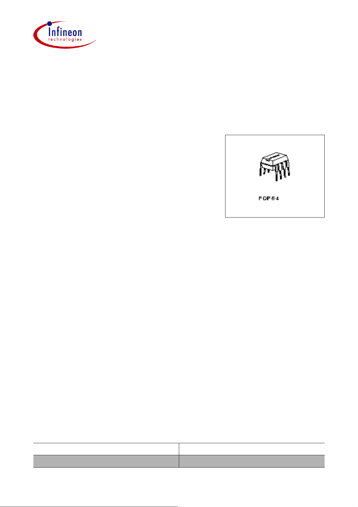
The device is available in a P-DIP-8-4 package.
The servo-loop-parameter pos.- and neg. Hysteresis, pos.- and neg. deadband and
angle-amplification are programmable with external resitors.
An internal window-comparator controls the input line. In the case of a fault condition,
like short circuit to GND, short circuit to supply-voltage, and broken wire, the
TLE 4209 stops the motor immediately (brake condition).
Furthermore the built in features like over- and undervoltage-lockout, short-circuitprotection and over-temperature-protection will open a wide range of automotive- and
industrial applications.
Type Package
TLE4209 P-DIP-8-4
Data Sheet 1 2000-09-05
TLE4209
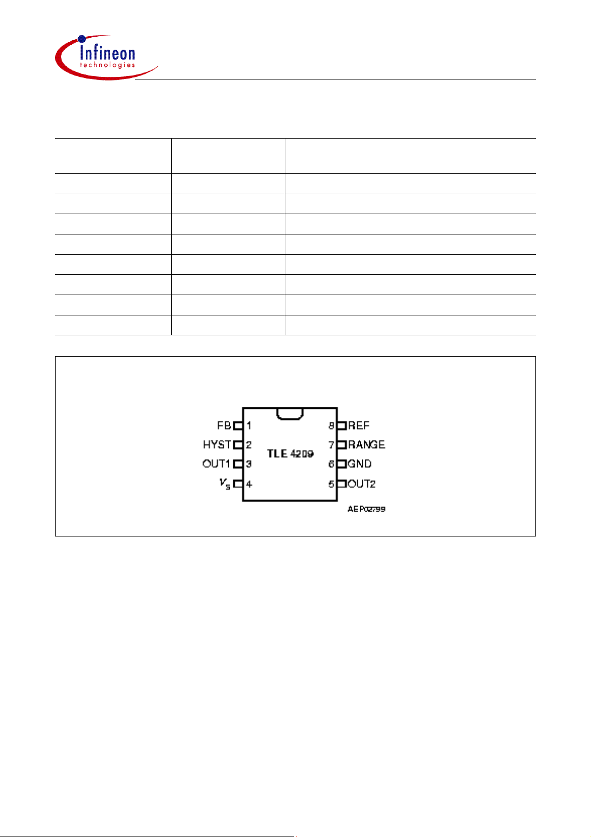
1.3 Pin Definitions and Functions
Pin No.
Symbol Function
P-DIP-8-4
1 FB Feedback Input
2 HYST Hysteresis I/O
3 OUT1 Power Output 1
4 V
S
Power Supply Voltage
5 OUT2 Power Output 2
6 GND Ground
7 RANGE Range Input
8 REF Reference Input
P-DIP-8-4
Overview
Figure1 Pin Configuration
(top view)
Data Sheet 2 2000-09-05
TLE4209
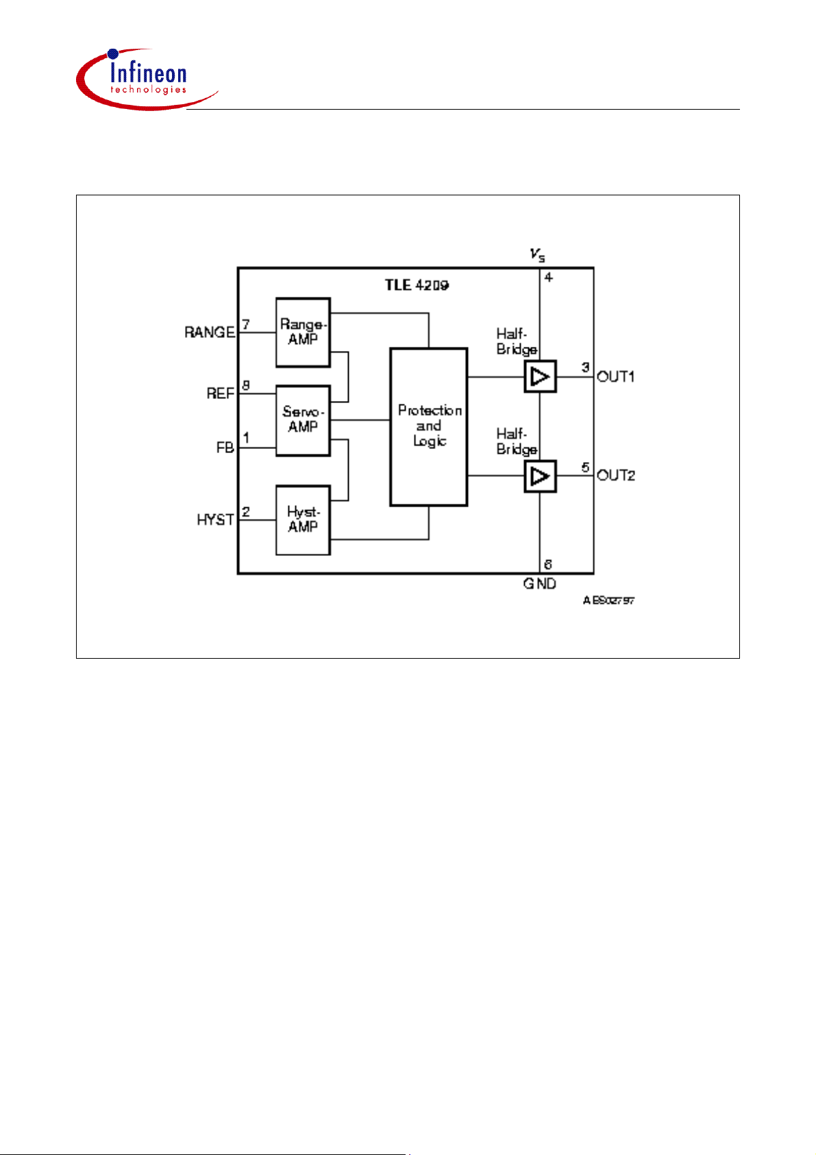
1.4 Functional Block Diagram
Overview
Figure 2 Block Diagram
Data Sheet 3 2000-09-05
TLE4209
1.5 Absolute Maximum Ratings
Parameter Symbol Limit Values Unit Remarks
min. max.
Voltages
Supply voltage V
Supply voltage V
Logic input voltages
V
S
S
I
– 0.3 45 V –
– 1 – V t < 0.5 s; IS > – 2 A
– 0.3 20 V –
(FB, REF, RANGE, HYST)
Currents
Output current (OUT1, OUT2) I
Output current (Diode) I
OUT
OUT
– – A internally limited
–1 1 A –
Overview
Input current
(FB, REF, RANGE, HYST)
I
IN
– 2
– 6
2
6
mA
mA t < 2 ms; t/T < 0.1
Temperatures
Junction temperature T
Storage temperature T
j
stg
– 40 150 °C –
– 50 150 °C –
Thermal Resistances
Junction ambient (P-DIP-8-4) R
thjA
100 K/W –
Note: Stresses above those listed here may cause permanent damage to the device.
Exposure to absolute maximum rating conditions for extended periods may affect
device reliability.
Data Sheet 4 2000-09-05

TLE4209
Overview
1.6 Operating Range
Parameter Symbol Limit Values Unit Remarks
min. max.
Supply voltage V
Supply voltage increasing V
Supply voltage decreasing V
Output current I
Input current (FB, REF) I
Junction temperature T
S
S
S
OUT1-2
IN
j
8 18 V After VS rising
– 0.3 V
– 0.3 V
F
UVON
UVOF
above V
V Outputs in tristate
V Outputs in tristate
UVON
– 0.8 0.8 A –
– 50 500 µA –
– 40 150 °C –
Note: In the operating range, the functions given in the circuit description are fulfilled.
1.7 Electrical Characteristics
8 V < VS < 18 V; I
OUT1-2
= 0 A; – 40 °C < Tj < 150 °C (unless otherwise specified)
Parameter Symbol Limit Values Unit Test Condition
min. typ. max.
Current Consumption
Supply current I
Supply current I
Supply current I
S
S
S
– 12 20 mA –
– 20 30 mA I
– 30 50 mA I
OUT1
I
OUT2
OUT1
I
OUT2
= 0.4 A
= – 0.4 A
= 0.8 A
= – 0.8 A
Over- and Under Voltage Lockout
UV Switch ON voltage V
UV Switch OFF voltage V
UVON
UVOFF
– 7.4 8 V VS increasing
6.3 6.9 – V VS decreasing
UV ON/OFF Hysteresis V
OV Switch OFF voltage V
OV Switch ON voltage V
OV ON/OFF Hysteresis V
Data Sheet 5 2000-09-05
UVHY
OVOFF
OVON
OVHY
– 0.5 – V V
UVON
– V
UVOFF
– 20.5 23 V VS increasing
17.5 20 – V VS decreasing
– 0.5 – V V
OVOFF
– V
OVON

TLE4209
Overview
1.7 Electrical Characteristics (cont’d)
8 V < VS < 18 V; I
OUT1-2
= 0 A; – 40 °C < Tj < 150 °C (unless otherwise specified)
Parameter Symbol Limit Values Unit Test Condition
min. typ. max.
Outputs OUT1-2
Saturation Voltages
Source (upper)
I
= –0.2A
OUT
Source (upper)
I
= –0.4A
OUT
Sink (upper)
I
= –0.8A
OUT
V
SATU
V
SATU
V
SATU
– 0.85 1.15 V Tj = 25 °C
– 0.90 1.20 V Tj = 25 °C
– 1.10 1.50 V Tj = 25 °C
Sink (lower)
I
= 0.2A
OUT
Sink (lower)
I
= 0.4A
OUT
Sink (lower)
I
= 0.8A
OUT
Total drop I
Total drop I
Total drop I
= 0.2 A V
OUT
= 0.4 A V
OUT
= 0.8 A V
OUT
V
V
V
Clamp Diodes
Forward voltage; upper V
SATL
SATL
SATL
SAT
SAT
SAT
FU
– 0.15 0.23 V Tj = 25 °C
– 0.25 0.40 V Tj = 25 °C
– 0.45 0.75 V Tj = 25 °C
– 1.0 1.4 V V
– 1.2 1.7 V V
– 1.6 2.5 V V
SAT
V
SAT L
SAT
V
SAT L
SAT
V
SAT L
= V
= V
= V
– 1.0 1.5 V IF = 0.4 A
SAT U
SAT U
SAT U
+
+
+
Upper leakage current I
Forward voltage; lower V
Data Sheet 6 2000-09-05
LKU
FL
– 5 mA IF = 0.4 A
– 0.9 1.4 V IF = 0.4 A

TLE4209
Overview
1.7 Electrical Characteristics (cont’d)
8 V < VS < 18 V; I
OUT1-2
= 0 A; – 40 °C < Tj < 150 °C (unless otherwise specified)
Parameter Symbol Limit Values Unit Test Condition
min. typ. max.
Input-Interface
Input REF
Quiescent voltage V
Input resistance R
REFq
REF
– 200 240 mV I
REF
= 0 µA
4.5 6.0 7.5 kΩ 0 V < V
REF
< 0.5 V
Input FB
Quiescent voltage V
FBq
– 200 240 mV IFB = 0 µA
Input resistance R
Input/Output HYST
Current Offset I
250
I
40
Current Amplification
A
HYST
= I
HYST
/ (I
REF
Current Gain
G
/ (I
HYST
REF
= (I
HYST
– IFB)
- I
HYSTIO40
– IFB)
A
G
)
FB
HYSTIO
HYSTIO
HYST
HYST
4.5 6.0 7.5 kΩ 0 V < V
–2 0.35 3 µA
IREF
FB
= IFB =
250 µA
–1.3 0 1.3 µA
V
IREF
HYST
= VS / 2
= IFB =
40 µA
V
HYST
= VS / 2
0.8 0.95 1.1 − –20 µA < I
< –10 µA;
10 µA < I
HYST
< 20 µA;
I
=250 µA
REF
0.8 0.95 1.1 - I
V
HYST
I
REF
V
= VS / 2
HYST
= +/-2µA;
=40 µA;
= VS / 2
HYST
< 0.5 V
HYST
Threshold voltage High V
V
Deadband voltage High V
V
Data Sheet 7 2000-09-05
HYH
S
DBH
S
/
51 52 54 % –
/
50 50.4 51 % –

TLE4209
Overview
1.7 Electrical Characteristics (cont’d)
8 V < VS < 18 V; I
OUT1-2
= 0 A; – 40 °C < Tj < 150 °C (unless otherwise specified)
Parameter Symbol Limit Values Unit Test Condition
min. typ. max.
Deadband voltage Low V
V
Threshold voltage Low V
V
Hysteresis Window V
Deadband Window V
V
DBL
S
HYL
S
HYW
V
S
DBW
S
/
49 49.6 50 % –
/
46 48 49 % –
/
3.0 4.0 5.0 % (V
/
0.4 0.8 1.2 % (V
HYH
DBH
– V
– V
HYL
DBL
)/ V
)/ V
Input RANGE
S
S
Input current I
Switch-OFF voltage High V
Switch-OFF voltage Low V
RANGE
OFFH
OFFL
– 1 – 1 µA 0V < V
< V
–25 0 100 mV refer to V
RANGE
S
S
300 400 500 mV refer to GND
Thermal Shutdown
Thermal shutdown junction
T
jSD
150 175 200 °C –
temperature
Thermal switch-on junction
T
jSO
120 – 170 °C –
temperature
Temperature hysteresis ∆T – 30 K –
Note: The listed characteristics are ensured over the operating range of the integrated
circuit. Typical characteristics specify mean values expected over the production
spread. If not otherwise specified, typical characteristics apply at TA = 25 °C and
the given supply voltage.
Data Sheet 8 2000-09-05

TLE4209
2 Diagrams
Diagrams
Figure 3 Application Circuit
Data Sheet 9 2000-09-05

TLE4209
Diagrams
Figure 4 Hysteresis, Phaselag and Deadband-Definitions
Data Sheet 10 2000-09-05

TLE4209
Diagrams
Figure 5 Timing and Phase-Lag
Data Sheet 11 2000-09-05

TLE4209
Sorts of Packing
Package outlines for tubes, trays etc. are contained in
our Data Book “Package Information”.
Dimensions in mm
3 Package Outlines
P-DIP-8-4
(Plastic Dual In-line Package)
Package Outlines
SMD = Surface Mounted Device
Data Sheet 12 2000-09-05
 Loading...