

Datasheet SPA06N80C3 Datasheet
SPA06N80C3
V
CoolMOSTM Power Transistor
Features
• New revolutionary high voltage technology
• Extreme dv/dt rated
• High peak current capability
• Qualified according to JEDEC
• Pb-free lead plating; RoHS compliant
• Ultra low gate charge
• Ultra low effective capacitances
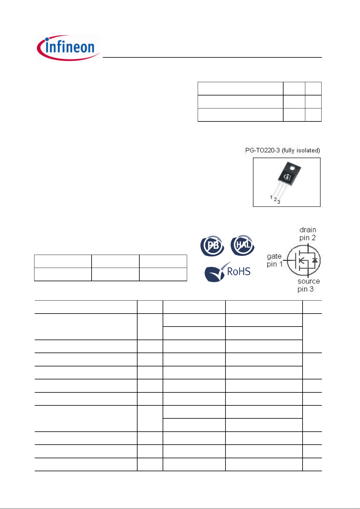
• Fully isolated package (2500 VAC; 1 minute)
CoolMOSTM 800V designed for:
• Industrial application with high DC bulk voltage
• Switching Application ( i.e. active clamp forward )
1)
for target applications
Product Summary
V
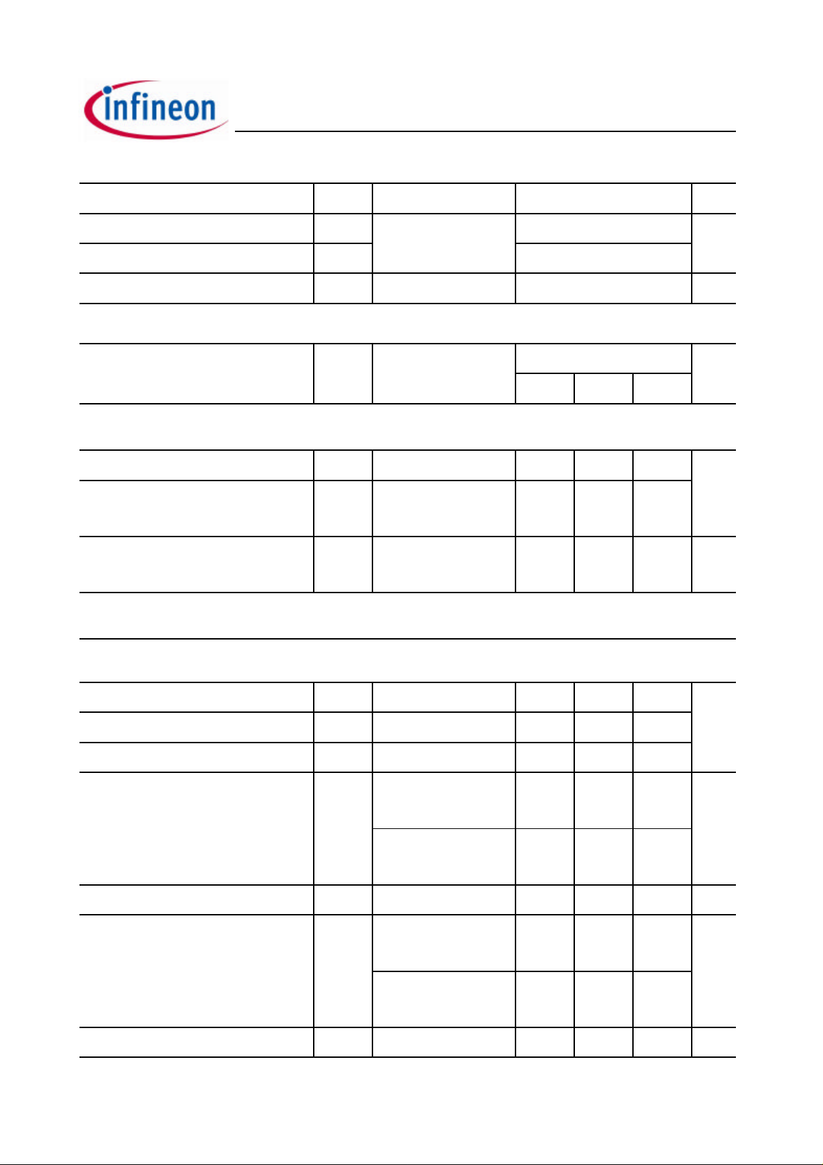
DS
R
DS(on)max @ Tj
Q
g,typ
= 25°C 0.9
800
Ω
31 nC
Type Package Marking
SPA06N80C3 PG-TO220-3 06N80C3
Maximum ratings, at Tj=25 °C, unless otherwise specified
Parameter Symbol Conditions Unit
Continuous drain current
2)
I
D
TC=25 °C
TC=100 °C
Pulsed drain current
3)
Avalanche energy, single pulse
Avalanche energy, repetitive t
Avalanche current, repetitive t
AR
AR
MOSFET dv/dt ruggedness dv/dt
Gate source voltage
3),4)
3),4)
I
D,pulse
E
AS
E
AR
I
AR
V
GS
TC=25 °C
ID=1.2 A, VDD=50 V
ID=6 A, VDD=50 V
VDS=0…640 V
static V
AC (f>1 Hz)
Value
6
3.8
18
230 mJ
0.2
6
50
±20
±30
A
A
V/ns
Power dissipation
Operating and storage temperature
P
tot
Tj, T
stg
TC=25 °C
39
-55 ... 150
W
°C
Mounting torque M2.5 screws 50 Ncm
Rev. 2.9
1 page 1 2011-09-27
Maximum ratings, at Tj=25 °C, unless otherwise specified
wave soldering only allowed at leads
SPA06N80C3
Parameter Symbol Conditions Unit
Continuous diode forward current
I
S
Value
6
A
TC=25 °C
Diode pulse current
Reverse diode dv/dt
3)
5)
Parameter Symbol Conditions Unit
I
S,pulse
dv/dt
18
4 V/ns
Values
min. typ. max.
Thermal characteristics
Thermal resistance, junction - case
Thermal resistance, junction -
ambient
Soldering temperature,
R
thJC
R
thJA
T
sold
leaded - - 80
1.6 mm (0.063 in.)
from case for 10s
- - 3.9 K/W
- - 260 °C
Electrical characteristics, at Tj=25 °C, unless otherwise specified
Static characteristics
Drain-source breakdown voltage
Avalanche breakdown voltage
Gate threshold voltage
Zero gate voltage drain current
V
(BR)DSSVGS
V
(BR)DSVGS
V
GS(th)
I
DSS
=0 V, ID=250 µA
=0 V, ID=6 A
VDS=VGS, ID=0.25 mA
VDS=800 V, VGS=0 V,
Tj=25 °C
VDS=800 V, VGS=0 V,
Tj=150 °C
Gate-source leakage current
Drain-source on-state resistance
I
R
GSS
DS(on)
VGS=20 V, VDS=0 V
VGS=10 V, ID=3.8 A,
Tj=25 °C
VGS=10 V, ID=3.8 A,
Tj=150 °C
800 - - V
- 870 -
2.1 3 3.9
- - 10 µA
- 50 -
- - 100 nA
- 0.78 0.9
- 2.1 -
Ω
Gate resistance
Rev. 2.9
1 page 2 2011-09-27
R
G
f=1 MHz, open drain
- 1.2 -
Ω
SPA06N80C3
Gate Charge Characteristics
Reverse Diode
=25 °C
Parameter Symbol Conditions Unit
Values
min. typ. max.
Dynamic characteristics
Input capacitance
Output capacitance
Effective output capacitance, energy
related
6)
Effective output capacitance, time
related
7)
Turn-on delay time
Rise time
C
C
C
C
t
t
iss
oss
o(er)
o(tr)
d(on)
r
VGS=0 V, VDS=100 V,
f=1 MHz
VGS=0 V, VDS=0 V
to 480 V
VDD=400 V,
- 785 - pF
- 33 -
- 26 -
- 69 -
- 25 - ns
- 15 -
VGS=0/10 V, ID=6 A,
Turn-off delay time
Fall time
t
t
d(off)
f
RG=15 ? , T
j
- 72 -
- 8 -
Gate to source charge
Gate to drain charge
Gate charge total
Gate plateau voltage
Diode forward voltage
Reverse recovery time
Reverse recovery charge
Peak reverse recovery current
1)
J-STD20 and JESD22
2)
Limited only by maximum temperature
3)
Pulse width tp limited by T
4)
Repetitive avalanche causes additional power losses that can be calculated as PAV=EAR*f.
5)
ISD=ID, di/dt=400A/µs, V
6)
C
is a fixed capacitance that gives the same stored energy as C
o(er)
7)
C
is a fixed capacitance that gives the same charging time as C
o(tr)
j,max
DClink
= 400V, V
Q
gs
Q
gd
Q
g
V
plateau
V
SD
t
rr
Q
rr
I
rrm
peak<V(BR)DSS
VDD=640 V, ID=6 A,
VGS=0 to 10 V
VGS=0 V, IF=IS=6 A,
Tj=25 °C
VR=400 V, IF=IS=6 A,
diF/dt=100 A/µs
, Tj<T
, identical low side and high side switch
jmax
while VDS is rising from 0 to 80% V
oss
while VDS is rising from 0 to 80% V
oss
- 4 - nC
- 15 -
- 31 41
- 5.5 - V
- 1 1.2 V
- 520 - ns
- 5 - µC
- 18 - A
DSS.
DSS.
Rev. 2.9
1 page 3 2011-09-27
 Loading...