

Page 1
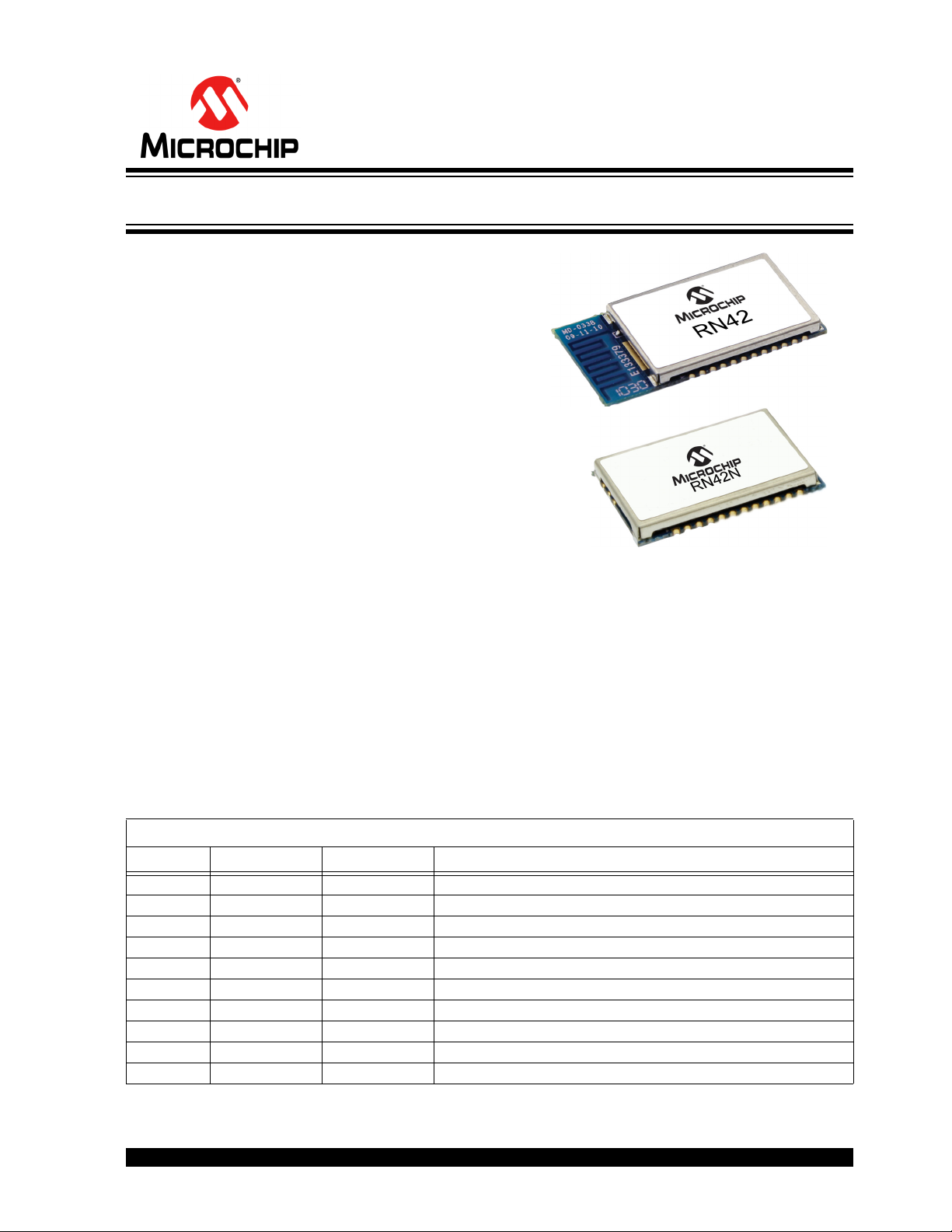
Class 2 Bluetooth® Module with EDR Support
Features
• Fully qualified Bluetooth® version 2.1 module, supports version 2.1 + Enhanced Data Rate (EDR)
• ASCII command interface over UART
• Postage-stamp-sized form factor:
- RN42: 13.4 x 25.8 x 2.4 mm
- RN42N: 13.4 x 20.5 x 2.4 mm
• Low-power (26 A sleep, 3 mA connected, 30 mA
transmit)
• UART (SPP or HCI) and USB (HCI only) data connection interfaces
• Sustained SPP data rates: 240 Kbps (Slave mode),
300 Kbps (Master mode)
• HCI data rates: 1.5 Mbps sustained, 3.0 Mbps burst
in HCI mode
• Embedded Bluetooth stack profiles include: GAP,
SDP, RFCOMM, L2CAP protocols, with SPP, HID,
and DUN profile support (does not require any host
stack).
• Bluetooth SIG qualified, end product listing
• Castellated SMT pads for easy and reliable PCB
mounting
• Class 2 power amplifier with on-board PCB trace
antenna (RN42) or external antenna (RN42N)
• Compliance (RN42)
- Modular Certified for the United States (FCC)
and Canada (IC)
- European R&TTE Directive Assessed Radio
Module
- Australia/New Zealand/Japan/Korea/Taiwan
- Bluetooth SIG QDID
• Integrated Crystal, Internal Voltage Regulator,
RN42/RN42N Module Variants
RN42/RN42N
Matching Circuitry, Power Amplifier, Low Noise,
Memory Amplifier and PCB Antenna
• Easy Integration into Final Product - Minimize Product Development, Quicker Time to Market
• Compatible with Microchip Microcontroller Families
(PIC16F, PIC18F, PIC24F/H, dsPIC33 and PIC32)
• Up to 10 meter range
Applications
• Cable replacement
• Barcode scanners
• Measurement and monitoring systems
• Industrial sensors and controls
• Medical devices
(1)
Model Antenna Firmware Description
RN42 Integral 4.77, 6.15 Class 2, 2.1+EDR, SPP profile
RN42HCI Integral N/A Class 2, 2.0+EDR, HCI over UART
RN42HID Integral 6.11 Class 2, 2.1+EDR, HID and SPP profiles
RN42U Integral N/A Class 2, 2.0+EDR, HCI over USB
RN42APL Integral 5.36, 5.43, 5.45 Class 2, 2.1+EDR, SPP & MFi profiles
RN42N External 4.77, 6.15 Class 2, 2.1+EDR, SPP profile
RN42NHCI External N/A Class 2, 2.0+EDR, HCI over UART
RN42NHID External 6.11 Class 2, 2.1+EDR, HID and SPP profiles
RN42NU External N/A Class 2, 2.0+EDR, HCI over USB
RN42NAPL External 5.36, 5.43, 5.45 Class 2, 2.1+EDR, SPP & MFi profiles
Note 1: For customer part numbers, see Section 4.0 “Ordering Information”. Information on firmware versions can be found
2015 Microchip Technology Inc. DS50002328A-page 1
on the RN42/RN42N product web page and the “Bluetooth Data Module Command Reference and Advanced Information
User’s Guide”.
Page 2

RN42/RN42N
Table of Contents
1.0 Device Overview ...........................................................................................................................................................................3
2.0 Application Information..................................................................................................................................................................7
3.0 Regulatory Approval....................................................................................................................................................................12
4.0 Ordering Information ...................................................................................................................................................................18
Appendix A: Revision History................................................................................................................................................................19
The Microchip Web Site........................................................................................................................................................................21
Customer Change Notification Service .................................................................................................................................................21
Customer Support.................................................................................................................................................................................21
Product Identification System ...............................................................................................................................................................23
TO OUR VALUED CUSTOMERS
It is our intention to provide our valued customers with the best documentation possible to ensure successful use of your Microchip
products. To this end, we will continue to improve our publications to better suit your needs. Our publications will be refined and
enhanced as new volumes and updates are introduced.
If you have any questions or comments regarding this publication, please contact the Marketing Communications Department via
E-mail at [email protected]. We welcome your feedback.
Most Current Data Sheet
To obtain the most up-to-date version of this data sheet, please register at our Worldwide Web site at:
http://www.microchip.com
You can determine the version of a data sheet by examining its literature number found on the bottom outside corner of any page.
The last character of the literature number is the version number, (e.g., DS30000000A is version A of document DS30000000).
Errata
An errata sheet, describing minor operational differences from the data sheet and recommended workarounds, may exist for current
devices. As device/documentation issues become known to us, we will publish an errata sheet. The errata will specify the revision
of silicon and revision of document to which it applies.
To determine if an errata sheet exists for a particular device, please check with one of the following:
• Microchip’s Worldwide Web site; http://www.microchip.com
• Your local Microchip sales office (see last page)
When contacting a sales office, please specify which device, revision of silicon and data sheet (include literature number) you are
using.
Customer Notification System
Register on our web site at www.microchip.com to receive the most current information on all of our products.
DS50002328A-page 2 2015 Microchip Technology Inc.
Page 3
RN42/RN42N
1.0 DEVICE OVERVIEW
The RN42/RN42N module is a small form factor, lowpower, class 2 Bluetooth radio that is ideal for
designers who want to add wireless capability to their
products without spending significant time and money
developing Bluetooth-specific hardware and software.
The RN42/RN42N supports multiple interface
protocols, is simple to design in, and is fully certified,
making it a complete embedded Bluetooth solution.
With its high-performance, PCB trace antenna (RN42)
or external antenna (RN42N), and support for
Bluetooth EDR, the RN42/RN42N delivers up to a 3Mbps data rate for distances up to 10 meters.
1.1 MCU Interface
The RN42/RN42N module is managed through ASCII
commands via the UART and/or PIO signals. A microcontroller unit (MCU) or host processor sends commands to configure module features, read status, and
manage Bluetooth data connections.
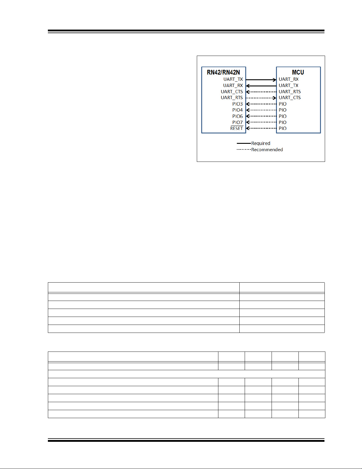
As shown in Figure 1-1, the UART TX and RX are
required to communicate with module, and transfer
data across Bluetooth SPP connection.
Connecting the hardware flow control lines CTS and
RTS is highly recommended for applications that
transmits a continuous stream of data.
The module can be configured locally via the UART or
over-the-air. To support instant cable replacement,
auto-discovery/pairing does not require software configuration. Additionally, the module supports auto-connect master, I/O pin (DTR), and character-based trigger
modes.
FIGURE 1-1: RN42/RN42N TO MCU
INTERFACE
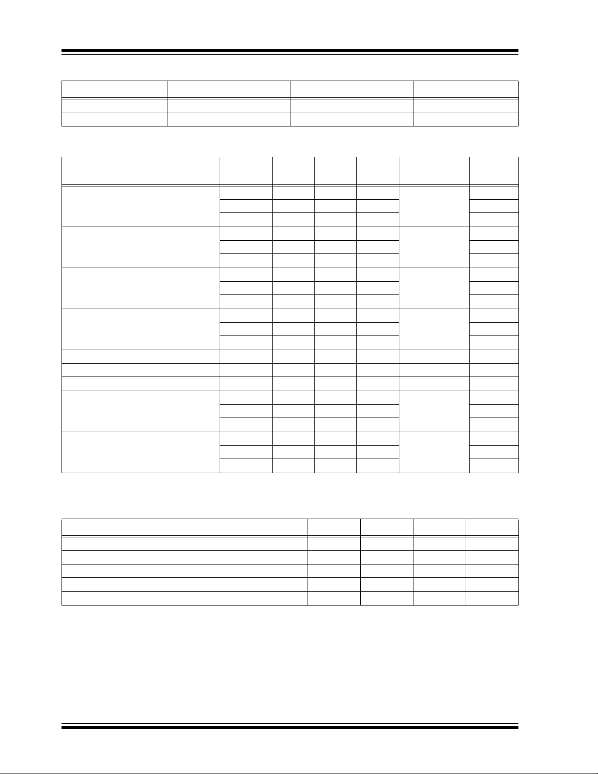
Table 1-1, Table 1-2, Ta bl e 1 -3 , Tab l e 1- 4, and Ta b le 1 5 provide the module’s environmental conditions, elec-
trical characteristics, dimensions, radio characteristics,
and digital I/O characteristics.
1.2 ASCII Command and Data
Interface
The “Bluetooth Data Module Advanced User’s Guide”
provides a complete description of the ASCII command
and data interface for the RN42/RN42N module.
TABLE 1-1: ENVIRONMENTAL CONDITIONS
Parameter Value
o
Temperature Range (Operating) -40
Temperature Range (Storage) -40
Relative Humidity (Operating) 90%
Relative Humidity (Storage) 90%
Moisture Sensitivity Level 1
C ~ 85o C
o
C ~ 85o C
TABLE 1-2: ELECTRICAL CHARACTERISTICS
Parameter Min. Typ. Max. Units
Supply Voltage (DC) 3.0 3.3 3.6 V
Average Power Consumption
Radio On (Discovery or Inquiry Window Time)
Connected Idle (No Sniff) — 25 — mA
Connected Idle (Sniff 100 ms) — 12 — mA
Connected with Data Transfer 40 45 50 mA
Deep Sleep Idle Mode — 26 — A
Note 1: This characteristic applies if, in Slave mode, there are bursts of radio on time that vary with the windows. The window setting
determines the average current.
2015 Microchip Technology Inc. DS50002328A-page 3
(1)
—40—mA
Page 4
RN42/RN42N
TABLE 1-3: MODULE DIMENSIONS
Parameter RN42 RN42N Units
Size
Weight
TABLE 1-4: RADIO CHARACTERISTICS
Parameter
Sensitivity at 0.1% BER 2.402 — -80 -86 ≤ -70 dBm
RF Transmit Power
RN42
RF Transmit Power
RN42N
Initial Carrier Frequency Tolerance 2.402 — 5 75 75 kHz
20-dB Bandwidth for Modulated Carrier — — 900 1000 ≤ 1000 kHz
Drift (Five Slots Packet) — — 15 — 40 kHz
Drift Rate — — 13 — 20 kHz
∆f1
Maximum Modulation 2.402 140 165 175 > 140 kHz
avg
∆f2
Minimum Modulation 2.402 140 190 — 115 kHz
avg
Note 1: Normal mode
(1)
(1)
13.4 x 25.8 x 2.4 13.4 x 20.5 x 2.4
0.045 0.040
Frequency
(GHz)
2.441 — -80 -86 dBm
2.480 — -80 -86 dBm
2.402 — 4 — dBm
2.441 — 4 — dBm
2.480 — 4 — dBm
2.402 — 4 — dBm
2.441 — 4 — dBm
2.480 — 4 — dBm
2.441 — 5 75 kHz
2.480 — 5 75 kHz
2.441 140 165 175 kHz
2.480 140 165 175 kHz
2.441 140 190 — kHz
2.480 140 190 — kHz
Min. Typ. Max.
mm
oz.
Bluetooth
Specification
Units
TABLE 1-5: DIGITAL I/O CHARACTERISTICS
3.0 V ≤ VDD ≤ 3.3 V Min. Typ. Max. Units
Input Logic Level Low -0.4 — +0.8 V
Input Logic Level High 0.7 VDD — VDD + 0.4 V
Output Logic Level Low — — 0.2 V
Output Logic Level High VDD - 0.2 — — V
All I/O pins (Except reset) Default to Weak Pull Down +0.2 +1.0 +5.0 A
DS50002328A-page 4 2015 Microchip Technology Inc.
Page 5
RN42/RN42N
0.80mm
0.0
2.6
1.1
3.6
4.9
6.1
7.3
8.5
9.8
10.8
12.3
13.4
0.0
0.7
2.8
4.0
5.2
6.4
7.6
8.8
10.0
11.2
12.4
13.6
14.8
16.0
25.8
19.7
20.5
PCB Outline: +/- 0.13 mm
PCB Thickness: +/- 0.1 mm
Tolerances:
Top View Side View
Dimensions are in millimeters
0.0
0.8
2.4
0.0
25.8
0.80mm
0.0
2.6
1.1
3.6
4.9
6.1
7.3
8.5
9.8
10.8
12.3
13.4
0.0
0.7
2.8
4.0
5.2
6.4
7.6
8.8
10.0
11.2
12.4
13.6
14.8
16.0
19.7
20.5
PCB Outline: +/- 0.13 mm
PCB Thickness: +/- 0.1 mm
Tolerances:
Top View
Dimensions are in millimeters
0.0
0.8
2.4
0.0
20.5
Side View
8.9
10.5
7.3
GND
SPI_MOSI
GPIO6
GPIO7
RESET
PCM_CLK
PCM_IN
PCM_OUT
VDD
GND
SPI_MISO
SPI_CSB
GPIO4
GPIO5
GPIO3
GPIO2
USB_DUSB_D+
UART_TX
UART_RX
1
2
3
4
5
6
7
8
9
10
11
12
24
23
22
21
20
19
18
17
16
15
14
13
AIO1
GND
GPIO9
GPIO8
GND
AIO0
35 29 34 33 32 31 28 30
RN42
Top View
GND
SPI_MOSI
GPIO6
GPIO7
RESET
SPI_CLOCK
PCM_CLK
PCM_SYNC
PCM_IN
PCM_OUT
VDD
GND
SPI_MISO
SPI_CSB
GPIO4
GPIO5
GPIO3
GPIO2
USB_D-
USB_D+
UART_CTS
UART_RTS
UART_TX
UART_RX
1
2
3
4
5
6
7
8
9
10
11
12
24
23
22
21
20
19
18
17
16
15
14
13
AIO1
GND
GPIO11
GPIO9
GPIO8
GND
AIO0
35 29 34 33 32 31 28 30
RN42N
Top View
GND
RFPAD
GND
27 26 25
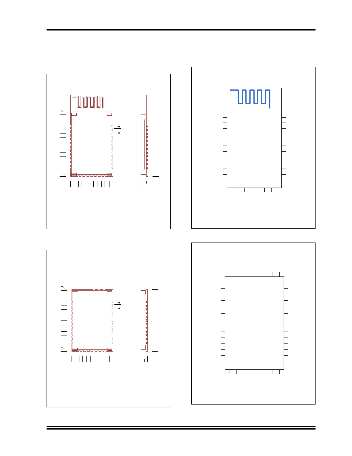
Figure 1-2 and Figure 1-3 show the modules’
dimensions.
FIGURE 1-2: RN42 MODULE
DIMENSIONS
Figure 1-4 and Figure 1-5 show the pinout and
Table 1-6 describes the module’s pins.
FIGURE 1-4: RN42 PIN DIAGRAM
SPI_CLOCK
PCM_SYNC
UART_CTS
UART_RTS
GPIO11
GPIO10
FIGURE 1-3: RN42N MODULE
2015 Microchip Technology Inc. DS50002328A-page 5
DIMENSIONS
FIGURE 1-5: RN42N PIN DIAGRAM
Page 6
RN42/RN42N
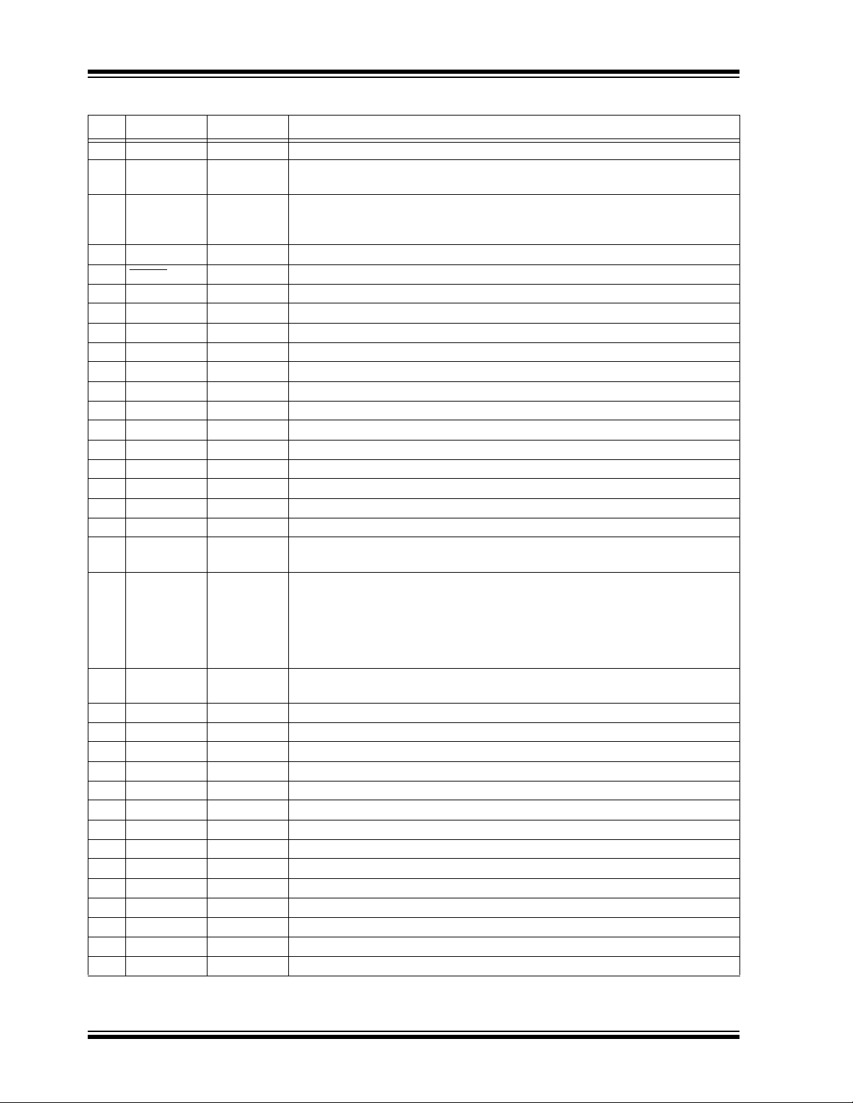
TABLE 1-6: PIN DESCRIPTION
Pin Symbol Type Description
1 GND Power Ground reference
2 SPI_MOSI DI (Optional) Factory diagnostic, programming and test. See Section 2.8 “SPI
Interface”.
3 GPIO6 DI Set Bluetooth master.
If GPIO6 = high, module connects to the stored address.
If GPIO3 = high, module enters new Discovery/Pairing mode.
4 GPIO7 DIO Set baud rate (high = force 9,600, low = 115K or firmware setting)
5 RESET
6 SPI_CLK DI (Optional) Factory diagnostic and test. See Section 2.8 “SPI Interface”.
7 PCM_CLK DIO (Do not connect) PCM interface
8 PCM_SYNC DIO (Do not connect) PCM interface
9 PCM_IN DI (Do not connect) PCM interface
10 PCM_OUT DO (Do not connect) PCM interface
11 VDD Power Positive Supply
12 GND Power Ground reference
13 UART_RX DI UART receive input
14 UART_TX DO UART transmit output
15 UART_RTS DO UART RTS, goes high to disable host transmitter
16 UART_CTS DI UART CTS, if set high, it disables transmitter
17 USB_D+ DIO USB port. 1.5K pullup activated when USB port is ready (~500 ms after reset).
18 USB_D- DIO USB port
19 GPIO2 DIO Status, high when connected, low otherwise. See Section 2.3 “Connection
20 GPIO3 DI Auto-discovery mode = high.
21 GPIO5 DIO Status, toggles based on state, low on connect. See Section 2.3 “Connection
22 GPIO4 DIO Set factory defaults. See Section 2.2 “Factory Reset Using GPIO4”.
23 SPI_CSB DI (Optional) Factory diagnostic and test. See Section 2.8 “SPI Interface”.
24 SPI_MISO DO (Optional) Factory diagnostic and test. See Section 2.8 “SPI Interface”.
25 GND Power Ground reference (RN42N only)
26 RF ANT AIO Antenna, 50-Ohm impedance (RN42N only)
27 GND Power Ground reference (RN42N only)
28 GND Power Ground reference
29 GND Power Ground reference
30 AIO0 AIO (Not used) Optional analog input
31 GPIO8 DO UART TX/RX data activity
32 GPIO9 DIO I/O
33 GPIO10 DIO I/O (remote DTR signal)
34 GPIO11 DIO I/O (remote RTS signal)
35 AIO1 AIO (Not used) Optional analog input
Pin type abbreviation: A = Analog, D = Digital, I = Input, O = Output.
Note 1: Pin numbers 7 through 10 are reserved for future use.
DI Active-low Reset
(1)
(1)
(1)
(1)
Status”.
If GPIO6 = high, module performs device enquiry scan searching for a device
with matching class of 0x55AA. If a device is found, the address of the device is
stored in the remote address field and auto-connects.
If GPIO6 = low, module enters Slave mode with special matching class of
0x55AA and waits for a master to discover it.
Status”.
DS50002328A-page 6 2015 Microchip Technology Inc.
Page 7
RN42/RN42N
0.70mm
0.80mm
2.00mm
0.0
2.6
1.1
3.6
4.9
6.1
7.3
8.5
9.8
10.8
12.3
13.4
0.0
0.7
2.8
4.0
5.2
6.4
7.6
8.8
10.0
11.2
12.4
13.6
14.8
16.0
25.8
19.7
Shield Pads
4 Corners
1.0 x 1.8mm
20.5
Do not locate
vias or surface
traces under
Shield Pads
Top View
Dimensions are in millimeters
2.0 APPLICATION INFORMATION
The following sections provide information on designing with the RN42/RN42N module, including radio
interference, factory reset, solder reflow profile, connection status, and so on.
2.1 Reset Circuit
The RN42/RN42N contains a weak internal pull-up to
VCC, and the reset polarity is active low. The module’s
reset pin has an optional Power-on Reset circuit with a
delay, which should only be required if the input power
supply has a very slow ramp or tends to bounce or have
instability on power-up. Often a microcontroller or
embedded CPU I/O is available to generate the reset
once power is stable. If not, designers can use one of
the many low-cost power supervisor chips available,
such as the MCP809 or MCP102/121.
2.2 Factory Reset Using GPIO4
It is recommended to connect the GPIO4 pin to a
switch, jumper, or resistor so it can be accessed. This
pin can be used to reset the module to its factory
default settings, which is critical in situations where the
module has been misconfigure d. To reset the module
to the factory defaults, GPIO4 should be high on
power-up and then toggle between low and high twice
with a 1 second wait between the low-high transitions.
2.4 Module Mounting Details
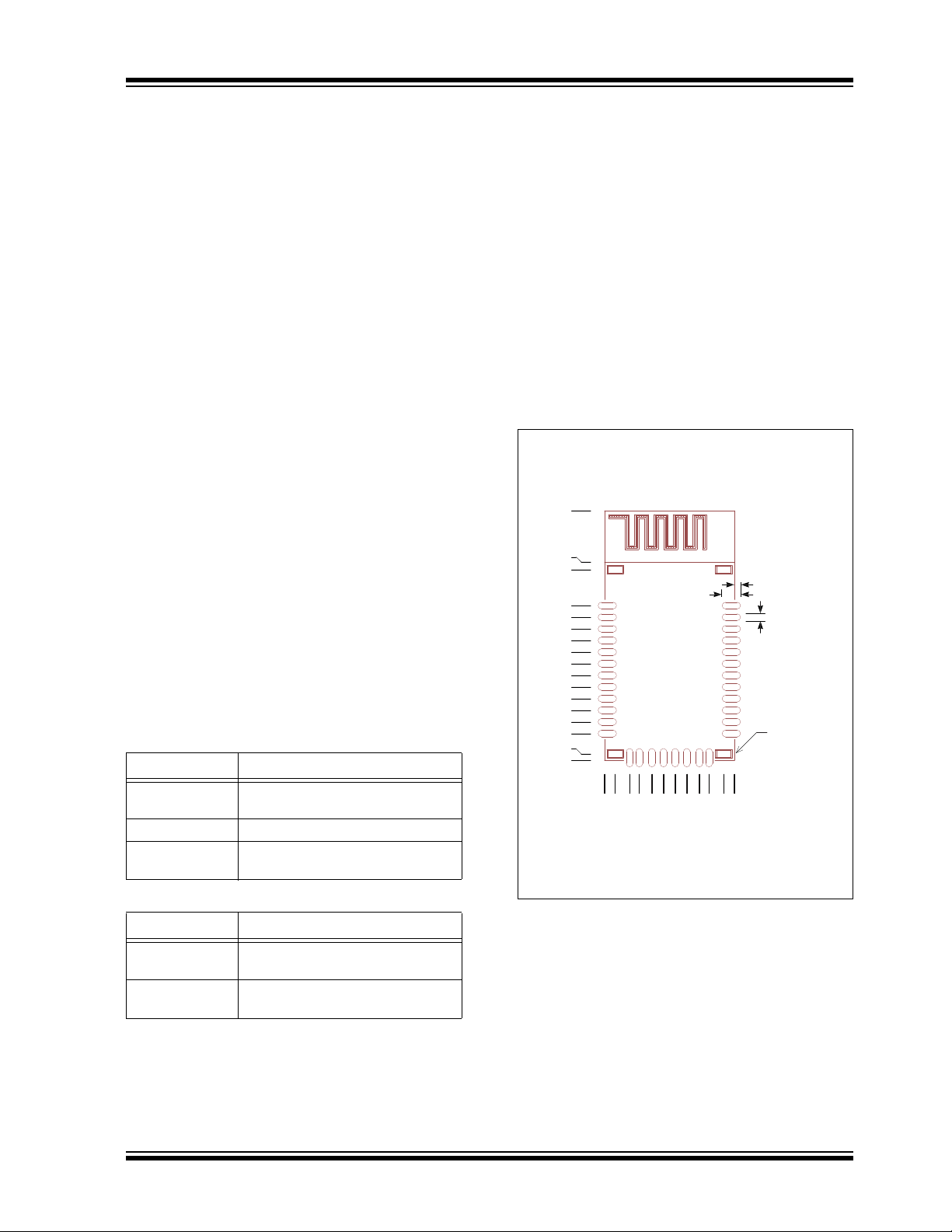
Figure 2-1 and Figure 2-2 show the recommended
PCB footprint for the RN42 and RN42N, respectively.
When laying out the carrier board for the RN42 module,
the areas under the antenna and shielding connections
should not have surface traces, ground planes, or
exposed vias.
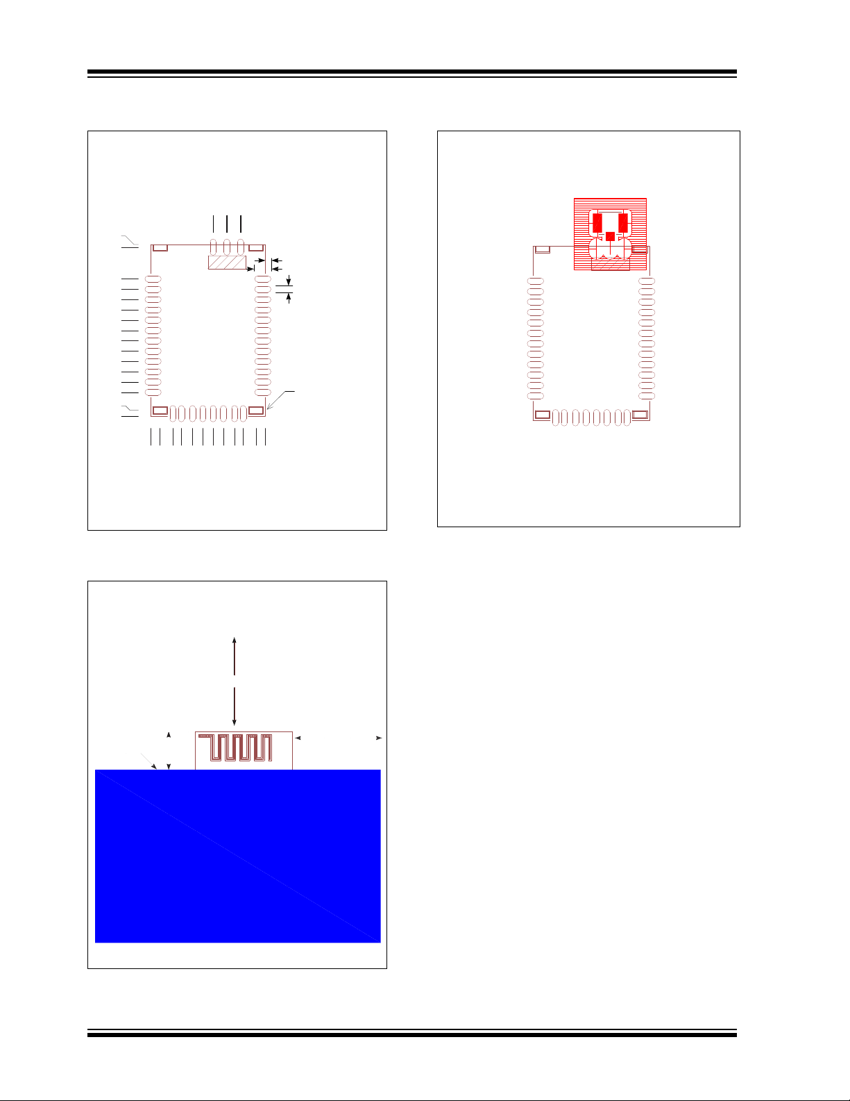
Figure 2-3 and Figure 2-4 show the recommended
mounting details for the RN42 and RN42N, respectively. For optimal radio performance, the RN42 module’s antenna end should protrude at least 31 mm
beyond any metal enclosure.
Figure 2-5 shows examples of good, bad, and accept-
able positioning of the RN42/RN42N on the host PCB.
FIGURE 2-1: RN42 RECOMMENDED
PCB FOOTPRINT
2.3 Connection Status
GPIO5 is available to drive an LED, and it blinks at various speeds to indicate status, see Table 2-1. GPIO2 is
an output that directly reflects the connection state as
shown in Ta b le 2 - 2 .
TABLE 2-1: GPIO5 STATUS
GPIO5 Status Description
Toggle at 1 Hz The module is discoverable and
waiting for a connection.
Toggle at 10 Hz The module is in command mode.
High The module is connected to
another device over Bluetooth.
TABLE 2-2: GPIO2 STATUS
GPIO2 Status Description
High The module is connected to
Low The module is not connected over
2015 Microchip Technology Inc. DS50002328A-page 7
another device over Bluetooth.
Bluetooth.
Page 8
RN42/RN42N
0.70mm
0.80mm
2.00mm
0.0
2.6
1.1
3.6
4.9
6.1
7.3
8.5
9.8
10.8
12.3
13.4
0.0
0.7
2.8
4.0
5.2
6.4
7.6
8.8
10.0
11.2
12.4
13.6
14.8
16.0
19.7
Shield Pads
4 Corners
1.0 x 1.8mm
20.0
Do not locate vias
or surface traces
under Shield Pads
Top View
Dimensions are in millimeters
8.9
10.5
7.3
20.5mm
5.3mm
Top View
Keep area around antenna
(approximately 31 mm) clear
of metallic structures for
best performance
31mm
Edge of
Ground
Plane
31cm
Note: Example U.FL connector layout
Top View
FIGURE 2-2: RN42N RECOMMENDED
PCB FOOTPRINT
FIGURE 2-4: RN42N MODULE
MOUNTING DETAILS
FIGURE 2-3: RN42 MODULE
DS50002328A-page 8 2015 Microchip Technology Inc.
MOUNTING DETAILS
Page 9
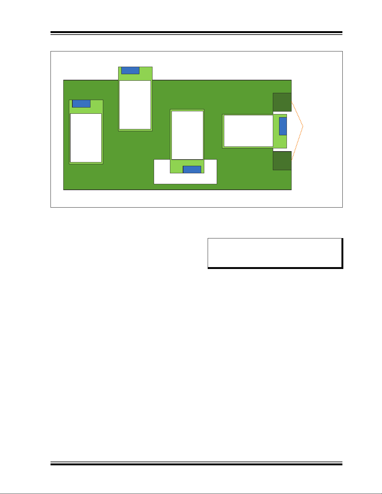
FIGURE 2-5: RN42 HOST PCB EXAMPLE LAYOUT
No Copper
in these
areas
RN42
Okay
RN42
Best
RN42
Okay
RN42
Okay
RN42/RN42N
2.5 External Antenna Types (RN42N)
The RN42N module’s antenna pin (pin 26) provides a
50-ohm impedance to external antennas. Pin 25 can
connect directly to a coaxial cable or to an antenna
connector such as a U.FL or reverse polarity SMA.
The PCB trace from pin 26 to the coaxial cable or connector should be less than 0.2 inches (5 mm) for minimum loss and the best impedance match. If the PCB
trace is longer, it should be a 50-ohm impedance
microstrip trace. Connect adjacent ground pins 25 and
27 to a low-impedance ground on the host PCB and the
antenna connection. Figure 2-4 gives example host
PCB layout to a U.FL connector.
2.6 HCI Mode
Microchip offers the Host Controller Interface (HCI)
mode in addition to the standard operational mode of its
Bluetooth modules (standard mode refers to the onboard stack running on the module).
In HCI mode, the on-board stack is bypassed and the
module is put in a state that runs the Bluetooth baseband. The HCI provides a command reference interface to the baseband controller and the link manager,
and provides access to the hardware status and control
registers. This interface provides a uniform method for
accessing the Bluetooth baseband capabilities.
In this mode, the Bluetooth stack is no longer on-board
the module. It is offloaded to the interfacing host processor. The Bluetooth module is used as a radio, performing the lower level MAC functionalities, while the
application stack runs on the host processor.
Using the module in HCI mode enables designers to
implement profiles that are not natively supported on
the Bluetooth module.
Note: HCI mode is only available by ordering
part RN42HCI and RN42HCI for UART
interface; or RN42U and RN42U for USB
interface.
Microchip offers HCI mode in two hardware interfaces:
• HCI over UART (RN42HCI-I/RM)
• HCI over USB (RN42U-I/RM)
2.6.1 HCI OVER UART
In this mode, the hardware interface between the host
processor and the Bluetooth module is the UART configured at 115.2Kbps. The UART hardware flow control
signals are required between the host processor and
the Bluetooth module for the HCI interface to work.
Failure to do so can cause the host processor and the
Bluetooth module to become out of sync and break the
Bluetooth link.
2.6.2 HCI OVER USB
In this mode, the hardware interface between the host
processor and the Bluetooth module is the USB. In this
architecture, the Bluetooth module is the USB slave
and the host processor is the USB host.
Using the USB interface offers the advantage of a
faster data link between the Bluetooth module and the
host processor. With this interface, it is possible to
achieve Bluetooth’s theoretical maximum throughput of
3 Mpbs.
2015 Microchip Technology Inc. DS50002328A-page 9
Page 10
RN42/RN42N
2.7 Soldering Recommendations
The RN42/RN42N wireless module was assembled
using standard lead-free reflow profile IPC/JEDEC JSTD-020.
The module can be soldered to the host PCB using
standard leaded and lead-free solder reflow profiles.
To avoid damaging the module, the following recommendations are given:
• Microchip Technology Application Note,” AN233
Solder Reflow Recommendation” (DS00233) provides solder reflow recommendations
• Do not exceed peak temperature (T
• Refer to the Solder Paste data sheet for specific
reflow profile recommendations
• Use no-clean flux solder paste
• Do not wash as moisture can be trapped under
the shield
• Use only one flow. If the PCB requires multiple
flows, apply the module on the final flow.
2.8 SPI Interface
) of 250 C°
p
The SPI Interface is primarily used for factory programming, test, and diagnostics. Although not required, the
SPI interface is useful for restoring a corrupted flash
image or enabling test modes required for certification
testing.
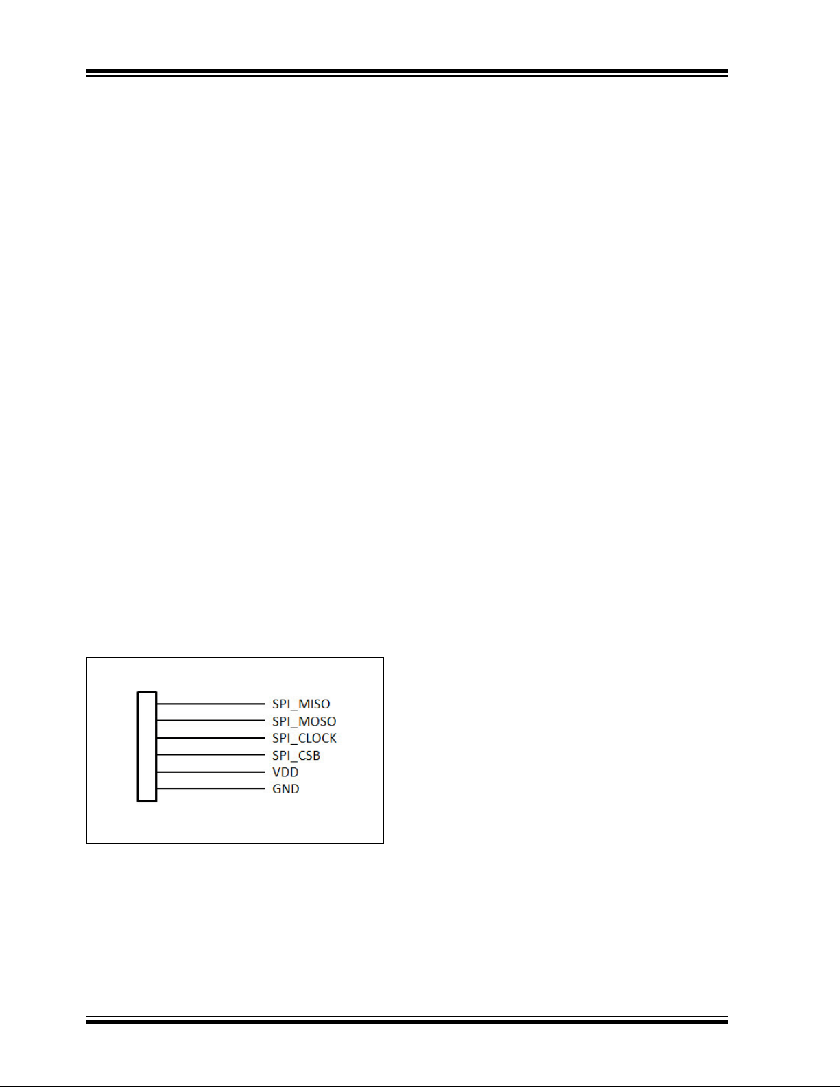
When module is installed in a final product that requires
European type approval, see Section 3.3 “Europe”, it
is recommended that the SPI interface should be
accessible via 6-pin header as shown in Figure 2-6.
FIGURE 2-6: OPTIONAL SPI
INTERFACE
2.9 Bluetooth SIG QDID
The RN42 has a QDID registered with the Bluetooth
SIG. The manufacturer using the RN42 module in their
end product can reference this QDID when filing an
EPL (end product listing) to use Bluetooth
logo. For more information, please visit the Bluetooth
SIG at www.bluetooth.org.
QDID: B014867
DS50002328A-page 10 2015 Microchip Technology Inc.
®
brand and
Page 11
TXD
RX D
GND
1
SPI _MOSI
2
PIO 6
3
PIO 7
4
RESET
5
SPI _SCK
6
PCM_CL K
7
PCM_SYNC
8
PCM_I N
9
PCM_OUT
10
VDD
11
GND
12
UART_RX
13
UART_TX
14
UART_RTS
15
UART_CTS
16
USB_D+
17
USB_D-
18
PIO 2
19
PIO 3
20
PIO 5
21
PIO 4
22
SPI _CS#
23
SPI _MI SO
24
GND
2
8
GND
29
A
IO0
3
0
PI
O8
31
PI
O9
3
2
PI
O10
33
PIO1
1
34
AIO135SH
IELD
0
M1 RN42 Module
SPI _MI SO
SPI _MOSI
SPI _SCK
SPI _SS
RT S
CT S
RESET _N
PIO 6
PIO 7
PIO 4
PIO 5
PIO 3
PIO 2
AIO1
AI
O0
PIO11
PIO10
PIO9PIO8
1
2
3
4
5
6
J3
SPI MASTER
SPI _MI SO
SPI _MOSI
SPI _SCK
SPI _SS
3.3V
3.3V
PCM_CL K
PCM_SYNC
PCM_OUT
PCM_I N
100k
R17
300k
R18
100k
R16
300k
R15
V
B
1
V
B2
A
IO0
A
IO1
1
2
3
4
5
6
7
8
9
10
11
12
J1
HEADER 1
1
2
3
4
5
6
7
8
9
10
11
12
J2
HEADER 2
PIO 6
PIO 7
RESET _N
RX D
TX D
RT S
CT S
PIO 4
PIO 3
PIO 2
PIO11
PIO10
PIO 9
PIO 8
3.3V
VB1
VB2
SHDN
D_N
D_P
TXD
RXD
RTS
CTS
VBUS
RESET
18
3V 3OUT
16
USBDP
14
USBDM
15
GND
1
7
CBUS2
10
CBUS1
21
VC
CI
O
1
CBUS3
11
CBUS4
9
CBUS0
22
GND
20
RI
3
DCD
7
DSR
6
DTR
31
CTS
8
RTS
32
RXD
2
TXD
30
VCC
19
OSCI
27
OSCO
28
AGND24TEST
2
6
GND4THPAD
33
FT232RQ
U3
100nF
C6
100nF
C5
100nF
C4
GND
5
D+
3
D-
2
VBUS
1
MTAB
6
USB Mini B
J4
3k3R12
3k3
R13
3k3
R11
3k3
R14
VBUS
3.3V VBUS
VI N
1
G
ND
2
SHDN
3
BYP
4
VOUT
5
U1 TC1185
1uF
C2
1uF
C1
SHDN
3k3
R1
1
2
3
4
S1
3k3R10
3k3
R9
3k3
R8
3k3
R7
3.3V
PIO 4
PIO 3
PIO 6
PIO 7
Red LEDD2
Activity
PIO 5
3.3V
PIO 8
Green LED
D1
Connection Status
470
R2
470
R3
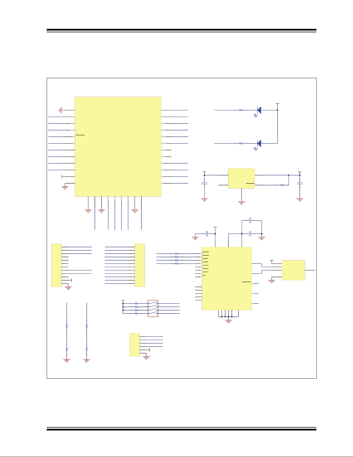
2.10 Application Schematic
Figure 2-7 shows an example application circuit. This schematic is for the RN-42-EK development tool. For details on
how to connect RN42/RN42N to a microcontroller, see Section 1.1 “MCU Interface”.
FIGURE 2-7: EXAMPLE APPLICATION CIRCUIT
RN42/RN42N
2015 Microchip Technology Inc. DS50002328A-page 11
Page 12

RN42/RN42N
3.0 REGULATORY APPROVAL
This section outlines the regulatory information for the
RN42 module for the following countries:
• United States
• Canada
• Europe
• Australia
• New Zealand
• Japan
• Korea
• Taiwan
3.1 United States
The RN42 module has received Federal Communications Commission (FCC) CFR47 Telecommunications,
Part 15 Subpart C “Intentional Radiators” modular
approval in accordance with Part 15.212 Modular
Transmitter approval. Modular approval allows the end
user to integrate the RN42 module into a finished product without obtaining subsequent and separate FCC
approvals for intentional radiation, provided no
changes or modifications are made to the module circuitry. Changes or modifications could void the user’s
authority to operate the equipment. The end user must
comply with all of the instructions provided by the
Grantee, which indicate installation and/or operating
conditions necessary for compliance.
The finished product is required to comply with all applicable FCC equipment authorizations regulations,
requirements and equipment functions not associated
with the transmitter module portion. For example, compliance must be demonstrated to regulations for other
transmitter components within the host product; to
requirements for unintentional radiators (Part 15 Subpart B “Unintentional Radiators”), such as digital
devices, computer peripherals, radio receivers, etc.;
and to additional authorization requirements for the
non-transmitter functions on the transmitter module
(i.e., Verification, or Declaration of Conformity) (e.g.,
transmitter modules may also contain digital logic functions) as appropriate.
3.1.1 LABELING AND USER
INFORMATION REQUIREMENTS
The RN42 module has been labeled with its own FCC
ID number, and if the FCC ID is not visible when the
module is installed inside another device, then the outside of the finished product into which the module is
installed must also display a label referring to the
enclosed module. This exterior label can use wording
as follows:
Contains Transmitter Module FCC ID: T9J-RN42
or
Contains FCC ID: T9J-RN42
This device complies with Part 15 of the FCC Rules.
Operation is subject to the following two conditions:
(1) this device may not cause harmful interference,
and (2) this device must accept any interference
received, including interference that may cause
undesired operation.
A user’s manual for the product should include the following statement:
This equipment has been tested and found to comply
with the limits for a Class B digital device, pursuant to
part 15 of the FCC Rules. These limits are designed
to provide reasonable protection against harmful
interference in a residential installation. This equipment generates, uses and can radiate radio frequency energy, and if not installed and used in
accordance with the instructions, may cause harmful
interference to radio communications. However,
there is no guarantee that interference will not occur
in a particular installation. If this equipment does
cause harmful interference to radio or television
reception, which can be determined by turning the
equipment off and on, the user is encouraged to try to
correct the interference by one or more of the following measures:
• Reorient or relocate the receiving antenna.
• Increase the separation between the equipment
and receiver.
• Connect the equipment into an outlet on a circuit
different from that to which the receiver is connected.
• Consult the dealer or an experienced radio/TV
technician for help.
Additional information on labeling and user information
requirements for Part 15 devices can be found in KDB
Publication 784748 available at the FCC Office of Engineering and Technology (OET) Laboratory Division
Knowledge Database (KDB) http://apps.fcc.gov/oetcf/
kdb/index.cfm.
DS50002328A-page 12 2015 Microchip Technology Inc.
Page 13

RN42/RN42N
3.1.2 RF EXPOSURE
All transmitters regulated by FCC must comply with RF
exposure requirements. KDB 447498 General RF
Exposure Guidance provides guidance in determining
whether proposed or existing transmitting facilities,
operations or devices comply with limits for human
exposure to Radio Frequency (RF) fields adopted by
the Federal Communications Commission (FCC).
From the FCC Grant: Power Output listed is conducted.
This module must be installed by the OEM or OEM integrator. Instructions on installation of this module may
not be provided to the end user. The antenna used for
this transmitter must not be co-located with any other
transmitters except in accordance with FCC multitransmitter product. procedures. Installers must be provided with antenna installation instructions for satisfying RF exposure compliance. Installers and end users
must be provided with transmitter operating conditions
for satisfying RF exposure compliance.
3.1.3 HELPFUL WEB SITES
Federal Communications Commission (FCC): http://
www.fcc.gov
FCC Office of Engineering and Technology (OET) Laboratory Division Knowledge Database (KDB): http://
apps.fcc.gov/oetcf/kdb/index.cfm
3.2 Canada
The RN42 module has been certified for use in Canada
under Industry Canada (IC) Radio Standards Specification (RSS) RSS-210 and RSSGen. Modular approval
permits the installation of a module in a host device
without the need to recertify the device.
3.2.1 LABELING AND USER
INFORMATION REQUIREMENTS
Labeling Requirements for the Host Device (from Section 3.2.1, RSS-Gen, Issue 3, December 2010): The
host device shall be properly labeled to identify the
module within the host device.
The Industry Canada certification label of a module
shall be clearly visible at all times when installed in the
host device, otherwise the host device must be labeled
to display the Industry Canada certification number of
the module, preceded by the words “Contains transmitter module”, or the word “Contains”, or similar wording
expressing the same meaning, as follows:
RN42:
Contains transmitter module IC: 6514A-RN42
User Manual Notice for License-Exempt Radio Apparatus (from Section 7.1.3 RSS-Gen, Issue 3, December
2010): User manuals for license-exempt radio apparatus shall contain the following or equivalent notice in a
conspicuous location in the user manual or alternatively on the device or both:
This device complies with Industry Canada licenseexempt RSS standard(s). Operation is subject to the
following two conditions: (1) this device may not
cause interference, and (2) this device must accept
any interference, including interference that may
cause undesired operation of the device.
Le présent appareil est conforme aux CNR d'Industrie Canada applicables aux appareils radio exempts
de licence. L'exploitation est autorisée aux deux conditions suivantes: (1) l'appareil ne doit pas produire
de brouillage, et (2) l'utilisateur de l'appareil doit
accepter tout brouillage radioélectrique subi, même
si le brouillage est susceptible d'en compromettre le
fonctionnement.
Transmitter Antenna (from Section 7.1.2 RSS-Gen,
Issue 3, December 2010): User manuals for transmitters shall display the following notice in a conspicuous
location:
Under Industry Canada regulations, this radio transmitter may only operate using an antenna of a type
and maximum (or lesser) gain approved for the transmitter by Industry Canada. To reduce potential radio
interference to other users, the antenna type and its
gain should be so chosen that the equivalent isotropically radiated power (e.i.r.p.) is not more than that
necessary for successful communication.
Conformément à la réglementation d'Industrie Canada, le présent émetteur radio peut fonctionner avec
une antenne d'un type et d'un gain maximal (ou
inférieur) approuvé pour l'émetteur par Industrie Canada. Dans le but de réduire les risques de brouillage
radioélectrique à l'intention des autres utilisateurs, il
faut choisir le type d'antenne et son gain de sorte
que la puissance isotrope rayonnée équivalente
(p.i.r.e.) ne dépasse pas l'intensité nécessaire à
l'établissement d'une communication satisfaisante.
The above notice may be affixed to the device instead
of displayed in the user manual.
3.2.2 RF EXPOSURE
All transmitters regulated by IC must comply with RF
exposure requirements listed in RSS-102 - Radio Frequency (RF) Exposure Compliance of Radiocommunication Apparatus (All Frequency Bands).
3.2.3 HELPFUL WEB SITES
Industry Canada: http://www.ic.gc.ca
2015 Microchip Technology Inc. DS50002328A-page 13
Page 14

RN42/RN42N
3.3 Europe
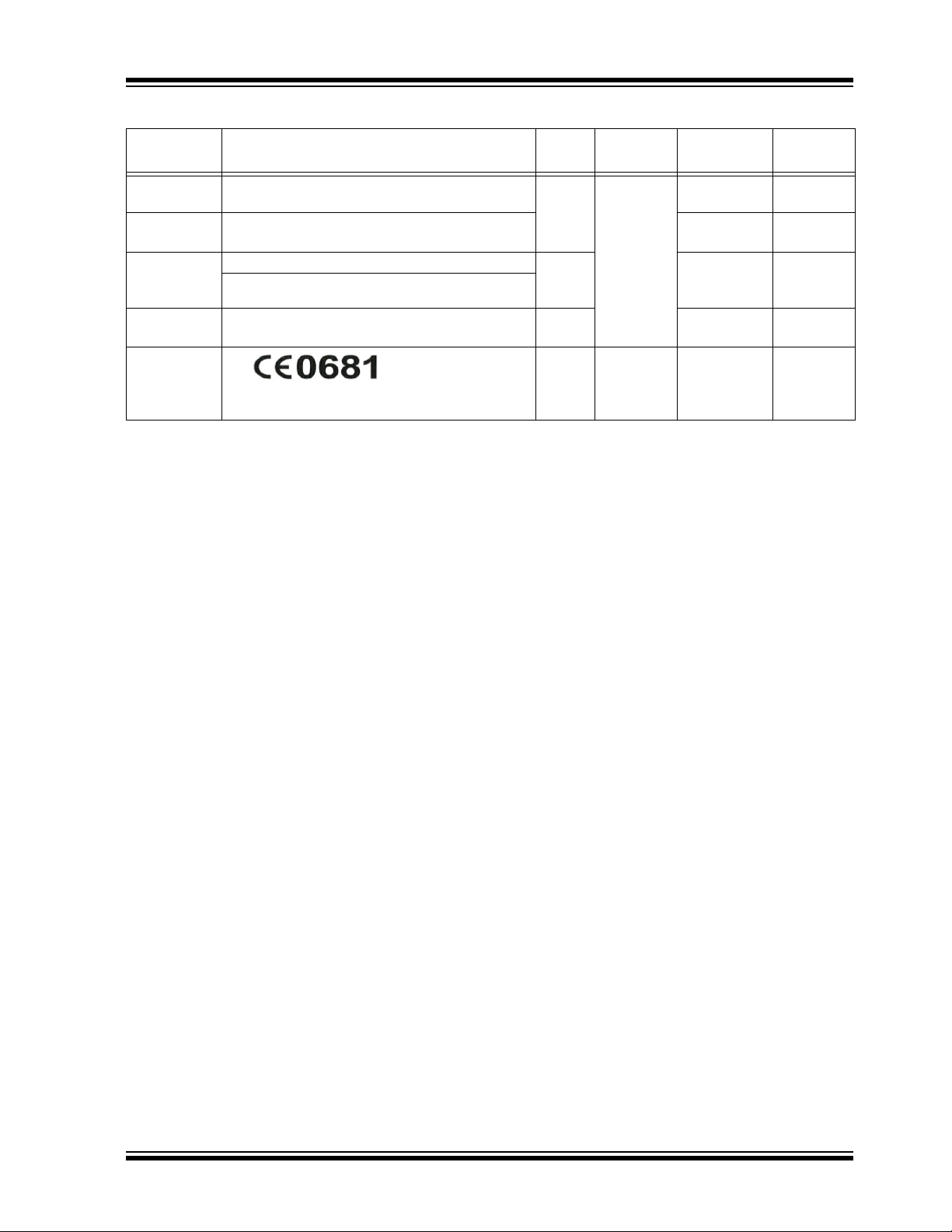
The RN42 module is an R&TTE Directive assessed
radio module that is CE marked and has been manufactured and tested with the intention of being integrated into a final product.
The RN42 module has been tested to R&TTE Directive
1999/5/EC Essential Requirements for Health and
Safety (Article (3.1(a)), Electromagnetic Compatibility
(EMC) (Article 3.1(b)), and Radio (Article 3.2) and are
summarized in Table 3-1: European Compliance Testing. A Notified Body Opinion has also been issued. All
test reports are available on the RN42 product web
page at http://www.microchip.com.
The R&TTE Compliance Association provides guidance on modular devices in document Technical
Guidance Note 01 available at
http://www.rtteca.com/html/download_area.htm.
Note: To maintain conformance to the testing
listed in Table 3-1, the module shall be
installed in accordance with the installation instructions in this data sheet and
shall not be modified.
When integrating a radio module into a
completed product the integrator
becomes the manufacturer of the final
product and is therefore responsible for
demonstrating compliance of the final
product with the essential requirements of
the R&TTE Directive.
3.3.1 LABELING AND USER
INFORMATION REQUIREMENTS
The label on the final product which contains the RN42
module must follow CE marking requirements. The
“R&TTE Compliance Association Technical Guidance
Note 01” provides guidance on final product CE marking.
3.3.2 ANTENNA REQUIREMENTS
From R&TTE Compliance Association document Te ch-
nical Guidance Note 01:
Provided the integrator installing an assessed
radio module with an integral or specific antenna
and installed in conformance with the radio module manufacturer’s installation instructions
requires no further evaluation under Article 3.2
of the R&TTE Directive and does not require further involvement of an R&TTE Directive Notified
Body for the final product. [Section 2.2.4]
3.3.3 HELPFUL WEB SITES
A document that can be used as a starting point in
understanding the use of Short Range Devices (SRD)
in Europe is the European Radio Communications
Committee (ERC) Recommendation 70-03 E, which
can be downloaded from the European Radio Communications Office (ERO) at: http://www.ero.dk.
Additional helpful web sites are:
• Radio and Telecommunications Terminal Equipment (R&TTE):
http://ec.europa.eu/enterprise/rtte/index_en.htm
• European Conference of Postal and Telecommunications Administrations (CEPT):
http://www.cept.org
• European Telecommunications Standards Institute (ETSI):
http://www.etsi.org
• European Radio Communications Office (ERO):
http://www.ero.dk
• The Radio and Telecommunications Terminal
Equipment Compliance Association (R&TTE CA):
http://www.rtteca.com
DS50002328A-page 14 2015 Microchip Technology Inc.
Page 15
RN42/RN42N
TABLE 3-1: RN42 EUROPEAN COMPLIANCE TESTING
Certification Standards Article Laboratory
Safety EN 60950-1:2006+A11:2009+A1:2010+A12:2011 [3.1(a)] Worldwide
Te st i ng
Health EN 62479:2010 W6M21402-
EMC EN 301 489-1 V1.9.2 (2011-09) [3.1(b)] W6M21402-
EN 301 489-17 V2.2.1 (2012-09)
Services
(Taiwan)
Co., Ltd.
Report
Number
W6M2140213966-L
13966-62479
13966-E-16
Date
2014-03-24
2014-03-13
2014-03-13
Radio EN 300 328 V1.8.1 (2012-06) (3.2) W6M21402-
13966-T-45
Notified Body
Opinion
3.4 Australia
The Australia radio regulations do not provide a modular approval policy similar to the United States (FCC)
and Canada (IC). However, RN42 module RF transmitter test reports can be used in part to demonstrate compliance in accordance with ACMA Radio
communications “Short Range Devices” Standard
2004 (The Short Range Devices standard calls up the
AS/NZS 4268:2008 industry standard). The RN42/
RN42N module test reports can be used as part of the
product certification and compliance folder. For more
information on the RF transmitter test reports, contact
Microchip Technology Australia sales office.
To meet overall Australian final product compliance, the
developer must construct a compliance folder containing all relevant compliance test reports e.g. RF, EMC,
electrical safety and DoC (Declaration of Conformity)
etc. It is the responsibility of the integrator to know what
is required in the compliance folder for ACMA compliance. All test reports are available on the RN42 product
web page at http://www.microchip.com. For more information on Australia compliance, refer to the Australian
Communications and Media Authority web site http://
www.acma.gov.au.
3.4.1 HELPFUL WEB SITES
The Australian Communications and Media Authority:
http://www.acma.gov.au.
—Eurofins
Product
Service
GmbH
U9M-14043736-C-V01
3.5 New Zealand
The New Zealand radio regulations do not provide a
modular approval policy similar to the United States
(FCC) and Canada (IC). However, RN42 module RF
transmitter test reports can be used in part to demonstrate compliance against the New Zealand “General
User Radio License for Short Range Devices”. New
Zealand Radio communications (Radio Standards)
Notice 2010 calls up the AS / NZS 4268:2008 industry
standard. The RN42 module test reports can be used
as part of the product certification and compliance
folder. All test reports are available on the RN42 product web page at http://www.microchip.com. For more
information on the RF transmitter test reports, contact
Microchip Technology sales office.
Information on the New Zealand short range devices
license can be found in the following web links:
• http://www.rsm.govt.nz/cms/licensees/types-ofli-
cence/general-user-licences/short-range-devices
• http://www.rsm.govt.nz/cms/policy-and-planning/
spectrum-policy-overview/legislation/gazettenotices/product-compliance/radiocommunications-radiostandards-notice-2010.
To meet overall New Zealand final product compliance,
the developer must construct a compliance folder containing all relevant compliance test reports e.g. RF,
EMC, electrical safety and DoC (Declaration of Conformity) etc. It is the responsibility of the developer to
know what is required in the compliance folder for New
Zealand Radio communications. For more information
on New Zealand compliance, refer to the web site http:/
/www.rsm.govt.nz.
2014-03-13
2014-04-15
3.5.1 HELPFUL WEB SITES
Radio Spectrum Ministry of Economic Development:
http://www.rsm.govt.nz.
2015 Microchip Technology Inc. DS50002328A-page 15
Page 16
RN42/RN42N
3.6 Japan
The RN42 module has received type certification and is
labeled with its own technical conformity mark and certification number as required to conform to the technical standards regulated by the Ministry of Internal
Affairs and Communications (MIC) of Japan pursuant
to the Radio Act of Japan.
Integration of this module into a final product does not
require additional radio certification provided installation instructions are followed and no modifications of
the module are allowed. Additional testing may be
required:
• If the host product is subject to electrical appliance safety (for example, powered from an AC
mains), the host product may require Product
Safety Electrical Appliance and Material (PSE)
testing. The integrator should contact their conformance laboratory to determine if this testing is
required.
• There is an voluntary Electromagnetic Compatibility (EMC) test for the host product administered
by VCCI: http://www.vcci.jp/vcci_e/index.html.
3.6.1 LABELING AND USER
INFORMATION REQUIREMENTS
The label on the final product which contains the RN42
module must follow Japan marking requirements. The
integrator of the module should refer to the labeling
requirements for Japan available at the Ministry of
Internal Affairs and Communications (MIC) website.
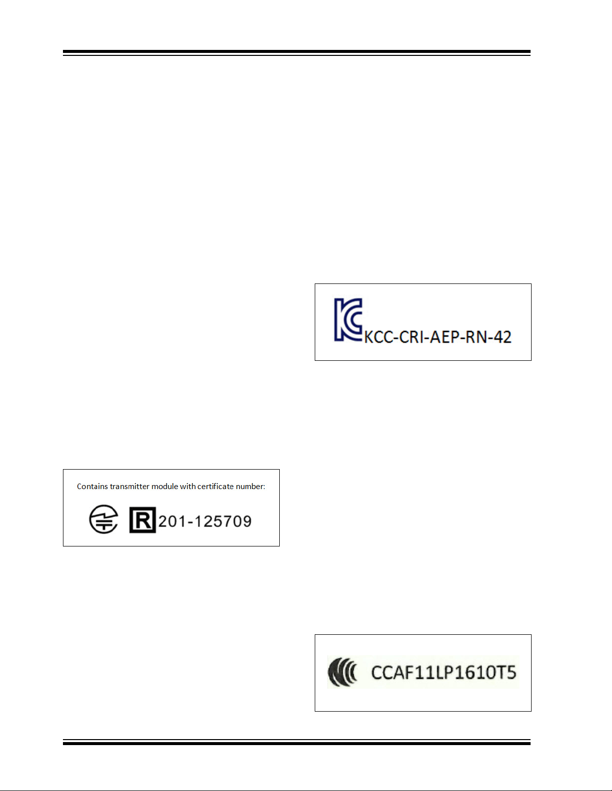
The RN42 module is labeled with its own technical conformity mark and certification number. The final product
in which this module is being used must have a label
referring to the type certified module inside:
3.6.2 HELPFUL WEB SITES
Ministry of Internal Affairs and Communications (MIC):
http://www.tele.soumu.go.jp/e/index.htm
Association of Radio Industries and Businesses
(ARIB): http://www.arib.or.jp/english
3.7 Korea
The RN42 module has received certification of conformity in accordance with the Radio Waves Act. Integration of this module into a final product does not require
additional radio certification provided installation
instructions are followed and no modifications of the
module are allowed.
3.7.1 LABELING AND USER
INFORMATION REQUIREMENTS
The label on the final product which contains the RN42
module must follow KC marking requirements. The
integrator of the module should refer to the labeling
requirements for Korea available on the Korea Communications Commission (KCC) website.
The RN42 module is labeled with its own KC mark. The
final product requires the KC mark and certificate number of the module:
3.7.2 HELPFUL WEB SITES
Korea Communications Commission (KCC):
http://www.kcc.go.kr
National Radio Research Agency (RRA):
http://rra.go.kr
3.8 Taiwan
The RN42 module has received compliance approval
in accordance with the Telecommunications Act. Customers seeking to use the compliance approval in their
product should contact Microchip Technology sales or
distribution partners to obtain a Letter of Authority.
Integration of this module into a final product does not
require additional radio certification provided installation instructions are followed and no modifications of
the module are allowed.
3.8.1 LABELING AND USER
INFORMATION REQUIREMENTS
The RN42 module is labeled with its own NCC mark
and certificate number as below:
DS50002328A-page 16 2015 Microchip Technology Inc.
Page 17
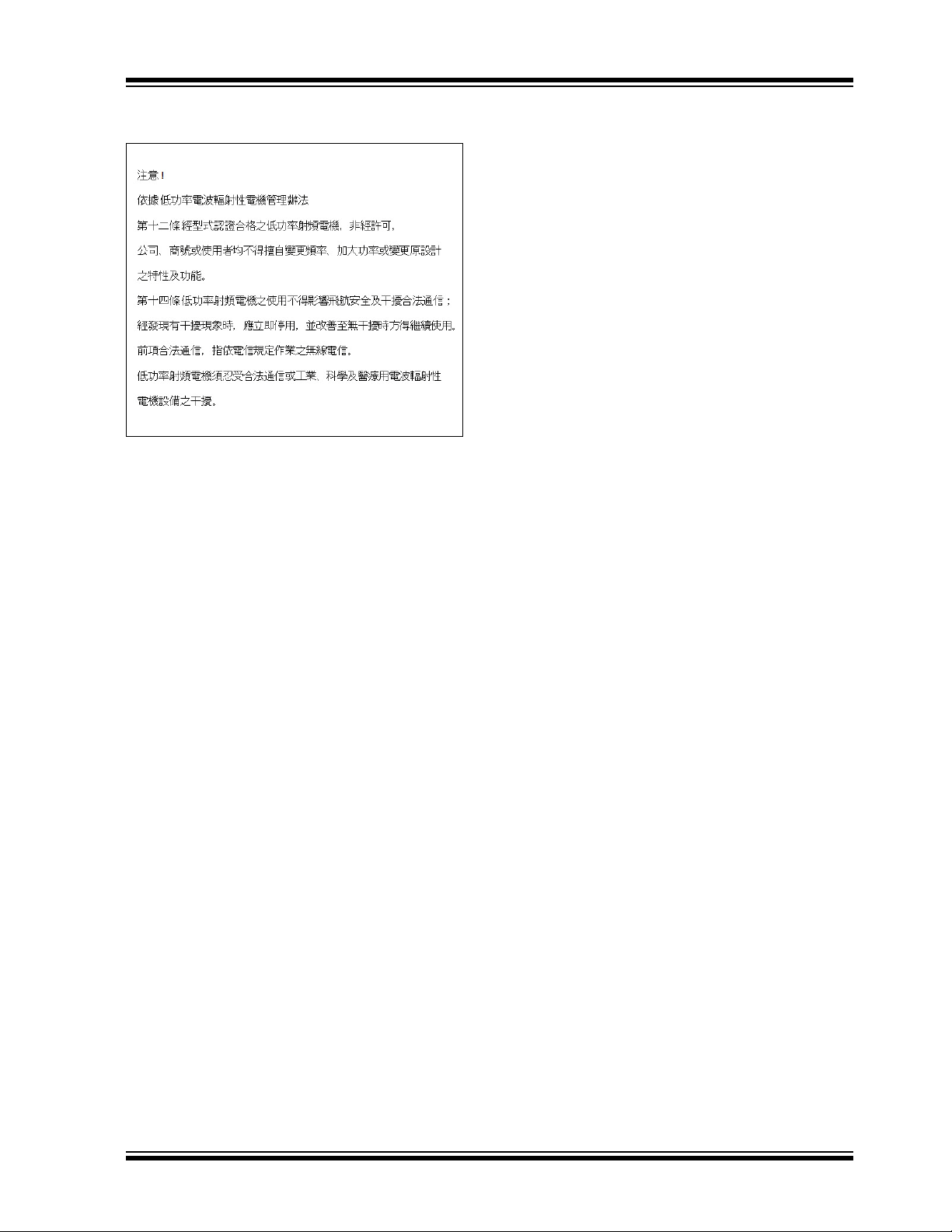
The user’s manual should contain below warning (for
RF device) in traditional Chinese:
3.8.2 HELPFUL WEB SITES
National Communications Commission (NCC):
http://www.ncc.gov.tw
RN42/RN42N
2015 Microchip Technology Inc. DS50002328A-page 17
Page 18
RN42/RN42N
4.0 ORDERING INFORMATION
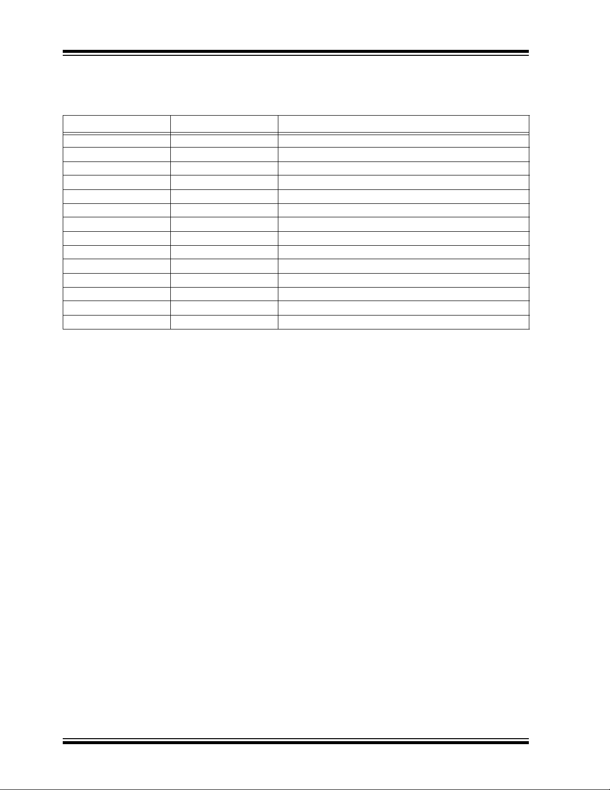
Table 4-1 provides ordering information for the RN42 module.
TABLE 4-1: ORDERING INFORMATION
Part Number
RN42-I/RM 6.15 Class 2, 2.1+EDR, SPP profile
RN42-I/RM615 6.15 Class 2, 2.1+EDR, SPP profile
RN42-I/RM477 4.77 Class 2, 2.1+EDR, SPP profile
RN42HCI-I/RM N/A Class 2, 2.0+EDR, HCI over UART
RN42HID-I/RM 6.11 Class 2, 2.1+EDR, HID and SPP profiles
RN42U-I/RM N/A Class 2, 2.0+EDR, HCI over USB
RN42APL-I/RM 5.45 Class 2, 2.1+EDR, SPP and MFi profiles
RN42APL-I/RM545 5.45 Class 2, 2.1+EDR, SPP and MFi profiles
RN42APL-I/RM543 5.43 Class 2, 2.1+EDR, SPP and MFi profiles
RN42N-I/RM 6.15 Class 2, 2.1+EDR, SPP profile
RN42NHCI-I/RM N/A Class 2, 2.0+EDR, HCI over UART
RN42NHID-I/RM 6.11 Class 2, 2.1+EDR, HID and SPP profiles
RN42NU-I/RM N/A Class 2, 2.0+EDR, HCI over USB
RN42NAPL-I/RM 5.45 Class 2, 2.1+EDR, SPP and MFi profiles
Note 1: For other configurations, contact Microchip drectly.
2: It is highly recommended that customers order part numbers by specific firmware version when available to
Go to http://www.microchip.com for current pricing and a list of distributors carrying Microchip products.
(1)
ensure consistent receipt of their designed-in firmware version. Information on firmware versions can be
found on the RN42/RN42N product web page and the “Bluetooth Data Module Command Reference and
Advanced Information User’s Guide”.
Firmware
(2)
(1)
Description
DS50002328A-page 18 2015 Microchip Technology Inc.
Page 19

APPENDIX A: REVISION HISTORY
Revision A (January 2015)
This is the initial released version of the document in
the Microchip format. This replaces Roving Networks
RN42/RN42N Data Sheet.
RN42/RN42N
2015 Microchip Technology Inc. DS50002328A-page 19
Page 20

RN42/RN42N
NOTES:
DS50002328A-page 20 2015 Microchip Technology Inc.
Page 21

RN42/RN42N
THE MICROCHIP WEB SITE
Microchip provides online support via our WWW site at
www.microchip.com. This web site is used as a means
to make files and information easily available to
customers. Accessible by using your favorite Internet
browser, the web site contains the following
information:
• Product Support – Data sheets and errata,
application notes and sample programs, design
resources, user’s guides and hardware support
documents, latest software releases and archived
software
• General Technical Support – Frequently Asked
Questions (FAQ), technical support requests,
online discussion groups, Microchip consultant
program member listing
• Business of Microchip – Product selector and
ordering guides, latest Microchip press releases,
listing of seminars and events, listings of
Microchip sales offices, distributors and factory
representatives
CUSTOMER CHANGE NOTIFICATION
SERVICE
CUSTOMER SUPPORT
Users of Microchip products can receive assistance
through several channels:
• Distributor or Representative
• Local Sales Office
• Field Application Engineer (FAE)
• Technical Support
Customers should contact their distributor,
representative or Field Application Engineer (FAE) for
support. Local sales offices are also available to help
customers. A listing of sales offices and locations is
included in the back of this document.
Technical support is available through the web site
at: http://microchip.com/support
Microchip’s customer notification service helps keep
customers current on Microchip products. Subscribers
will receive e-mail notification whenever there are
changes, updates, revisions or errata related to a
specified product family or development tool of interest.
To register, access the Microchip web site at
www.microchip.com. Under “Support”, click on
“Customer Change Notification” and follow the
registration instructions.
2015 Microchip Technology Inc. DS50002328A-page 21
Page 22

RN42/RN42N
NOTES:
DS50002328A-page 22 2015 Microchip Technology Inc.
Page 23
RN42/RN42N
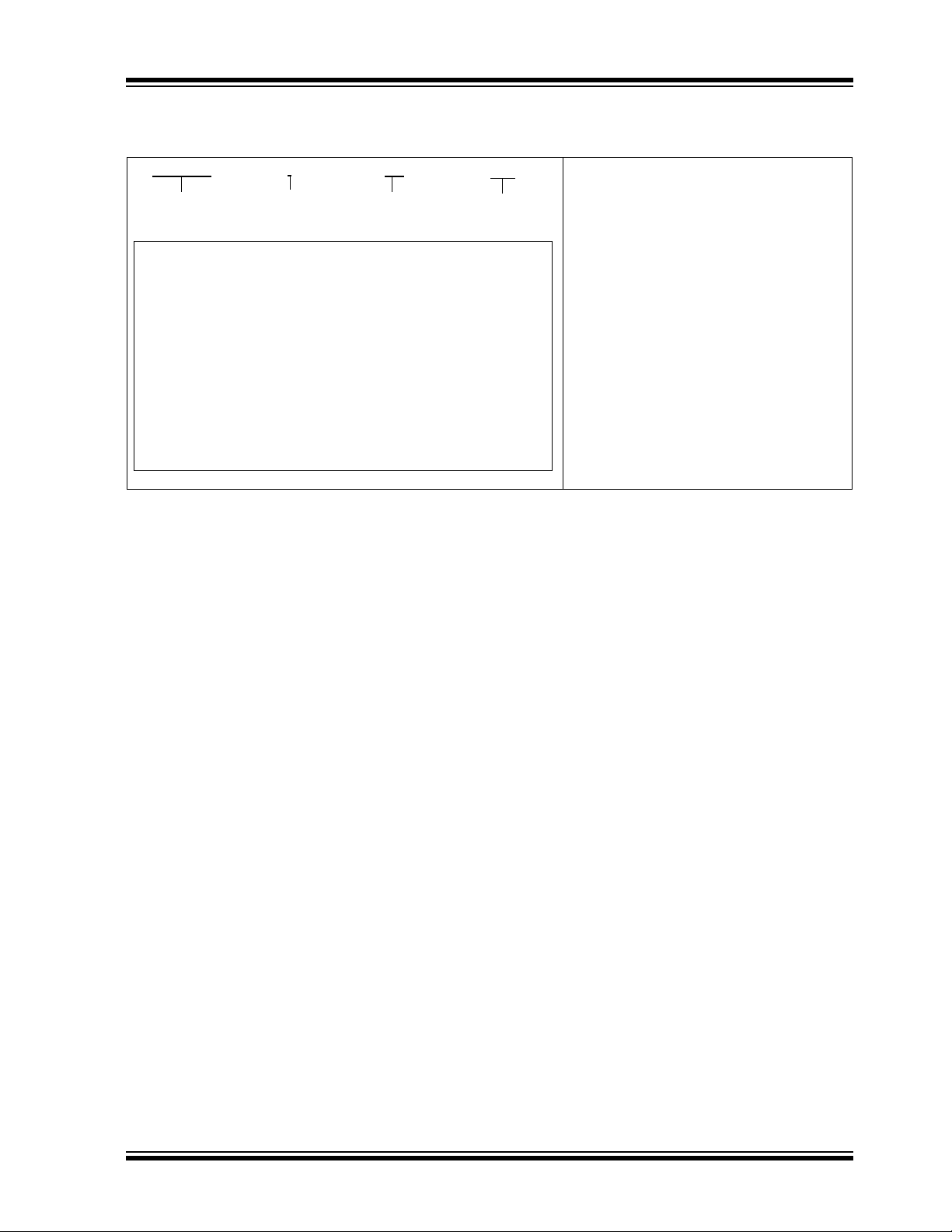
Device: RN42 : UART, Integral Antenna
RN42N : UART, External Antenna
RN42HCI: UART, HCI firmware, Integral Antenna
RN42U : USB, Integral Antenna
RN42APL: UART, MFi firmware
Temperature Range: I = -40°C to +85°C
Package: * RM = Radio Module
*All package offerings are Pb (Lead) Free
Examples:
a) RN42-I/RM: Integral Antenna,
Firmware version 6.15
b) RN42-I/RM615: Integral Antenna,
Firmware version 6.15
c) RN42APL-I/RM: Integral Antenna,
Firmware version 5.45,
SPP and MFi firmware
d) RN42N-I/RM: External Antenna,
Firmware version 6.15
PART NO.
I
RM
Package
Temperature
Range
Device
XXX
Firmware
Revision
Number
PRODUCT IDENTIFICATION SYSTEM
To order or obtain information, e.g., on pricing or delivery, refer to the factory or the listed sales office.
2015 Microchip Technology Inc. DS50002328A-page 23
Page 24

RN42/RN42N
NOTES:
DS50002328A-page 24 2015 Microchip Technology Inc.
Page 25

YSTEM
CERTIFIEDBYDNV
== ISO/TS16949==
Note the following details of the code protection feature on Microchip devices:
• Microchip products meet the specification contained in their particular Microchip Data Sheet.
• Microchip believes that its family of products is one of the most secure families of its kind on the market today, when used in the
intended manner and under normal conditions.
• There are dishonest and possibly illegal methods used to breach the code protection feature. All of these methods, to our
knowledge, require using the Microchip products in a manner outside the operating specifications contained in Microchip’s Data
Sheets. Most likely, the person doing so is engaged in theft of intellectual property.
• Microchip is willing to work with the customer who is concerned about the integrity of their code.
• Neither Microchip nor any other semiconductor manufacturer can guarantee the security of their code. Code protection does not
mean that we are guaranteeing the product as “unbreakable.”
Code protection is constantly evolving. We at Microchip are committed to continuously improving the code protection features of our
products. Attempts to break Microchip’s code protection feature may be a violation of the Digital Millennium Copyright Act. If such acts
allow unauthorized access to your software or other copyrighted work, you may have a right to sue for relief under that Act.
Information contained in this publication regarding device
applications and the like is provided only for your convenience
and may be superseded by updates. It is your responsibility to
ensure that your application meets with your specifications.
MICROCHIP MAKES NO REPRESENTATIONS OR
WARRANTIES OF ANY KIND WHETHER EXPRESS OR
IMPLIED, WRITTEN OR ORAL, STATUTORY OR
OTHERWISE, RELATED TO THE INFORMATION,
INCLUDING BUT NOT LIMITED TO ITS CONDITION,
QUALITY, PERFORMANCE, MERCHANTABILITY OR
FITNESS FOR PURPOSE. Microchip disclaims all liability
arising from this information and its use. Use of Microchip
devices in life support and/or safety applications is entirely at
the buyer’s risk, and the buyer agrees to defend, indemnify and
hold harmless Microchip from any and all damages, claims,
suits, or expenses resulting from such use. No licenses are
conveyed, implicitly or otherwise, under any Microchip
intellectual property rights.
Trademarks
The Microchip name and logo, the Microchip logo, dsPIC,
FlashFlex, flexPWR, JukeBlox, K
LANCheck, MediaLB, MOST, MOST logo, MPLAB,
OptoLyzer, PIC, PICSTART, PIC
SST, SST Logo, SuperFlash and UNI/O are registered
trademarks of Microchip Technology Incorporated in the
U.S.A. and other countries.
The Embedded Control Solutions Company and mTouch are
registered trademarks of Microchip Technology Incorporated
in the U.S.A.
Analog-for-the-Digital Age, BodyCom, chipKIT, chipKIT logo,
CodeGuard, dsPICDEM, dsPICDEM.net, ECAN, In-Circuit
Serial Programming, ICSP, Inter-Chip Connectivity, KleerNet,
KleerNet logo, MiWi, MPASM, MPF, MPLAB Certified logo,
MPLIB, MPLINK, MultiTRAK, NetDetach, Omniscient Code
Generation, PICDEM, PICDEM.net, PICkit, PICtail,
RightTouch logo, REAL ICE, SQI, Serial Quad I/O, Total
Endurance, TSHARC, USBCheck, VariSense, ViewSpan,
WiperLock, Wireless DNA, and ZENA are trademarks of
Microchip Technology Incorporated in the U.S.A. and other
countries.
SQTP is a service mark of Microchip Technology Incorporated
in the U.S.A.
Silicon Storage Technology is a registered trademark of
Microchip Technology Inc. in other countries.
GestIC is a registered trademarks of Microchip Technology
Germany II GmbH & Co. KG, a subsidiary of Microchip
Technology Inc., in other countries.
All other trademarks mentioned herein are property of their
respective companies.
© 2015, Microchip Technology Incorporated, Printed in the
U.S.A., All Rights Reserved.
ISBN: 978-1-63276-903-9
EELOQ, KEELOQ logo, Kleer,
32
logo, RightTouch, SpyNIC,
QUALITYMANAGEMENTS
2015 Microchip Technology Inc. DS50002328A-page 25
Microchip received ISO/TS-16949:2009 certification for its worldwide
headquarters, design and wafer fabrication facilities in Chandler and
Tempe, Arizona; Gresham, Oregon and design centers in California
and India. The Company’s quality system processes and procedures
are for its PIC
devices, Serial EEPROMs, microperipherals, nonvolatile memory and
analog products. In addition, Microchip’s quality system for the design
and manufacture of development systems is ISO 9001:2000 certified.
®
MCUs and dsPIC® DSCs, KEELOQ
®
code hopping
Page 26

Worldwide Sales and Service
AMERICAS
Corporate Office
2355 West Chandler Blvd.
Chandler, AZ 85224-6199
Tel: 480-792-7200
Fax: 480-792-7277
Technical Support:
http://www.microchip.com/
support
Web Address:
www.microchip.com
Atlanta
Duluth, GA
Tel: 678-957-9614
Fax: 678-957-1455
Austin, TX
Tel: 512-257-3370
Boston
Westborough, MA
Tel: 774-760-0087
Fax: 774-760-0088
Chicago
Itasca, IL
Tel: 630-285-0071
Fax: 630-285-0075
Cleveland
Independence, OH
Tel: 216-447-0464
Fax: 216-447-0643
Dallas
Addison, TX
Tel: 972-818-7423
Fax: 972-818-2924
Detroit
Novi, MI
Tel: 248-848-4000
Houston, TX
Tel: 281-894-5983
Indianapolis
Noblesville, IN
Tel: 317-773-8323
Fax: 317-773-5453
Los Angeles
Mission Viejo, CA
Tel: 949-462-9523
Fax: 949-462-9608
New York, NY
Tel: 631-435-6000
San Jose, CA
Tel: 408-735-9110
Canada - Toronto
Tel: 905-673-0699
Fax: 905-673-6509
ASIA/PACIFIC
Asia Pacific Office
Suites 3707-14, 37th Floor
Tower 6, The Gateway
Harbour City, Kowloon
Hong Kong
Tel: 852-2943-5100
Fax: 852-2401-3431
Australia - Sydney
Tel: 61-2-9868-6733
Fax: 61-2-9868-6755
China - Beijing
Tel: 86-10-8569-7000
Fax: 86-10-8528-2104
China - Chengdu
Tel: 86-28-8665-5511
Fax: 86-28-8665-7889
China - Chongqing
Tel: 86-23-8980-9588
Fax: 86-23-8980-9500
China - Hangzhou
Tel: 86-571-8792-8115
Fax: 86-571-8792-8116
China - Hong Kong SAR
Tel: 852-2943-5100
Fax: 852-2401-3431
China - Nanjing
Tel: 86-25-8473-2460
Fax: 86-25-8473-2470
China - Qingdao
Tel: 86-532-8502-7355
Fax: 86-532-8502-7205
China - Shanghai
Tel: 86-21-5407-5533
Fax: 86-21-5407-5066
China - Shenyang
Tel: 86-24-2334-2829
Fax: 86-24-2334-2393
China - Shenzhen
Tel: 86-755-8864-2200
Fax: 86-755-8203-1760
China - Wuhan
Tel: 86-27-5980-5300
Fax: 86-27-5980-5118
China - Xian
Tel: 86-29-8833-7252
Fax: 86-29-8833-7256
China - Xiamen
Tel: 86-592-2388138
Fax: 86-592-2388130
China - Zhuhai
Tel: 86-756-3210040
Fax: 86-756-3210049
ASIA/PACIFIC
India - Bangalore
Tel: 91-80-3090-4444
Fax: 91-80-3090-4123
India - New Delhi
Tel: 91-11-4160-8631
Fax: 91-11-4160-8632
India - Pune
Tel: 91-20-3019-1500
Japan - Osaka
Tel: 81-6-6152-7160
Fax: 81-6-6152-9310
Japan - Tokyo
Tel: 81-3-6880- 3770
Fax: 81-3-6880-3771
Korea - Daegu
Tel: 82-53-744-4301
Fax: 82-53-744-4302
Korea - Seoul
Tel: 82-2-554-7200
Fax: 82-2-558-5932 or
82-2-558-5934
Malaysia - Kuala Lumpur
Tel: 60-3-6201-9857
Fax: 60-3-6201-9859
Malaysia - Penang
Tel: 60-4-227-8870
Fax: 60-4-227-4068
Philippines - Manila
Tel: 63-2-634-9065
Fax: 63-2-634-9069
Singapore
Tel: 65-6334-8870
Fax: 65-6334-8850
Taiwan - Hsin Chu
Tel: 886-3-5778-366
Fax: 886-3-5770-955
Taiwan - Kaohsiung
Tel: 886-7-213-7830
Taiwan - Taipei
Tel: 886-2-2508-8600
Fax: 886-2-2508-0102
Thailand - Bangkok
Tel: 66-2-694-1351
Fax: 66-2-694-1350
EUROPE
Austria - Wels
Tel: 43-7242-2244-39
Fax: 43-7242-2244-393
Denmark - Copenhagen
Tel: 45-4450-2828
Fax: 45-4485-2829
France - Paris
Tel: 33-1-69-53-63-20
Fax: 33-1-69-30-90-79
Germany - Dusseldorf
Tel: 49-2129-3766400
Germany - Munich
Tel: 49-89-627-144-0
Fax: 49-89-627-144-44
Germany - Pforzheim
Tel: 49-7231-424750
Italy - Milan
Tel: 39-0331-742611
Fax: 39-0331-466781
Italy - Venice
Tel: 39-049-7625286
Netherlands - Drunen
Tel: 31-416-690399
Fax: 31-416-690340
Poland - Warsaw
Tel: 48-22-3325737
Spain - Madrid
Tel: 34-91-708-08-90
Fax: 34-91-708-08-91
Sweden - Stockholm
Tel: 46-8-5090-4654
UK - Wokingham
Tel: 44-118-921-5800
Fax: 44-118-921-5820
03/25/14
DS50002328A-page 26 2015 Microchip Technology Inc.
 Loading...