

INFINEON BSS131 User Manual
Type
BSS131
SIPMOS® Small-Signal-Transistor
Feature
• N-Channel
• Enhancement mode
Product Summary
V
DS
R
DS(on),max
I
D
• Logic level
• dv /dt rated
• Pb-free lead-plating; RoHS compliant
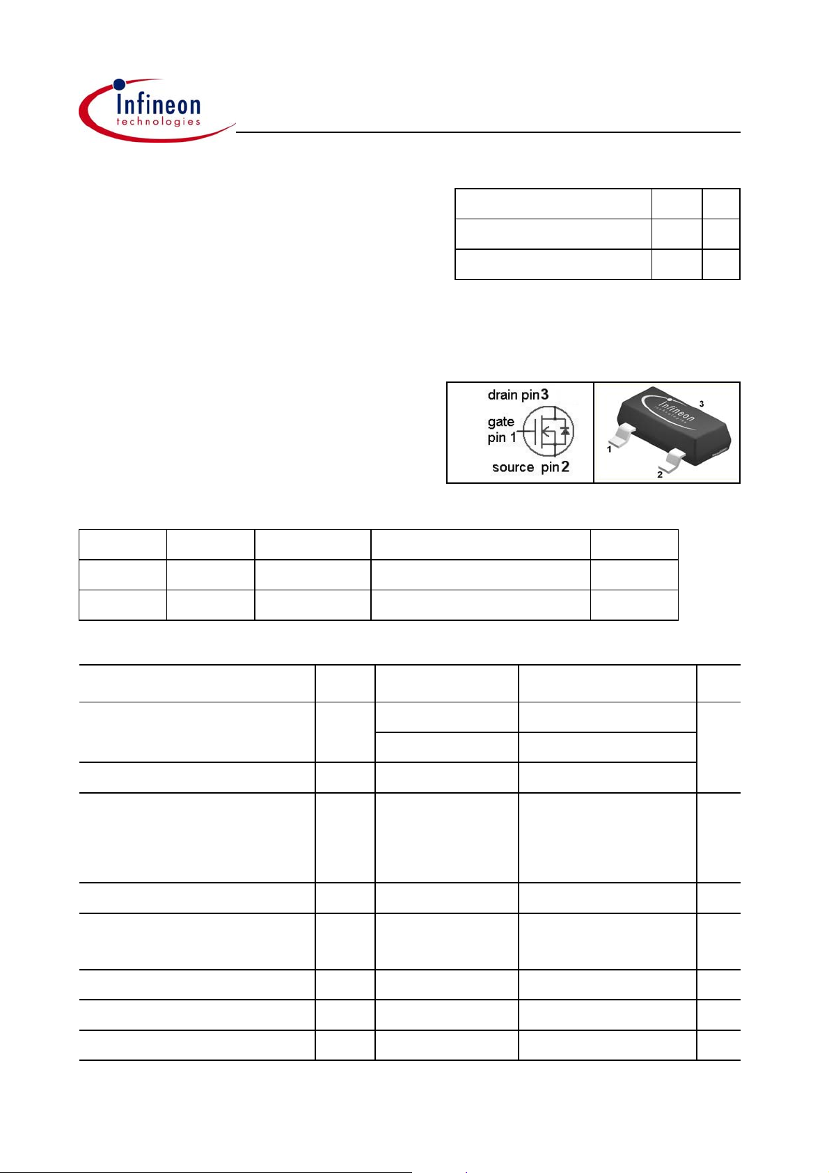
PG-SOT-23
Type Package Ordering Code Tape and Reel Information Marking
240 V
14
0.1 A
Ω
BSS131 PG-SOT23 Q62702-S565 E6327 SRs
BSS131 PG-SOT23 Q67000-S229 E6433 SRs
Maximum ratings, at T
Parameter Symbol Conditions Unit
Continuous drain current
Pulsed drain current
Reverse diode dv /dt dv /dt
Gate source voltage
ESD sensitivity (HBM) as per
MIL-STD 883
=25 °C, unless otherwise specified
j
I
D
I
D,pulse
TA=25 °C
T
=70 °C
A
TA=25 °C
=0.1 A, VDS=192 V,
I
D
di /dt =200 A/µs,
T
=150 °C
j,max
V
GS
Value
0.11 A
0.09
0.4
6 kV/µs
±20 V
Class 1a
Power dissipation
Operating and storage temperature
P
tot
T
, T
j
stg
TA=25 °C
0.36 W
-55 ... 150 °C
IEC climatic category; DIN IEC 68-1 55/150/56
Rev. 2.1 page 1 2005-02-24
BSS131
Parameter Symbol Conditions Unit
Values
min. typ. max.
Thermal characteristics
Thermal resistance,
junction - minimal footprint
Electrical characteristics, at T
R
thJA
=25 °C, unless otherwise specified
j
- - 350 K/W
Static characteristics
Drain-source breakdown voltage
Gate threshold voltage
Drain-source leakage current
V
(BR)DSSVGS
V
GS(th)
I
D (off)
=0 V, ID=250 µA
VDS=0 V, ID=56 µA
VDS=240 V, VGS=0 V,
T
=25 °C
j
V
=240 V, VGS=0 V,
DS
T
=150 °C
j
240 - - V
0.8 1.4 1.8
- - 0.01 µA
--5
Gate-source leakage current
Drain-source on-state resistance
Transconductance
I
R
g
GSS
DS(on)
fs
VGS=20 V, VDS=0 V
VGS=4.5 V, ID=0.09 A
V
=10 V, ID=0.1 A
GS
|VDS|>2|ID|R
I
=0.08 A
D
DS(on)max
- - 10 nA
- 9.07 20
- 7.7 14
,
0.06 0.13 - S
Ω
Rev. 2.1 page 2 2005-02-24

BSS131
y
Parameter Symbol Conditions Unit
Values
min. typ. max.
namic characteristics
D
Input capacitance
Output capacitance
Reverse transfer capacitance
Turn-on delay time
Rise time
Turn-off delay time
Fall time
C
C
C
t
t
t
t
iss
oss
rss
d(on)
r
d(off)
f
V
=0 V, VDS=25 V,
GS
f =1 MHz
V
=120 V,
DD
V
=10 V, ID=0.1 A,
GS
R
=6 Ω
G
-5877pF
- 7.3 10
- 2.8 4.2
- 3.3 5.0 ns
- 3.1 4.6
- 13.7 20
- 64.5 97
Gate Charge Characteristics
Gate to source charge
Gate to drain charge
Gate charge total
Q
gs
Q
gd
Q
g
V
=192 V, ID=0.1 A,
DD
V
=0 to 10 V
GS
- 0.16 0.22 nC
- 0.8 1.2
- 2.1 3.1
Gate plateau voltage
Reverse Diode
Diode continous forward current
Diode pulse current
Diode forward voltage
Reverse recovery time
Reverse recovery charge
V
plateau
I
S
I
S,pulse
V
SD
t
rr
Q
rr
=25 °C
T
A
VGS=0 V, IF=0.1 A,
T
=25 °C
j
=120 V, IF=0.1 A,
V
R
di
/dt =100 A/µs
F
- 2.90 - V
- - 0.11 A
- - 0.43
- 0.81 1.2 V
- 42.9 64.3 ns
- 22.6 34 nC
Rev. 2.1 page 3 2005-02-24
 Loading...