

INFINEON BSS123 User Manual
Rev. 1.2
DS
DS(on)
D
j
GS
j
stg
BSS123
SIPMOS Small-Signal-Transistor
Feature
• N-Channel
• Enhancement mode
• Logic Level
• dv/dt rated
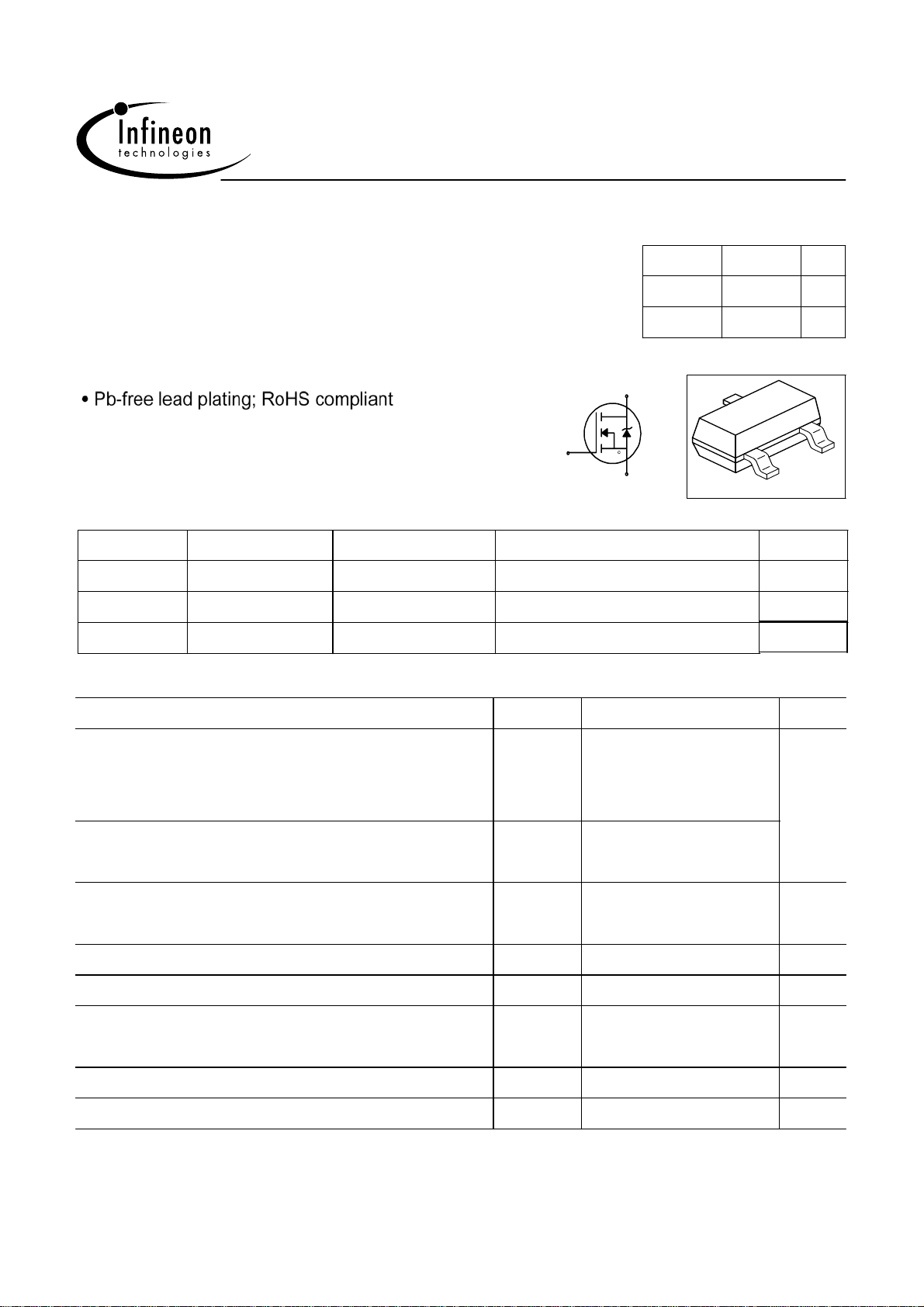
Gate
pin1
Type
BSS123
Package
PG-SOT23
Ordering Code
Q62702-S512
BSS123 PG-SOT23 Q67000-S245
BSS123 PG-SOT23
SP000084574
Tape and Reel Information
E6327: 3000 pcs/reel
E6433: 10000 pcs/reel
L6327: 3000 pcs/reel
Product Summary
V
R
I
Drain
pin 3
Source
pin 2
100 V
6 Ω
0.17 A
PG-SOT23
3
1
VPS05161
Marking
SAs
SAs
SAs
2
Maximum Ratings, at
Parameter
Continuous drain current
TA=25°C
T
=70°C
A
Pulsed drain current
TA=25°C
Reverse diode dv/dt
IS=0.17A, VDS=80V, di/dt=200A/µs, T
Gate source voltage V
T
= 25 °C, unless otherwise specified
Symbol Value Unit
I
D
I
D puls
dv/dt
=150°C
jmax
0.17
0.14
0.68
6 kV/µs
±20
ESD Sensitivity (HBM) as per MIL-STD 883 Class 1a
Power dissipation
TA=25°C
Operating and storage temperature T
IEC climatic category; DIN IEC 68-1
P
tot
,
T
0.36 W
-55... +150
55/150/56
A
V
°C
Page 1
2005-07-21

Rev. 1.2
j
BSS123
Thermal Characteristics
Parameter Symbol Values Unit
min. typ. max.
Characteristics
Thermal resistance, junction - ambient
R
thJA
- - 350 K/W
at minimum footprint
Electrical Characteristics, at
T
= 25 °C, unless otherwise specified
Parameter Symbol Values Unit
min. typ. max.
Static Characteristics
Drain-source breakdown voltage
VGS=0, ID=250µA
Gate threshold voltage,
I
=50µA
D
V
GS
=
V
Zero gate voltage drain current
VDS=100V, VGS=0, Tj=25°C
V
=100V, VGS=0, Tj=150°C
DS
Gate-source leakage current
VGS=20V, VDS=0
DS
V
(BR)DSS
V
GS(th)
I
DSS
I
GSS
100 - - V
0.8 1.4 1.8
-
-
-
-
0.01
5
- - 10 nA
µA
Drain-source on-state resistance
VGS=4.5V, ID=0.13A
Drain-source on-state resistance
VGS=10V, ID=0.17A
Page 2
R
DS(on)
R
DS(on)
- 4 10
- 3 6
2005-07-21
Ω

Rev. 1.2
j
iss
oss
rss
d(on)
r
d(off)
f
gs
gd
(plateau)
Inv. diode direct current, pulsed
SM
SD
rr
rr
BSS123
Electrical Characteristics, at
T
= 25 °C, unless otherwise specified
Parameter Symbol Conditions Values Unit
min. typ. max.
Dynamic Characteristics
Transconductance g
Input capacitance C
Output capacitance C
Reverse transfer capacitance C
Turn-on delay time t
Rise time t
Turn-off delay time t
Fall time t
fs
VDS≥2*ID*R
I
=0.14A
D
VGS=0, VDS=25V,
f=1MHz
VDD=50V, VGS=10V,
I
=0.17A, RG=6Ω
D
DS(on)max
,
0.09 0.19 - S
- 55 69 pF
- 8.5 10.6
- 5 6.3
- 2.7 4 ns
- 3.1 4.6
- 9.9 14.8
- 25 37
Gate Charge Characteristics
Gate to source charge Q
VDD=80V, ID=0.17A
- 0.055 0.082 nC
Gate to drain charge Q
Gate charge total Q
Gate plateau voltage V
Reverse Diode
Inverse diode continuous
I
forward current
I
Inverse diode forward voltage V
Reverse recovery time t
Reverse recovery charge Q
- 0.77 1.15
g
S
VDD=80V, ID=0.17A,
V
=0 to 10V
GS
VDD=80V, ID = 0.17 A
TA=25°C
- 1.78 2.67
- 2.6 - V
- - 0.17 A
- - 0.68
VGS=0, IF = I
VR=50V, I
di
/dt=100A/µs
F
=
F
S
lS,
- 0.81 1.2 V
- 27.6 41.1 ns
- 10.5 15.7 nC
Page 3
2005-07-21
 Loading...