

•
High-side switch
•
Short-circuit protection
•
Input protection
•
Overtemperature protection with hysteresis
•
Overload protection
•
Overvoltage protection
•
Switching inductive load
•
Clamp of negative output voltage with inductive loads
•
Undervoltage shutdown
•
Maximum current internally limited
•
Electrostatic discharge (ESD) protection
•
Reverse battery protection
• AEC qualified
Package: SOT 223
• Green product (RoHS compliant)
1
)
Smart High-Side Power Switch
BSP452
SOT-223
1
SOT-223
PG-SOT-223
Type
BSP 452
Ordering code
Q67000-S271
Application
•
µ
C compatible power switch for 12 V DC grounded loads
•
All types of resistive, inductive and capacitive loads
•
Replaces electromechanical relays and discrete circuits
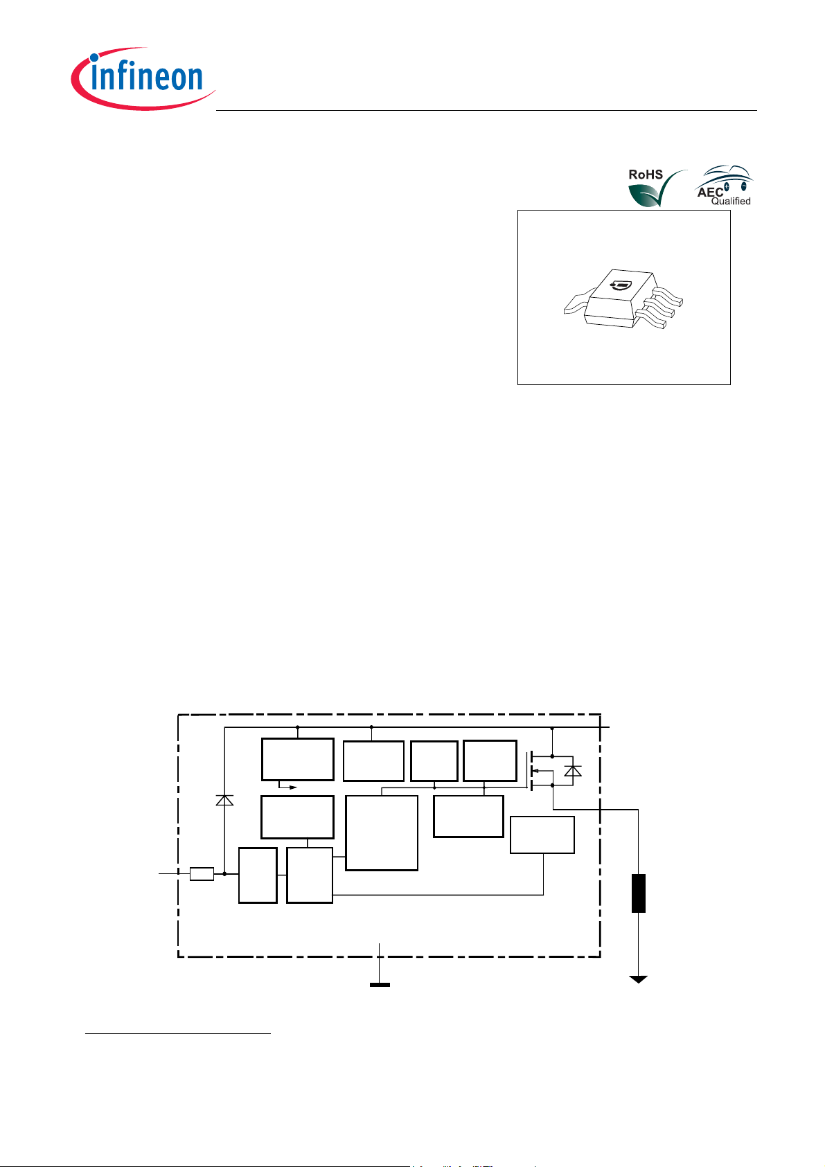
General Description
N channel vertical power FET with charge pump, ground referenced CMOS compatible input,monolithically
integrated in Smart SIPMOS technology. Fully protected by embedded protection functions.
Blockdiagramm:
+ V
bb
Voltage
source
ESDDiode
R
in
IN
3
ESD
V
Voltage
sensor
Logic
Logic
Overvoltage
protection
Charge pump
Level shifter
Rectifier
Current
limit
Gate
protection
Limit for
unclamped
ind. loads
Temperature
sensor
4
OUT
1
Load
GND
miniPROFET
2
Load GND
1
)
With resistor R
limited by connected load.
=150 Ω in GND connection, resistor in series with IN connections reverse load current
GND
Signal GND
Data Sheet 1 V1.0, 2007-05-25
Smart High-Side Power Switch
)
BSP452
Pin Symbol Function
1 OUT O Output to the load
2 GND - Logic ground
3 IN I Input, activates the power switch in case of logical high signal
4 Vbb + Positive power supply voltage
Maximum Ratings at
T
j = 25 °C unless otherwise specified
Parameter Symbol Values Unit
Supply voltage
Load current self-limited
2
Maximum input voltage
)
Maximum input current
Inductive load switch-off energy dissipation,
single pulse
I
L = 0.5A , TA = 150°C
V
I
V
I
E
bb
L
IN
IN
AS
-5.0...
40 V
I
L(SC
V
bb
±5 mA
0.5 J
(not tested, specified by design)
Load dump protection
R
=2Ω ,
I
t
=400ms, IN= low or high,
d
3
)
V
LoadDump
=
U
+
V
A
s
U
=13,5V
A
R
R
L
L
= 24Ω
= 80Ω
V
Load dump
4
)
60
80
(not tested, specified by design)
5
Electrostatic discharge capability (ESD)
Operating temperature range
Storage temperature range
6
Max. power dissipation (DC)
)
)
PIN 3
PIN 1,2,4
T
A = 25 °C
V
T
T
P
ESD
j
stg
tot
±1
±2
-40 ...+150
-55 ...+150
1.8 W
A
V
V
kV
°C
Thermal resistance chip - soldering point:
chip - ambient:
2
)
At VIN > Vbb, the input current is not allowed to exceed ±5 mA.
3
)
Supply voltages higher than V
A resistor for the protection of the input is integrated.
4
)
V
Load dump
5
)
HBM according to MIL-STD 883D, Methode 3015.7
6
)
BSP 452 on epoxy pcb 40 mm x 40 mm x 1.5 mm with 6 cm2 copper area for Vbb connection
Data Sheet 2 V1.0, 2007-05-25
is setup without the DUT connected to the generator per ISO 7637-1 and DIN 40839
require an external current limit for the GND pin, e.g. with a 150 Ω resistor in the GND connection
bb(AZ)
R
thJS
6)
R
thJA
770K/W
Smart High-Side Power Switch
BSP452
Electrical Characteristics
Parameter and Conditions Symbol Values Unit
at
T
= 25 °C,
j
V
= 13.5V unless otherwise specified
bb
min typ max
Load Switching Capabilities and Characteristics
On-state resistance (pin 4 to 1)
--
I
= 0.5 A,
L
Nominal load current (pin 4 to 1)
ISO Standard:
T
= 85 °C
S
V
in = high
V
ON =
V
bb
T
= 25°C
j
T
= 150°C
7
)
V
OUT
= 0.5 V
-
j
Turn-on time to 90%
Turn-off time to 10%
R
= 24 Ω
L
Slew rate on
10 to 30%
V
OUT
,
R
= 24 Ω
L
Slew rate off
70 to 40%
V
OUT
,
R
L
= 24 Ω
V
V
OUT
OUT
R
ON
I
L(ISO)
t
on
t
off
V
d
V
-d
/dt
/dt
on
off
0.16
--
--
0.7 -- -- A
--
--
60
60
-- 2 4 V/µs
-- 2 4 V/µs
0.2
0.4
100
150
Ω
µs
Input
Allowable input voltage range, (pin 3 to 2)
Input turn-on threshold voltage
T
= -40...+150°C
j
Input turn-off threshold voltage
T
= -40...+150°C
j
Input threshold hysteresis
Off state input current (pin 3)
On state input current (pin 3)
V
V
IN(off) = 1.2 V
T
= -40...+150°C
j
IN(on) = 3.0 V to
T
= -40...+150°C
j
Input resistance
7
)
I
L(ISO)
is limited by current limitation, see
I
L(SC)
, next page
V
IN
V
IN(T+)
V
IN(T-)
∆
V
IN(T)
I
IN(off)
V
I
bb
IN(on)
R
IN
-3.0 --
V
bb
-- -- 3.5 V
1.5 -- -- V
-- 0.5 -- V
10 -- 60 µA
10 -- 100 µA
1.5 2.8 3.5 kΩ
V
Data Sheet 3 V1.0, 2007-05-25
Smart High-Side Power Switch
T
j
BSP452
Parameter and Conditions Symbol Values Unit
at
T
= 25 °C,
j
Operating Parameters
Operating voltage
Undervoltage shutdown
Undervoltage restart
Undervoltage restart of charge pumpe
see diagram page 7
Undervoltage hysteresis
∆
V
bb(under)
Overvoltage shutdown
Overvoltage restart
Overvoltage hysteresis
Standby current (pin 4),
Operating current (pin 2),
leakage current (pin 1)
V
= 13.5V unless otherwise specified
bb
8
)
7
=
V
bb(u rst)
-
V
bb(under)
V
V
in = low
V
in = 5 V
in = low
T
=-40...+150°C
j
T
=-40...+150°C
j
=-40...+25°C
T
=+150°C
j
T
=-40...+150°C
j
T
=-40...+150°C
j
T
=-40...+150°C ∆
j
T
=-40...+150°C
j
T
=-40...+25°C
j
T
=150°C
j
V
bb(on)
V
bb(under)
V
bb(u rst)
V
bb(ucp)
∆
V
bb(under)
V
bb(over)
V
bb(o rst)
V
bb(over)
I
bb(off)
I
GND
I
L(off)
min typ max
5.0 -- 34 V
3.5 -- 5 V
-- -- 6.5
7.0
-- 5.6 7 V
-- 0.3 -- V
34 -- 42 V
33 -- -- V
-- 0.7 -- V
-- 10 25 µA
-- 1 1.6 mA
-- 2 5
7
V
µA
Protection Functions
Current limit (pin 4 to 1)
V
bb = 20V
Overvoltage protection
I
bb
=4mA
T
T
Output clamp (ind. load switch off)
at
V
=
V
-
OUT
bb
V
ON(CL)
I
,
bb
= 4mA
Thermal overload trip temperature
Thermal hysteresis
Inductive load switch-off energy dissipation
T
= 150 °C, single pulse,
j Start
I
= 0.5 A,
L
T
= 25°C
j
= -40...+150°C
j
=-40...+150°C
j
9
)
V
= 12 V
bb
I
L(SC)
V
bb(AZ)
V
ON(CL)
T
jt
∆
T
E
AS
0.7
0.7
1.5
-41 -- -- V
41
47
150 -- -- °C
jt
-- 10 -- K
-- -- 0.5 J
(not tested, specified by design)
10
Reverse battery (pin 4 to 2)
)
V
-
bb
-- -- 30 V
(not tested, specified by design)
8
)
At supply voltage increase up to
9
)
While demagnetizing load inductance, dissipated energy in PROFET is
E
=1/2*
AS
10
)
Requires 150 Ω resistor in GND connection. Reverse load current (through intrinsic drain-source diode) is normally limited by the
connected load.
2
L
*
V
I
* (
L
V
ON(CL)
ON(CL)
-
V
= 5.6 V typ without charge pump,
bb
)
V
bb
V
OUT
E
AS
=
V
≈
V
∫
- 2 V
bb
ON(CL)
i
*
(t) dt, approx.
L
2
2.4
-- V
A
Data Sheet 4 V1.0, 2007-05-25

Smart High-Side Power Switch
BSP452
Max. allowable power dissipation
P
= f (TA,TSP)
tot
P
[W]
tot
18
16
14
12
T
SP
10
8
6
4
T
2
0
0 25 50 75 100 125 150
A
TA, TSP[°C]
Current limit characteristic
I
= f (Von); (Von see testcircuit)
L(SC)
I
[A]
L(SC)
2
1.8
1.6
1.4
1.2
1
0.8
0.6
0.4
0.2
0
02468101214
150°C
25°C
-40°C
Von [V]
On state resistance (Vbb-pin to OUT-pin)
RON = f (Tj); Vbb = 13.5 V; IL = 0.5 A
RON [Ω]
0.4
0.35
0.3
0.25
0.2
0.15
0.1
0.05
0
-50 -25 0 25 50 75 100 125 150
98%
Typ. input current
IIN = f (VIN); Vbb = 13,5 V
IIN [µA]
50
45
40
35
30
25
20
15
10
5
0
02468101214
Tj [°C]
-40°C
+25°C
+150°C
VIN [V]
Data Sheet 5 V1.0, 2007-05-25

Smart High-Side Power Switch
BSP452
Typ. operating current
I
= f (Tj); Vbb = 13,5 V; VIN = high
GND
I
[mA]
GND
0.8
0.7
0.6
0.5
0.4
0.3
0.2
0.1
0
-50 -25 0 25 50 75 100 125 150
Typ. overload current
I
= f (t); Vbb = 13,5 V, no heatsink, Param.: T
L(lim)
I
[A]
L(lim)
1.4
1.2
1
0.8
0.6
0.4
0.2
0
-50 0 50 100 150 200 250 300 350 400
Tj [°C]
+150°C
+25°C
jstart
-40°C
t [ms]
Typ. standby current
I
bb(off)
I
bb(off)
= f (Tj); Vbb = 13,5 V; VIN = low
[µA]
8
7
6
5
4
3
2
1
0
-50 -25 0 25 50 75 100 125 150
Short circuit current
I
L(SC)
I
L(SC)
1.4
1.2
1
0.8
0.6
0.4
0.2
0
-50 -25 0 25 50 75 100 125 150
Tj [°C]
= f (Tj); Vbb = 13,5 V
[A]
Tj [°C]
Data Sheet 6 V1.0, 2007-05-25

Smart High-Side Power Switch
BSP452
Typ. input turn on voltage threshold
V
V
= f (Tj);
IN(T+)
[V]
IN(T+)
3
13V
2.5
2
1.5
1
0.5
0
-50 -25 0 25 50 75 100 125 150
Tj [°C]
Figure 6: Undervoltage restart of charge pumpe
[V]
V
ON
V
bb(over)
V
V
bb(u rst)
V
V
bb(under)
charge pump starts at V
bb(u cp)
bb(ucp)
about 7 V typ.
bb(o rst)
V
bb
[V]
Typ. on-state resistance (Vbb-Pin to Out-Pin)
RON = f (Vbb,IL); IL=0.5A, Tj = 25°C
RON [mΩ]
300
250
200
150
100
50
0
0 5 10 15 20 25
Test circuit
Vbb [V]
Data Sheet 7 V1.0, 2007-05-25

Package Outlines
Smart High-Side Power Switch
BSP452
±0.1
0.1 max
15˚max
min
0.5
1.6
0.28
±0.2
3.5
±0.04
±0.2
±0.1
6.5
±0.1
3
4
21
3
2.3
4.6
+0.2
acc. to
DIN 6784
±0.3
7
A
B
0.7
0.25
M
A
0.25
M
B
Figure 1 PG-SOT-223 (Plastic Dual Small Outline Package) (RoHS-compliant)
To meet the world-wide customer requirements for environmentally friendly products and to be compliant with
government regulations the device is available as a green product. Green products are RoHS-Compliant (i.e Pbfree finish on leads and suitable for Pb-free soldering according to IPC/JEDEC J-STD-020).
Please specify the package needed (e.g. green package) when placing an order
You can find all of our packages, sorts of packing and others in our
Infineon Internet Page “Products”: http://www.infineon.com/products.
Dimensions in mm
Data Sheet 8 V1.0, 2007-05-25

Revision History
Version Date Changes
1.0 2007-05-25 Creation of the green datasheet.
First page :
Adding the green logo and the AEC qualified
Adding the bullet AEC qualified and the RoHS compliant features
Package page
Modification of the package to be green.
Smart High-Side Power Switch
BSP452
Data Sheet 9 V1.0, 2007-05-25

Edition 2007-05-25
Published by
Infineon Technologies AG
81726 Munich, Germany
© Infineon Technologies AG 5/29/07.
All Rights Reserved.
Legal Disclaimer
The information given in this document shall in no event be regarded as a guarantee of conditions or
characteristics (“Beschaffenheitsgarantie”). With respect to any examples or hints given herein, any typical values
stated herein and/or any information regarding the application of the device, Infineon Technologies hereby
disclaims any and all warranties and liabilities of any kind, including without limitation warranties of
non-infringement of intellectual property rights of any third party.
Information
For further information on technology, delivery terms and conditions and prices please contact your nearest
Infineon Technologies Office (www.infineon.com).
Warnings
Due to technical requirements components may contain dangerous substances. For information on the types in
question please contact your nearest Infineon Technologies Office.
Infineon Technologies Components may only be used in life-support devices or systems with the express written
approval of Infineon Technologies, if a failure of such components can reasonably be expected to cause the failure
of that life-support device or system, or to affect the safety or effectiveness of that device or system. Life support
devices or systems are intended to be implanted in the human body, or to support and/or maintain and sustain
and/or protect human life. If they fail, it is reasonable to assume that the health of the user or other persons may
be endangered.

 Loading...