

SIPMOS Small-Signal-Transistor
BSP 315 P
Features
• P-Channel
• Enhancement mode
• Avalanche rated
• Logic Level
• dv/dt rated
Type Package
BSP315 P
BSP315 P
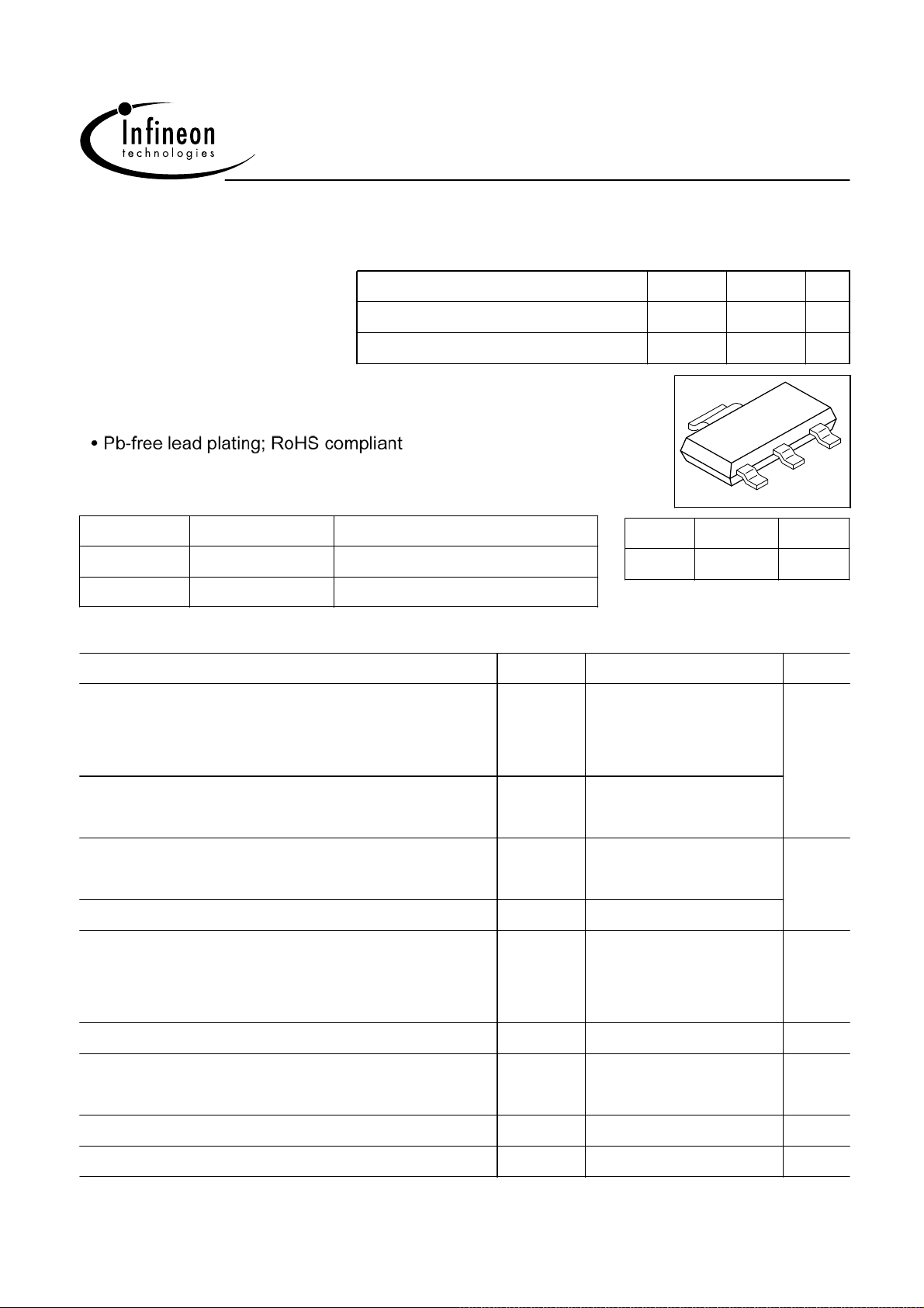
P-SOT-223
PG-SOT-223
Maximum Ratings,at
Parameter
Product Summary
Drain source voltage V
Drain-Source on-state resistance
Continuous drain current A
Tape and Reel Information
E6327
L6327
T
= 25 °C, unless otherwise specified
j
Symbol UnitValue
I
D
V
DS
R
DS(on)
I
D
4
-60
0.8
-1.17
1
Ω
2
VPS05163
Pin 1 Pin2/4 PIN 3
G D S
AContinuous drain current
3
T
= 25 °C
A
T
= 70 °C
A
Pulsed drain current
T
= 25 °C
A
Avalanche energy, single pulse
I
= -1.17 A ,
D
V
DD
= -25 V,
R
= 25 Ω
GS
Avalanche energy, periodic limited by
I
= -1.17 A,
S
T
= 150 °C
jmax
V
= -48 V, di/dt = 200 A/µs,
DS
Gate source voltage
Power dissipation
T
= 25 °C
A
Operating and storage temperature
T
jmax
I
D puls
E
AS
E
AR
dv/d
V
GS
P
tot
T
,
j
t
T
stg
-1.17
-0.94
-4.68
24 mJ
0.18
6Reverse diode dv/dt
±20
1.8 W
-55...+150 °C
IEC climatic category; DIN IEC 68-1 55/150/56
kV/µs
V
Rev.1.3 Page 1
2005-11-23
Thermal Characteristics
Parameter Symbol UnitValues
min. max.typ.
Characteristics
BSP 315 P
Thermal resistance, junction - soldering point
R
thJS
-
25 K/W-
(Pin 4)
SMD version, device on PCB:
@ min. footprint
@ 6 cm2 cooling area
1)
Electrical Characteristics, at
T
= 25 °C, unless otherwise specified
j
R
thJA
-
-
-
-
115
70
K/W
Parameter Symbol Values Unit
min. typ. max.
Static Characteristics
Drain- source breakdown voltage
V
= 0 V,
GS
Gate threshold voltage,
I
= -160 µA
D
I
= -250 µA
D
V
GS
=
V
DS
V
(BR)DSS
V
GS(th)
-60 - V-
-1 -1.5 -2
Zero gate voltage drain current
V
V
V
DS
DS
GS
= -60 V,
= -60 V,
= -20 V,
V
V
V
= 0 V,
GS
= 0 V,
GS
= 0 V
DS
T
= 25 °C
j
T
= 125 °C
j
Drain-Source on-state resistance
V
= -4.5 V,
GS
I
= -0.89 A
D
Drain-Source on-state resistance
V
= -10 V,
GS
1
Device on 40mm*40mm*1.5mm epoxy PCB FR4 with 6cm2 (one layer, 70 µm thick) copper area for drain
connection. PCB is vertical without blown air.
Rev.1.3 Page 2
I
= -1.17 A
D
I
DSS
I
GSS
R
DS(on)
R
DS(on)
-
-
-0.1
-10
-1
-100
- -10 -100Gate-source leakage current
- 0.8 1.4
- 0.5 0.8
2005-11-23
µA
nA
Ω
Ω

BSP 315 P
Electrical Characteristics, at
T
= 25 °C, unless otherwise specified
j
Parameter Symbol Values Unit
min. typ. max.
Dynamic Characteristics
Transconductance
V
≤2*
I
*
DS
R
D
DS(on)max
,
I
= -0.89 A
D
Input capacitance
V
V
= 0 V,
GS
= 0 V,
GS
V
= -25 V, f = 1 MHz
DS
V
= -25 V, f = 1 MHz
DS
Reverse transfer capacitance
V
= 0 V,
GS
V
= -25 V, f = 1 MHz
DS
Turn-on delay time
V
R
DD
G
= 18 Ω
= -30 V,
V
= -4.5 V,
GS
I
D
= -0.89 A,
g
fs
C
iss
C
oss
C
rss
t
d(on)
0.7
- 5040Output capacitance
-
- 36 ns24
S-1.4
130 160 pF-
2117
Rise time
V
R
DD
G
= 18 Ω
= -30 V,
V
= -4.5 V,
GS
Turn-off delay time
V
R
DD
G
= 18 Ω
= -30 V,
V
= -4.5 V,
GS
Fall time
V
R
DD
G
= 18 Ω
= -30 V,
V
= -4.5 V,
GS
I
= -0.89 A,
D
I
= -0.89 A,
D
I
= -0.89 A,
D
t
r
t
d(off)
t
f
- 149
-
32 48
- 19 28
Rev.1.3 Page 3
2005-11-23
 Loading...