

INFINEON BSP129 User Manual
BSP129
SIPMOS® Small-Signal-Transistor
Features
• N-channel
• Depletion mode
Product Summary
V
DS
R
DS(on),max
I
DSS,min
• dv /dt rated
• Available with V
indicator on reel
GS(th)
• Pb-free lead plating; RoHS compliant
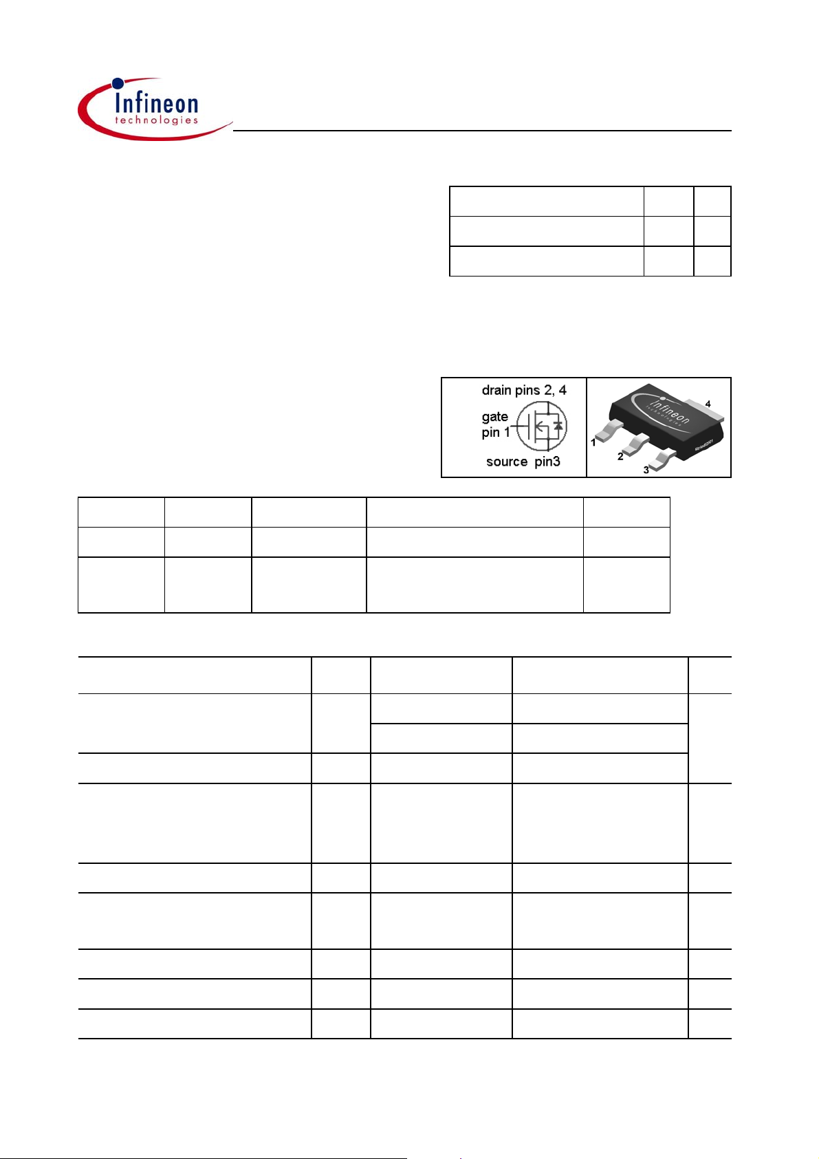
PG-SOT-223
Type Package Ordering Code Tape and Reel Information Marking
BSP129 PG-SOT- Q67000-S073 E6327: 1000 pcs/reel BSP129
240 V
6
0.05 A
Ω
BSP129 PG-SOT-
223
Maximum ratings, at T
Parameter Symbol Conditions Unit
Continuous drain current
Pulsed drain current
Reverse diode dv /dt dv /dt
Gate source voltage
ESD sensitivity (HBM) as per
MIL-STD 883
Power dissipation
Q67042 S4294 E6906: 1000 pcs/reel
sorted in V
=25 °C, unless otherwise specified
j
I
D
I
D,pulse
TA=25 °C
T
=70 °C
A
TA=25 °C
I
=0.36 A,
D
V
=192 V,
DS
di /dt =200 A/µs,
T
=150 °C
j,max
V
GS
P
tot
TA=25 °C
GS(th)
bands
1)
BSP129
Value
0.35 A
0.28
1.4
6 kV/µs
±20 V
Class 1
1.8 W
T
Operating and storage temperature
, T
j
stg
-55 ... 150 °C
IEC climatic category; DIN IEC 68-1 55/150/56
1)
see table on next page and diagram 11
Rev. 1.1 page 1 2005-02-22
BSP129
Parameter Symbol Conditions Unit
Values
min. typ. max.
Thermal characteristics
Thermal resistance,
junction - soldering point (pin 4)
SMD version, device on PCB
Electrical characteristics, at T
R
thJS
R
thJA
=25 °C, unless otherwise specified
j
minimal footprint - - 115
2
cooling area
6 cm
- - 25 K/W
1)
--70
Static characteristics
Drain-source breakdown voltage
Gate threshold voltage
Drain-source cutoff current
V
(BR)DSSVGS
V
GS(th)
I
D(off)
=-3 V, ID=250 µA
VDS=3 V, ID=108 µA
VDS=240 V,
V
=-3 V, Tj=25 °C
GS
240 - - V
-2.1 -1.4 -1
- - 0.1 µA
V
=240 V,
Gate-source leakage current
On-state drain current
Drain-source on-state resistance
Transconductance
Threshold voltage V
sorted in bands
GS(th)
J
I
I
R
g
V
GSS
DSS
DS(on)
fs
GS(th)
DS
V
=-3 V, Tj=125 °C
GS
VGS=20 V, VDS=0 V
VGS=0 V, VDS=10 V
VGS=0 V, ID=25 mA
V
=10 V, ID=0.35 A
GS
|VDS|>2|ID|R
I
=0.28 A
D
3)
VDS=3 V, ID=108 µA
DS(on)max
,
--10
- - 10 nA
50 - - mA
- 6.5 20
- 4.2 6.0
0.18 0.36 - S
-1.2 - -1 V
K -1.35 - -1.15
L -1.5 - -1.3
M -1.65 - -1.45
N -1.8 - -1.6
Ω
2)
Device on 40 mm x 40 mm x 1.5 mm epoxy PCB FR4 with 6 cm2 (single layer, 70 µm thick) copper area for
drain connection. PCB is vertical in still air.
3)
Each reel contains transistors out of one band whose identifying letter is printed on the reel label. A specific
band cannot be ordered separately.
Rev. 1.1 page 2 2005-02-22
BSP129
y
Parameter Symbol Conditions Unit
Values
min. typ. max.
namic characteristics
D
Input capacitance
Output capacitance
Reverse transfer capacitance
Turn-on delay time
Rise time
Turn-off delay time
Fall time
C
C
C
t
t
t
t
iss
oss
rss
d(on)
r
d(off)
f
V
=-3 V, VDS=25 V,
GS
f =1 MHz
V
=120 V,
DD
V
=-2...5 V,
GS
I
=0.2 A, RG=7.6 Ω
D
- 82 108 pF
-1216
-610
- 4.4 6.6 ns
- 4.1 6.2
-2233
-3553
Gate Charge Characteristics
Gate to source charge
Gate to drain charge
Gate charge total
Q
gs
Q
gd
Q
g
V
=192 V, ID=0.2 A,
DD
V
=-3 to 5 V
GS
- 0.24 0.36 nC
- 1.7 2.6
- 3.8 5.7
Gate plateau voltage
Reverse Diode
Diode continous forward current
Diode pulse current
Diode forward voltage
Reverse recovery time
Reverse recovery charge
V
plateau
I
S
I
S,pulse
V
SD
t
rr
Q
rr
=25 °C
T
A
VGS=-3 V, IF=0.35 A,
T
=25 °C
j
=120 V, IF=0.2 A,
V
R
di
/dt =100 A/µs
F
- 0.37 - V
- - 0.35 A
- - 1.4
- 0.79 1.2 V
-5380ns
-6597nC
Rev. 1.1 page 3 2005-02-22
 Loading...