

Rev. 1.11
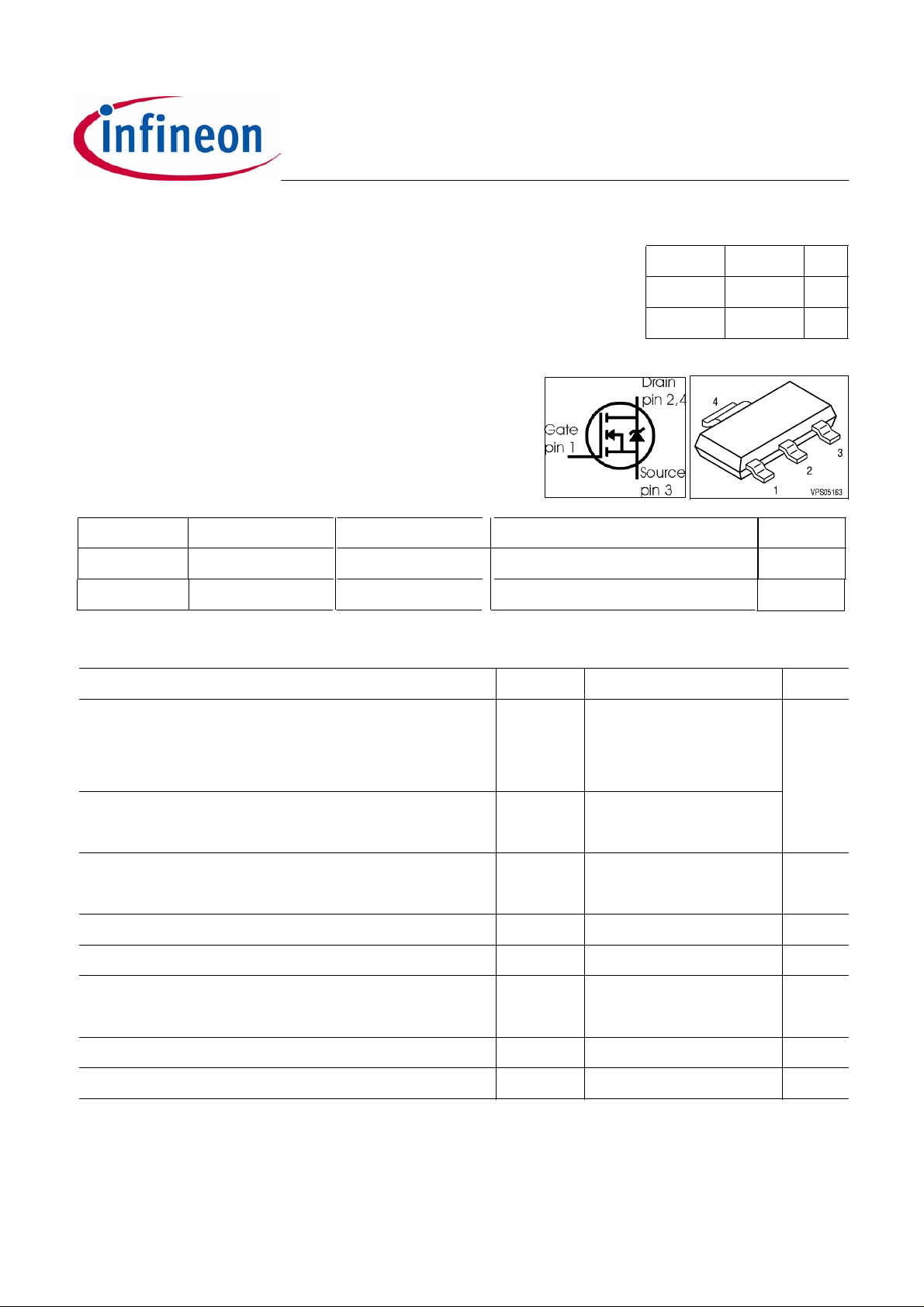
BSP125
SIPMOS Power-Transistor
Feature
• N-Channel
• Enhancement mode
• Logic Level
• dv/dt rated
Pb-free lead plating; RoHS compliant available
•
Type Package Tape and Reel Information
BSP125
BSP125
P-SOT-223
PG-SOT-223
RoHS compliant
No
Yes
E6327: 1000 pcs/reel
L6327: 1000 pcs/reel
Maximum Ratings, at Tj = 25 °C, unless otherwise specified
Product Summary
V
DS
R
DS(on)
I
D
PG-SOT-223
600 V
45 Ω
0.12 A
Marking
BSP125
BSP125
Parameter Symbol Value Unit
Continuous drain current
TA=25°C
TA=70°C
Pulsed drain current
TA=25°C
Reverse diode dv/dt
IS=0.12A, VDS=480V, di/dt=200A/µs, T
jmax
=175°C
Gate source voltage V
I
D
I
D puls
dv/dt
GS
0.12
0.1
0.48
6 kV/µs
±20
A
V
ESD Sensitivity (HBM) as per MIL-STD 883 Class 1
Power dissipation
TA=25°C, TA=25
Operating and storage temperature T
P
tot
, T
j
stg
1.8 W
-55... +150
°C
IEC climatic category; DIN IEC 68-1 55/150/56
Page 1
2006-09-28
Rev. 1.11
BSP125
Thermal Characteristics
Parameter Symbol Values Unit
min. typ. max.
Characteristics
Thermal resistance, junction - soldering point
R
thJS
- - 25 K/W
(Pin 4)
SMD version, device on PCB:
@ min. footprint
@ 6 cm2 cooling area
1)
R
thJA
-
-
-
-
115
70
Electrical Characteristics, at Tj = 25 °C, unless otherwise specified
Parameter Symbol Values Unit
min. typ. max.
Static Characteristics
Drain-source breakdown voltage
VGS=0, ID=0.25mA
Gate threshold voltage, VGS = V
ID=94µA
Zero gate voltage drain current
VDS=600V, VGS=0, Tj=25°C
DS
V
(BR)DSS
V
GS(th)
I
DSS
600 - - V
1.3 1.9 2.3
-
-
0.1
µA
VDS=600V, VGS=0, Tj=125°C
Gate-source leakage current
VGS=20V, VDS=0
Drain-source on-state resistance
VGS=4.5V, ID=0.11A
Drain-source on-state resistance
VGS=10V, ID=0.12A
1
Device on 40mm*40mm*1.5mm epoxy PCB FR4 with 6cm² (one layer, 70 µm thick) copper area for drain
connection. PCB is vertical without blown air.
Page 2
I
GSS
R
DS(on)
R
DS(on)
-
-
5
- 10 100 nA
- 26 60
Ω
- 25 45
2006-09-28
Rev. 1.11
f
BSP125
Electrical Characteristics, at Tj = 25 °C, unless otherwise specified
Parameter Symbol Conditions Values Unit
min. typ. max.
Dynamic Characteristics
Transconductance g
Input capacitance C
Output capacitance C
Reverse transfer capacitance C
Turn-on delay time t
Rise time t
Turn-off delay time t
Fall time t
Gate Charge Characteristics
Gate to source charge Q
Gate to drain charge Q
Gate charge total Q
Gate plateau voltage V
fs
iss
oss
rss
d(on)
r
d(off)
gs
gd
g
(plateau)
VDS≥2*ID*R
ID=0.1A
VGS=0, VDS=25V,
f=1MHz
DS(on)max
,
0.06 0.18 - S
- 100 150 pF
- 8.2 12.3
- 3.2 4.8
VDD=300V, VGS=10V,
ID=0.13A, RG=6Ω
- 7.7 11.6 ns
- 14.4 21
- 20 30
- 110 165
VDD=400V, ID=0.13A - 0.27 0.3 nC
- 2.3 3.5
VDD=400V, ID=0.13A,
VGS=0 to 10V
VDD=400V, ID=0.13A - 3.44 - V
- 4.4 6.6
Reverse Diode
Inverse diode continuous
I
forward current
Inv. diode direct current, pulsedI
Inverse diode forward voltage V
Reverse recovery time t
Reverse recovery charge Q
S
SM
SD
rr
rr
TA=25°C - - 0.12 A
- - 0.48
VGS=0, IF=0.12A - 0.8 1.2 V
VR=300V, I
diF/dt=100A/µs
Page 3
F=lS
,
- 156 235 ns
- 165 250 nC
2006-09-28
 Loading...