

BSO350N03
OptiMOS®2 Power-Transistor
Features
• Fast switching MOSFET for SMPS
• Optimized technology for notebook DC/DC
1
• Qualified according to JEDEC
• Dual n-channel
• Logic level
• Excellent gate charge x R
• Very low on-resistance R
• Avalanche rated
• dv /dt rated
• Pb-free lead plating; RoHS compliant
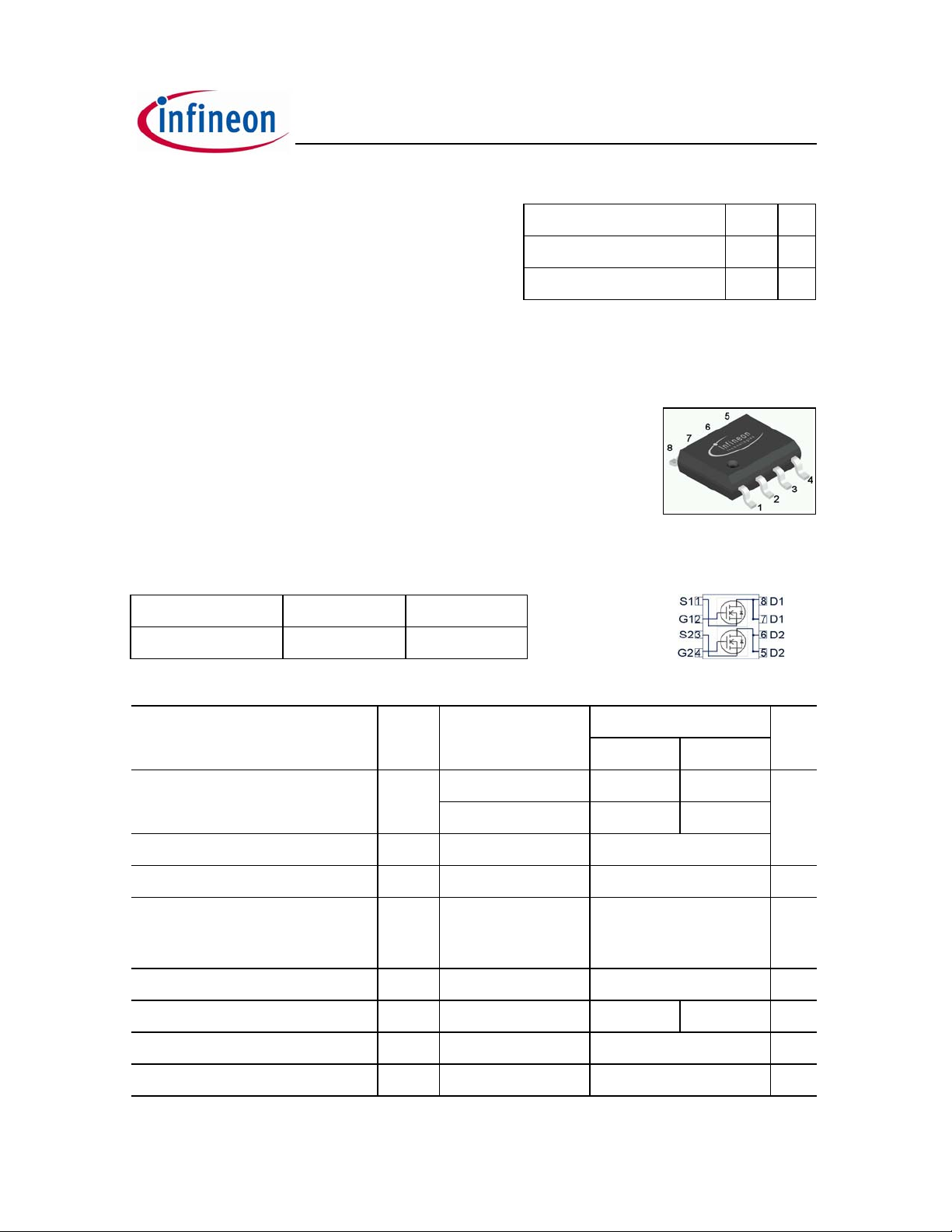
Type Package Marking
for target applications
product (FOM)
DS(on)
DS(on)
Product Summary
V
DS
R
DS(on),max
I
D
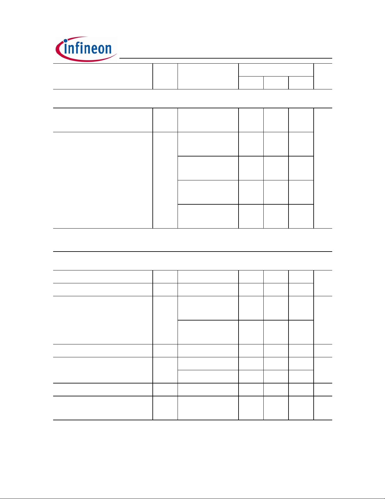
PG-DSO-8
30 V
35
6 A
mΩ
BSO350N03 PG-DSO-8 350N3
Maximum ratings, at T
Parameter Symbol Conditions Unit
=25 °C, unless otherwise specified
j
Value
10 secs steady state
=70 °C
=150 °C
2)
2)
3)
GS
2)
=25 Ω
65A
4.8 4
24
8
6
±20
mJ
kV/µs
V
2.0 1.4 W
-55 ... 150
°C
55/150/56
Continuous drain current
Pulsed drain current
Avalanche energy, single pulse
I
D
I
D,pulse
E
AS
Reverse diode dv /dt dv /dt
Gate source voltage
Power dissipation
Operating and storage temperature
V
GS
P
tot
, T
T
j
IEC climatic category; DIN IEC 68-1
TA=25 °C
T
A
TA=25 °C
ID=6 A, R
=6 A, VDS=20 V,
I
D
di /dt =200 A/µs,
T
j,max
TA=25 °C
stg
Rev. 1.5 page 1 2006-05-10
BSO350N03
Parameter Symbol Conditions Unit
Values
min. typ. max.
Thermal characteristics
Thermal resistance,
junction - soldering point
Thermal resistance,
junction - ambient
Electrical characteristics, at T
R
thJS
R
thJA
minimal footprint,
t
≤10 s
p
minimal footprint,
steady state
2
cooling area2),
6 cm
t
≤10 s
p
2
cooling area2),
6 cm
steady state
=25 °C, unless otherwise specified
j
- - 50 K/W
- - 110
- - 150
--63
--90
Static characteristics
Drain-source breakdown voltage
Gate threshold voltage
Zero gate voltage drain current
Gate-source leakage current
Drain-source on-state resistance
Gate resistance
Transconductance
1)
J-STD20 and JESD22
2)
Device on 40 mm x 40 mm x 1.5 mm epoxy PCB FR4 with 6 cm2 (one layer, 70 µm thick) copper area for drain
connection. PCB is vertical in still air.
3)
See figure 3
V
(BR)DSSVGS
V
GS(th)
I
DSS
I
GSS
R
DS(on)VGS
R
G
g
fs
=0 V, ID=1 mA
VDS=VGS, ID=6 µA
VDS=30 V, VGS=0 V,
T
=25 °C
j
V
=30 V, VGS=0 V,
DS
T
=125 °C
j
VGS=20 V, VDS=0 V
=4.5 V, ID=5 A
=10 V, ID=6 A
V
GS
|VDS|>2|ID|R
I
=6 A
D
DS(on)max
30 - - V
1.2 1.6 2
- 0.1 1 µA
- 10 100
- 10 100 nA
-4252
-2935
- 0.8 -
,
612-S
mΩ
Ω
Rev. 1.5 page 2 2006-05-10
BSO350N03
g
Parameter Symbol Conditions Unit
Values
min. typ. max.
Dynamic characteristics
Input capacitance
Output capacitance
Reverse transfer capacitance
Turn-on delay time
Rise time
Turn-off delay time
Fall time
Gate Char
e Characteristics
Gate to source charge
Gate charge at threshold
Gate to drain charge
Switching charge
4)
C
C
C
t
t
t
t
Q
Q
Q
Q
iss
oss
rss
d(on)
r
d(off)
f
gs
g(th)
gd
sw
V
=0 V, VDS=15 V,
GS
f =1 MHz
V
=15 V, VGS=10 V,
DD
=3 A, R
I
D
V
DD
V
GS
=2.7 Ω
G
=15 V, ID=3 A,
=0 to 5 V
- 360 480 pF
- 130 170
-1928
- 2.2 3.3 ns
- 2.2 3.3
- 8.7 13
- 1.4 2.1
- 1.1 1.4 nC
- 0.57 0.76
- 0.73 1.1
- 1.2 1.8
Gate charge total
Gate plateau voltage
Gate charge total, sync. FET
Output charge
Q
V
Q
Q
g
plateau
g(sync)
oss
Reverse Diode
Diode continous forward current
Diode pulse current
Diode forward voltage
Reverse recovery charge
4)
See figure 16 for gate charge parameter definition
I
S
I
S,pulse
V
SD
Q
rr
VDS=0.1 V,
V
=0 to 5 V
GS
VDD=15 V, VGS=0 V
TA=25 °C
VGS=0 V, IF=2 A,
T
=25 °C
j
VR=12 V, IF=IS,
di
/dt =400 A/µs
F
- 2.8 3.7
- 3.0 - V
- 2.4 3.2 nC
- 3.1 4.1
--2A
--24
- 0.79 1 V
--3nC
Rev. 1.5 page 3 2006-05-10
 Loading...