

g
查询BCW65供应商
NPN Silicon AF Transistor
BCW65, BCW66
For general AF applications
High current gain
Low collector-emitter saturation voltage
Complementary types: BCW67, BCW68 (PNP)
1
Type Marking Pin Configuration Package
3
BCW65A
BCW65B
BCW65C
BCW66F
BCW66G
EAs
EBs
ECs
EFs
EGs
1 = B
1 = B
1 = B
1 = B
1 = B
2 = E
2 = E
2 = E
2 = E
2 = E
3 = C
3 = C
3 = C
3 = C
3 = C
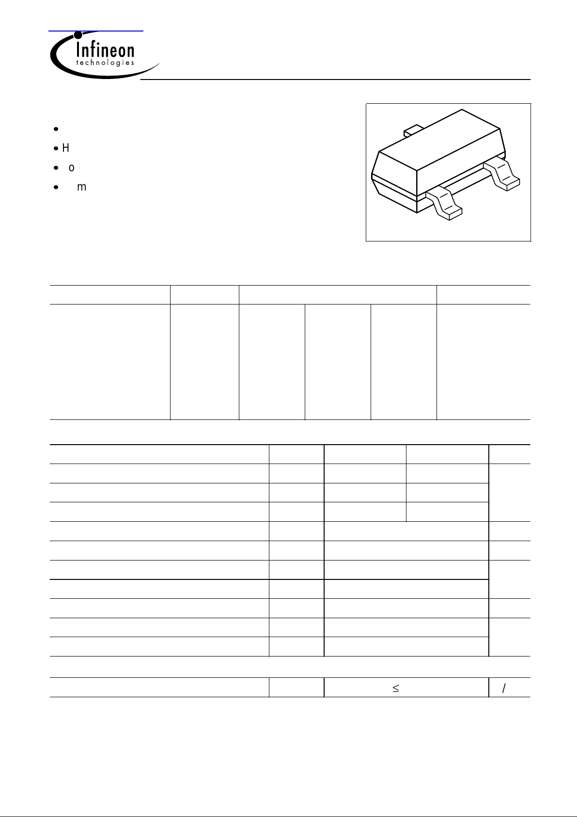
SOT23
SOT23
SOT23
SOT23
SOT23
2
VPS05161
BCW66H
EHs
1 = B
2 = E
3 = C
Maximum Ratings
Parameter
Collector-emitter voltage
Collector-base voltage
Emitter-base voltage
DC collector current
Peak collector current
Base current mA100
Peak base current
Total power dissipation, T
= 79 °C P
S
Junction temperature
Storage temperature
Symbol
V
CEO
V
CBO
V
EBO
I
C
I
CM
I
B
I
BM
tot
T
j
T
st
BCW65 BCW66
32 45 V
60 75
5 5
800 mA
1 A
200
330 mW
150 °C
-65 ... 150
Thermal Resistance
Junction - soldering point
1)
R
thJS
215 K/W
SOT23
Unit
1
For calculation of R
please refer to Application Note Thermal Resistance
thJA
1 Jul-10-2001
Electrical Characteristics at TA = 25°C, unless otherwise specified.
BCW65, BCW66
Parameter
DC Characteristics
Collector-emitter breakdown voltage
= 10 mA, IB = 0
I
C
Collector-base breakdown voltage
= 10 µA, IB = 0
I
C
Emitter-base breakdown voltage
= 10 µA, IC = 0
I
E
Collector cutoff current
= 32 V, IE = 0
V
CB
= 45 V, IE = 0
V
CB
Collector cutoff current
= 32 V, IE = 0 , TA = 150 °C
V
CB
= 45 V, IE = 0 , TA = 150 °C
V
CB
BCW65
BCW66
BCW65
BCW66
BCW65
BCW66
BCW65
BCW66
Symbol Values Unit
min. typ. max.
V
(BR)CEO
V
(BR)CBO
V
(BR)EBO
I
CBO
I
CBO
32
45
60
75
5 - -
-
-
-
-
-
-
-
-
-
-
-
-
-
-
-
-
20
20
20
20
V
nA
µA
Emitter cutoff current
= 4 V, IC = 0
V
EB
DC current gain 1)
= 100 µA, VCE = 10 V
I
C
DC current gain 1)
= 10 mA, VCE = 1 V
I
C
DC current gain 1)
= 100 mA, VCE = 1 V
I
C
h
FE
h
FE
h
FE
h
FE
h
FE
h
FE
h
FE
h
FE
h
FE
-grp.A/F
-grp.B/G
-grp.C/H
-grp.A/F
-grp.B/G
-grp.C/H
-grp.A/F
-grp.B/G
-grp.C/H
I
EBO
h
FE
h
FE
h
FE
- - 20 nA
35
50
80
75
110
180
100
160
250
-
-
-
-
-
-
160
250
350
-
-
-
-
-
-
250
400
630
-
1) Pulse test: t ≤ 300µs, D = 2%
2 Jul-10-2001

Electrical Characteristics at TA = 25°C, unless otherwise specified.
BCW65, BCW66
Parameter
DC Characteristics
DC current gain 1)
= 500 mA, VCE = 2 V
I
C
Collector-emitter saturation voltage1)
I
= 100 mA, IB = 10 mA
C
= 500 mA, IB = 50 mA
I
C
Base-emitter saturation voltage 1)
= 100 mA, IB = 10 mA
I
C
= 500 mA, IB = 50 mA
I
C
AC Characteristics
Transition frequency
= 50 mA, VCE = 5 V, f = 20 MHz
I
C
h
FE
h
FE
h
FE
-grp.A/F
-grp.B/G
-grp.C/H
Symbol Values Unit
min. typ. max.
h
FE
V
CEsat
V
BEsat
f
T
-
-
-
-
-
-
-
- 170 - MHz
35
60
100
-
-
-
-
-
-
-
0.3
0.7
1.25
2
-
V
Collector-base capacitance
= 10 V, f = 1 MHz
V
CB
Emitter-base capacitance
= 0.5 V, f = 1 MHz
V
EB
C
C
cb
eb
- 6 - pF
- 60 -
3 Jul-10-2001
BCW65, BCW66
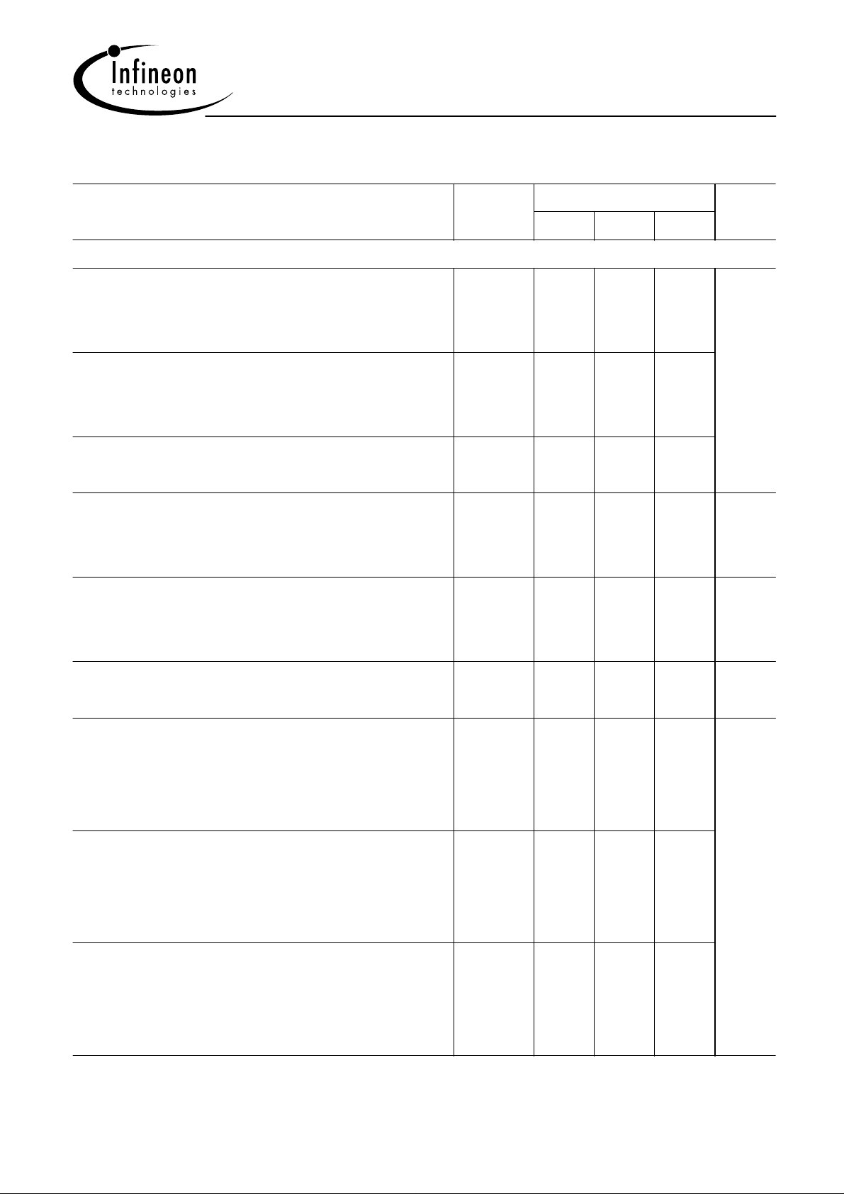
Total power dissipation P
360
mW
300
270
240
tot
P
210
180
150
120
90
60
30
0
0 15 30 45 60 75 90 105 120
= f(TS)
tot
°C
T
Transition frequency f
V
= 5V
CE
3
10
= f (IC)
T
EHP00391BCW 65/66
MHz
f
T
5
2
10
5
1
10
150
S
03
10
10
1
10
2
Ι
10mA
C
Permissible pulse load
P
totmax
P
totmax
totPDC
10
10
10
10
/ P
3
5
2
5
1
5
0
10
= f (tp)
totDC
=
D
-6
10-510-410-310
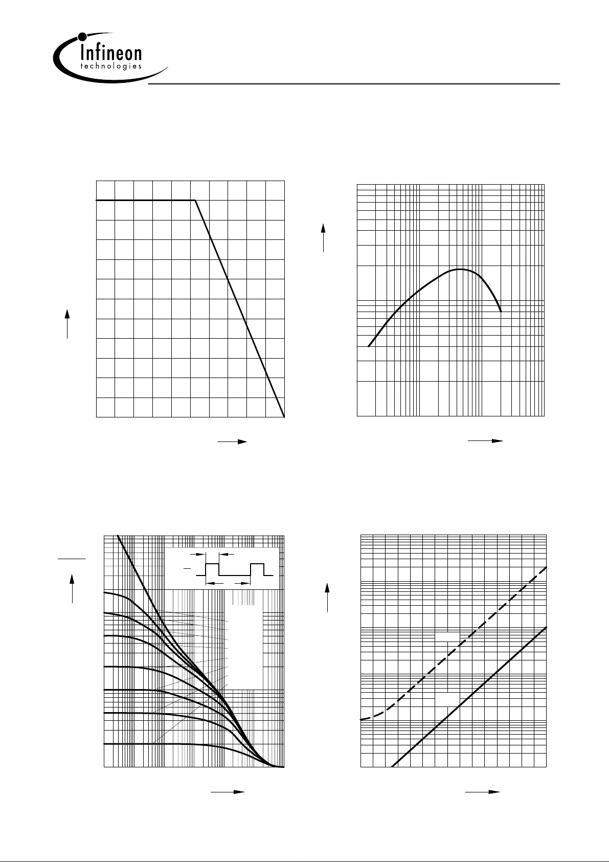
Collector cutoff current I
V
= V
CB
EHP00392BCW 65/66
t
p
t
p
T
T
Ι
CB0
CEmax
BCW 65/66 EHP00393
5
10
nA
4
10
CBO
= f (TA)
5
D
=
0
0.005
0.01
0.02
10
3
5
max
0.05
0.1
0.2
0.5
10
2
5
typ
1
10
5
0
-2
s
t
p
10
0
10
0 50 100 150
˚C
T
A
4 Jul-10-2001
BCW65, BCW66
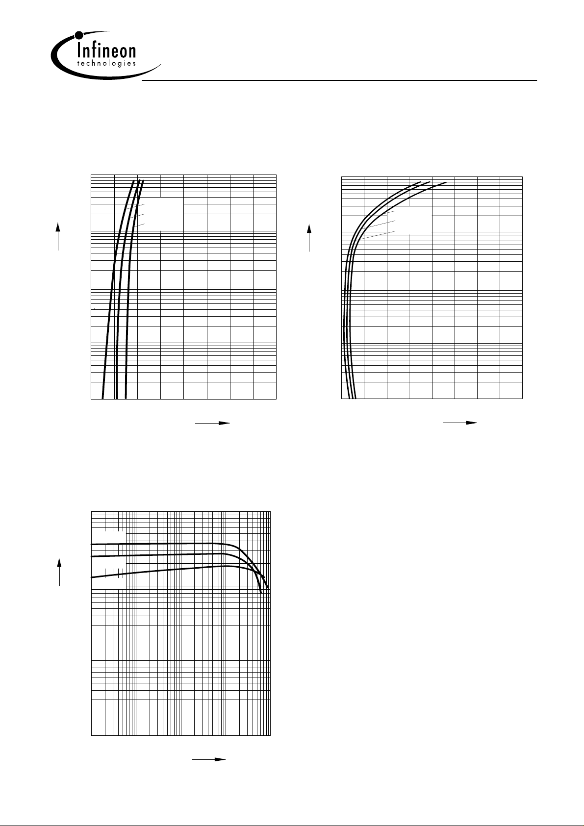
Base-emitter saturation voltage
I
= f (V
C
Ι
C
BCW 65/66 EHP00394
3
10
mA
2
10
5
1
10
5
0
10
5
-1
10
03
BEsat
), hFE = 10
150
˚C
25
˚C
-50
˚C
12 4
V
V
BE sat
Collector-emitter saturation voltage
I
= f (V
C
Ι
C
BCW 65/66 EHP00395
3
10
mA
2
10
5
1
10
5
0
10
5
-1
10
0 600
CEsat
), hFE = 10
150
˚C
25
˚C
-50
˚C
200 400 800
V
mV
CE sat
DC current gain h
V
= 1V
CE
BCW 65/66 EHP00396
3
10
5
100
˚C
h
FE
25
˚C
2
-50
10
5
1
10
5
0
10
10 10 10 10
˚C
-1 0 2 3
555
= f (IC)
FE
10
1
mA
Ι
C
5 Jul-10-2001
 Loading...