

查询BCW61A供应商
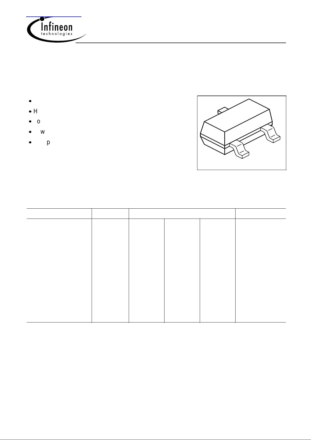
PNP Silicon AF Transistor
For AF input stages and driver applications
High current gain
Low collector-emitter saturation voltage
Low noise between 30 Hz and 15 kHz
Complementary types: BCW60, BCX70 (NPN)
BCW61, BCX71
3
1
2
VPS05161
Type Marking Pin Configuration Package
BCW 61A
BCW 61B
BCW 61C
BCW 61D
BCW 61FF
BCW 61FN
BCX 71G
BCX 71H
BCX 71J
BCX 71K
BAs
BBs
BCs
BDs
BFs
BNs
BGs
BHs
BJs
BKs
1 = B
1 = B
1 = B
1 = B
1 = B
1 = B
1 = B
1 = B
1 = B
1 = B
2 = E
2 = E
2 = E
2 = E
2 = E
2 = E
2 = E
2 = E
2 = E
2 = E
3 = C
3 = C
3 = C
3 = C
3 = C
3 = C
3 = C
3 = C
3 = C
3 = C
SOT23
SOT23
SOT23
SOT23
SOT23
SOT23
SOT23
SOT23
SOT23
SOT23
1 Jul-10-2001
Maximum Ratings
g
BCW61, BCX71
Parameter
Collector-emitter voltage
Collector-base voltage
Emitter-base voltage
DC collector current
Peak collector current 200 mA
Peak base current 200
Total power dissipation, TS = 71 °C P
Junction temperature
Storage temperature
Symbol
V
CEO
V
CBO
V
EBO
I
C
I
CM
I
BM
tot
T
j
T
st
BCW61 BCW61FF BCX71
32 32 45 V
32 32 45
5 5 5
150 °C
-65 ... 150
Unit
mA100
mW330
Thermal Resistance
Junction - soldering point
1)
R
thJS
240 K/W
Electrical Characteristics at TA = 25°C, unless otherwise specified.
Parameter
Symbol Values Unit
min. typ. max.
DC Characteristics
Collector-emitter breakdown voltage
I
= 10 mA, IB = 0
C
Collector-base breakdown voltage
I
= 10 µA, IB = 0
C
BCW61/61FF
BCX71
BCW61/61FF
BCX71
Emitter-base breakdown voltage
I
= 1 µA, IC = 0
E
1
For calculation of
R
please refer to Application Note Thermal Resistance
thJA
V
(BR)CEO
V
(BR)CBO
V
(BR)EBO
32
45
32
45
-
-
-
-
5 - -
V
-
-
-
-
2 Jul-10-2001

Electrical Characteristics at TA = 25°C, unless otherwise specified.
BCW61, BCX71
Parameter
AC Characteristics
Collector cutoff current
= 32 V, IE = 0
V
CB
= 45 V, IE = 0
V
CB
Collector cutoff current
= 32 V, IE = 0 , TA = 150 °C
V
CB
= 45 V, IE = 0 , TA = 150 °C
V
CB
Emitter cutoff current
V
= 4 V, IC = 0
EB
DC current gain 1)
= 10 µA, VCE = 5 V
I
C
BCW61/61FF
BCX71
BCW61/61FF
BCX71
hFE-grp. A/G
h
-grp. B/H
FE
h
-grp. C/J/FF
FE
h
-grp. D/K/FN
FE
Symbol Values Unit
min. typ. max.
I
CBO
I
CBO
I
EBO
h
FE
-
-
-
-
- - 20 nA
20
30
40
100
-
-
-
-
140
200
300
460
20
20
20
20
-
-
-
-
nA
µA
-
DC current gain 1)
= 2 mA, VCE = 5 V
I
C
DC current gain 1)
= 50 mA, VCE = 1 V
I
C
hFE-grp. A/G
h
-grp. B/H
FE
h
-grp. C/J/FF
FE
h
-grp. D/K/FN
FE
hFE-grp. A/G
h
-grp. B/H
FE
h
-grp. C/J/FF
FE
h
-grp. D/K/FN
FE
h
FE
120
180
250
380
h
FE
60
80
100
110
170
250
350
500
-
-
-
-
220
310
460
630
-
-
-
-
1) Pulse test: t ≤=300µs, D = 2%
3 Jul-10-2001

Electrical Characteristics at TA = 25°C, unless otherwise specified.
BCW61, BCX71
Parameter
Characteristics
Collector-emitter saturation voltage1)
I
= 10 mA, IB = 0.25 mA
C
= 50 mA, IB = 1.25 mA
I
C
Base-emitter saturation voltage 1)
= 10 mA, IB = 0.25 mA
I
C
= 50 mA, IB = 1.25 mA
I
C
Base-emitter voltage 1)
= 10 µA, VCE = 5 V
I
C
I
= 2 mA, VCE = 5 V
C
= 50 mA, VCE = 1 V
I
C
AC Characteristics
Transition frequency
I
= 20 mA, VCE = 5 V, f = 100 MHz
C
Symbol Values Unit
min. typ. max.
V
CEsat
V
BEsat
V
BE(ON)
f
T
-
-
-
-
-
0.55
-
- 250 - MHz
0.12
0.2
0.7
0.83
0.52
0.65
0.78
0.25
0.55
0.85
1.05
-
0.75
-
V
Collector-base capacitance
V
= 10 V, f = 1 MHz
CB
Emitter-base capacitance
V
= 0.5 V, f = 1 MHz
EB
Short-circuit input impedance
I
= 2 mA, VCE = 5 V, f = 1 kHz
C
Open-circuit reverse voltage transf.ratio
I
= 2 mA, VCE = 5 V, f = 1 kHz
C
hFE-grp.
A/G
B/H
C/J/FF
D/K/FN
hFE-grp.
A/G
B/H
C/J/FF
D/K/FN
C
C
h
h
cb
eb
11e
12e
- 3 - pF
- 8 -
-
-
-
-
-
-
-
-
2.7
3.6
4.5
7.5
1.5
2
2
3
k
-
-
-
-
10
-
-
-
-
-4
1) Pulse test: t ≤=300µs, D = 2%
4 Jul-10-2001

BCW61, BCX71
Electrical Characteristics at
T
= 25°C, unless otherwise specified.
A
Parameter
AC Characteristics
Short-circuit forward current transf.ratio
I
= 2 mA, VCE = 5 V, f = 1 kHz
C
Open-circuit output admittance
I
= 2 mA, VCE = 5 V, f = 1 kHz
C
Noise figure
hFE-grp.
A/G
B/H
C/J/FF
D/K/FN
hFE-grp.
A/G
B/H
C/J/FF
D/K/FN
hFE-grp.
Symbol Values Unit
min. typ. max.
h
h
F
21e
22e
-
-
-
-
-
-
-
-
200
260
330
520
18
24
30
50
-
-
-
-
-
S
-
-
-
dB
I
= 200 µA, VCE = 5 V, RS = 1 k,
C
f = 1 kHz, f = 200 Hz
Equivalent noise voltage
I
= 200 µA, VCE = 5 V, RS = 2 k,
C
f = 10 ... 50 Hz
A/K
FF/FN
hFE-grp.
FF/FN
V
-
-
n
- - 0.11 µV
2
1
-
2
5 Jul-10-2001

BCW61, BCX71
)
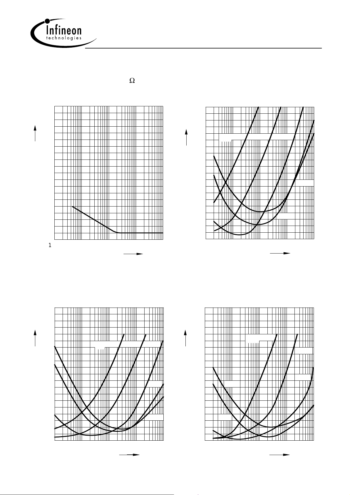
Total power dissipation P
360
mW
300
270
240
tot
P
210
180
150
120
90
60
30
0
0 15 30 45 60 75 90 105 120
= f(TS)
tot
°C
T
Collector-base capacitance
Emitter-base capacitance CEB = f (V
12
C
CBO
pF
)(
C
EBO
C
CB
= f (V
EBO
EHP00344BCW 61/BCX 71
CBO
)
10
8
C
EBO
6
4
C
CBO
2
0
150
S
-1 1
10
0
VV
CBO
EBO
10V10
)(
Permissible pulse load
P
totmax
P
totmax
totPDC
10
10
10
10
/ P
5
5
5
= f (tp)
totDC
3
2
1
0
-6
10
10-510-410-310
=
D
Transition frequency fT = f (IC)
V
= 5V
CE
EHP00345BCW 61/BCX 71
t
p
t
p
T
T
D
=
3
10
MHz
f
T
5
0
0.005
0.01
0.02
0.05
10
2
0.1
0.2
5
1
10
03
10
1
10
55
10
-2
0.5
0
10
s
t
p
EHP00347BCW 61/BCX 71
2
10mA
Ι
C
6 Jul-10-2001

BCW61, BCX71
Base-emitter saturation voltage
I
= f (V
C
Ι
C
10
mA
10
10
10
2
1
5
0
5
-1
0
), hFE = 40
BEsat
100
˚C
˚C
25
-50
˚C
0.2 0.4 0.8
0.6 V 1.2
V
EHP00348BCW 61/BCX 71
BE sat
Collector-emitter saturation voltage
I
= f (V
C
Ι
C
10
mA
10
5
10
5
10
2
1
0
-1
0
), hFE = 40
CEsat
100
25
-50
0.1 0.2 0.3 0.4
˚C
˚C
˚C
V
EHP00349BCW 61/BCX 71
CEsat
V 0.5
Collector current IC = f (VBE)
V
= 5V
CE
2
10
Ι
mA
C
1
10
5
0
10
5
100 25 -50
10
10
-1
5
-2
0
˚C
0.5 V 1.0
EHP00350BCW 61/BCX 71
˚C ˚C
V
BE
DC current gain hFE = f (IC)
V
= 5V
CE
3
10
5
100
h
FE
10
5
10
5
10
˚C
25
˚C
-50
˚C
2
1
0
-2 2
10
10
-1
10
0
10
EHP00351BCW 61/BCX 71
1
10mA
Ι
C
7 Jul-10-2001

BCW61, BCX71
Collector cutoff current I
V
= V
Ι
CB
CBO
10
10
nA
10
10
10
10
CEmax
4
3
2
1
0
-1
0
max
typ
50 100
CBO
= f (TA)
EHP00352BCW 61/BCX 71
C
T
A
150
h parameter
V
= 5V
CE
2
10
h
e
h
11e
1
10
5
h
12e
0
10
5
h
21e
-1
10
-1 1
10
h
= f (IC) normalized
e
V
CE
h
22e
0
10
5
= 5 V
EHP00353BCW 61/BCX 71
10mA
Ι
C
h parameter he = f (VCE) normalized
I
= 2mA
C
2.0
h
e
Ι
= 2 mA
C
1.5
1.0
0.5
0
0
10 20
EHP00354BCW 61/BCX 71
h
h
h
V
V
CE
Noise figure F = f (VCE)
I
= 0.2mA, RS = 2k, f = 1kHz
C
20
dB
F
11
15
10
12
22
5
30
0
-1 2
10
10
0
10
EHP00355BCW 61/BCX 71
1
10V
V
CE
8 Jul-10-2001
BCW61, BCX71
Noise figure F = f (f)
I
= 0.2mA, VCE = 5V, RS = 2k
C
20
F
dB
15
10
5
0
-2 2
10
10
-1
10
0
10
Noise figure
V
= 5V, f = 120Hz
CE
EHP00356BCW 61/BCX 71
20
dB
F
15
F = f (I
R
= 1 M
S
)
C
EHP00357BCW 61/BCX 71
Ω
100 k
Ω
10 k
Ω
10
Ω
500
5
Ω
1 k
0
1
10kHz
-3 1
10
f
10
-2
10
-1
10
0
10mA
Ι
C
Noise figure F = f (IC)
V
= 5V, f = 1kHz
CE
20
dB
F
15
10
5
0
-3 1
10
10
R
-2
= 1 M
S
10
Ω
-1
EHP00358BCW 61/BCX 71
100 kΩ10 k
500
0
10
Ι
C
1k
Noise figure F = f (IC)
V
= 5V, f = 10kHz
CE
10
0
EHP00359BCW 61/BCX 71
100 k
10 k
Ι
C
Ω
Ω
10mA
20
dB
F
Ω
= 1 M
R
Ω
15
S
10
Ω
500
Ω
5
Ω
Ω
0
10mA
10
1 k
-3 1
10
-2
10
-1
9 Jul-10-2001
 Loading...