

Page 1
PCISA -9652 Half-Size CPU Card
PCISA-9652 Half-size CPU Card
Page i
Page 2
PCISA-9652 Half-Size CPU Card
Revision
Date Version Changes
2008-04 1.00 Initial Release
Page ii
Page 3

PCISA -9652 Half-Size CPU Card
COPYRIGHT NOTICE
The information in this document is subject to change without prior notice in order to
improve reliability, design and function and does not represent a commitment on the part
of the manufacturer.
In no event will the manufacturer be liable for direct, indirect, special, incidental, or
consequential damages arising out of the use or inability to use the product or
documentation, even if advised of the possibility of such damages.
Copyright
This document contains proprietary information protected by copyright. All rights are
reserved. No part of this manual may be reproduced by any mechanical, electronic, or
other means in any form without prior written permission of the manufacturer.
TRADEMARKS
All registered trademarks and product names mentioned herein are used for identification
purposes only and may be trademarks and/or registered trademarks of their respective
owners.
Page iii
Page 4
PCISA-9652 Half-Size CPU Card
Manual Conventions
WARNING!
Warnings appear where overlooked details may cause damage to the equipment or result
in personal injury. Warnings should be taken seriously. Warnings are easy to recognize.
The word “warning” is written as “WARNING,” both capitalized and bold and is followed by
text. The text is the warning message. A warning message is shown below:
WARNING:
This is an example of a warning message. Failure to adhere to warning
messages may result in permanent damage to the PCISA-9652 or
personal injury to the user. Please take warning messages seriously.
CAUTION!
Cautionary messages should also be heeded to help reduce the chance of losing data or
damaging the PCISA-9652. Cautions are easy to recognize. The word “caution” is written
as “CAUTION,” both capitalized and bold and is followed. The italicized text is the
cautionary message. A caution message is shown below:
Page iv
Page 5
PCISA -9652 Half-Size CPU Card
CAUTION:
This is an example of a caution message. Failure to adhere to cautions
messages may result in permanent damage to the PCISA-9652.
Please take caution messages seriously.
NOTE:
These messages inform the reader of essential but non-critical information. These
messages should be read carefully as any directions or instructions contained therein can
help avoid making mistakes. Notes are easy to recognize. The word “note” is written as
“NOTE,” both capitalized and bold and is followed by text. The text is the cautionary
message. A note message is shown below:
NOTE:
This is an example of a note message. Notes should always be read.
Notes contain critical information about the PCISA-9652. Please take
note messages seriously.
Page v
Page 6
PCISA-9652 Half-Size CPU Card
Packing List
NOTE:
If any of the components listed in the checklist below are missing,
please do not proceed with the installation. Contact the IEI reseller or
vendor you purchased the PCISA-9652 from or contact an IEI sales
representative directly. To contact an IEI sales representative, please
send an email to
The items listed below should all be included in the PCISA-9652 package.
1 x PCISA-9652 CPU card
1 x IDE flat cable
1 x Mini jumper pack
1 x Parallel port and RS-232 cable
2 x SATA cables
1 x SATA power cable
1 x USB cable
1 x Utility CD
1 x Quick installation guide
Images of the above items are shown in Chapter 3.
sales@iei.com.tw.
Page vi
Page 7

PCISA -9652 Half-Size CPU Card
Table of Contents
1 INTRODUCTION..................................................................................................... 1
1.1 PCISA-9652 OVERVIEW............................................................................................ 2
1.1.1 PCISA-9652 Features........................................................................................ 2
1.2 PCISA-9652 BOARD OVERVIEW ............................................................................... 3
1.2.1 PCISA-9652 Connectors.................................................................................... 4
1.2.2 Technical Specifications..................................................................................... 6
2 DETAILED SPECIFICATIONS............................................................................. 9
2.1 OVERVIEW ............................................................................................................... 10
2.2 DIMENSIONS ............................................................................................................ 10
2.2.1 Board Dimensions............................................................................................ 10
2.2.2 External Interface Panel Dimensions...............................................................11
2.3 DATA FLOW...............................................................................................................11
2.4 COMPATIBLE PROCESSORS ....................................................................................... 13
2.5 INTEL
2.5.1 Intel® GME965 Overview................................................................................ 13
2.5.2 Intel® GME965 Front Side Bus (FSB) Support .............................................. 13
2.5.3 Intel® GME965 Memory Support..................................................................... 14
2.5.4 Intel® GME965 Integrated Graphics............................................................... 15
2.5.5 Intel® GME965 Direct Management Interface (DMI)..................................... 17
2.6 INTEL
2.6.1 Intel® ICH8ME Overview................................................................................ 18
2.6.2 Intel® ICH8ME HD Audio Controller..............................................................19
®
GME965 GRAPHICS AND MEMORY CONTROLLER HUB............................... 13
2.5.4.1 Intel® GME965 Analog CRT Support....................................................... 16
2.5.4.2 Intel® GME965 LVDS Support................................................................. 16
2.5.4.3 Intel® GME965 TV Out Support .............................................................. 16
2.5.4.4 Intel® GME965 SDVO Support ................................................................ 17
®
ICH8ME I/O CONTROLLER HUB................................................................. 18
2.6.3 Intel® ICH8ME IDE Interface ......................................................................... 20
2.6.4 Intel® ICH8ME Low Pin Count (LPC) Interface............................................. 21
2.6.5 Intel® ICH8ME PCI Interface.......................................................................... 21
2.6.5.1 ITE IT8888G PCI-to-ISA Bridge.............................................................. 21
Page vii
Page 8

2.6.6 Intel® ICH8ME PCIe x1 Bus............................................................................ 23
2.6.7 Intel® ICH8ME Real Time Clock..................................................................... 23
2.6.8 Intel® ICH8ME SATA Controller..................................................................... 23
2.6.9 Intel® ICH8ME Serial Peripheral Interface (SPI) BIOS................................. 24
2.6.10 Intel® ICH8ME USB Controller .................................................................... 24
2.7 PCIE BUS COMPONENTS .......................................................................................... 24
2.7.1 PCIe Bus Overview.......................................................................................... 24
2.7.2 Intel® 82573L PCIe GbE Controller............................................................... 25
2.8 LPC BUS COMPONENTS........................................................................................... 26
2.8.1 LPC Bus Overview........................................................................................... 26
2.8.2 Super I/O chipset.............................................................................................. 26
2.8.2.1 Super I/O LPC Interface ........................................................................... 27
2.8.2.2 Super I/O 16C550 UARTs........................................................................ 27
2.8.2.3 Super I/O Enhanced Hardware Monitor................................................... 27
PCISA-9652 Half-Size CPU Card
2.8.2.4 Super I/O Fan Speed Controller................................................................ 28
2.8.2.5 Super I/O GPIO Ports ............................................................................... 28
2.8.2.6 Super I/O Infrared..................................................................................... 28
2.8.2.7 Super I/O Keyboard Controller................................................................. 28
2.8.2.8 Super I/O Parallel Port.............................................................................. 28
2.8.2.9 Super I/O Floppy Disk Drive (FDD) Controller....................................... 29
2.9 ENVIRONMENTAL AND POWER SPECIFICATIONS ....................................................... 29
2.9.1 System Monitoring........................................................................................... 29
2.9.2 Operating Temperature and Temperature Control........................................... 30
2.9.3 Power Consumption......................................................................................... 30
3 UNPACKING.......................................................................................................... 33
3.1 ANTI-STATIC PRECAUTIONS...................................................................................... 34
3.2 UNPACKING.............................................................................................................. 34
3.2.1 Unpacking Precautions.................................................................................... 34
3.3 UNPACKING CHECKLIST........................................................................................... 35
3.3.1 Package Contents............................................................................................. 35
3.3.2 Optional Items.................................................................................................. 36
4 CONNECTORS AND JUMPERS ......................................................................... 39
4.1 PERIPHERAL INTERFACE CONNECTORS .................................................................... 40
Page viii
Page 9

PCISA -9652 Half-Size CPU Card
4.1.1 PCISA-9652 Layout......................................................................................... 40
4.1.2 Peripheral Interface Connectors ..................................................................... 41
4.1.3 Rear Panel Connectors.................................................................................... 42
4.2 INTERNAL PERIPHERAL CONNECTORS...................................................................... 43
4.2.1 AT Power Connector........................................................................................ 43
4.2.2 ATX Power Supply Enable Connector............................................................. 44
4.2.3 Audio Connector .............................................................................................. 45
4.2.4 CompactFlash® Socket.................................................................................... 46
4.2.5 Digital Input/Output Connector....................................................................... 48
4.2.6 Fan Connectors................................................................................................ 49
4.2.7 Floppy Disk Connector (34-pin)...................................................................... 50
4.2.8 Flash SPI ROM Connector.............................................................................. 52
4.2.9 Front Panel Connector.................................................................................... 53
4.2.10 IDE Connector............................................................................................... 54
4.2.11 Infrared Interface Connector ......................................................................... 56
4.2.12 Keyboard/Mouse Connector.......................................................................... 57
4.2.13 LCD Backlight Connector.............................................................................. 57
4.2.14 LVDS LCD connector.................................................................................... 58
4.2.15 Parallel Port Connector ................................................................................ 60
4.2.16 SATA Drive Connectors ................................................................................. 61
4.2.17 SDVO Connector............................................................................................ 62
4.2.18 Serial Port Connector (COM 1, RS-232)....................................................... 64
4.2.19 Serial Port Connector (COM 2, RS-232/422/485) ........................................ 65
4.2.20 TV Out Connector.......................................................................................... 66
4.2.21 Internal USB Connectors............................................................................... 67
4.3 EXTERNAL INTERFACE CONNECTORS....................................................................... 69
4.3.1 CRT Connector ................................................................................................ 69
4.3.2 Ethernet Connectors ........................................................................................ 70
4.3.3 USB Connector ................................................................................................ 71
5 INSTALLATION .................................................................................................... 73
5.1 ANTI-STATIC PRECAUTIONS...................................................................................... 74
5.2 INSTALLATION CONSIDERATIONS ............................................................................. 75
5.2.1 Installation Notices.......................................................................................... 75
5.2.2 Installation Checklist....................................................................................... 76
Page ix
Page 10

5.3 CPU, CPU COOLING KIT AND DIMM INSTALLATION ............................................. 77
5.3.1 Socket P CPU Installation............................................................................... 77
5.3.2 Cooling Kit CF-479B-RS Installation.............................................................. 79
5.3.3 DIMM Installation........................................................................................... 81
5.4 JUMPER SETTINGS.................................................................................................... 83
5.4.1 CF Card Setup ................................................................................................. 84
5.4.2 Clear CMOS Jumper........................................................................................ 85
5.4.3 COM 2 Function Select Jumper....................................................................... 86
5.4.4 LVDS Voltage Selection.................................................................................... 87
5.4.5 LVDS Panel Resolution Selection.................................................................... 88
5.5 CHASSIS INSTALLATION ........................................................................................... 90
5.5.1 Airflow.............................................................................................................. 90
5.5.2 Backplane Installation..................................................................................... 90
5.5.3 CPU Card Installation..................................................................................... 91
PCISA-9652 Half-Size CPU Card
5.6 INTERNAL PERIPHERAL DEVICE CONNECTIONS........................................................ 91
5.6.1 Peripheral Device Cables................................................................................ 91
5.6.2 IDE Cable Connection..................................................................................... 92
5.6.3 SATA Drive Connection ................................................................................... 92
5.6.4 USB Cable (Dual Port) with Slot Bracket ....................................................... 94
5.6.5 7.1 Channel Audio Kit Installation (Optional)................................................ 95
5.7 EXTERNAL PERIPHERAL INTERFACE CONNECTION................................................... 97
5.7.1 LAN Connection (Single Connector)............................................................... 97
5.7.2 VGA Monitor Connection ................................................................................ 98
5.7.3 USB Device Connection (Single Connector)................................................... 99
6 AMI BIOS.............................................................................................................. 101
6.1 INTRODUCTION ...................................................................................................... 102
6.1.1 Starting Setup................................................................................................. 102
6.1.2 Using Setup.................................................................................................... 102
6.1.3 Getting Help................................................................................................... 103
6.1.4 Unable to Reboot After Configuration Changes............................................ 103
6.1.5 BIOS Menu Bar.............................................................................................. 103
6.2 MAIN ..................................................................................................................... 104
6.3 ADVANCED............................................................................................................. 105
6.3.1 CPU Configuration........................................................................................ 106
Page x
Page 11
PCISA -9652 Half-Size CPU Card
6.3.2 IDE Configuration......................................................................................... 107
6.3.2.1 IDE Master, IDE Slave........................................................................... 109
6.3.3 Floppy Configuration......................................................................................114
6.3.4 Super IO Configuration...................................................................................115
6.3.5 Hardware Health Configuration.....................................................................118
6.3.6 Remote Access Configuration........................................................................ 120
6.3.7 USB Configuration......................................................................................... 122
6.3.7.1 USB Mass Storage Device Configuration............................................... 125
6.3.8 Power Configuration ..................................................................................... 127
6.4 PCI/PNP ................................................................................................................ 128
6.5 BOOT ..................................................................................................................... 130
6.5.1 Boot Settings Configuration........................................................................... 131
6.5.2 Boot Device Priority...................................................................................... 134
6.5.3 Removable Drives.......................................................................................... 134
6.6 SECURITY............................................................................................................... 135
6.7 CHIPSET ................................................................................................................. 136
6.7.1 NorthBridge Configuration............................................................................ 137
6.7.1.1 V ideo Function Configuration ................................................................ 139
6.7.2 Southbridge Configuration ............................................................................ 140
6.8 EXIT....................................................................................................................... 141
7 SOFTWARE DRIVERS....................................................................................... 143
7.1 AVAILABLE SOFTWARE DRIVERS............................................................................ 144
7.2 DRIVER CD AUTO-RUN.......................................................................................... 144
7.3 INTEL® CHIPSET DRIVER....................................................................................... 146
7.4 INTEL® GRAPHICS MEDIA ACCELERATOR DRIVER ................................................ 150
7.5 INTEL® 82573 PCI EXPRESS GIGABIT ETHERNET CONTROLLER DRIVER ............. 155
7.6 REALTEK HD AUDIO DRIVER (ALC883) INSTALLATION ....................................... 163
7.6.1 BIOS Setup..................................................................................................... 163
7.6.2 Driver Installation ......................................................................................... 163
7.7 INTEL
®
MATRIX STORAGE MANAGER DRIVER INSTALLATION ............................... 169
A BIOS CONFIGURATION OPTIONS ............................................................. 177
A.1 BIOS CONFIGURATION OPTIONS........................................................................... 178
B TERMINOLOGY................................................................................................. 181
Page xi
Page 12

C DIO INTERFACE................................................................................................. 187
C.1 DIO INTERFACE INTRODUCTION ........................................................................... 188
C.2 DIO CONNECTOR PINOUTS ................................................................................... 188
C.3 ASSEMBLY LANGUAGE SAMPLES........................................................................... 189
C.3.1 Enable the DIO Input Function..................................................................... 189
C.3.2 Enable the DIO Output Function.................................................................. 189
D WATCHDOG TIMER.......................................................................................... 191
E ADDRESS MAPPING.......................................................................................... 195
E.1 IO ADDRESS MAP.................................................................................................. 196
E.2 1ST MB MEMORY ADDRESS MAP.......................................................................... 196
E.3 IRQ MAPPING TABLE ............................................................................................ 197
E.4 DMA CHANNEL ASSIGNMENTS............................................................................. 197
F COMPATIBILITY................................................................................................ 199
PCISA-9652 Half-Size CPU Card
F.1 COMPATIBLE PROCESSORS ..................................................................................... 200
F.2 COMPATIBLE MEMORY MODULES .......................................................................... 200
G HAZARDOUS MATERIALS DISCLOSURE ................................................... 203
G.1 HAZARDOUS MATERIAL DISCLOSURE TABLE FOR IPB PRODUCTS CER TIFIED AS
ROHS COMPLIANT UNDER 2002/95/EC WITHOUT MERCURY..................................... 204
H INDEX.................................................................................................................... 207
Page xii
Page 13

PCISA -9652 Half-Size CPU Card
Figure 1-1: PCISA-9652 CPU Card...............................................................................2
Figure 1-2: PCISA-9652 Board Overview (Front Side)...............................................3
Figure 1-2: PCISA-9652 Board Overview (Solder Side).............................................4
Figure 2-1: PCISA-9652 Dimensions (mm) ...............................................................10
Figure 2-2: External Interface Panel Dimensions (mm)...........................................11
Figure 2-3: Data Flow Block Diagram........................................................................12
Figure 2-4: Front Side Bus (FSB)...............................................................................14
Figure 2-5: 240-pin DDR2 DIMM Socket....................................................................15
Figure 2-6: Integrated Graphics Interfaces...............................................................16
List of Figures
Figure 2-7: DMI Chip-to-Chip Connection.................................................................18
Figure 2-8: Audio Connector......................................................................................20
Figure 2-9: PCI-to-ISA Bridge.....................................................................................22
Figure 2-10: SATA Drive Connectors........................................................................23
Figure 2-11: Onboard USB Implementation .............................................................24
Figure 2-12: Intel® 82573L PCIe GbE Controllers....................................................25
Figure 2-13: iTE IT8712F Super I/O............................................................................26
Figure 4-1: Connector and Jumper Locations (Front Side)....................................40
Figure 4-1: Connector and Jumper Locations (Solder Side)..................................41
Figure 4-2: AT Power Connector Location...............................................................44
Figure 4-3: ATX Power Supply Enable Connector Location...................................45
Figure 4-4: Audio Connector Location......................................................................46
Figure 4-5: CF Card Socket Location........................................................................47
Figure 4-6: GPIO Connector Location.......................................................................49
Figure 4-7: Fan Connector Locations .......................................................................50
Figure 4-8: 34-pin FDD Connector Location.............................................................51
Figure 4-9: Flash SPI ROM Connector Locations....................................................52
Figure 4-10: Front Panel Connector Location..........................................................53
Page xiii
Page 14
Figure 4-11: IDE Device Connector Location...........................................................55
Figure 4-12: Infrared Connector Pinout Locations..................................................56
Figure 4-13: Keyboard Connector Location.............................................................57
Figure 4-14: LCD Backlight Connector Location.....................................................58
Figure 4-15: LVDS LCD Connector Location............................................................59
Figure 4-16: Parallel Port Connector Location.........................................................60
Figure 4-17: SATA Drive Connector Locations........................................................62
Figure 4-18: SDVO Connector Pinout Locations.....................................................63
Figure 4-19: RS-232 Connector Pinout Locations...................................................65
Figure 4-20: 14-Pin Serial Port Connector Locations..............................................66
Figure 4-21: TV Connector Pinout Locations...........................................................67
Figure 4-22: Internal USB Connector Locations......................................................68
Figure 4-23: PCISA-9652 External Interface Connectors........................................69
PCISA-9652 Half-Size CPU Card
Figure 4-24: VGA Connector......................................................................................69
Figure 4-25: RJ-45 Ethernet Connector ....................................................................71
Figure 5-1: Make sure the CPU socket retention screw is unlocked.....................78
Figure 5-2: Lock the CPU Socket Retention Screw.................................................79
Figure 5-3: IEI CF-479B-RS Cooling Kit ....................................................................79
Figure 5-4: Cooling Kit Support Bracket...................................................................80
Figure 5-5: Connect the cooling fan cable ...............................................................81
Figure 5-6: Installing a DIMM .....................................................................................82
Figure 5-7: Jumper Locations....................................................................................83
Figure 5-8: CF Card Setup Jumper Location............................................................84
Figure 5-9: Clear CMOS Jumper................................................................................86
Figure 5-10: COM 4 Function Select Jumper Location ...........................................87
Figure 5-11: LVDS Voltage Selection Jumper Pinout Locations............................88
Figure 5-12: LVDS Resolution Selection Jumper Pinout Locations......................89
Figure 5-13: IDE Cable Connection...........................................................................92
Page xiv
Figure 5-14: SATA Drive Cable Connection.............................................................93
Figure 5-15: SATA Power Drive Connection............................................................94
Figure 5-16: Dual USB Cable Connection.................................................................95
Figure 5-17: 7.1 Channel Audio Kit............................................................................96
Page 15

PCISA -9652 Half-Size CPU Card
Figure 5-18: LAN Connection.....................................................................................98
Figure 5-19: VGA Connector......................................................................................99
Figure 5-20: USB Device Connection..................................................................... 100
Figure 7-1: Introduction Screen.............................................................................. 145
Figure 7-2: Available Drivers................................................................................... 145
Figure 7-3: Intel® Chipset Driver Directory........................................................... 146
Figure 7-4: Intel® Chipset Driver Setup Icon......................................................... 147
Figure 7-5: Intel® Package Manager ...................................................................... 148
Figure 7-6: Intel® Setup Welcome Screen............................................................. 148
Figure 7-7: Intel® Chipset Driver License Agreement.......................................... 149
Figure 7-8: Readme File........................................................................................... 149
Figure 7-9: Intel® Chipset Driver Complete Installation Screen ......................... 150
Figure 7-10: Select the Operating System............................................................. 151
Figure 7-11: Intel® Driver Directory........................................................................ 151
Figure 7-12: Intel® VGA Driver Setup Icon............................................................ 152
Figure 7-13: GMA Driver Readme File.................................................................... 153
Figure 7-14: GMA Driver File Extraction................................................................ 153
Figure 7-15: GMA Driver Installation Welcome Screen........................................ 154
Figure 7-16: GMA Driver License Agreement........................................................ 154
Figure 7-17: GMA Driver Installing Notice............................................................. 155
Figure 7-18: GMA Driver Installation Complete .................................................... 155
Figure 7-19: Intel® 82573 Driver Directory Icon.................................................... 156
Figure 7-20: Intel® 82573 Operating System......................................................... 156
Figure 7-21: Select Operating System Type.......................................................... 157
Figure 7-22: Driver Directory................................................................................... 157
Figure 7-23: Intel® 82573 Driver Startup Icon....................................................... 158
Figure 7-24: Intel® 82573 License Agreement ...................................................... 159
Figure 7-25: Intel® 82573 File Location Select...................................................... 159
Figure 7-26: Intel® 82573 Installation Files Extraction......................................... 160
Figure 7-27: Intel® PRO Network Connections window....................................... 160
Figure 7-28: Intel® PRO Network Connections Welcome.................................... 161
Figure 7-29: License Agreement............................................................................. 161
Page xv
Page 16

Figure 7-30: Setup Type .......................................................................................... 162
Figure 7-31: Intel® 82573 Driver Installation Progress ........................................ 162
Figure 7-32: Select the Audio CODEC.................................................................... 164
Figure 7-33: Select the OS....................................................................................... 165
Figure 7-34: Select the OS Version ........................................................................ 165
Figure 7-35: Locate the Setup Program Icon ........................................................ 166
Figure 7-36: The InstallShield Wizard Starts......................................................... 166
Figure 7-37: Preparing Setup Screen..................................................................... 167
Figure 7-38: InstallShield Wizard Welcome Screen.............................................. 167
Figure 7-39: Audio Driver Software Configuration............................................... 168
Figure 7-40: Installation Wizard Updates the System .......................................... 168
Figure 7-41: Restart the Computer......................................................................... 169
Figure 7-42: SATA RAID Driver Installation Program........................................... 170
PCISA-9652 Half-Size CPU Card
Figure 7-43: SATA RAID Setup Program Icon....................................................... 171
Figure 7-44: InstallShield Wizard Setup Screen.................................................... 171
Figure 7-45: Matrix Storage Manager Setup Screen............................................. 172
Figure 7-46: Matrix Storage Manager Welcome Screen....................................... 172
Figure 7-47: Matrix Storage Manager Warning Screen ........................................ 173
Figure 7-48: Matrix Storage Manager License Agreement................................... 173
Figure 7-49: Matrix Storage Manager Readme File............................................... 174
Figure 7-50: Matrix Storage Manager Setup Complete ........................................ 174
Page xvi
Page 17
PCISA -9652 Half-Size CPU Card
Table 1-1: Technical Specifications ............................................................................7
Table 2-1: Supported Intel® Processors...................................................................13
Table 2-2: Supported HDD Specifications................................................................20
Table 2-3: Power Consumption .................................................................................31
Table 3-1: Package List Contents..............................................................................36
Table 3-2: Optional Items ...........................................................................................37
Table 4-1: Peripheral Interface Connectors..............................................................42
Table 4-2: Rear Panel Connectors.............................................................................43
Table 4-3: AT Power Connector Pinouts ..................................................................44
List of Tables
Table 4-4: ATX Power Supply Enable Connector Pinouts......................................45
Table 4-5: Audio Connector Pinouts.........................................................................46
Table 4-6: CF Card Socket Pinouts ...........................................................................48
Table 4-7: GPIO Connector Pinouts..........................................................................49
Table 4-8: Fan Connector Pinouts.............................................................................50
Table 4-9: 34-pin FDD Connector Pinouts................................................................52
Table 4-10: Flash SPI ROM Connector Pinouts .......................................................53
Table 4-11: Front Panel Connector Pinouts .............................................................54
Table 4-12: IDE Connector Pinouts...........................................................................56
Table 4-13: Infrared Connector Pinouts....................................................................56
Table 4-14: Keyboard Connector Pinouts ................................................................57
Table 4-15: LCD Backlight Connector Pinouts ........................................................58
Table 4-16: LVDS LCD Connector Pinouts...............................................................60
Table 4-17: Parallel Port Connector Pinouts............................................................61
Table 4-18: SATA Drive Connector Pinouts .............................................................62
Table 4-19: SDVO Connector Pinouts.......................................................................64
Table 4-20: RS-232 Connector Pinouts.....................................................................65
Table 4-21: COM 2 Pinouts.........................................................................................66
Table 4-22: TV Port Connector Pinouts ....................................................................67
Page xvii
Page 18

Table 4-23: USB3 and USB4 Pinouts.........................................................................68
Table 4-24: VGA Connector Pinouts .........................................................................70
Table 4-25: LAN1 and LAN2 Pinouts.........................................................................70
Table 4-26: RJ-45 Ethernet Connector LEDs............................................................71
Table 4-27: External USB Connector Pinouts..........................................................71
Table 5-1: Jumpers......................................................................................................83
Table 5-2: CF Card Setup Jumper Settings..............................................................84
Table 5-3: Clear CMOS Jumper Settings ..................................................................85
Table 5-4: COM 2 Function Select Jumper Settings................................................86
Table 5-5: LVDS Voltage Selection Jumper Settings ..............................................88
Table 5-6: LVDS Resolution Selection Jumper Settings.........................................89
Table 5-7: IEI Provided Cables...................................................................................91
Table 6-1: BIOS Navigation Keys............................................................................ 103
PCISA-9652 Half-Size CPU Card
Page xviii
Page 19

PCISA -9652 Half-Size CPU Card
List of BIOS Menus
Menu 1: Main ................................................................................................. 104
Menu 2: Advanced.................................................................................................... 106
Menu 3: CPU Configuration .................................................................................... 107
Menu 4: IDE Configuration...................................................................................... 108
Menu 5: IDE Master and IDE Slave Configuration ................................................ 110
Menu 6: IDE Master and IDE Slave Configuration ................................................ 114
Menu 7: Super IO Configuration............................................................................. 115
Menu 8: Hardware Health Configuration ............................................................... 119
Menu 9: Remote Access Configuration [Advanced] ............................................ 120
Menu 10: USB Configuration .................................................................................. 123
Menu 11: USB Mass Storage Device Configuration.............................................. 125
Menu 12: Power Configuration............................................................................... 127
Menu 13: PCI/PnP Configuration............................................................................ 128
Menu 14: Boot........................................................................................................... 131
Menu 15: Boot Settings Configuration................................................................... 132
Menu 16: Boot Device Priority Settings................................................................. 134
Menu 17: Removable Drives ................................................................................... 135
Menu 18: Security..................................................................................................... 136
Menu 19:Northbridge Chipset Configuration........................................................ 137
Menu 20:Southbridge Chipset Configuration ....................................................... 140
Menu 21: Exit............................................................................................................ 141
Page xix
Page 20

PCISA-9652 Half-Size CPU Card
THIS PAGE IS INTENTIONALLY LEFT BLANK
Page xx
Page 21
PCISA -9652 Half-Size CPU Card
Chapter
1
1 Introduction
Page 1
Page 22
1.1 PCISA-9652 Overview
PCISA-9652 Half-Size CPU Card
Figure 1-1: PCISA-9652 CPU Card
TM
The PCISA-9652 half-size PCISA CPU card is a Socket P Intel® Core
2 Duo (Merom
core) CPU platform. The PCISA-9652 has a maximum front side bus (FSB) frequency of
800 MHz and comes with a VGA interface and dual PCI Express (PCIe) Gigabit Ethernet
(GbE). The PCISA-9652 supports up to three, second-generation serial ATA (SATA) hard
disk drives (HDD) with maximum transfer rates of 3.0 Gbps and up to six USB 2.0 devices.
The PCISA-9652 also has a CompactFlash® card socket for additional system storage.
Multiple display support adds versatility to the system enabling system integrators and
designers increased flexibility in selecting display panel options.
1.1.1 PCISA-9652 Features
Some of the PCISA-9652 features are listed below:
Complies with RoHS
Supports Socket P Intel® Core™2 Duo processor with Merom core
Page 2
Supports a maximum FSB speed up to 800 MHz
Supports one 240-pin 2 GB (max.) 533/667 MHz DDR2 SDRAM DIMM
Dual PCIe GbE connectors
Supports three SATA II channels with transfer rates up to 3.0 Gbps
Page 23
PCISA -9652 Half-Size CPU Card
Supports six USB 2.0 devices
Supports HDTV-Out, 24-bit dual-channel LVDS and CRT
1.2 PCISA-9652 Board Overview
Figure 1-2: PCISA-9652 Board Overview (Front Side)
Page 3
Page 24
PCISA-9652 Half-Size CPU Card
Figure 1-3: PCISA-9652 Board Overview (Solder Side)
1.2.1 PCISA-9652 Connectors
The PCISA-9652 has the following connectors on-board:
1 x Audio connector
1 x AT power connector
1 x ATX enable connector
1 x CompactFlash® card slot
1 x DDR2 DIMM socket
1 x Digital I/O connector
1 x Fan connector
1 x Flash SPI ROM connector
1 x Floppy disk connector
Page 4
1 x Front panel connector
1 x IDE Interface connector
Page 25

PCISA -9652 Half-Size CPU Card
1 x Infrared interface connector
1 x Keyboard connector
1 x LCD backlight connector
1 x LVDS LCD connector
1 x Parallel port connector
1 x RS-232 serial port connector
1 x RS-232/422/485 serial port connector
3 x SATA II connectors
1 x SDVO connector
1 x TV out connector
2 x USB connectors
The PCISA-9652 has the following connectors on the board rear panel:
1 x CRT connector
2 x Ethernet connectors
2 x USB 2.0 ports
The PCISA-9652 has the following on-board jumpers:
CF card setup
Clear CMOS
COM 2 function selection
LCD voltage selection
LVDS panel resolution selection
The location of these connectors on the motherboard can be seen in Figure 1-1. These
connectors are fully described in Chapter 3.
Page 5
Page 26
1.2.2 Technical Specifications
PCISA-9652 technical specifications are listed in Table 1-1. Detailed descriptions of each
PCISA-9652 Half-Size CPU Card
specification can be found in Chapter
SPECIFICATION PCISA-9652
CPUs Supported
Chipsets
Graphics Support
Display
Socket P Intel® Core™2 Duo Merom core CPU
Northbridge: Intel® GME965
Southbridge: Intel® ICH8ME
Intel® Graphics Media Accelerator (GMA) X3100
CRT
HDTV:
2.
Up to 1080i component output
Composite output for NTSC/PAL
LVDS: Dual-channel 24-bit LVDS
Memory
One 240-pin 2 GB (max.) 533/667 MHz dual-channel DDR2
SDRAM DIMM
Super I/O
Serial ATA (SATA)
HDD Interface
USB Interfaces
Serial Ports
Keyboard/Mouse
Infrared
iTE IT8712F
Three SATA II connectors with 3.0 Gbps transfer rates
One IDE channel supports two Ultra ATA 100/66/33 devices
Six USB 2.0 devices supported (four internal and two
external)
One RS-232 (10-pin header connector)
One RS-232/422/485 (14-pin header connector)
One keyboard/mouse connector (6-pin header)
One IrDA connector through the iTE IT8712F super I/O.
Supports:
Serial Infrared (SIR)
Page 6
Page 27
PCISA -9652 Half-Size CPU Card
Amplitude Shift Keyed IR (ASKIR)
Digital I/O
Audio
Ethernet
BIOS
Power
Power Consumption
Operating Temperature
Humidity
Physical Dimensions
8-bit digital I/O, 4 input / 4 output by super I/O
Supports 7.1 channel HD audio via AC-KIT883HD audio kit
Dual Intel® 82573L PCIe GbE controllers
AMI BIOS Label
AT and ATX power
5V @ 7.72 A, +12V @ 0.139 A
(2.0 GHz Intel® Core™2 Duo T7300 with a 800 MHz FSB
and a 667 MHz 1 GB DDR2 DIMM)
Minimum: 0ºC (32°F)
Maximum: 60°C (140°F)
5%~95% non condensing
185 mm x 127.6 mm (width x length)
Weight (GW)
Table 1-1: Technical Specifications
1.0 kg
Page 7
Page 28

PCISA-9652 Half-Size CPU Card
THIS PAGE IS INTENTIONALLY LEFT BLANK
Page 8
Page 29

PCISA -9652 Half-Size CPU Card
Chapter
2
2 Detailed Specifications
Page 9
Page 30
2.1 Overview
This chapter describes the specifications and on-board features of the PCISA-9652 in
detail.
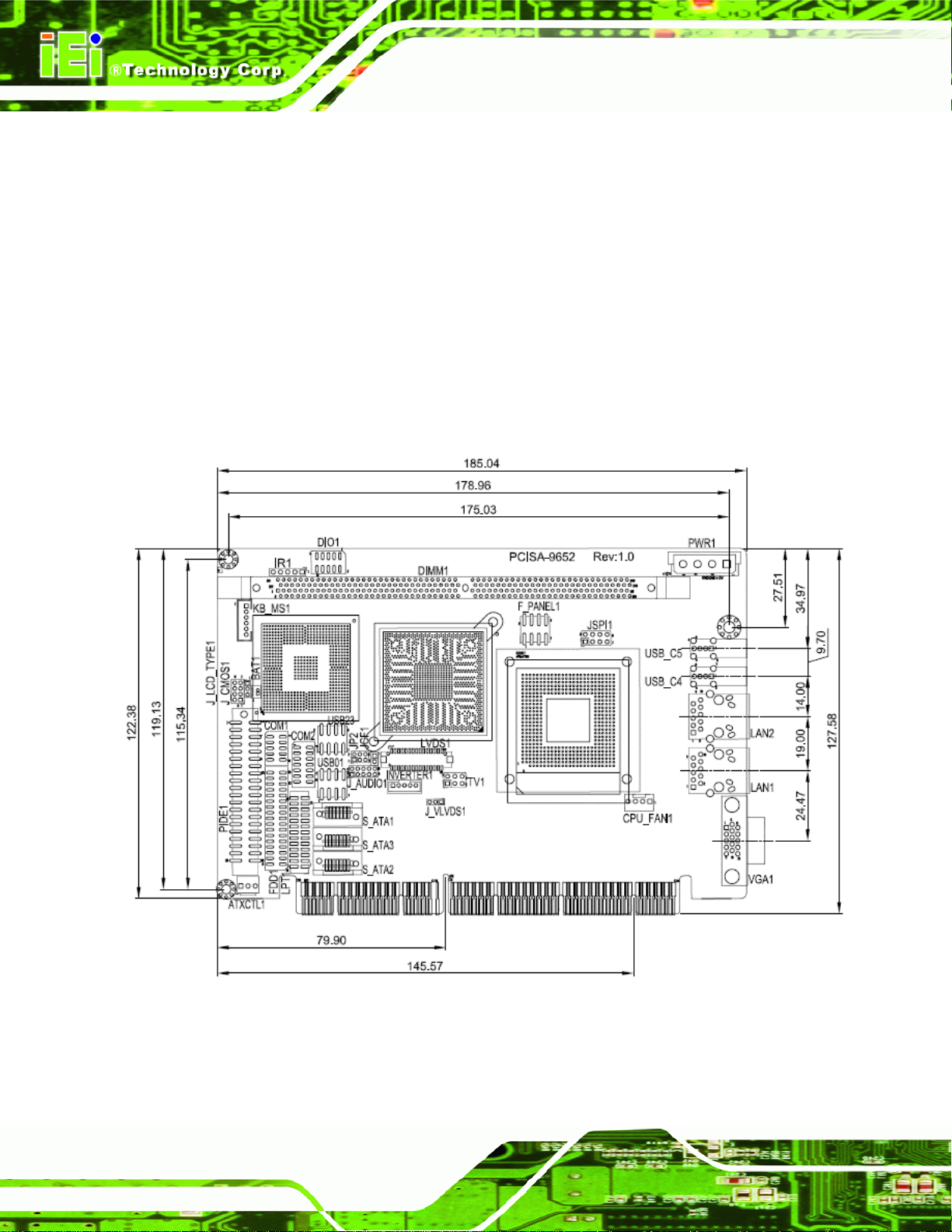
2.2 Dimensions
2.2.1 Board Dimensions
The dimensions of the board are listed below:
Length: 185.0 mm
Width: 127.6 mm
PCISA-9652 Half-Size CPU Card
Figure 2-1: PCISA-9652 Dimensions (mm)
Page 10
Page 31

PCISA -9652 Half-Size CPU Card
2.2.2 External Interface Panel Dimensions
External peripheral interface connector panel dimensions are shown in Figure 2-2.
Figure 2-2: External Interface Panel Dimensions (mm)
2.3 Data Flow
The PCISA-9652 motherboard comes with an Intel® GME965 GMCH and an Intel®
ICH8ME I/O Controller Hub.
the CPU and other components installed on the motherboard.
Figure 2-3 shows the data flow between the system chipset,
Page 11
Page 32

PCISA-9652 Half-Size CPU Card
Figure 2-3: Data Flow Block Diagram
Page 12
Page 33

PCISA -9652 Half-Size CPU Card
2.4 Compatible Processors
Table 2-1 lists the Intel® processors supported on the PCISA-9652. All the processors in
Table 2-1 are 65nm Socket P processors.
Processor Max. CPU Speed FSB Speed Max. Cache Size
Intel® Core2 Duo 2.60 GHz 800 MHz 4 MB
Intel® Celeron® M 2.13 GHz 533 MHz 1 MB
Table 2-1: Supported Intel® Processors
2.5 Intel® GME965 Graphics and Memory Controller Hub
2.5.1 Intel® GME965 Overview
The Intel® GME965 GMCH has the Intel® Graphics Media Accelerator X3100 (Intel® GMA
3100) to support integrated graphics. The integrated graphics and memory controller hub
(GMCH) facilitates the flow of information primarily between the following four interfaces:
Front Side Bus (FSB)
System Memory Interface
Graphics Interface
Direct Media Interface (DMI)
2.5.2 Intel® GME965 Front Side Bus (FSB) Support
The Intel® GME965 GMCH supports processors with the following FSB speeds:
533 MHz
800 MHz
The Socket P, Intel® GME965 GMCH and the FSB are shown in
Figure 2-4.
Page 13
Page 34

PCISA-9652 Half-Size CPU Card
Figure 2-4: Front Side Bus (FSB)
2.5.3 Intel® GME965 Memory Support
WARNING:
Only DDR2 memory module can be installed on the PCISA-9652. Do
not install DDR memory modules. If a DDR memory module is installed
on the PCISA-9652, the PCISA-9652 may be irreparably damaged.
The Intel® GME965 GMCH on the PCISA-9652 supports one 240-pin DDR2 DIMM with
the following features:
One 240-pin DIMM
DDR2 only (DO NOT install a DDR DIMM)
Single-channel
Capacities of 256 MB, 512 MB, 1 GB or 2 GB
Page 14
Transfer speeds of 533 MH z or 667 MHz
64-bit wide channel
The memory sockets are shown in
Figure 2-5.
Page 35

PCISA -9652 Half-Size CPU Card
Figure 2-5: 240-pin DDR2 DIMM Socket
2.5.4 Intel® GME965 Integrated Graphics
The Intel® GME965 GMCH has a mobile Intel® Graphics Media Accelerator X3100
integrated graphics engine that supports the following display devices:
Analog CRT
LVDS
Analog TV-Out
SDVO
Page 15
Page 36

PCISA-9652 Half-Size CPU Card
Figure 2-6: Integrated Graphics Interfaces
2.5.4.1 Intel® GME965 Analog CRT Support
A DB-15 VGA connector on the external peripheral interface connector panel is interfaced
to the Intel
an integrated 300 MHz RAMDAC and hot plug CRT support, supports analog CRT
monitors up to QXGA (2048 x 1536).
®
GME965 graphics engine. The Intel® GME965 internal graphics engine, with
2.5.4.2 Intel® GME965 LVDS Support
A 30-pin LVDS crimp connector is interfaced to the Intel® GME965 graphics engine. The
Intel® GME965 internal graphics engine supports LVDS displays with the following
features:
18-bit/24-bit 25 MHz to 112 MHz single-channel or dual-channel LVDS
screens
TFT panel type supported
Panel Fitting, Panning and Center mode supported
SPWG v3.5 specification compliant
Page 16
2.5.4.3 Intel® GME965 TV Out Support
An internal 6-pin header TV output connector is interfaced to the Intel® GME965 graphics
engine. The Intel® GME965 internal graphics engine has the following TV output feature s:
Page 37

PCISA -9652 Half-Size CPU Card
Three integrated 10-bit DACs
Overscaling
NTSC and PAL formats supported
Supports Component, S-Video, TV D connector or Composite output
connectivity
Supports with the following resolutions:
o SDTV 480i
o EDTV 480p
o HDTV 720p, 1080i
o True HDTV 1080p
2.5.4.4 Intel® GME965 SDVO Support
The Intel® GME965 internal graphics engine has the following SDVO output features:
Concurrent operation of PCIe x 1 with SDVO
One SDVO port supported
o SDVO is muxed onto the PCIe pins
o DVI 1.0 support for external digital monitor
o Only Downstream HDCP support
o Supports TV and DVD formats
o Display hot plug support
Supports multiple external SDVO components, including HDMI, DVI, LVDS,
Analog TV-out, Analog CRT.
2.5.5 Intel® GME965 Direct Management Interface (DMI)
The Direct Media Interface (DMI) is the communication bus between the Intel® GME965
GMCH and the ICH8ME I/O controller hub (ICH). The DMI is a high-speed interface that
integrates advanced priority-based servicing and allows for concurrent traffic and true
isochronous transfer capabilities. The DMI is shown in
Figure 2-7.
Page 17
Page 38

PCISA-9652 Half-Size CPU Card
Figure 2-7: DMI Chip-to-Chip Connection
®
Features of the Intel
GME965 DMI are listed below:
2GB/s (1GB/s in each direction) bus speed
Configurable as x2 or x4 DMI lanes
32-bit downstream address
2.6 Intel® ICH8ME I/O Controller Hub
2.6.1 Intel® ICH8ME Overview
The Intel® ICH8ME I/O Controller Hub (ICH) is connected to the Intel® GME965 GMCH
through the chip-to-chip Direct Media Interface (DMI). Some of the features of the Intel®
ICH8ME are listed below.
Complies with PCI Express Base Sp ecification, Revision 1.1
Complies with PCI Local Bus Specification, Revision 2.3 and supports 33
MHz PCI operations
Supports ACPI Power Management Logic
Contains:
o Enhanced DMA controller
Page 18
o Interrupt controller
o Timer functions
Integrated SATA host controller with DMA operations interfaced to three SATA
Page 39

PCISA -9652 Half-Size CPU Card
connectors on the PCISA-9652
Supports the six USB 2.0 devices on the PCISA-9652 with four UHCI
controllers and one EHCI controller
Complies with System Management Bus (SMBus) Specification, Version 2.0
Supports Intel® High Definition Audio
Contains Low Pin Count (LPC) interface
Supports Firmware Hub (FWH) interface
Serial Peripheral Interface (SPI) support
2.6.2 Intel® ICH8ME HD Audio Controller
The Intel® High Definition Audio controller integrated into the ICH8ME is connected to the
on-board audio connector. The audio connector is connected to an optional 7.1 channel
(ALC-KIT883HD) High Definition Audio codec. The audio controllers support up to six
PCM audio output channels. Complete surround sound requires six-channel audio
consisting of:
Front left
Front right
Back left
Back right
Center
Subwoofer
In addition to the basic surround sound features, the High Definition audio kit also features
multi-streaming functionality.
Page 19
Page 40

PCISA-9652 Half-Size CPU Card
Figure 2-8: Audio Connector
2.6.3 Intel® ICH8ME IDE Interface
The integrated IDE interface on the ICH8ME supports two IDE hard disks and ATAPI
devices. PIO IDE transfers up to 16 MB/s and Ultra ATA transfers of 100MB/s. The
integrated IDE interface is able to support the following IDE HDDs:
Ultra A T A/10 0, with data transfer rates up to 100 MB/s
Ultra A T A/66, with data transfer rates up to 66 MB/s
Ultra A T A/33, with data transfer rates up to 33 MB/s
Specification Ultra ATA/100 Ultra ATA/66 Ultra ATA/33
IDE devices 2 2 2
PIO Mode 0 – 4 0 – 4 0 – 4
PIO Max Transfer Rate 16.6 MB/s 16.6 MB/s 16.6 MB/s
DMA/UDMA designation
DMA/UDMA Max
Transfer
UDMA 3 - 4 UDMA 3 – 4 UDMA 2
100 MB/s 66 MB/s 33 MB/s
Controller Interface 5V 5V 5V
Table 2-2: Supported HDD Specifications
Page 20
Page 41

PCISA -9652 Half-Size CPU Card
2.6.4 Intel® ICH8ME Low Pin Count (LPC) Interface
The ICH8ME LPC interface complies with the LPC 1.1 specifications. The LPC bus from
the ICH7 is connected to the ITE IT8712F Super I/O chipset. For more detailed
information please refer to Section
2.8.2.
2.6.5 Intel® ICH8ME PCI Interface
The PCI bus on the ICH8ME is compliant with the PCI Revision 2.3 implementation. Some
of the features of the PCI interface are listed below.
PCI Revision 2.3 compliant
33 MHz
5V tolerant PCI signals (except PME#)
Integrated PCI arbiter supports up to seven PCI bus masters
2.6.5.1 ITE IT8888G PCI-to-ISA Bridge
The ICH8ME is interfaced to an ITE IT8888G PCI-to-ISA bridge through the PCI bus. The
ITE IT8888G PCI-to-ISA bridge is then connected to an ISA edge connector on the bottom
of the PCISA-9652 thereby enabling legacy ISA card expansion on the backplane. The
PCI to ISA bridge is shown in
Figure 2-9.
NOTE:
The ICH8ME integrated in PCISA-9652 supports non-DMA ISA
devices.
Page 21
Page 42

PCISA-9652 Half-Size CPU Card
Figure 2-9: PCI-to-ISA Bridge
The ITE IT8888G has a PCI specification v2.1 compliant 32-bit PCI bus interface and
supports both PCI Bus master and slave. The PCI interface supports both programmable
positive and full subtractive decoding schemes. Some of the features of the IT8888G PCI
to ISA bridge are listed below.
PCI Interface
Programmable PCI Address Decoders
PC/PCI DMA Controller
Distributed DMA Controller
ISA Interface
SM Bus
1 analog line-level mono output: MONO_OUT
Power-on Serial Bus Configuration
Serial IRQ
Versatile power-on strapping options
Supports NOGO function
Single 33 MHz Clock Input
+3.3V PCI I/F with +5V tolerant I/O buffers
Page 22
+5V ISA I/F and core Power Supply
Page 43

PCISA -9652 Half-Size CPU Card
2.6.6 Intel® ICH8ME PCIe x1 Bus
The Intel® ICH8ME GMCH has six PCIe x1 lanes. Two of the six PCIe lanes are
implemented on the PCISA-9652, including:
Two PCIe x1 lanes are connected to two Intel® 82573L GbE controllers
For more detailed information, please refer to Section
2.7.
2.6.7 Intel® ICH8ME Real Time Clock
256 bytes of battery backed RAM is provided by the Motorola MC146818A real time clock
(RTC) integrated into the ICH8ME. The RTC operates on a 3V battery and 32.768KHz
crystal. The RTC keeps track of the time and stores system data even when the system is
turned off.
2.6.8 Intel® ICH8ME SATA Controller
The integrated SATA controller on the ICH8ME supports three SATA II drives on the
PCISA-9652 with independent DMA operations. SATA controller specifications are listed
below.
Supports three SATA II drives
Supports 3.0 Gbps data transfer speeds
Supports Serial ATA S pecification, Revision 1.0a
Figure 2-10: SATA Drive Connectors
Page 23
Page 44

PCISA-9652 Half-Size CPU Card
2.6.9 Intel® ICH8ME Serial Peripheral Interface (SPI) BIOS
The 4-pin SPI is connected to an SPI BIOS chip. A licensed copy of AMI BIOS is
preinstalled on the SPI BIOS chip. A master-slave protocol is used for communication on
the SPI bus. The slave is connected to the Intel® ICH8ME and is implemented as a
tri-state bus.
2.6.10 Intel® ICH8ME USB Controller
Up to eight high-speed, full-speed or low-speed USB devices are supported by the
ICH8ME on the PCISA-9652. High-speed USB 2.0, with data transfers of up to 480MB/s,
is enabled with the ICH8ME integrated Enhanced Host Controller Interface (EHCI)
compliant host controller. USB full-speed and low-speed signaling is supported by the
ICH8ME integrated Universal Host Controller Interface (UHCI) controllers.
Six of the eight USB ports implemented on the PCISA-9652 are connected to two internal
connectors and two external connectors. See
Figure 2-11: Onboard USB Implementation
2.7 PCIe Bus Components
Figure 2-11.
2.7.1 PCIe Bus Overview
The PCIe bus is connected to components listed below:
Page 24
Page 45

PCISA -9652 Half-Size CPU Card
Two PCIe x1 lanes are connected to two Intel® PCIe GbE connectors
2.7.2 Intel® 82573L PCIe GbE Controller
Two RJ-45 Ethernet LAN connectors are interfaced directly to two Intel® 82573L PCIe
GbE controllers. The Intel® 82573L PCIe GbE controller is a compact, single-port
integrated physical layer (PHY) device with its own Memory Access Controller (MAC) and
interfaced to the Intel® ICH8ME Southbridge through a PCIe x1 lane. The Intel® 82573L
GbE controllers are shown in
Figure 2-12 below.
Figure 2-12: Intel® 82573L PCIe GbE Controllers
Some of the features of the Intel® 82573L are listed below:
2 Gbps peak bandwidth per direction
PCI Express Rev 1.0a specification
High bandwidth density per pin
Wide,pipelined internal data path architecture
Optimized transmit (Tx) and receive (Rx) queues
32 KB configurable Rx and Tx first-in/first-out (FIFO)
IEEE 802.3x*-compliant flow-control support with software controllable pause
times and threshold values
Programmable host memory Rx buffers (256 B-16 KB)
Descriptor ring management hardware for Tx and Rx
Page 25
Page 46

Mechanism for reducing interrupts from Tx/Rx operations
Integrated PHY for 10/100/1000 Mbps (full- and half-duplex)
IEEE 802.3ab* auto-negotiation support
IEEE 802.3ab PHY compliance and compatibility
Tx/Rx IP,TCP,and UDP checksum offloading
Tx TCP segmentation
IEEE 802.1q* Virtual Local Area Network (VLAN) support with VLAN tag
insertion, stripping, and packet filtering for up to 4096 VLAN tags
Boot ROM Preboot eXecution Environment (PXE) Flash interface support
SDG 3.0,WfM 3.0 and PC2001 compliant
Wake on LAN support
2.8 LPC Bus Components
2.8.1 LPC Bus Overview
PCISA-9652 Half-Size CPU Card
The LPC bus is connected to components listed below:
Super I/O chipset
2.8.2 Super I/O chipset
The iTE IT8712F Super I/O chipset is connected to the ICH8ME through the LPC bus. iTE
IT8712F Super I/O chipset is shown in
Figure 2-13 below.
Page 26
Figure 2-13: iTE IT8712F Super I/O
Page 47

PCISA -9652 Half-Size CPU Card
The iTE IT8712F is an LPC interface-based Super I/O device that comes with
Environment Controller integration. Some of the features of the iTE IT8712F chipset are
listed below:
LPC Interface
PC98/99/2001, ACPI and LANDesk Co mpliant
Enhanced Hardware Monitor
Fan Speed Controller
SmartGuardian Controller
Single +5V Power Supply
Two 16C550 UARTs for serial port control
Keyboard Controller
Watchdog T i mer
Serial IRQ Support
Vbat & Vcch Support
Single +5V Power Supply
Some of the Super I/O features are described in more detail below:
2.8.2.1 Super I/O LPC Interface
The LPC interface on the Super I/O complies with the Intel® Low Pin Count Specification
Rev. 1.0. The LPC interface supports both LDRQ# and SERIRQ protocols as well as PCI
PME# interfaces.
2.8.2.2 Super I/O 16C550 UARTs
The onboard Super I/O has two integrated 16C550 UARTs that can support the following:
Two standard serial ports (COM1 and COM2)
IrDa 1.0 and ASKIR protocols
2.8.2.3 Super I/O Enhanced Hardware Monitor
The Super I/O Enhanced Hardware Monitor monitors three thermal inputs, VBAT
internally, and eight voltage monitor inputs. These hardware parameters are reported in
the BIOS and can be read from the BIOS Hardware Health Configuration menu.
Page 27
Page 48

PCISA-9652 Half-Size CPU Card
2.8.2.4 Super I/O Fan Speed Controller
The Super I/O fan speed controller enables the system to monitor the speed of the fan.
One of the pins on the fan connector is reserved for fan speed detection and interfaced to
the fan speed controller on the Super I/O. The fan speed is then reported in the BIOS.
2.8.2.5 Super I/O GPIO Ports
The Super I/O has 38 programmable GPIO pins of which 8 are implemented on the
PCISA-9652. The GPIO connector has 8 programmable bits, 4-bit input and 4-bit output.
2.8.2.6 Super I/O Infrared
The Super I/O has dedicated infrared (IrDA) pins that are interfaced to an IrDA connector.
The IrDA connector is compatible with the following standards:
ASKIR
SIR
2.8.2.7 Super I/O Keyboard Controller
The Super I/O keyboard controller can execute the 8042 instruction set. Some of the
keyboard controller features are listed below:
The 8042 instruction is compatible with a PS/2 keyboard and PS/2 mouse
Gate A20 and Keyboard reset output
Supports multiple keyboard power on events
Supports mouse double-click and/or mouse move power on events
2.8.2.8 Super I/O Parallel Port
The Super I/O parallel port (LPT) is compatible with the following LPT specifications.
Bi-directional SPP compatible
Page 28
EPP V. 1.7 and V. 1.9 compatible
Extended Parallel Port (EPP) mode supported. Compatible with IEEE 1284
specifications
Enhanced printer port back-drive current protection
Page 49

PCISA -9652 Half-Size CPU Card
The parallel port controller is connected to an on-board LPT connector on the
PCISA-9652.
2.8.2.9 Super I/O Floppy Disk Drive (FDD) Controller
The Super I/O FDD controller is compatible with the following specifications.
FDD anti-virus functions with software write protect and FDD write enable
signal
Supports 3.5-inch or 5.25-inch FDD
Compatible with industry standard 82077
Supported capacities:
o 360K
o 720K
o 1.2M
o 1.44M
o 2.88M
Supported transfer rates
o 250Kbps
o 300Kbps
o 500Kbps
o 1Mbps
o 2Mbps
3-mode FDD drives supported
The FDD controller is interfaced to a FDD connector on the PCISA-9652.
2.9 Environmental and Power Specifications
2.9.1 System Monitoring
Three thermal inputs on the PCISA-9652 Super I/O Enhanced Hardware Monitor monitor
the following temperatures:
CPU temperature
PWM temperature
System temperature
Page 29
Page 50

PCISA-9652 Half-Size CPU Card
Eight voltage inputs on the PCISA-9652 Super I/O Enhanced Hardware Monitor monitor
the following voltages:
CPU Core
+1.8V
+3.30V
+5.00V
+12.0V
+1.05V
+1.5V
+1.25V
VBAT
The PCISA-9652 Super I/O Enhanced Hardware Monitor also monitors the following fan
speed:
CPU Fan speed
The values for the above environmental parameters are all recorded in the BIOS
Hardware Health Configuration menu.
2.9.2 Operating Temperature and Temperature Control
The maximum and minimum operating temperatures for the PCISA-9652 are listed below.
Minimum Operating Temperature: 0ºC (32°F)
Maximum Operating Temperature: 60°C (140°F)
A cooling fan and heat sink must be installed on the CPU. Thermal paste must be
smeared on the lower side of the heat sink before it is mounted on the CPU. Heat sinks
are also mounted on the GMCH and ICH chipsets to ensure the operating temperature of
these chips remain low.
2.9.3 Power Consumption
Page 30
Page 51

PCISA -9652 Half-Size CPU Card
Table 2-3 shows the power consumption parameters for the PCISA-9652 running with a
2.0GHz Intel® Core™2 Duo T7300 with a 800 MHz FSB and a 667 MHz 1 GB DDR2
DIMM,
Voltage Current
+5V 7.72 A
+12V 0.139 A
Table 2-3: Power Consumption
Page 31
Page 52

PCISA-9652 Half-Size CPU Card
THIS PAGE IS INTENTIONALLY LEFT BLANK
Page 32
Page 53

PCISA -9652 Half-Size CPU Card
Chapter
3
3 Unpacking
Page 33
Page 54

3.1 Anti-static Precautions
WARNING:
Failure to take ESD precautions during the installation of the
PCISA-9652 may result in permanent damage to the PCISA-9652 and
severe injury to the user.
Electrostatic discharge (ESD) can cause serious damage to electronic components,
including the PCISA-9652. Dry climates are especially susceptible to ESD. It is therefore
critical that whenever the PCISA-9652, or any other electrical component is handled, the
following anti-static precautions are strictly adhered to.
PCISA-9652 Half-Size CPU Card
Wear an anti-static wristband: Wearing a simple ant i-static wristband can
help to prevent ESD from damaging the board.
Self-grounding: Before handling the board touch any grounded conducting
material. During the time the board is handled, frequently touch any
conducting materials that are connected to the ground.
Use an anti-static pad: When configuring the PCISA-9652, place it on an
antic-static pad. This reduces the possibility of ESD damaging the
PCISA-9652.
Only handle the edges of the PCB: When handling the PCB, hold the PCB
by the edges.
3.2 Unpacking
3.2.1 Unpacking Precautions
When the PCISA-9652 is unpacked, please do the following:
Follow the anti-static precautions outlined in Section 3.1.
Page 34
Make sure the packing box is facing upwards so the PCISA-9652 does not fall
out of the box.
Make sure all the components shown in Section 3.3 are present.
Page 55

PCISA -9652 Half-Size CPU Card
3.3 Unpacking Checklist
NOTE:
If some of the components listed in the checklist below are missing,
please do not proceed with the installation. Contact the IEI reseller or
vendor you purchased the PCISA-9652 from or contact an IEI sales
representative directly. To contact an IEI sales representative, please
send an email to
sales@iei.com.tw.
3.3.1 Package Contents
The PCISA-9652 is shipped with the following components:
Quantity Item and Part Number Image
1 PCISA-9652 CPU card
1 Parallel port and RS-232 cable
(P/N:19800-000027-RS)
1 IDE cable
(P/N: 32200-000052-RS)
2 SATA cables
(P/N: 32000-000138-RS)
1 SATA power cable
(P/N: 32100-087100-RS)
Page 35
Page 56

1 Mini jumper pack
1 Quick Installation Guide
1 Dual port USB cable
(P/N: CB-USB02A-RS)
1 Utility CD
PCISA-9652 Half-Size CPU Card
Table 3-1: Package List Contents
3.3.2 Optional Items
NOTE:
The items listed in this section are optional items that must be ordered
separately. Please contact your PCISA-9652 vendor, distributor or
reseller for more information or, contact IEI directly by sending an email
to
sales@iei.com.tw.
The following optional items are available for the PCISA-9652.
Quantity Item and Part Number Image
Page 36
1 7.1 Channel HD audio kit with Realtek
ALC883
(P/N: AC-KIT883HD-R10)
Page 57

PCISA -9652 Half-Size CPU Card
Quantity Item and Part Number Image
1 CPU Cooler
(P/N: CF-479B-RS)
1 FDD cable
(P/N: 32200-000058-RS)
1 KB/MS cable with bracket
(P/N: 19800-000075-RS)
1 HDTV cable set with
S-Video/Composite/Component interfaces
(P/N: HDTVCABLESET-01)
1 RS-232/422/485 cable
(P/N: 32200-000077-RS)
Table 3-2: Optional Items
Page 37
Page 58

PCISA-9652 Half-Size CPU Card
THIS PAGE IS INTENTIONALLY LEFT BLANK
Page 38
Page 59

PCISA -9652 Half-Size CPU Card
Chapter
4
4 Connectors and
Jumpers
Page 39
Page 60

4.1 Peripheral Interface Connectors
Section 4.1.1 shows peripheral interface connector locations. Section 4.1.2 lists all the
PCISA-9652 Half-Size CPU Card
peripheral interface connectors seen in Section
4.1.1.
4.1.1 PCISA-9652 Layout
Figure 4-1 shows the on-board peripheral connectors, backplane peripheral connectors
and on-board jumpers.
Page 40
Figure 4-1: Connector and Jumper Locations (Front Side)
Page 61

PCISA -9652 Half-Size CPU Card
Figure 4-2: Connector and Jumper Locations (Solder Side)
4.1.2 Peripheral Interface Connectors
Table 4-1 shows a list of the peripheral interface connectors on the PCISA-9652. Detailed
descriptions of these connectors can be found in Section
Connector Type Label
AT power connector 4-pin connector PWR1
ATX enable connector 3-pin wafer ATXCTL1
Audio connector 10-pin header J_AUDIO1
CompactFlash® card slot 50-pin slot CF1
DDR2 DIMM socket 240-pin slot DIMM1
4.2.
Digital Input/Output connector 10-pin header DIO1
Fan connector, CPU 4-pin wafer connector CPU_FAN1
Page 41
Page 62

FDD connector 34-pin header FDD1
Flash SPI ROM connector 8-pin header JSPI1
Front panel connector 8-pin header F_PANEL1
IDE Interface connector 40-pin box header PIDE1
Infrared interface connector 5-pin header IR1
Keyboard connector 6-pin wafer KB_MS1
LCD backlight connector 5-pin wafer connector INVERTER1
LVDS LCD connector 30-pin crimp connector LVDS1
Parallel port connector 26-pin header LPT1
SATA drive connector (1) 7-pin SATA connector S_ATA1
PCISA-9652 Half-Size CPU Card
SATA drive connector (2) 7-pin SATA connector S_ATA2
SATA drive connector (3) 7-pin SATA connector S_ATA3
SDVO connector 47-pin connector CN1
Serial port connector 10-pin header COM1
Serial port connector 14-pin header COM2
TV out connector 6-pin header TV1
USB connector (1) 8-pin header USB01
USB connector (2) 8-pin header USB23
Table 4-1: Peripheral Interface Connectors
4.1.3 Rear Panel Connectors
Table 4-2 lists the rear panel connectors on the PCISA-9652. Detailed descriptions of
Page 42
these connectors can be found in Section
4.3.
Page 63

PCISA -9652 Half-Size CPU Card
Connector Type Label
CRT connector 15-pin female connector VGA1
Ethernet connector (1) RJ-45 connector LAN1
Ethernet connector (2) RJ-45 connector LAN2
USB 2.0 port (1) USB port connector USB_C4
USB 2.0 port (2) USB port connector USB_C5
Table 4-2: Rear Panel Connectors
4.2 Internal Peripheral Connectors
Internal peripheral connectors are found on the motherboard and are only accessible
when the motherboard is outside of the chassis. T his se ction h as complet e d esc ription s of
all the internal, peripheral connectors on the PCISA-9652.
4.2.1 AT Power Connector
CN Label: PWR1
CN Type:
CN Location: See
CN Pinouts: See
The 4-pin AT power connector is connected to an AT power supply.
4-pin connector (1x4)
Figure 4-3
Table 4-3
Page 43
Page 64

PCISA-9652 Half-Size CPU Card
Figure 4-3: AT Power Connector Location
PIN NO. DESCRIPTION
1 +12V
2 GND
3 GND
4 +5V
Table 4-3: AT Power Connector Pinouts
4.2.2 ATX Power Supply Enable Connector
CN Label: A TXCTL1
CN Type:
CN Location: See
CN Pinouts: See
The ATX power supply enable connector enables the PCISA-9652 to be connected to an
3-pin wafer (1x3)
Figure 4-4
Table 4-4
Page 44
ATX power supply.
Page 65

PCISA -9652 Half-Size CPU Card
Figure 4-4: ATX Power Supply Enable Connector Location
PIN NO. DESCRIPTION
1 GND
2 PS-ON
3 +5V Standby
Table 4-4: ATX Power Supply Enable Connector Pinouts
4.2.3 Audio Connector
CN Label: J_AUDIO1
CN Type:
CN Location: See
CN Pinouts: See
The audio connector connects to the optional audio kit to provide 7.1 channel HD audio to
the system.
10-pin header (2x5)
Figure 4-5
Table 4-5
Page 45
Page 66

PCISA-9652 Half-Size CPU Card
Figure 4-5: Audio Connector Location
PIN NO. DESCRIPTION PIN NO. DESCRIPTION
1 HDA_SYNC 2 HDA_BITCLK
3 HDA_SDOUT 4 SB_SPKR
5 HDA_SDIN0 6 HDA_RST#
7 VCC 8 GND
9 +12V 10 GND
Table 4-5: Audio Connector Pinouts
4.2.4 CompactFlash® Socket
CN Label: CF1 (solder side)
CN Type:
CN Location: See
CN Pinouts: See
A CF Type I or Type II memory card is inserted to the CF socket on the solder side of the
PCISA-9652.
50-pin slot (2x25)
Figure 4-6
Table 4-6
Page 46
Page 67

PCISA -9652 Half-Size CPU Card
Figure 4-6: CF Card Socket Location
Page 47
Page 68

PCISA-9652 Half-Size CPU Card
PIN NO. DESCRIPTION PIN NO. DESCRIPTION
1 GROUND 26 VCC-IN CHECK1
2 DATA 3 27 DATA 11
3 DATA 4 28 DATA 12
4 DATA 5 29 DATA 13
5 DATA 6 30 DATA 14
6 DATA 7 31 DATA 15
7 HDC_CS0# 32 HDC_CS1
8 N/C 33 N/C
9 GROUND 34 IOR#
10 N/C 35 IOW#
11 N/C 36 VCC_COM
12 N/C 37 IRQ15
13 VCC_COM 38 VCC_COM
14 N/C 39 CSEL
15 N/C 40 N/C
16 N/C 41 HDD_RESET
17 N/C 42 IORDY
18 SA2 43 SDREQ
19 SA1 44 SDACK#
20 SA0 45 HDD_ACTIVE#
21 DATA 0 46 66DET
22 DATA 1 47 DATA 8
23 DATA 2 48 DATA 9
24 N/C 49 DATA 10
25 VCC-IN CHECK2 50 GROUND
Table 4-6: CF Card Socket Pinouts
4.2.5 Digital Input/Output Connector
CN Label: DIO1
CN Type:
Page 48
10-pin header (2x5)
Page 69

PCISA -9652 Half-Size CPU Card
CN Location: See Figure 4-7
CN Pinouts: See
Table 4-7
The DIO connector is managed through a Super I/O chip. The DIO connector pins are
user programmable. The digital IO port of PCISA-9652 is 5V CMOS level.
Figure 4-7: GPIO Connector Location
PIN NO. DESCRIPTION PIN NO. DESCRIPTION
1 GND 2 VCC
3 OUTPUT 3 4 OUTPUT 2
5 OUTPUT 1 6 OUTPUT 0
7 INPUT 3 8 INPUT 2
9 INPUT 1 10 INPUT 0
Table 4-7: GPIO Connector Pinouts
4.2.6 Fan Connectors
CN Label: CPU_FAN1
CN Type:
CN Location: See
4-pin wafer connector (1x3)
Figure 4-8
Page 49
Page 70

PCISA-9652 Half-Size CPU Card
CN Pinouts: See Table 4-8
The cooling fan connector provides a 12V, 500mA current to a CPU cooling fan. The
connector has a "rotation" pin to get rotation signals from fans and notify the system so the
system BIOS can recognize the fan speed. Please note that only specified fans can issue
the rotation signals.
Figure 4-8: Fan Connector Locations
PIN NO. DESCRIPTION
1 GND
2 +12V
3 Rotation Signal
4 Control
Table 4-8: Fan Connector Pinouts
4.2.7 Floppy Disk Connector (34-pin)
CN Label: FDD1
CN Type:
34-pin header (2x17)
Page 50
Page 71

PCISA -9652 Half-Size CPU Card
CN Location: See Figure 4-9
CN Pinouts: See
Table 4-9
The floppy disk connector is connected to a floppy disk drive.
Figure 4-9: 34-pin FDD Connector Location
PIN NO. DESCRIPTION PIN NO. DESCRIPTION
1 GND 2 REDUCE WRITE
3 GND 4 N/C
5 N/C 6 N/C
7 GND 8 INDEX#
9 GND 10 MOTOR ENABLE A#
11 GND 12 DRIVE SELECT B#
13 GND 14 DRIVE SELECT A#
15 GND 16 MOTOR ENABLE B#
17 GND 18 DIRECTION#
19 GND 20 STEP#
21 GND 22 WRITE DATA#
23 GND 24 WRITE GATE#
25 GND 26 TRACK 0#
Page 51
Page 72

27 GND 28 WRITE PROTECT#
29 GND 30 READ DATA#
31 GND 32 SIDE 1 SELECT#
33 GND 34 DISK CHANGE#
Table 4-9: 34-pin FDD Connector Pinouts
4.2.8 Flash SPI ROM Connector
CN Label: JSPI1
PCISA-9652 Half-Size CPU Card
CN Type:
CN Location: See
CN Pinouts: See
8-pin header (2x4)
Figure 4-23
Table 4-23
Use the Flash SPI ROM connector to flash SPI ROM.
Page 52
Figure 4-10: Flash SPI ROM Connector Locations
PIN NO. DESCRIPTION PIN NO. DESCRIPTION
1 3.3V 2 GND
3 CS0 4 CLK
5 SO0 6 SI
Page 73

PCISA -9652 Half-Size CPU Card
7 NC 8 NC
Table 4-10: Flash SPI ROM Connector Pinouts
4.2.9 Front Panel Connector
CN Label: F_PANEL1
CN Type:
CN Location: See
CN Pinouts: See
8-pin header (2x4)
Figure 4-11
Table 4-11
The front panel connector connects to several external switches and indicators to monitor
and control the motherboard. These indicators and switches include:
Power LED
Power button
Reset button
HDD LED
Figure 4-11: Front Panel Connector Location
Page 53
Page 74

PCISA-9652 Half-Size CPU Card
FUNCTION PIN DESCRIPTION FUNCTION PIN DESCRIPTION
Button
1 PWR_BTN+ 2 PWR_LED+ Power
3 PWR_BTN5 HDD_LED+ 6 RESET+ HDD LED
7 HDD_LED-
Power
LED
Reset
4 PWR_LED-
8 RESET-
Table 4-11: Front Panel Connector Pinouts
4.2.10 IDE Connector
CN Label: PIDE1
CN Type:
CN Location: See
CN Pinouts: See
One primary 40-pin IDE device connector on the PCISA-9652 motherboard supports
40-pin box header (2x20)
Figure 4-12
Table 4-12
connectivity to ATA 100/66/33 IDE devices with data transfer rates up to 100MB/s.
Page 54
Page 75

PCISA -9652 Half-Size CPU Card
Figure 4-12: IDE Device Connector Location
PIN NO. DESCRIPTION PIN NO. DESCRIPTION
1 RESET# 2 GND
3 DATA 7 4 DATA 8
5 DATA 6 6 DATA 9
7 DATA 5 8 DATA 10
9 DATA 4 10 DATA 11
11 DATA 3 12 DATA 12
13 DATA 2 14 DATA 13
15 DATA 1 16 DATA 14
17 DATA 0 18 DATA 15
19 GND 20 N/C
21 IDE DRQ 22 GND
23 IOW# 24 GND
25 IOR# 26 GND
27 IDE CHRDY 28 BALE – DEFAULT
29 IDE DACK 30 GND
31 INTERRUPT 32 N/C
33 SA1 34 PDIAG#
35 SA0 36 SA2
37 HDC CS0# 38 HDC CS1#
Page 55
Page 76

PIN NO. DESCRIPTION PIN NO. DESCRIPTION
39 HDD ACTIVE# 40 GND
Table 4-12: IDE Connector Pinouts
4.2.11 Infrared Interface Connector
CN Label: IR1
PCISA-9652 Half-Size CPU Card
CN Type:
CN Location: See
CN Pinouts: See
5-pin header (1x5)
Figure 4-13
Table 4-13
The infrared interface connector supports both Serial Infrared (SIR) and Amplitude Shift
Key Infrared (ASKIR) interfaces.
Figure 4-13: Infrared Connector Pinout Locations
Page 56
PIN NO. DESCRIPTION
1 VCC
2 NC
3 IR-RX
4 GND
5 IR-TX
Table 4-13: Infrared Connector Pinouts
Page 77

PCISA -9652 Half-Size CPU Card
4.2.12 Keyboard/Mouse Connector
CN Label: KB_MS1
CN Type:
CN Location: See
CN Pinouts: See
6-pin header (1x6)
Figure 4-14
Table 4-14
The keyboard/mouse connector can be connected to a standard PS/2 cable or PS/2 Y
cable to add keyboard and mouse functionality to the system.
Figure 4-14: Keyboard/Mouse Connector Location
PIN NO. DESCRIPTION
1 VCC5_KBMS
2 MS DATA
3 MS CLK
4 KB DATA
5 KB CLK
6 KB GROUND
Table 4-14: Keyboard/Mouse Connector Pinouts
4.2.13 LCD Backlight Connector
CN Label: INVERTER1
CN Type:
5-pin wafer connector (1x5)
Page 57
Page 78

PCISA-9652 Half-Size CPU Card
CN Location: See Figure 4-15
CN Pinouts: See
Table 4-15
The LCD backlight connector is for the LCD inverter connection.
Figure 4-15: LCD Backlight Connector Location
PIN NO. DESCRIPTION
1 BRIGHTNESS
2 GND1
3 12V
4 GND2
5 BL_EN
Table 4-15: LCD Backlight Connector Pinouts
4.2.14 LVDS LCD connector
CN Label: LVDS1
CN Type:
CN Location: See
30-pin crimp connector (2x15)
Figure 4-16
Page 58
Page 79

PCISA -9652 Half-Size CPU Card
CN Pinouts: See Table 4- 16
The connector supports one or two channel 24-bit LVDS panel.
Figure 4-16: LVDS LCD Connector Location
PIN NO. DESCRIPTION PIN NO. DESCRIPTION
1 GND 2 GND
3 1st LVDS data0 output + 4 1st LVDS data0 output 5 1st LVDS data1 output + 6 1st LVDS data1 output 7 1st LVDS data2 output + 8 1st LVDS data2 output 9 1st LVDS clock output + 10 1st LVDS clock output 11 1st LVDS data3 output + 12 1st LVDS data3 output 13 GND 14 GND
15 2nd LVDS data0 output + 16 2nd LVDS data0 output 17 2nd LVDS data1 output + 18 2nd LVDS data1 output -
Page 59
Page 80

PIN NO. DESCRIPTION PIN NO. DESCRIPTION
19 2nd LVDS data2 output + 20 2nd LVDS data2 output 21 2
23 2
25 GND 26 GND
27 +LCD (3.3V or 5V) 28 +LCD (3.3V or 5V)
29 +LCD (3.3V or 5V) 30 +LCD (3.3V or 5V)
nd
LVDS clock output + 22 2nd LVDS clock output -
nd
LVDS data3 output + 24 2
Table 4-16: LVDS LCD Connector Pinouts
4.2.15 Parallel Port Connector
CN Label: LPT1
PCISA-9652 Half-Size CPU Card
nd
LVDS data3 output -
CN Type:
CN Location: See
CN Pinouts: See
26-pin header (2x13)
Figure 4-17
Table 4-17
The 26-pin parallel port connector connects to a parallel port connector interface or some
other parallel port device such as a printer.
Page 60
Figure 4-17: Parallel Port Connector Location
Page 81

PCISA -9652 Half-Size CPU Card
PIN NO. DESCRIPTION PIN NO. DESCRIPTION
1 STROBE# 2 DATA 0
3 DATA 1 4 DATA 2
5 DATA 3 6 DATA 4
7 DATA 5 8 DATA 6
9 DATA 7 10 ACKNOWLEDGE
11 BUSY 12 PAPER EMPTY
13 PRINTER SELECT 14 AUTO FORM FEED #
15 ERROR# 16 INITIALIZE
17 PRINTER SELECT LN# 18 GROUND
19 GROUND 20 GROUND
21 GROUND 22 GROUND
23 GROUND 24 GROUND
25 GROUND 26 NC
Table 4-17: Parallel Port Connector Pinouts
4.2.16 SATA Drive Connectors
CN Label: S_ATA1, S_ATA2 and S_ATA3
CN Type:
CN Location: See
CN Pinouts: See
The three SATA drive connectors are connected to three SATA II drives. SATA II drives
transfer data at speeds as high as 3.0Gbps.
7-pin SATA drive connectors (1x7)
Figure 4-18
Table 4-18
Page 61
Page 82

PCISA-9652 Half-Size CPU Card
Figure 4-18: SATA Drive Connector Locations
PIN NO. DESCRIPTION
1 GND
2 TXP
3 TXN
4 GND
5 RXN
6 RXP
7 GND
Table 4-18: SATA Drive Connector Pinouts
4.2.17 SDVO Connector
CN Label: CN1
CN Type:
CN Location: See
CN Pinouts: See
47-pin connector (1x47)
Figure 4-19
Table 4-19
Page 62
The 47-pin SDVO (Serial Digital Video Out) connector supports additional video signaling
interfaces.
Page 83

PCISA -9652 Half-Size CPU Card
Figure 4-19: SDVO Connector Pinout Locations
PIN NO. DESCRIPTION PIN NO. DESCRIPTION
1 GROUND 25 GROUND
2 SDVOC_CLK- 26 SDVOB_BLUE3 SDVOC_CLK+ 27 SDVOB_BLUE+
4 GROUND 28 GROUND
5 SDVOC_GREEN- 29 SDVOB_RED6 SDVOC_GREEN+ 30 SDVOB_RED+
7 GROUND 31 GROUND
Page 63
Page 84

8 SDVOB_CLK- 32 SDVO1_STALL9 SDVOB_ CLK+ 33 SDVO1_STALL+
10 GROUND 34 GROUND
11 SDVOB_GREEN- 35 SDVO_TVCLKIN12 SDVOB_GREEN+ 36 SDVO_TVCLKIN+
13 GROUND 37 GROUND
14 SDVOC_INT+ 38 SDVO_CLK
15 SDVOC_INT+ 39 SDVO_DATA
16 GROUND 40 PCIRST
17 SDVOB_INT+ 41 +5VS
18 SDVOB_INT+ 42 +5VS
19 GROUND 43 +5VS
20 SDVOC_BLUE- 44 NC
21 SDVOC_BLUE+ 45 NC
PCISA-9652 Half-Size CPU Card
22 GROUND 46 GROUND
23 SDVOC_RED- 47 GROUND
24 SDVOC_RED+
Table 4-19: SDVO Connector Pinouts
4.2.18 Serial Port Connector (COM 1, RS-232)
CN Label: COM1
CN Type:
CN Location: See
CN Pinouts: See
The 10-pin serial port connector provides a RS-232 serial communications channel. The
COM 1 serial port connector can be connected to external RS-232 serial port devices.
10-pin header (2x5)
Figure 4-20
Table 4-20
Page 64
Page 85

PCISA -9652 Half-Size CPU Card
Figure 4-20: RS-232 Connector Pinout Locations
PIN NO. DESCRIPTION PIN NO. DESCRIPTION
1 Data Carrier Direct (DCD) 2 Data Set Ready (DSR)
3 Receive Data (RXD) 4 Request To Send (RTS)
5 Transmit Data (TXD) 6 Clear To Send (CTS)
7 Data Terminal Ready (DTR) 8 Ring Indicator (RI)
9 Ground (GND) 10 Ground (GND)
Table 4-20: RS-232 Connector Pinouts
4.2.19 Serial Port Connector (COM 2, RS-232/422/485)
CN Label: COM2
CN Type:
CN Location: See
CN Pinouts: See
The serial ports connectors connect to RS-232/422/485 serial port device.
14-pin header (2x7)
Figure 4-21
Table 4-21
Page 65
Page 86

PCISA-9652 Half-Size CPU Card
Figure 4-21: 14-Pin Serial Port Connector Locations
PIN NO. DESCRIPTION PIN NO. DESCRIPTION
1 DCD 2 DSR
3 RXD 4 RTS
5 TXD 6 CTS
7 DTR 8 RI
9 GND 10 GND
11 TXD 485+ 12 TXD 485#
13 RXD 485+ 14 RXD 485#
Table 4-21: COM 2 Pinouts
4.2.20 TV Out Connector
CN Label: TV1
CN Type:
CN Location: See
CN Pinouts: See
The 2x3 pin TV out connector connects to a TV output by using an S-Video or RCA
6-pin header (2x3)
Figure 4-22
Table 4-22
Page 66
connector. The TV out connector makes displaying media data on a television easier.
Page 87

PCISA -9652 Half-Size CPU Card
Figure 4-22: TV Connector Pinout Locations
S-Video Connector
PIN NO. DESCRIPTION PIN NO. DESCRIPTION
1 GND 2 AGREEN_Y
3 GND 4 ARED_C
RCA Connector (only video signal)
5 GND 6 ABLUE_CVBS
Table 4-22: TV Port Connector Pinouts
4.2.21 Internal USB Connectors
CN Label: USB01 and USB23
CN Type:
CN Location: See
CN Pinouts: See
8-pin header (2x4)
Figure 4-23
Table 4-23
One 2x4 pin connector provides connectivity to two USB 2.0 ports. The USB ports are
used for I/O bus expansion.
Page 67
Page 88

PCISA-9652 Half-Size CPU Card
Figure 4-23: Internal USB Connector Locations
PIN NO. DESCRIPTION PIN NO. DESCRIPTION
1 5V_STANDBY 2 GND
3 DATA- 4 DATA+
5 DATA+ 6 DATA7 GND 8 5V_STANDBY
Table 4-23: USB3 and USB4 Pinouts
Page 68
Page 89

PCISA -9652 Half-Size CPU Card
4.3 External Interface Connectors
The peripheral connectors on the back panel are connected to devices externally when
the PCISA-9652 is installed in a chassis. The peripheral connectors on the rear panel are:
1 x CRT connector
2 x RJ-45 Ethernet connectors
2 x USB 2.0 connectors
Figure 4-24: PCISA-9652 External Interface Connectors
4.3.1 CRT Connector
CN Label: VGA1
CN Type:
CN Location: See
CN Pinouts: See
The standard 15-pin VGA connector connects to a CRT or LCD display monitor.
15-pin female connector
Figure 4-24
Table 4-24 and Figure 4-25
Figure 4-25: VGA Connector
Page 69
Page 90

PIN NO. DESCRIPTION PIN NO. DESCRIPTION
1 RED 2 GREEN
3 BLUE 4 N/C
5 GND 6 GND
7 GND 8 GND
9 VCC 10 GND
11 N/C 12 DDC DAT
13 HSYNC 14 VSYNC
15 DDC CLK
Table 4-24: VGA Connector Pinouts
4.3.2 Ethernet Connectors
CN Label: LAN1 and LAN2
PCISA-9652 Half-Size CPU Card
CN Type:
CN Location: See
CN Pinouts: See
RJ-45
Figure 4-24
Table 4-25
The PCISA-9652 is equipped with two built-in GbE Ethernet controllers. The controllers
can connect to the LAN through two RJ-45 LAN connectors. There are two LEDs on the
connector indicating the status of LAN. The pin assignments are listed in the following
table:
PIN DESCRIPTION PIN DESCRIPTION
1 MDIA3- 5 MDIA1+
2 MDIA3+ 6 MDIA2+-
3 MDIA2- 7 MDIA04 MDIA1- 8 MDIA0+
Table 4-25: LAN1 and LAN2 Pinouts
Page 70
Page 91

PCISA -9652 Half-Size CPU Card
Figure 4-26: RJ-45 Ethernet Connector
The RJ-45 Ethernet connector has two status LEDs, one green and one yello w. The green
LED indicates activity on the port and the yellow LED indicates the port is linked. See
Table 4-26.
SPEED LED ACT/LINK LED
STATUS DESCRIPTION STATUS DESCRIPTION
OFF 10Mbps connection OFF No link
ORANGE 100Mbps connection YELLOW Linked
GREEN 1Gbps connection BLINKING Data Activity
Table 4-26: RJ-45 Ethernet Connector LEDs
4.3.3 USB Connector
CN Label: USB_C4 and USB_C5
CN Type:
CN Location: See
CN Pinouts: See
USB devices can be connected directly to the USB connectors on the rear panel.
PIN NO. DESCRIPTION
1 VCC
2 DATA-
USB port
Figure 4-24
Table 4-27
3 DATA+
4 GND
Table 4-27: External USB Connector Pinouts
Page 71
Page 92

PCISA-9652 Half-Size CPU Card
THIS PAGE IS INTENTIONALLY LEFT BLANK
Page 72
Page 93

PCISA -9652 Half-Size CPU Card
Chapter
5
5 Installation
Page 73
Page 94

5.1 Anti-static Precautions
WARNING:
Failure to take ESD precautions during the installation of the
PCISA-9652 may result in permanent damage to the PCISA-9652 and
severe injury to the user.
Electrostatic discharge (ESD) can cause serious damage to electronic components,
including the PCISA-9652. Dry climates are especially susceptible to ESD. It is therefore
critical that whenever the PCISA-9652, or any other electrical component is handled, the
following anti-static precautions are strictly adhered to.
PCISA-9652 Half-Size CPU Card
Wear an anti-static wristband: Wearing a simple ant i-static wristband can
help to prevent ESD from damaging the board.
Self-grounding: Before handling the board touch any grounded conducting
material. During the time the board is handled, frequently touch any
conducting materials that are connected to the ground.
Use an anti-static pad: When configuring the PCISA-9652, place it on an
antic-static pad. This reduces the possibility of ESD damaging the
PCISA-9652.
Only handle the edges of the PCB: When handling the PCB, hold the PCB
by the edges.
Page 74
Page 95

PCISA -9652 Half-Size CPU Card
5.2 Installation Considerations
NOTE:
The following installation notices and installation considerations should
be read and understood before the PCISA-9652 is installed. All
installation notices pertaining to the installation of the PCISA-9652
should be strictly adhered to. Failing to adhere to these precautions
may lead to severe damage of the PCISA-9652 and injury to the
person installing the motherboard.
5.2.1 Installation Notices
WARNING:
The installation instructions described in this manual should be
carefully followed in order to prevent damage to the PCISA-9652,
PCISA-9652 components and injury to the user.
Before and during the installation please DO the following:
Read the user manual:
o The user manual provides a complete description of the PCISA-9652
installation instructions and configuration options.
Wear an electrostatic discharge cuff (ESD):
o Electronic components are easily damaged by ESD. Wearing an ESD cuff
removes ESD from the body and helps prevent ESD damage.
Place the PCISA-9652 on an antistatic pad:
o When installing or configuring the motherboard, place it on an antistatic
pad. This helps to prevent potential ESD damage.
Turn all power to the PCISA-9652 off:
Page 75
Page 96

o When working with the PCISA-9652, make sure that it is disconnected
from all power supplies and that no electricity is being fed into the system.
Before and during the installation of the PCISA-9652 DO NOT:
Remove any of the stickers on the PCB board. These stickers are required for
warranty validation.
Use the product before verifying all the cables and power connectors are
properly connected.
Allow screws to come in contact with the PCB circuit, connector pins, or its
components.
5.2.2 Installation Checklist
The following checklist is provided to ensure the PCISA-9652 is properly installed.
PCISA-9652 Half-Size CPU Card
All the items in the packing list are present
The CPU is installed
The CPU cooling kit is properly installed
A compatible memory module is properly inserted into the slot
The jumpers have been properly configured
The PCISA-9652 is inserted into a chassis with adequate ventilation
The correct power supply is being used
The following devices are properly connected
o IDE device
o SATA drives
o Power supply
o USB cable
o Parallel port cable
o Serial port cable
The following external peripheral devices are properly connected to the
chassis:
o VGA screen
Page 76
o RJ-45 Ethernet cable
o USB devices
Page 97

PCISA -9652 Half-Size CPU Card
5.3 CPU, CPU Cooling Kit and DIMM Installation
WARNING:
A CPU should never be turned on without the specified cooling kit
being installed. If the cooling kit (heat sink and fan) is not properly
installed and the system turned on, permanent damage to the CPU,
PCISA-9652 and other electronic components attached to the system
may be incurred. Running a CPU without a cooling kit may also result
in injury to the user.
The CPU, CPU cooling kit and DIMM are the most critical components of the PCISA-9652.
If one of these component is not installed the PCISA-9652 cannot run.
5.3.1 Socket P CPU Installation
WARNING:
CPUs are expensive and sensitive components. When installing the
CPU please be careful not to damage it in anyway. Make sure the CPU
is installed properly and ensure the correct cooling kit is properly
installed.
To install a socket P CPU onto the PCISA-9652, follow the steps below:
WARNING:
When handling the CPU, only hold it on the sides. DO NOT touch the
pins at the bottom of the CPU.
Step 1: Unlock the CPU retention screw. When shipped, the retention screw of the
Page 77
Page 98

CPU socket should be in the unlocked position. If it is not in the unlocked
PCISA-9652 Half-Size CPU Card
position, use a screwdriver to unlock the screw. See
Figure 5-1.
Figure 5-1: Make sure the CPU socket retention screw is unlocked
Step 2: Inspect the CPU socket. Make sure there are no bent pins an d make sure the
socket contacts are free of foreign material. If any debris is found, remove it with
compressed air.
Step 3: Correctly Orientate the CPU. Make sure the IHS (integrated heat sink) side is
facing upwards.
Step 4: Correctly position the CPU. Match the Pin 1 mark with the cut edge on the
CPU socket. See
Step 5: Align the CPU pins. Carefully align the CPU pins with the holes in the CPU
socket.
Step 6: Insert the CPU. Gently insert the CPU into the socket. If the CPU pins are
properly aligned, the CPU should slide into the CPU socket smoothly.
Step 7: Lock the retention screw. Rotate the retention screw into the locked position.
Figure 5-2.Step 0:
See
Figure 5-1.
Page 78
Page 99

PCISA -9652 Half-Size CPU Card
Figure 5-2: Lock the CPU Socket Retention Screw
5.3.2 Cooling Kit CF-479B-RS Installation
Figure 5-3: IEI CF-479B-RS Cooling Kit
An IEI Socket P CPU cooling kit can be purchased separately. The cooling kit comprises a
CPU heat sink and a cooling fan.
Page 79
Page 100

PCISA-9652 Half-Size CPU Card
WARNING:
Do not wipe off (accidentally or otherwise) the pre-sprayed layer of
thermal paste on the bottom of the CF-479B-RS heat sink. The thermal
paste between the CPU and the heat sink is important for optimum
heat dissipation.
To install the CF-479B-RS cooling kit, please follow the steps below.
Step 1: Place the cooling kit onto the CPU. Make sure the CPU cooling fan cable
can be properly routed when the cooling kit is install ed.
Step 2: Properly align the cooling kit. Make sure its four spring screw fasteners can
pass through the pre-drilled holes on the PCB.
Step 3: Secure the cooling kit. From the solder side of the PCB, align the support
bracket to the screw threads on heat sink that were inserted through the PCB
holes. (See
Figure 5-4)
Page 80
Figure 5-4: Cooling Kit Support Bracket
Step 4: Tighten the screws. Use a screwdriver to tighten the four screws. Tighten each
nut a few turns at a time and do not over-tighten the screws.
 Loading...