

Page 1
PCISA-945GSE CPU Card
MODEL:
PCISA-945GSE
PCISA CPU Card with 45 nm Intel®Atom CPU
512 MB DDR2 Memory, VGA, LVDS, HDTV and SDVO
Dual PCIe GbE, CompactFlash® and Dual SATA
User Manual
Rev. 1.00 - 11 March, 2009
Page i
Page 2
PCISA-945GSE CPU Card
Revision
Date Version Changes
11 March, 2009 1.01 Updated product name
4 February, 2009 1.00 Initial release
Page ii
Page 3

PCISA-945GSE CPU Card
COPYRIGHT NOTICE
The information in this document is subject to change without prior notice in order to
improve reliability, design and function and does not represent a commitment on the part
of the manufacturer.
In no event will the manufacturer be liable for direct, indirect, special, incidental, or
consequential damages arising out of the use or inability to use the product or
documentation, even if advised of the possibility of such damages.
This document contains proprietary information protected by copyright. All rights are
Copyright
reserved. No part of this manual may be reproduced by any mechanical, electronic, or
other means in any form without prior written permission of the manufacturer.
TRADEMARKS
All registered trademarks and product names mentioned herein are used for identification
purposes only and may be trademarks and/or registered trademarks of their respective
owners.
Page iii
Page 4
PCISA-945GSE CPU Card
Manual Conventions
WARNING!
Warnings appear where overlooked details may cause damage to the equipment or result
in personal injury. Warnings should be taken seriously. Warnings are easy to recognize.
The word “warning” is written as “WARNING,” both capitalized and bold and is followed by
text. The text is the warning message. A warning message is shown below:
WARNING:
This is an example of a warning message. Failure to adhere to warning
messages may result in permanent damage to the PCISA-945GSE or
personal injury to the user. Please take warning messages seriously.
CAUTION!
Cautionary messages should also be heeded to help reduce the chance of losing data or
damaging the PCISA-945GSE. Cautions are easy to recognize. The word “caution” is
written as “CAUTION,” both capitalized and bold and is followed. The text is the cautionary
message. A caution message is shown below:
CAUTION:
This is an example of a caution message. Failure to adhere to cautions
messages may result in permanent damage to the PCISA-945GSE.
Please take caution messages seriously.
Page iv
Page 5
PCISA-945GSE CPU Card
NOTE:
These messages inform the reader of essential but non-critical information. These
messages should be read carefully as any directions or instructions contained therein can
help avoid making mistakes. Notes are easy to recognize. The word “note” is written as
“NOTE,” both capitalized and bold and is followed by text. The text is the cautionary
message. A note message is shown below:
NOTE:
This is an example of a note message. Notes should always be read.
Notes contain critical information about the PCISA-945GSE. Please
take note messages seriously.
Page v
Page 6
PCISA-945GSE CPU Card
Packing List
NOTE:
If any of the components listed in the checklist below are missing,
please do not proceed with the installation. Contact the IEI reseller or
vendor you purchased the PCISA-945GSE from or contact an IEI sales
representative directly. To contact an IEI sales representative, please
send an email to
The items listed below should all be included in the PCISA-945GSE package.
1 x PCISA-945GSE PCISA Motherboard
1 x LPT and RS-232 cable (P/N: 19800-000027-RS)
2 x SATA cable (P/N: 32000-062800-RS)
1 x USB cable (P/N: CB-USB02-RS)
1 x Mini jumper pack
1 x Utility CD
1 x QIG (quick installation guide)
Images of the above items are shown in Chapter 3.
sales@iei.com.tw.
Page vi
Page 7

PCISA-945GSE CPU Card
Table of Contents
1 INTRODUCTION.......................................................................................................... 1
1.1 INTRODUCTION........................................................................................................... 2
1.2 OVERVIEW PHOTO...................................................................................................... 3
1.3 PERIPHERAL CONNECTORS AND JUMPERS .................................................................. 4
1.4 TECHNICAL SPECIFICATIONS ...................................................................................... 5
2 DETAILED SPECIFICATIONS .................................................................................. 8
2.1 DIMENSIONS............................................................................................................... 9
2.1.1 Board Dimensions.............................................................................................. 9
2.1.2 External Interface Panel Dimensions.............................................................. 10
2.2 DATA FLOW...............................................................................................................11
2.3 INTEL® ATOM™ PROCESSOR................................................................................... 12
2.3.1 Overview.......................................................................................................... 12
2.3.2 Features ........................................................................................................... 12
2.3.3 Front Side Bus (FSB)....................................................................................... 13
2.4 INTEL® 945GSE NORTHBRIDGE CHIP ..................................................................... 13
2.4.1 DDR2 Controller.............................................................................................. 13
2.4.2 Graphics........................................................................................................... 14
2.4.2.1 Analog CRT (VGA).................................................................................. 14
2.4.2.2 LVDS ........................................................................................................ 14
2.4.2.3 TV Out ...................................................................................................... 14
2.4.2.4 SDVO and DVI......................................................................................... 15
2.5 INTEL® ICH7M SOUTHBRIDGE CHIPSET ................................................................. 15
2.5.1 HD Audio Controller........................................................................................ 17
2.5.2 IDE Interface ................................................................................................... 17
2.5.2.1 IDE Connector.......................................................................................... 18
2.5.2.2 CompactFlash® Slot................................................................................. 18
2.5.3 Real Time Clock ............................................................................................... 18
2.5.4 SATA Controller............................................................................................... 19
2.5.5 USB Controller ................................................................................................ 19
2.5.6 iTE IT8718F Super I/O chipset........................................................................ 19
Page vii
Page 8

2.5.6.1 LPC Interface............................................................................................ 20
2.5.6.2 16C550 UARTs......................................................................................... 20
2.5.6.3 Digital Input/Output.................................................................................. 21
2.5.6.4 Enhanced Hardware Monitor.................................................................... 21
2.5.6.5 Fan Speed Controller ................................................................................ 21
2.5.6.6 Keyboard/Mouse Controller ..................................................................... 21
2.5.6.7 Parallel Port............................................................................................... 21
2.5.7 PCI Bus............................................................................................................ 21
2.5.7.1 PCI Edge Connector ................................................................................. 22
2.5.7.2 ISA Edge Connector ................................................................................. 22
2.5.8 PCIe Bus .......................................................................................................... 22
2.5.8.1 Gigabit Ethernet Connector ...................................................................... 22
2.5.9 SPI Bus Components........................................................................................ 23
2.5.9.1 SPI BIOS................................................................................................... 23
PCISA-945GSE CPU Card
2.6 ENVIRONMENTAL AND POWER SPECIFICATIONS ....................................................... 24
2.6.1 System Monitoring........................................................................................... 24
2.6.2 Operating Temperature and Temperature Control........................................... 24
2.6.3 Power Consumption......................................................................................... 25
3 UNPACKING............................................................................................................... 26
3.1 ANTI-STATIC PRECAUTIONS...................................................................................... 27
3.2 UNPACKING.............................................................................................................. 27
3.2.1 Unpacking Precautions.................................................................................... 27
3.3 UNPACKING CHECKLIST........................................................................................... 28
3.3.1 Package Contents............................................................................................. 28
3.3.2 Optional Items.................................................................................................. 29
4 CONNECTORS ........................................................................................................... 31
4.1 PERIPHERAL INTERFACE CONNECTORS..................................................................... 32
4.1.1 Layout .............................................................................................................. 32
4.1.2 Internal Peripheral Interface Connectors ....................................................... 33
4.1.3 External Interface Panel Connectors............................................................... 34
4.2 INTERNAL PERIPHERAL CONNECTORS ...................................................................... 35
4.2.1 ATX Power Control Connector........................................................................ 35
4.2.2 Audio Connector .............................................................................................. 36
Page viii
Page 9
PCISA-945GSE CPU Card
4.2.3 Backlight Inverter Connector .......................................................................... 37
4.2.4 Battery Connector............................................................................................ 38
4.2.5 BIOS Programming Connector........................................................................ 38
4.2.6 CompactFlash® Socket.................................................................................... 39
4.2.7 Digital I/O Connector...................................................................................... 41
4.2.8 Fan Connector................................................................................................. 42
4.2.9 Floppy Disk Connector.................................................................................... 42
4.2.10 Front Panel Connector.................................................................................. 44
4.2.11 IDE Connector ............................................................................................... 45
4.2.12 Infrared Interface Connector......................................................................... 47
4.2.13 Keyboard/Mouse Connector.......................................................................... 48
4.2.14 LVDS LCD Connector ................................................................................... 48
4.2.15 SATA Drive Connectors ................................................................................. 50
4.2.16 Parallel Port Connector ................................................................................ 51
4.2.17 Serial Port Connector (RS-232)..................................................................... 52
4.2.18 Serial Port Connector (RS-232/422/485) ...................................................... 53
4.2.19 SDVO Connector............................................................................................ 54
4.2.20 TV Out Connector.......................................................................................... 55
4.2.21 USB Connectors............................................................................................. 56
4.3 EXTERNAL PERIPHERAL INTERFACE CONNECTOR PANEL ......................................... 57
4.3.1 LAN Connectors............................................................................................... 58
4.3.2 USB Connectors............................................................................................... 59
4.3.3 VGA Connector................................................................................................ 59
5 INSTALLATION ......................................................................................................... 61
5.1 ANTI-STATIC PRECAUTIONS...................................................................................... 62
5.2 INSTALLATION CONSIDERATIONS.............................................................................. 63
5.2.1 Installation Notices.......................................................................................... 63
5.2.2 Installation Checklist....................................................................................... 64
5.3 UNPACKING.............................................................................................................. 64
5.4 CF CARD INSTALLATION .......................................................................................... 65
5.5 ATX POWER CONTROL CONNECTOR........................................................................ 66
5.6 JUMPER SETTINGS .................................................................................................... 68
5.6.1 AT/ATX Power Selection.................................................................................. 69
5.6.2 Clear CMOS Jumper........................................................................................ 70
Page ix
Page 10

5.6.3 CF Card Setup ................................................................................................. 71
5.6.4 COM2 RS-232/422/485 Selection Jumper....................................................... 71
5.6.5 LCD Panel Type Selection ............................................................................... 72
5.6.6 LVDS Voltage Selection.................................................................................... 72
5.7 CHASSIS INSTALLATION............................................................................................ 73
5.7.1 Airflow.............................................................................................................. 73
5.7.2 Motherboard Installation................................................................................. 74
5.8 INTERNAL PERIPHERAL DEVICE CONNECTIONS........................................................ 74
5.8.1 5.1 Channel Audio Kit Installation.................................................................. 74
5.8.2 7.1 Channel Audio Kit Installation.................................................................. 76
5.8.3 ATA Flat Cable Connection ............................................................................. 77
5.8.4 Dual RS-232 Cable with Slot Bracket.............................................................. 78
5.8.5 Floppy Drive Cable Connection...................................................................... 79
5.8.6 Parallel Port Cable without Bracket ............................................................... 80
PCISA-945GSE CPU Card
5.8.7 SATA Drive Connection ................................................................................... 81
5.8.8 USB Cable (Dual Port) with Slot Bracket ....................................................... 83
5.9 EXTERNAL PERIPHERAL INTERFACE CONNECTION ................................................... 85
5.9.1 LAN Connection............................................................................................... 85
5.9.2 USB Device Connection (Single Connector)................................................... 86
5.9.3 VGA Monitor Connection ................................................................................ 87
6 BIOS SETUP................................................................................................................ 89
6.1 INTRODUCTION......................................................................................................... 90
6.1.1 Starting Setup................................................................................................... 90
6.1.2 Using Setup...................................................................................................... 90
6.1.3 Getting Help..................................................................................................... 91
6.1.4 Unable to Reboot After Configuration Changes.............................................. 91
6.1.5 BIOS Menu Bar................................................................................................ 91
6.2 MAIN........................................................................................................................ 92
6.3 ADVANCED............................................................................................................... 93
6.3.1 CPU Configuration.......................................................................................... 95
6.3.2 IDE Configuration........................................................................................... 96
6.3.2.1 IDE Master, IDE Slave............................................................................. 98
6.3.3 Floppy Configuration..................................................................................... 103
6.3.4 Super IO Configuration ................................................................................. 104
Page x
Page 11

PCISA-945GSE CPU Card
6.3.5 Hardware Health Configuration.................................................................... 107
6.3.6 Power Configuration.......................................................................................111
6.3.6.1 ACPI Configuration .................................................................................112
6.3.6.2 APM Configuration..................................................................................113
6.3.7 Remote Configuration.....................................................................................116
6.3.8 USB Configuration......................................................................................... 120
6.4 PCI/PNP................................................................................................................. 121
6.5 BOOT...................................................................................................................... 124
6.5.1 Boot Settings Configuration........................................................................... 125
6.5.2 Boot Device Priority...................................................................................... 127
6.5.3 Hard Disk Drives........................................................................................... 127
6.5.4 CD/DVD Drives............................................................................................. 128
6.5.5 Removable Drives.......................................................................................... 129
6.6 SECURITY............................................................................................................... 131
6.7 CHIPSET ................................................................................................................. 132
6.7.1 Northbridge Chipset Configuration............................................................... 133
6.7.1.1 V ideo Function Configuration ................................................................ 135
6.7.2 Southbridge Configuration ............................................................................ 137
6.8 EXIT....................................................................................................................... 139
7 SOFTWARE INSTALLATION................................................................................ 141
7.1 AVAILABLE SOFTWARE DRIVERS ............................................................................ 142
7.2 ST ARTING THE DRIVER PROGRAM .......................................................................... 142
7.3 CHIPSET DRIVER INSTALLATION............................................................................. 144
7.4 VGA DRIVER INSTALLATION.................................................................................. 148
7.5 LAN DRIVER INSTALLATION.................................................................................. 152
7.6 AUDIO DRIVER INSTALLATION ............................................................................... 155
7.6.1 AC’97 Driver Installation.............................................................................. 155
7.6.2 HD Audio Driver Installation........................................................................ 158
7.7 ISMM INSTALLATION............................................................................................. 160
A BIOS OPTIONS ........................................................................................................ 167
B TERMINOLOGY...................................................................................................... 171
C DIGITAL I/O INTERFACE..................................................................................... 175
C.1 INTRODUCTION...................................................................................................... 176
Page xi
Page 12
C.2 DIO CONNECTOR PINOUTS.................................................................................... 176
C.3 ASSEMBLY LANGUAGE SAMPLES........................................................................... 177
C.3.1 Enable the DIO Input Function..................................................................... 177
C.3.2 Enable the DIO Output Function.................................................................. 177
D WATCHDOG TIMER .............................................................................................. 178
E ADDRESS MAPPING .............................................................................................. 181
E.1 DIRECT MEMORY ACCESS (DMA)......................................................................... 182
E.2 INPUT/OUTPUT (IO)............................................................................................... 182
E.3 INTERRUPT REQUEST (IRQ)................................................................................... 184
E.4 MEMORY................................................................................................................ 185
F HAZARDOUS MATERIALS DISCLOSURE........................................................ 186
F.1 HAZARDOUS MATERIALS DISCLOSURE TABLE FOR IPB PRODUCTS CERTIFIED AS
ROHS COMPLIANT UNDER 2002/95/EC WITHOUT MERCURY ..................................... 187
PCISA-945GSE CPU Card
Page xii
Page 13
PCISA-945GSE CPU Card
List of Figures
Figure 1-1: PCISA-945GSE ............................................................................................................2
Figure 1-2: PCISA-945GSE Overview (Front)...............................................................................3
Figure 1-3: PCISA-945GSE Overview (Rear)................................................................................4
Figure 2-1: PCISA-945GSE Dimensions (mm).............................................................................9
Figure 2-2: External Interface Panel Dimensions (mm)............................................................10
Figure 2-3: Data Flow Block Diagram.........................................................................................11
Figure 2-4: CPU and Northbridge Connections.........................................................................12
Figure 2-5: Intel® ICH7M Southbridge Connections.................................................................16
Figure 2-6: Super I/O Connections .............................................................................................20
Figure 4-1: Connector and Jumper Locations [Front Side] .....................................................32
Figure 4-2: Connector and Jumper Locations [Solder Side] ...................................................33
Figure 4-3: ATX Power Supply Enable Connector Location....................................................35
Figure 4-4: Audio Connector Location (9-pin)...........................................................................36
Figure 4-5: LCD Backlight Connector Pinout Locations..........................................................37
Figure 4-6: Battery Connector Location.....................................................................................38
Figure 4-7: BIOS Programming Connector Pinouts..................................................................39
Figure 4-8: CF Card Socket Location .........................................................................................40
Figure 4-9: Digital I/O Connector Locations ..............................................................................41
Figure 4-10: CPU Fan Connector Location................................................................................42
Figure 4-11: Floppy Disk Connector Location...........................................................................43
Figure 4-12: Front Panel Connector Pinout Locations.............................................................45
Figure 4-13: IDE Device Connector Locations ..........................................................................46
Figure 4-14: Infrared Connector Pinout Locations ...................................................................47
Figure 4-15: Keyboard/Mouse Connector Location..................................................................48
Figure 4-16: LVDS LCD Connector Pinout Locations...............................................................49
Figure 4-17: SATA Drive Connector Locations.........................................................................50
Figure 4-18: Parallel Port Connector Location..........................................................................51
Figure 4-19: RS-232 Connector Pinout Locations.....................................................................52
Figure 4-20: RS-232/422/485 Connector Pinout Locations.......................................................53
Figure 4-21: SDVO Connector Pinout Locations.......................................................................54
Page xiii
Page 14

Figure 4-22: TV Connector Pinout Locations............................................................................56
Figure 4-23: USB Connector Pinout Locations.........................................................................57
Figure 4-24: PCISA-945GSE External Peripheral Interface Connector...................................58
Figure 4-25: LAN Connector........................................................................................................58
Figure 4-26: VGA Connector .......................................................................................................60
Figure 5-1: CF Card Installation..................................................................................................66
Figure 5-2: ATX Power Control Connector ................................................................................67
Figure 5-3: Jumper Location .......................................................................................................69
Figure 5-4: 5.1 Channel Audio Kit...............................................................................................75
Figure 5-5: 7.1 Channel Audio Kit...............................................................................................77
Figure 5-6: IDE Cable Connection...............................................................................................78
Figure 5-7: Dual RS-232 Cable Installation ................................................................................79
Figure 5-8: FDD Cable Connection.............................................................................................80
Figure 5-9: LPT Cable Connection..............................................................................................81
PCISA-945GSE CPU Card
Figure 5-10: SATA Drive Cable Connection...............................................................................82
Figure 5-11: SATA Power Drive Connection..............................................................................83
Figure 5-12: Dual USB Cable Connection..................................................................................84
Figure 5-13: Connect the LPT Device.........................................................................................85
Figure 5-14: LAN Connection......................................................................................................86
Figure 5-15: USB Device Connection.........................................................................................87
Figure 5-16: VGA Connector .......................................................................................................88
Figure 7-1: Start Up Screen ...................................................................................................... 143
Figure 7-2: Select Operating System....................................................................................... 143
Figure 7-3: Drivers..................................................................................................................... 144
Figure 7-4: Chipset Driver Welcome Screen........................................................................... 145
Figure 7-5: Chipset Driver License Agreement...................................................................... 145
Figure 7-6: Chipset Driver Read Me File ................................................................................. 146
Figure 7-7: Chipset Driver Setup Operations ......................................................................... 147
Figure 7-8: Chipset Driver Installation Finish Screen............................................................ 147
Figure 7-9: VGA Driver Read Me File....................................................................................... 148
Figure 7-10: VGA Driver Setup Files Extracted...................................................................... 149
Figure 7-11: VGA Driver Welcome Screen.............................................................................. 149
Figure 7-12: VGA Driver License Agreement.......................................................................... 150
Figure 7-13: VGA Driver Read Me File..................................................................................... 150
Figure 7-14: VGA Driver Setup Operations............................................................................. 151
Page xiv
Page 15

PCISA-945GSE CPU Card
Figure 7-15: VGA Driver Installation Finish Screen............................................................... 152
Figure 7-16: LAN Driver Welcome Screen .............................................................................. 153
Figure 7-17: LAN Driver Welcome Screen .............................................................................. 153
Figure 7-18: LAN Driver Installation ........................................................................................ 154
Figure 7-19: LAN Driver Installation Complete....................................................................... 154
Figure 7-20: AC'97 Audio.......................................................................................................... 155
Figure 7-21: AC’97 Audio Driver Options................................................................................ 156
Figure 7-22: AC’97 Driver Installation Welcome Screen........................................................ 156
Figure 7-23: AC’97 Driver Installation Verification................................................................. 157
Figure 7-24: AC’97 Driver Installation Complete.................................................................... 157
Figure 7-25: HD Audio............................................................................................................... 158
Figure 7-26: HD Audio Driver Options..................................................................................... 158
Figure 7-27: HD Audio Driver Installation Welcome Screen ................................................. 159
Figure 7-28: HD Audio Driver Installation Complete.............................................................. 159
Figure 7-29: iSMM Directory..................................................................................................... 160
Figure 7-30: iSMM Installation File........................................................................................... 161
Figure 7-31: iSMM InstallShield Welcome Screen.................................................................. 161
Figure 7-32: iSMM License Agreement.................................................................................... 162
Figure 7-33: iSMM Customer Information............................................................................... 163
Figure 7-34: iSMM Setup Type ................................................................................................. 164
Figure 7-35: iSMM Installation Confirmation .......................................................................... 165
Figure 7-36: iSMM InstallShield Wizard Complete................................................................. 166
Figure 7-37: iSMM Restart Confirmation................................................................................. 166
Page xv
Page 16
PCISA-945GSE CPU Card
List of Tables
Table 1-1: Technical Specifications..............................................................................................7
Table 2-1: Supported HDD Specifications..................................................................................18
Table 2-2: Power Consumption...................................................................................................25
Table 3-1: Packing List.................................................................................................................29
Table 3-2: Power Consumption...................................................................................................30
Table 4-1: Peripheral Interface Connectors...............................................................................34
Table 4-2: Rear Panel Connectors..............................................................................................34
Table 4-3: ATX Power Supply Enable Connector Pinouts .......................................................36
Table 4-4: Audio Connector Pinouts (9-pin)..............................................................................37
Table 4-5: LCD Backlight Connector Pinouts............................................................................37
Table 4-6: Battery Connector Pinouts........................................................................................38
Table 4-7: BIOS Programming Connector .................................................................................39
Table 4-8: CF Card Socket Pinouts.............................................................................................41
Table 4-9: DIO Connector Pinouts..............................................................................................42
Table 4-10: CPU Fan Connector Pinouts ...................................................................................42
Table 4-11: Floppy Disk Connector Pinouts..............................................................................44
Table 4-12: Front Panel Connector Pinouts...............................................................................45
Table 4-13: IDE Connector Pinouts.............................................................................................47
Table 4-14: Infrared Connector Pinouts.....................................................................................47
Table 4-15: Keyboard/Mouse Connector Pinouts .....................................................................48
Table 4-16: LVDS LCD Port Connector Pinouts........................................................................50
Table 4-17: SATA Drive Connector Pinouts...............................................................................51
Table 4-18: Parallel Port Connector Pinouts .............................................................................52
Table 4-19: RS-232 Connector Pinouts ......................................................................................53
Table 4-20: RS-232/422/485 Connector Pinouts........................................................................53
Table 4-21: SDVO Connector Pinouts ........................................................................................55
Table 4-22: TV Port Connector Pinouts......................................................................................56
Table 4-23: USB Port Connector Pinouts...................................................................................57
Table 4-24: LAN Connector Pinouts...........................................................................................58
Table 4-25: LAN Connector LEDs...............................................................................................59
Page xvi
Page 17

PCISA-945GSE CPU Card
Table 4-26: USB Port Pinouts......................................................................................................59
Table 4-27: VGA Connector Pinouts...........................................................................................60
Table 5-1: Jumpers.......................................................................................................................68
Table 5-2: AT/ATX Power Selection Jumper Settings...............................................................70
Table 5-3: Clear CMOS Jumper Settings....................................................................................70
Table 5-4: CF Card Setup Jumper Settings ...............................................................................71
Table 5-5: COM2 RS-232/422/485 Selection Jumper Pinouts...................................................71
Table 5-6: LCD Panel Type Selection Jumper Settings............................................................72
Table 5-7: LVDS Voltage Selection Jumper Settings................................................................73
Table 5-8: IEI Provided Cables....................................................................................................74
Table 6-1: BIOS Navigation Keys................................................................................................91
Page xvii
Page 18

PCISA-945GSE CPU Card
BIOS Menus
BIOS Menu 1: Main.......................................................................................................................92
BIOS Menu 2: Advanced..............................................................................................................94
BIOS Menu 3: CPU Configuration...............................................................................................95
BIOS Menu 4: IDE Configuration.................................................................................................96
BIOS Menu 5: IDE Master and IDE Slave Configuration...........................................................98
BIOS Menu 6: IDE Master and IDE Slave Configuration........................................................ 103
BIOS Menu 7: Super IO Configuration..................................................................................... 104
BIOS Menu 8: Hardware Health Configuration....................................................................... 107
BIOS Menu 9: Power Configuration......................................................................................... 111
BIOS Menu 10: ACPI Configuration......................................................................................... 112
BIOS Menu 11:Advanced Power Management Configuration.............................................. 113
BIOS Menu 12: Remote Access Configuration....................................................................... 116
BIOS Menu 13: USB Configuration.......................................................................................... 120
BIOS Menu 14: PCI/PnP Configuration.................................................................................... 122
BIOS Menu 15: Boot.................................................................................................................. 124
BIOS Menu 16: Boot Settings Configuration.......................................................................... 125
BIOS Menu 17: Boot Device Priority Settings ........................................................................ 127
BIOS Menu 18: Hard Disk Drives ............................................................................................. 128
BIOS Menu 19: CD/DVD Drives ................................................................................................ 129
BIOS Menu 20: Removable Drives........................................................................................... 130
BIOS Menu 21: Security............................................................................................................ 131
BIOS Menu 22: Chipset............................................................................................................. 132
BIOS Menu 23: Northbridge Chipset Configuration............................................................... 133
BIOS Menu 24: Video Function Configuration ....................................................................... 135
BIOS Menu 25: Southbridge Chipset Configuration.............................................................. 138
BIOS Menu 26: Exit.................................................................................................................... 139
Page xviii
Page 19
PCISA-945GSE CPU Card
Chapter
1
1 Introduction
Page 1
Page 20
1.1 Introduction
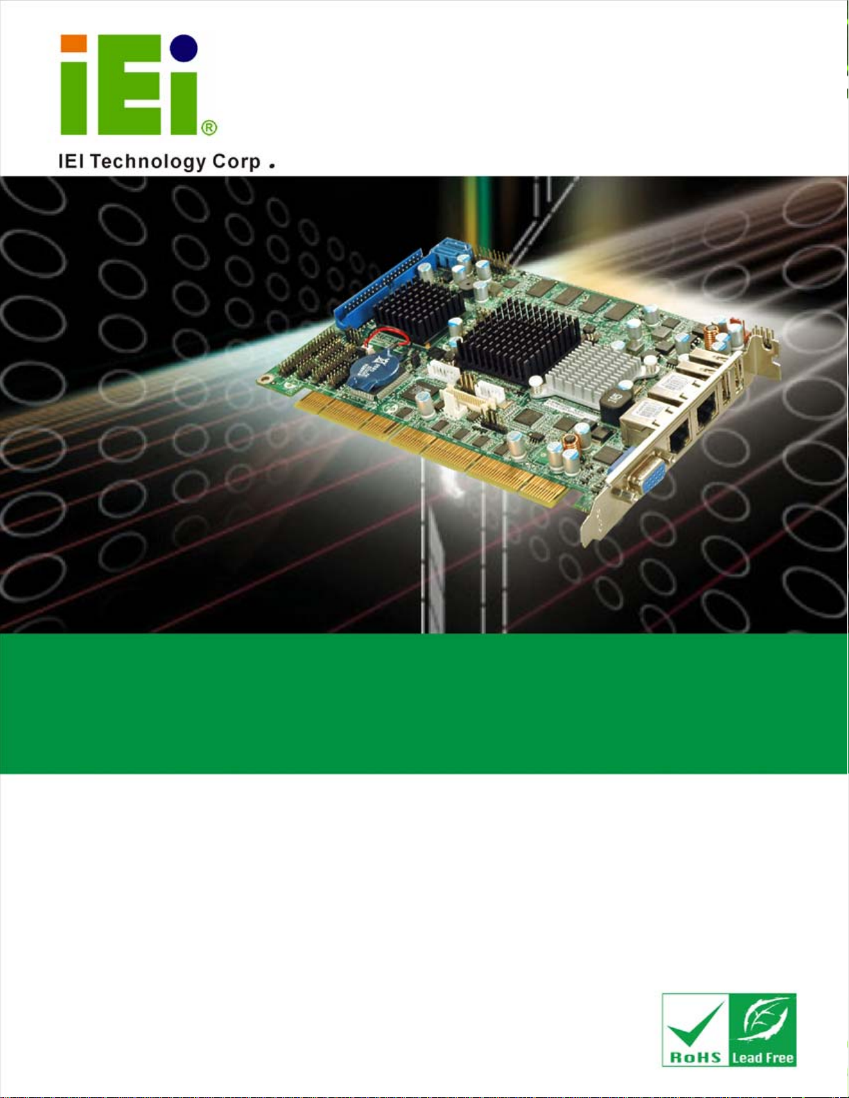
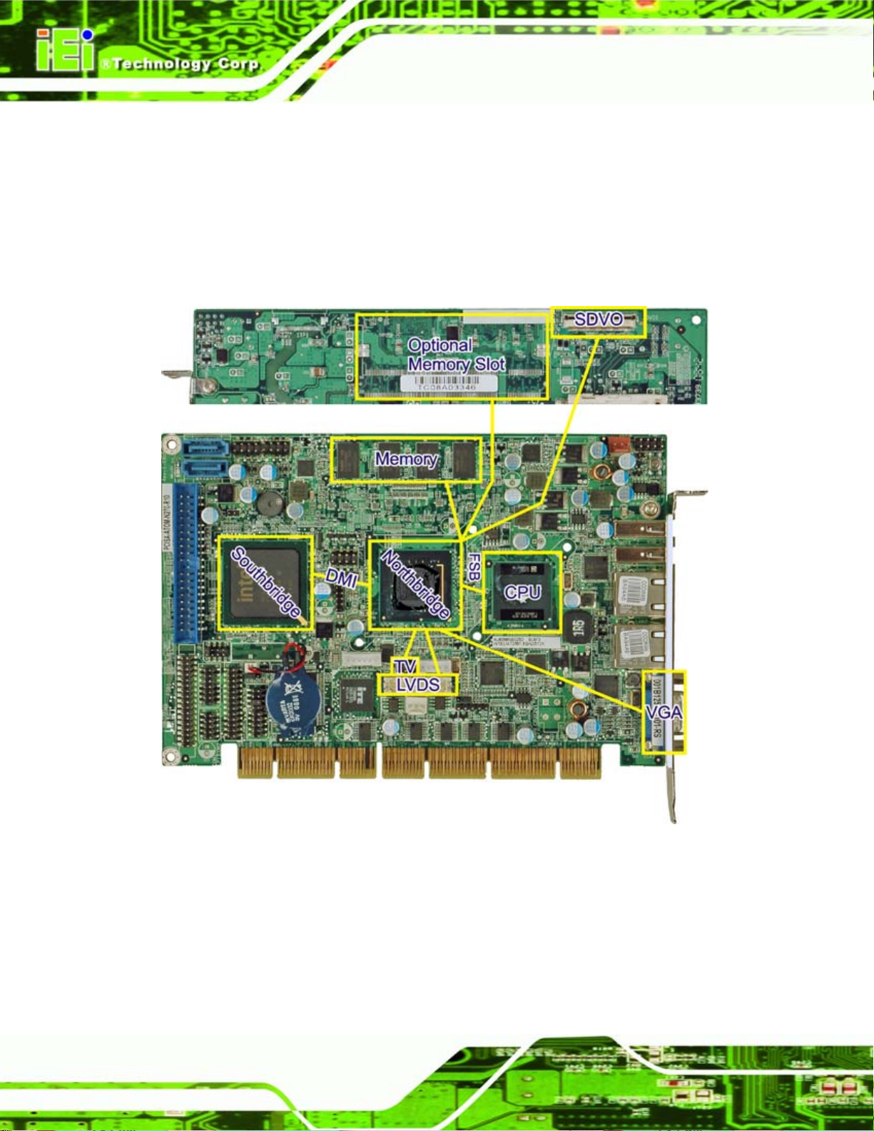
Figure 1-1: PCISA-945GSE
The PCISA-945GSE is a PCISA CPU card with an embedded 45 nm Intel® Atom™
processor. The embedded Intel® Atom™ N270 processor has a 1.60 GHz clock speed,
PCISA-945GSE CPU Card
533 MHz FSB and 512 KB of L2 cache.
The PCISA-945GSE includes four graphics outputs. VGA on the rear panel provides b asic
output capabilities for use with most monitors. Internally, an LVDS header provides a
connection to LCD displays for integrating the PCISA-945GSE into a system with built-in
monitor. The TV header provides output to a standard TV or HDTV through the optional
adapter cables, which provide a single cable connection on a card slot and a cable
splitting the signal into the component parts. Finally, an SDVO connecto r provid es a direct
connection from the Northbridge SDVO port to an IEI SDVO graphics card.
512 MB of DDR2 memory is included with the PCISA-945GSE (a custom option with a
DDR2 SO-DIMM slot is available). Permanent storage is provided through dual SATA
ports, offering 150 MB/s transfer speeds. Legacy IDE connectivity is available through an
IDE port, and through a CompactFlash® card located on the solder side of the
PCISA-945GSE.
Other connectors on the PCISA-945GSE include six USB ports (two external, four
internal), an RS-232 port, an RS-232/422/485 port, LPT and digital I/O. An HD Audio
Page 2
connector connects to an external audio kit, providing HD audio or AC’97 audio
capabilities with the appropriate audio kit.
Page 21
PCISA-945GSE CPU Card
1.2 Overview Photo
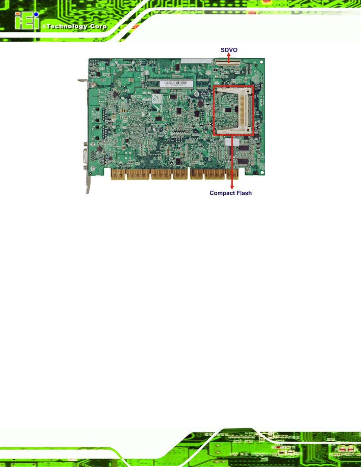
The PCISA-945GSE has a wide variety of peripheral interface connectors. 7Figure 1-2 is a
labeled photo of the peripheral interface connectors on the PCISA-945GSE.
Figure 1-2: PCISA-945GSE Overview (Front)
Page 3
Page 22
PCISA-945GSE CPU Card
Figure 1-3: PCISA-945GSE Overview (Rear)
1.3 Peripheral Connectors and Jumpers
The PCISA-945GSE has the following connectors on-board:
1 x ATX power control connector
1 x Audio kit connector
1 x Backlight inverter connector
1 x Battery connector
1 x BIOS programming header
1 x CompactFlash® slot
1 x Digital I/O connector
1 x Edge connector
1 x Fan connector
1 x Floppy disk connector
1 x Front panel connector
Page 4
1 x IDE connector
1 x Infrared connector
1 x Keyboard / mouse connector
1 x LVDS connector
Page 23
PCISA-945GSE CPU Card
1 x Parallel port connector
1 x RS-232 connector
1 x RS-232/422/485 connector
2 x SATA connectors
1 x SDVO connector
1 x TV connector
2 x USB connectors
The PCISA-945GSE has the following external peripheral interface connectors on the
board rear panel.
2 x Network ports
2 x USB ports
1 x VGA port
The PCISA-945GSE has the following on-board jumpers:
ATX power control
Clear CMOS
COM2 port mode
CompactFlash® card setup
LCD panel type selector
LCD voltage selector
1.4 Technical Specifications
PCISA-945GSE technical specifications are listed in 7Table 1-1. See Chapter 2 for details.
Specification PCISA-945GSE
Form Factor
System CPU
Front Side Bus (FSB)
PCISA
45 nm 1.60 GHz Intel® Atom™ N27 0
533 MHz
System Chipset
Northbridge: Intel® 945GSE
Southbridge: Intel® ICH7M
Page 5
Page 24
Specification PCISA-945GSE
PCISA-945GSE CPU Card
Memory
CompactFlash®
Super I/O
Display
BIOS
Audio
LAN
COM
USB2.0
512 MB of DDR2 RAM integrated (a DDR2 SO-DIMM slot is a
custom option)
One CompactFlash® socket
iTE IT8718F
VGA
LVDS
HDTV
SDVO
AMI BIOS label
Through HD Audio or AC’97 audio kit
Two Realtek RTL8111 CP PCIe GbE controllers
One RS-232 serial port
One RS-232/422/485 serial port
Six USB 2.0 devices supported (four internal, two external)
Hard Drives
SATA
Keyboard/mouse
Digital I/O
Watchdog Timer
Infrared
Power Supply
Power Consumption
Temperature
Humidity (operating)
One 40-pin IDE connector
Two 1.5 Gb/s SATA drives supported
Internal PS/2 keyboard/mouse connector
One 8-bit digital I/O connector
Software programmable 1-255 sec.
One infrared connector supports
Serial Infrared (SIR)
Amplitude Shift Keyed IR (ASKIR)
ATX and AT power supported
5 V @ 2.79 A
12 V @ 0.20 A
(with 512 MB DDR2 memory)
0ºC – 60ºC (32ºF - 140ºF)
5%~95% non-condensing
Page 6
Page 25
PCISA-945GSE CPU Card
Specification PCISA-945GSE
Dimensions (LxH)
Weight (GW/NW)
Table 1-1: Technical Specifications
185 mm x 127.6 mm
1000 g / 252 g
Page 7
Page 26
PCISA-945GSE CPU Card
Chapter
2
2 Detailed Specifications
Page 8
Page 27
PCISA-945GSE CPU Card
2.1 Dimensions
2.1.1 Board Dimensions
The dimensions of the board are listed below:
Length: 185 mm
Height: 127.6 mm
Figure 2-1: PCISA-945GSE Dimensions (mm)
Page 9
Page 28
2.1.2 External Interface Panel Dimensions
External peripheral interface connector panel dimensions are shown in 7Figure 2-2.
Figure 2-2: External Interface Panel Dimensions (mm)
PCISA-945GSE CPU Card
Page 10
Page 29
PCISA-945GSE CPU Card
2.2 Data Flow
Figure 2-3 shows the data flow between the two on-board chipsets and other components
installed on the motherboard and described in the following sections of this chapter.
Figure 2-3: Data Flow Block Diagram
Page 11
Page 30
2.3 Intel® Atom™ Processor
2.3.1 Overview
The PCISA-945GSE comes with an embedded 45 nm 1.60 GHz Intel® Atom™ N270
processor. The processor supports a 533 MHz FSB and has a 512 KB L2 cache. The low
PCISA-945GSE CPU Card
power processor has a maximum power of 2.5 W. The CPU is shown in
Figure 2-4 below.
Figure 2-4: CPU and Northbridge Connections
2.3.2 Features
Some of the features of the Intel® Atom™ N270 are listed below
Page 12
On-die, primary 32-kB instructions cache and 24-kB write-back data cache
Page 31

PCISA-945GSE CPU Card
533 MHz source-synchronous front side bus (FSB)
2-Threads support
On-die 512-kB, 8-way L2 cache
Support for IA 32-bit architecture
Intel® Streaming SIMD Extensions-2 and -3 (Intel® SSE2 and Intel® SSE3)
support and Supplemental Streaming SIMD Extension 3 (SSSE3) support
Micro-FCBGA8 packaging technologies
Thermal management support via Intel® Thermal Monitor 1 and Intel Thermal
Monitor 2
FSB Lane Reversal for flexible routing
Supports C0/C1(e)/C2(e)/C4(e)
L2 Dynamic Cache Sizing
Advanced power management features including Enhanced Intel
SpeedStep® Technology
Execute Disable Bit support for enhanced security
2.3.3 Front Side Bus (FSB)
The Intel® Atom™ processor on the PCISA-945GSE is interfaced to the Intel® 945GSE
Northbridge through a 533 MHz front side bus (FSB). The FSB is shown in
above.
2.4 Intel® 945GSE Northbridge Chip
The Intel® 945GSE Graphics and Memory Controller Hub (GMCH) supports the
embedded Intel® Atom™ N270 processor. The Intel® 945GSE is interfaced to the
processor through a 533 MHz FSB. The Northbridge connections ar e shown in
and described below.
2.4.1 DDR2 Controller
There is 512 MB of memory on the PCISA-945GSE. The memory has the following
specifications:
Figure 2-4
Figure 2-4
512 MB embedded (up to 2.0 GB can be installed on customized board with
SO-DIMM slot)
Support for DDR2 at 400 MHz and 533 MHz
Page 13
Page 32

No support for Dual-Channel Interleaved mode of operation
Enhanced Addressing support (Swap only)
PCISA-945GSE CPU Card
The embedded memory is shown in
Figure 2-4 above.
2.4.2 Graphics
The Intel® 945GSE Northbridge chipset has an Intel® Gen. 3.5 integrated graphics
engine that supports the following display devices:
Analog CRT
LVDS
TV-Out
SDVO ports
2.4.2.1 Analog CRT (VGA)
A DB-15 VGA connector on the external peripheral interface connector panel is interfaced
to the Intel® 945GSE graphics engine. The Intel® 945GSE internal graphics engine, with
an integrated 400 MHz RAMDAC and hot plug CRT support, supports analog CRT
monitors up to QXGA.
2.4.2.2 LVDS
A 30-pin LVDS crimp connector is interfaced to the Intel® 945GSE graphics engine. The
Intel® 945GSE internal graphics engine supports LVDS displays with the following
features:
Up to UXGA monitors with a maximum resolution of 1600 x 1200
18-bit 25 MHz to 112 MHz single-channel or dual-channel LVDS screens
CPIS 1.5 compliant LVDS screens
2.4.2.3 TV Out
An external 7-pin DIN TV output connector is interfaced to the Intel® 945GSE graphics
engine. The Intel® 945GSE internal graphics engine has the following TV output features:
Three integrated 10-bit DACs
Macrovision support
Page 14
Page 33

PCISA-945GSE CPU Card
Overscaling
NTSC and PAL formats supported
Supports RCA or S-VIDEO connectivity
Supports HDTV with the following resolutions:
o 480p
o 720p
o 1080i
o 1080p
2.4.2.4 SDVO and DVI
The SDVO port on the solder side of the PCISA-945GSE connects directly to the SDVO
output on the Intel® 945GSE. The SDVO connector is connected to an IEI SDVO graphics
card.
Concurrent operation of PCIe x 1 with SDVO
Two SDVO p orts supported
o SDVO is muxed onto the PCIe pins
o DVI 1.0 support for external digital monitor
o Only Downstream HDCP support
o Supports TV and DVD formats
o Display hot plug support
2.5 Intel® ICH7M Southbridge Chipset
The Intel® ICH7M Southbridge chipset is connected to the Intel® 945GSE Northbridge
GMCH through the chip-to-chip Direct Media Interface (DMI). Some of the features of the
Intel® ICH7M are listed below.
Page 15
Page 34

PCISA-945GSE CPU Card
Page 16
Figure 2-5: Intel® ICH7M Southbridge Connections
Complies with PCI Express Base Specification, Revision 1.0a
Complies with PCI Local Bus Specification, Revision 2.3 and supports
33 MHz PCI operations
Supports ACPI Power Management Logic
Contains:
o Enhanced DMA controller
o Interrupt controller
o Timer functions
Integrated SATA host controller with DMA operations interfaced to two SATA
connectors on the PCISA-945GSE
Integrated IDE controller supports Ultra ATA 100/66/33
Page 35

PCISA-945GSE CPU Card
Supports the four USB 2.0 devices on the PCISA-945GSE with four UHCI
controllers and one EHCI controller
Complies with System Management Bus (SMBus) Specification, Version 2.0
Supports Audio Codec ’97 (AC’97) Revision 2.3
Supports Intel® High Definition Audio
Contains Low Pin Count (LPC) interface
Supports Firmware Hub (FWH) interface
Serial peripheral interface support
2.5.1 HD Audio Controller
The audio connector on the PCISA-945GSE is connected to the HD Audio/AC’97 audio
channel on the Intel® ICH7M. The audio connector connects to an HD Audio kit or an
AC’97 audio kit, both available as optional extras from IEI.
The HD Audio kit provides the following connectors:
7.1 channel audio output
Line input
Microphone input
The AC’97 audio kit provides the following connectors:
5.1 channel audio output
Line input
Microphone input
2.5.2 IDE Interface
The IDE interface connects with
2.5.2.1 IDE Connector ...........................................................................18
2.5.2.2 CompactFlash® Slot..................................................................18
Page 17
Page 36

PCISA-945GSE CPU Card
2.5.2.1 IDE Connector
The IDE connector on the Intel® ICH7M Southbridge connects to an IDE hard disk or
other IDE device. PIO IDE transfers up to 16 MB/s and Ultra ATA transfers of 100 MB/s.
The integrated IDE interface is able to support the following IDE HDDs:
Ultra A T A/1 00, with data transfer rates up to 100 MB/s
Ultra A T A/6 6, with data transfer rates up to 66 MB/s
Ultra A T A/3 3, with data transfer rates up to 33 MB/s
Specification Ultra ATA/100 Ultra ATA/66 Ultra ATA/33
IDE devices
PIO Mode
PIO Max Transfer Rate
DMA/UDMA designation
DMA/UDMA Max Transfer
Controller Interface
Table 2-1: Supported HDD Specifications
2 2 2
0 – 4 0 – 4 0 – 4
16.6 MB/s 16.6 MB/s 16.6 MB/s
UDMA 5 UDMA 4 UDMA 2
100 MB/s 66 MB/s 33 MB/s
5 V 5 V 5 V
2.5.2.2 CompactFlash® Slot
The CompactFlash® slot on the PCISA-945GSE is interfaced through the IDE interface on
the Intel® ICH7M Southbridge. The CompactFlash® slot is on the solder side of the
PCISA-945GSE.
2.5.3 Real Time Clock
Page 18
256 bytes of battery backed RAM is provided by the Motorola MC146818 A real time clock
(RTC) integrated into the ICH7M. The RTC operates on a 3 V battery and 32.768 KHz
crystal. The RTC keeps track of the time and stores system data even when the system is
turned off.
Page 37

PCISA-945GSE CPU Card
2.5.4 SATA Controller
The integrated SATA controller on the Intel® ICH7M Southbridge supports two SATA
drives with independent DMA operations. Two SATA controllers are connected to two
SATA connectors on the PCISA-945GSE. SATA controller specifications are listed below.
Supports two SATA drives
Supports 1.5 Gb/s data transfer speeds
Supports Serial ATA Specification, Revision 1.0a
2.5.5 USB Controller
Up to six high-speed, full-speed or low-speed USB devices are supported by the Intel®
ICH7M on the PCISA-945GSE. High-speed USB 2.0, with data transfers of up to
480 MB/s, is enabled with the Intel® ICH7M integrated Enhanced Host Controller
Interface (EHCI) compliant host controller. USB full-speed and low-speed signaling is
supported by the Intel® ICH7M integrated Universal Host Controller Interface (UHCI)
controllers.
The six USB ports implemented on the PCISA-945GSE are connected to four internal
connectors (on two headers) and two external connectors.
2.5.6 iTE IT8718F Super I/O chipset
The iTE IT8718F Super I/O chipset is connected to the Intel® ICH7M Southbridge through
the LPC bus. The iTE IT8718F is an LPC interface-based Super I/O device that comes
with Environment Controller integration.
Page 19
Page 38

Figure 2-6: Super I/O Connections
Some of the features of the iTE IT8718F chipset are listed below:
PCISA-945GSE CPU Card
ACPI and LANDesk Compliant
Enhanced Hardware Monitor
Fan Speed Controller
Two 16C550 UARTs for serial port control
One IEEE 1284 Parallel Port
Keyboard Controller
Watchdog Timer
Some of the Super I/O features are described in more detail below:
2.5.6.1 LPC Interface
The LPC interface on the Super I/O complies with the Intel® Low Pin Count Specification
Rev. 1.0. The LPC interface supports both LDRQ# and SERIRQ protocols as well as PCI
PME# interfaces.
2.5.6.2 16C550 UARTs
Page 20
The onboard Super I/O has two integrated 16C550 UARTs that can support the following:
Two standard serial ports
IrDa 1.0 and ASKIR protocols
Page 39

PCISA-945GSE CPU Card
2.5.6.3 Digital Input/Output
The input mode supports switch debouncing or programmable external IRQ routing. The
output mode supports two sets of programmable LED blinking perio ds.
2.5.6.4 Enhanced Hardware Monitor
The Super I/O Enhanced Hardware Monitor monitors three thermal inputs, VBAT
internally, and eight voltage monitor inputs. These hardware parameters are reported in
the BIOS and can be read from the BIOS Hardware Health Configuration menu.
2.5.6.5 Fan Speed Controller
The Super I/O fan speed controller enables the system to monitor the speed of the fan.
One of the pins on the fan connector is reserved for fan speed detection and interfaced to
the fan speed controller on the Super I/O. The fan speed is then reported in the BIOS.
2.5.6.6 Keyboard/Mouse Controller
The Super I/O keyboard/mouse controller can execute the 8042 instruction set. Some of
the keyboard controller features are listed below:
The 8042 instruction is compatible with a PS/2 keyboard and PS/2 mouse
Gate A20 and Keyboard reset output
Supports multiple keyboard power on events
Supports mouse double-click and/or mouse move power on events
2.5.6.7 Parallel Port
The multi-mode high-performance parallel port supports the bi-directional Standard
Parallel Port (SPP), the Enhanced Parallel Port (EPP) and the Extended Capabilities Port
(ECP) modes.
2.5.7 PCI Bus
The PCI interface on the Intel® ICH7M is compliant with the PCI Revision 2.3
implementation. The location of the edge connector is shown in
features of the PCI interface are listed below.
Figure 2-5. Some of the
Page 21
Page 40

PCI Revision 2.3 compliant
33 MHz
5 V tolerant PCI signals (except PME#)
Integrated PCI arbiter supports up to seven PCI bus masters
2.5.7.1 PCI Edge Connector
The PCI interface is connected directly to the PCI portion of the edge connector on the
PCISA-945GSE.
2.5.7.2 ISA Edge Connector
The PCI interface is connected to the ISA edge connector through the iTE IT8888G
PCI-to-ISA chip.
2.5.8 PCIe Bus
PCISA-945GSE CPU Card
The Intel® ICH7M provides four PCIe lanes. Some of these lanes are connected to the
components listed below:
Gigabit Ethernet Connector
The Gigabit Ethernet connections are shown in
Figure 2-5.
2.5.8.1 Gigabit Ethernet Connector
Two of the four PCIe lanes on the Intel® ICH7M PCIe lanes are connected to the Realtek
RTL8111CP PCIe GbE controllers.
The Realtek RTL8111CP PCIe GbE controllers combine a triple-speed IEEE 802.3
compliant Media Access Controller (MAC) with a triple-speed Ethernet transceiver, 32-bit
PCIe bus controller, and embedded memory. With state-of-the-art DSP technology and
mixed-mode signal technology, they offer high-speed transmission over CAT 5 UTP cable
or CAT 3 UTP (10 Mb/s only) cable. Functions such as Crossover Detection &
Auto-Correction, polarity correction, adaptive equalization, cross-talk cancellation, echo
Page 22
cancellation, timing recovery, and error correction are implemented to provide robust
transmission and reception capability at high speeds.
Some of the features of the Realtek RTL8111CP PCIe GbE controllers are listed below.
Page 41

PCISA-945GSE CPU Card
Integrated 10/100/1000 transceiver
Auto-Negotiation with Next Page capability
Supports PCI Express™ 1.1
Supports pair swap/polarity/skew correction
Crossover Detection & & Auto-Correction
Wake-on-LAN and remote wake-up support
Microsoft® NDIS5, NDIS6 Checksum Offload (IPv4, IPv6, TCP, UDP) and
Segmentation Task-offload (Large send and Giant send) support
Supports Full Duplex flow control (IEEE 802.3x)
Fully compliant with IEEE 802.3, IEEE 802.3u, IEEE 802.3ab
Supports IEEE 802.1P Layer 2 Priority Encoding
Supports IEEE 802.1Q VLAN tagging
Serial EEPROM
Transmit/Receive on-chip buffer suppo rt
Supports power down/link down power saving
Supports PCI MSI (Message Signaled Interrupt) and MSI-X
Supports Receive-Side Scaling (RSS)
2.5.9 SPI Bus Components
The Intel® ICH7M SPI bus is connected to components listed below:
BIOS chip
2.5.9.1 SPI BIOS
The 4-pin Serial Peripheral Interface (SPI) is connected to an SPI BIOS chip. A licensed
copy of AMI BIOS is preinstalled on the SPI BIOS chip. A master-slave protocol is used for
communication on the SPI bus. The slave is connected to the Intel® ICH7M and is
implemented as a tri-state bus. The SPI BIOS is located on the reverse side of the JSPI1
jumper.
Page 23
Page 42

PCISA-945GSE CPU Card
2.6 Environmental and Power Specifications
2.6.1 System Monitoring
Two thermal inputs on the PCISA-945GSE Super I/O Enhanced Hardware Monitor
monitors the following temperatures:
CPU temperature
System temperature
The PCISA-945GSE Super I/O Enhanced Hardware Monitor also monitors the following
fan speeds:
CPU Fan speed
Voltage inputs on the PCISA-945GSE Super I/O Enhanced Hardware Monitor monitors
the following voltages:
CPU Core
+1.05 V
+3.30 V
+5.00 V
+12 V
+1.5 V
+1.8 V
+5 VSB
VBAT
The values for the above environmental parameters are all recorded in the BIOS
Hardware Health Configuration menu.
2.6.2 Operating Temperature and Temperature Control
The maximum and minimum operating temperatures for the PCISA-945GSE are listed
Page 24
below.
Minimum Operating Temperature: 0ºC (32°F)
Maximum Operating Temperature: 60°C (140°F)
Page 43

PCISA-945GSE CPU Card
A cooling fan and heat sink must be installed on the CPU. Thermal paste must be
smeared on the lower side of the heat sink before it is mounted on the CPU. Heat sinks
are also mounted on the Northbridge and Southbridge chipsets to ensure the operating
temperature of these chips remain low.
2.6.3 Power Consumption
7Table 2-2 shows the power consumption parameters for the PCISA-945GSE running with
a 1.60 GHz Intel® Atom™ with 2.0 GB DDR2 memory.
Voltage Current
+5 V 2.79 A
+12 V 0.20 A
Table 2-2: Power Consumption
Page 25
Page 44

PCISA-945GSE CPU Card
Chapter
3
3 Unpacking
Page 26
Page 45

PCISA-945GSE CPU Card
3.1 Anti-static Precautions
WARNING!
Failure to take ESD precautions during the installation of the
PCISA-945GSE may result in permanent damage to the
PCISA-945GSE and severe injury to the user.
Electrostatic discharge (ESD) can cause serious damage to electronic components,
including the PCISA-945GSE. Dry climates are especially susceptible to ESD. It is
therefore critical that whenever the PCISA-945GSE, or any other electrical component is
handled, the following anti-static precautions are strictly adhered to.
Wear an anti-static wristband: - Wearing a simple anti-static wristband can
help to prevent ESD from damaging the board.
Self-grounding:- Before handling the board touch any grounded conducting
material. During the time the board is handled, frequently touch any
conducting materials that are connected to the ground.
Use an anti-static pad: When configuring the PCISA-945GSE, place it on an
antic-static pad. This reduces the possibility of ESD damaging the
PCISA-945GSE.
Only handle the edges of the PCB:- When handling the PCB, hold the PCB
by the edges.
3.2 Unpacking
3.2.1 Unpacking Precautions
When the PCISA-945GSE is unpacked, please do the following:
Follow the anti-static precautions outlined in Section 76
Make sure the packing box is facing upwards so the PCISA-945GSE does not
73.1.
fall out of the box.
Make sure all the components shown in Section 76
73.3 are present.
Page 27
Page 46

3.3 Unpacking Checklist
NOTE:
If any of the components listed in the checklist below are missing, do
not proceed with the installation. Contact the IEI reseller or vendor the
PCISA-945GSE was purchased from or contact an IEI sales
PCISA-945GSE CPU Card
representative directly by sending an email to
3.3.1 Package Contents
The PCISA-945GSE is shipped with the following components:
Quantity Item and Part Number Image
1 PCISA-945GSE
2 SATA cable
(P/N: 32000-062800-RS)
1 LPT and RS-232 cable
(P/N: 19800-000027-RS)
3sales@iei.com.tw.
Page 28
1 USB cable
(P/N: CB-USB02-RS)
1 Mini jumper pack (2.0 mm)
(P/N:33100-000033-RS)
1 Utility CD
Page 47

PCISA-945GSE CPU Card
Quantity Item and Part Number Image
1 Quick Installation Guide
Table 3-1: Packing List
3.3.2 Optional Items
The PCISA-945GSE is shipped with the following components:
Item and Part Number Image
5.1 Channel AC’97 audio kit
(P/N: AC-KIT08R-R10)
7.1 Channel HD Audio kit
(P/N: AC-KIT-883HD-R10)
Dual USB cable (wo bracket)
(P/N: 32000-044300-RS)
Dual RS-232 cable
(P/N: 32200-000077-RS)
TV-out cable
(P/N: 19800-000067-RS)
HDTV output cable
(P/N: 32000-083701-RS)
KB/MS cable
(P/N: 19800-000075-RS)
Page 29
Page 48

Item and Part Number Image
FDD cable
(P/N: 32200-000058-RS)
HDD cable
PCISA-945GSE CPU Card
(P/N: 32200-000009-RS)
IDE-cable
(P/N: 32200-008800-RS)
SATA power cable
(P/N: 32100-088600-RS)
Table 3-2: Power Consumption
Page 30
Page 49

PCISA-945GSE CPU Card
Chapter
4
4 Connectors
Page 31
Page 50

4.1 Peripheral Interface Connectors
This chapter outlines all internal and external connectors on the PCISA-945GSE.
4.1.1 Layout
7Figure 4-1 shows the on-board peripheral connectors, rear panel peripheral connectors
and on-board jumpers.
PCISA-945GSE CPU Card
Page 32
Figure 4-1: Connector and Jumper Locations [Front Side]
Page 51

PCISA-945GSE CPU Card
Figure 4-2 shows the connectors on the solder side of the PCISA-945GSE.
Figure 4-2: Connector and Jumper Locations [Solder Side]
4.1.2 Internal Peripheral Interface Connectors
7Table 4-1 shows a list of the peripheral interface connectors on the PCISA-945GSE.
Detailed descriptions of these connectors can be found below.
Connector Type Label
ATX power control connector 3-pin wafer ATXCTL1
Audio kit connector 9-pin header J_AUDIO1
Backlight inverter connector 5-pin box header INVERTER1
Battery connector 2-pin box header BT1
BIOS programming connector 8-pin header JSPI1
CompactFlash® slot CF slot CF1
Digital I/O connector 10-pin header DIO1
Page 33
Page 52

Connector Type Label
Fan connector 3-pin wafer CPU_FAN1
Floppy disk connector 34-pin header FDD1
Front panel connector 8-pin header F_PANEL1
IDE connector 40-pin IDE connector PIDE1
Infrared connector 5-pin header IR1
Keyboard/mouse connector 6-pin box header KB_MS1
LVDS connector 30-pin crimp LVDS1
Parallel port connector 26-pi n header LPT1
RS-232 connector 10-pin header COM1
RS-232/422/485 connector 14-pin header COM2
SATA connector SATA port SATA1, SATA2
PCISA-945GSE CPU Card
SDVO connector Flat cable connector SDVO1
TV connector 6-pin header TV1
USB connectors 8-pin header USB01, USB23
Table 4-1: Peripheral Interface Connectors
4.1.3 External Interface Panel Connectors
7Table 4-2 lists the rear panel connectors on the PCISA-945GSE. Detailed descriptions of
these connectors can be found in Section 1H
Connector Type Label
Network ports RJ-45 LAN1, LAN2
USB ports USB port USB_C4, USB_C5
VGA port VGA port VGA1
Table 4-2: Rear Panel Connectors
4.3 on page 757.
Page 34
Page 53

PCISA-945GSE CPU Card
4.2 Internal Peripheral Connectors
Internal peripheral connectors are found on the motherboard and are only accessible
when the motherboard is outside of the chassis. T his se ction h as complet e d esc ription s of
all the internal, peripheral connectors on the PCISA-945GSE.
4.2.1 ATX Power Control Connector
CN Label: ATXCTL1
CN Type:
CN Location:
CN Pinouts:
The ATX power supply enable connector enables the PCISA-945GSE to be connected to
an ATX power supply. In default mode, the PCISA-945GSE can only us an AT power
supply. To enable an ATX power supply the AT Power Select jumper must also be
configured. Please refer to Chapter 3 for more details.
3-pin wafer (1x3)
Figure 4-3
See
Table 4-3
See
Figure 4-3: ATX Power Supply Enable Connector Location
PIN NO. DESCRIPTION
1 GND
2 PS-ON
Page 35
Page 54

PIN NO. DESCRIPTION
3 +5 V Standby
Table 4-3: ATX Power Supply Enable Connector Pinouts
4.2.2 Audio Connector
CN Label: J_AUDIO1
PCISA-945GSE CPU Card
CN Type:
CN Location:
CN Pinouts:
9-pin header (2x5)
Figure 4-4
See
Table 4-4
See
The 9-pin audio connector is connected to external audio devices including speakers and
microphones for the input and output of audio signals to and from the system.
Page 36
Figure 4-4: Audio Connector Location (9-pin)
PIN NO. DESCRIPTION PIN NO. DESCRIPTION
1 SYNC 2 BITCLK
3 SDOUT 4 PCBEEP
5 SDIN 6 RST#
7 VCC 8 GND
Page 55

PCISA-945GSE CPU Card
PIN NO. DESCRIPTION PIN NO. DESCRIPTION
9 +12 V
Table 4-4: Audio Connector Pinouts (9-pin)
4.2.3 Backlight Inverter Connector
CN Label: INVERTER1
CN Type:
CN Location:
CN Pinouts:
5-pin box header (1x5)
Figure 4-5
See
Table 4-5
See
The backlight inverter provides power to the LCD screen backlight.
Figure 4-5: LCD Backlight Connector Pinout Locations
PIN NO. DESCRIPTION
1 Brightness
2 GND
3 12 V
4 GND
5 Backlight enable
Table 4-5: LCD Backlight Connector Pinouts
Page 37
Page 56

4.2.4 Battery Connector
CN Label: BT1
PCISA-945GSE CPU Card
CN Type:
CN Location:
CN Pinouts:
The battery connector is for the system battery. The battery retains the system date and
time while the computer is turned off.
2-pin wafer (1x2)
Figure 4-6
See
Table 4-6
See
Figure 4-6: Battery Connector Location
PIN NO. DESCRIPTION
1 Battery+
2 Battery-
Table 4-6: Battery Connector Pinouts
4.2.5 BIOS Programming Connector
CN Label: JSPI1
8-pin header (2x4)
Figure 4-7
See
Table 4-7
See
Page 38
CN Type:
CN Location:
CN Pinouts:
Page 57

PCISA-945GSE CPU Card
The 8-pin SPI Flash connector is used for the BIOS.
Figure 4-7: BIOS Programming Connector Pinouts
PIN DESCRIPTION PIN DESCRIPTION
1 3.3 V 2 GND
3 CS# 4 CLOCK
5 SO 6 SI
7 N/C 8 N/C
Table 4-7: BIOS Programming Connector
4.2.6 CompactFlash® Socket
CN Label: CF1
CN Type:
CN Location:
CN Pinouts:
The CompactFlash® card slot allows a CompactFlash® type I or II card to be installed.
CompactFlash® slot
Figure 4-8
See
Table 4-8
See
Page 39
Page 58

PCISA-945GSE CPU Card
Figure 4-8: CF Card Socket Location
PIN NO. DESCRIPTION PIN NO. DESCRIPTION
1 GROUND 26 CD1#
2 DATA 3 27 DATA 11
3 DATA 4 28 DATA 12
4 DATA 5 29 DATA 13
5 DATA 6 30 DATA 14
6 DATA 7 31 DATA 15
7 CE# 32 CE2#
8 A10 33 VS1#
9 OE# 34 IOR#
10 A9 35 IOW#
11 A8 36 WE#
12 A7 37 IRQ
13 VCC1 38 VCC2
14 A6 39 CSEL#
15 A5 40 VS2#
16 A4 41 RESET#
17 A3 42 WAIT#
18 A2 43 INPACK#
19 A1 44 REG#
20 A0 45 BVD2
Page 40
21 DATA 0 46 BVD1
22 DATA 1 47 DATA 8
23 DATA 2 48 DATA 9
24 IOCS16# 49 DATA 10
Page 59

PCISA-945GSE CPU Card
PIN NO. DESCRIPTION PIN NO. DESCRIPTION
25 CD2# 50 GND2
Table 4-8: CF Card Socket Pinouts
4.2.7 Digital I/O Connector
CN Label: DIO1
CN Type:
CN Location:
CN Pinouts:
10-pin header (2x5)
Figure 4-9
See
Table 4-9
See
The digital input/output connector is managed through a Super I/O chip. The DIO
connector pins are user programmable.
Figure 4-9: Digital I/O Connector Locations
PIN NO. DESCRIPTION PIN NO. DESCRIPTION
1 GND 2 VCC
3 Output 3 4 Output 2
5 Output 1 6 Output 0
7 Input 3 8 Input 2
Page 41
Page 60

PIN NO. DESCRIPTION PIN NO. DESCRIPTION
9 Input 1 10 Input 0
Table 4-9: DIO Connector Pinouts
4.2.8 Fan Connector
CN Label: CPU_FAN1
PCISA-945GSE CPU Card
CN Type:
CN Location:
CN Pinouts:
3-pin wafer (1x3)
7Figure 4-10
See
7Table 4-10
See
The fan connector connects to a CPU cooling fan.
Figure 4-10: CPU Fan Connector Location
PIN NO. DESCRIPTION
1 Ground
2 +12 V
3 Sense
Table 4-10: CPU Fan Connector Pinouts
4.2.9 Floppy Disk Connector
CN Label: FDD1
Page 42
Page 61

PCISA-945GSE CPU Card
CN Type:
CN Location:
CN Pinouts:
34-pin header (2x17)
Figure 4-11
See
Table 4-11
See
The floppy disk connector is connected to a floppy disk drive.
Figure 4-11: Floppy Disk Connector Location
PIN NO. DESCRIPTION PIN NO. DESCRIPTION
1 GND 2 REDUCE W RITE
3 GND 4 N/C
5 N/C 6 N/C
7 GND 8 INDEX#
9 GND 10 MOTOR ENABLE A#
11 GND 12 DRIVE SELECT B#
13 GND 14 DRIVE SELECT A#
15 GND 16 MOTOR ENABLE B#
17 GND 18 DIRECTION#
19 GND 20 STEP#
21 GND 22 WRITE DATA#
23 GND 24 WRITE GATE#
Page 43
Page 62

PIN NO. DESCRIPTION PIN NO. DESCRIPTION
25 GND 26 TRACK 0#
27 GND 28 WRITE PROTECT#
29 GND 30 READ DATA#
31 GND 32 SIDE 1 SELECT#
33 GND 34 DISK CHANGE#
Table 4-11: Floppy Disk Connector Pinouts
4.2.10 Front Panel Connector
CN Label: F_PANEL1
PCISA-945GSE CPU Card
CN Type:
CN Location:
CN Pinouts:
8-pin header (2x4)
Figure 4-12
See
Table 4-12
See
The front panel connector connects to external switches and indicators to monitor and
controls the motherboard. These indicators and switches include:
Power button
Reset
Power LED
HDD LED
Page 44
Page 63

PCISA-945GSE CPU Card
Figure 4-12: Front Panel Connector Pinout Locations
FUNCTION PIN DESCRIPTION FUNCTION PIN DESCRIPTION
Power button 1 PWR_BTN+ Power LED 2 PWR_LED+
3 PWR_BTN- 4 PWR_LEDHDD LED 5 HDD_LED+ Reset button 6 RESET+
7 HDD_LED- 8 RESET-
Table 4-12: Front Panel Connector Pinouts
4.2.11 IDE Connector
CN Label: IDE1
CN Type:
CN Location:
CN Pinouts:
The IDE connector can connect to up to two IDE devices like hard drives or optical drives.
40-pin header (2x20)
7Figure 4-13
See
7Table 4-13
See
Page 45
Page 64

PCISA-945GSE CPU Card
Figure 4-13: IDE Device Connector Locations
PIN NO. DESCRIPTION PIN NO. DESCRIPTION
1 RESET# 2 GROUND
3 DATA 7 4 DATA 8
5 DATA 6 6 DATA 9
7 DATA 5 8 DATA 10
9 DATA 4 10 DATA 11
11 DATA 3 12 DATA 12
13 DATA 2 14 DATA 13
15 DATA 1 16 DATA 14
17 DATA 0 18 DATA 15
19 GROUND 20 N/C
21 IDE DRQ 22 GROUND
23 IOW# 24 GROUND
25 IOR# 26 GROUND
27 IDE CHRDY 28 BALE-DEFAULT
29 IDE DACK 30 GROUND–DEFAULT
31 INTE RRUPT 32 N/C
33 SA1 34 PDIAG#
Page 46
35 SA0 36 SA2
37 HDC CS0# 38 HDC CS1#
Page 65

PCISA-945GSE CPU Card
PIN NO. DESCRIPTION PIN NO. DESCRIPTION
39 HDD ACTIVE # 40 GROUND
Table 4-13: IDE Connector Pinouts
4.2.12 Infrared Interface Connector
CN Label: IR1
CN Type:
CN Location:
CN Pinouts:
5-pin header (1x5)
7Figure 4-14
See
7Table 4-14
See
The infrared interface connector supports both Serial Infrared (SIR) and Amplitude Shift
Key Infrared (ASKIR) interfaces.
Figure 4-14: Infrared Connector Pinout Locations
PIN NO. DESCRIPTION
1 VCC
2 NC
3 IR-RX
4 GND
5 IR-TX
Table 4-14: Infrared Connector Pinouts
Page 47
Page 66

4.2.13 Keyboard/Mouse Connector
CN Label: KB_MS1
PCISA-945GSE CPU Card
CN Type:
CN Location:
CN Pinouts:
6-pin box header (1x6)
Figure 4-15
See
Table 4-15
See
The keyboard and mouse connector can be connected to a standard PS/2 cable or PS/2
Y-cable to add keyboard and mouse functionality to the system.
Figure 4-15: Keyboard/Mouse Connector Location
PIN NO. DESCRIPTION
1 +5 V
2 Mouse data
3 Mouse clock
4 Keyboard data
5 Keyboard clock
6 Ground
Table 4-15: Keyboard/Mouse Connector Pinouts
4.2.14 LVDS LCD Connector
CN Label: LVDS1
Page 48
Page 67

PCISA-945GSE CPU Card
CN Type:
CN Location:
CN Pinouts:
30-pin crimp (2x15)
Figure 4-16
See
Table 4-16
See
The 30-pin LVDS LCD connector can be connected to single channel or dual channel,
18-bit or 36-bit LVDS panel.
Figure 4-16: LVDS LCD Connector Pinout Locations
PIN NO. DESCRIPTION PIN NO. DESCRIPTION
1 GROUND 2 GROUND
3 LVDSA_Y0+ 4 LVDSA_Y05 LVDSA_Y1+ 6 LVDSA_Y17 LVDSA_Y2+ 8 LVDSA_Y29 LVDSA_CLK+ 10 LVDSA_CLK11 NC 12 NC
13 GROUND 14 GROUND
15 LVDSB_Y0+ 16 LVDSB_Y017 LVDSB_Y1+ 18 LVDSB_Y119 LVDSB_Y2+ 20 LVDSB_Y221 LVDSB_CLK+ 22 LVDSB_CLK23 NC 24 NC
25 GROUND 26 GROUND
27 VCC_LVDS 28 VCC_LVDS
Page 49
Page 68

PIN NO. DESCRIPTION PIN NO. DESCRIPTION
29 VCC_LVDS 30 VCC_LVDS
Table 4-16: LVDS LCD Port Connector Pinouts
4.2.15 SATA Drive Connectors
CN Label: SATA1, SATA2
PCISA-945GSE CPU Card
CN Type:
CN Location:
CN Pinouts:
7-pin SATA drive connectors
7Figure 4-17
See
7Table 4-17
See
The SATA connectors connect to SATA hard drives and optical drives.
Page 50
Figure 4-17: SATA Drive Connector Locations
PIN NO. DESCRIPTION
1 GND
2 TX+
3 TX4 GND
5 RX6 RX+
Page 69

PCISA-945GSE CPU Card
PIN NO. DESCRIPTION
7 GND
Table 4-17: SATA Drive Connector Pinouts
4.2.16 Parallel Port Connector
CN Label: LPT1
CN Type:
CN Location:
CN Pinouts:
26-pin header (2x13)
Figure 4-18
See
Table 4-18
See
The 26-pin parallel port connector connects to a parallel port connector interface or some
other parallel port device such as a printer.
Figure 4-18: Parallel Port Connector Location
PIN NO. DESCRIPTION PIN NO. DESCRIPTION
1 STROBE# 2 DATA 0
3 DATA 1 4 DATA 2
5 DATA 3 6 DATA 4
7 DATA 5 8 DATA 6
9 DATA 7 10 ACKNOWLEDGE
11 BUSY 12 PAPER EMPTY
Page 51
Page 70

PIN NO. DESCRIPTION PIN NO. DESCRIPTION
13 PRINTER SELECT 14 AUTO FORM FEED #
15 ERROR# 16 INITIALIZE
17 PRINTER SELECT LN# 18 GROUND
19 GROUND 20 GROUND
21 GROUND 22 GROUND
23 GROUND 24 GROUND
25 GROUND 26 NC
Table 4-18: Parallel Port Connector Pinouts
4.2.17 Serial Port Connector (RS-232)
CN Label: COM1
PCISA-945GSE CPU Card
CN Type:
CN Location:
CN Pinouts:
10-pin header (2x5)
7Figure 4-19
See
7Table 4-19
See
The 10-pin serial port connector provides an RS-232 serial communications channel.
Figure 4-19: RS-232 Connector Pinout Locations
PIN NO. DESCRIPTION PIN NO. DESCRIPTION
1 Data Carrier Direct (DCD) 2 Data Set Ready (DSR)
Page 52
3 Receive D ata (RXD) 4 Request To Send (RTS)
5 Transmit Data (TXD) 6 Clear To Send (CTS)
7 Data Terminal Ready (DTR) 8 Ring Indicator (RI)
Page 71

PCISA-945GSE CPU Card
PIN NO. DESCRIPTION PIN NO. DESCRIPTION
9 Ground (GND) 10 N/C
Table 4-19: RS-232 Connector Pinouts
4.2.18 Serial Port Connector (RS-232/422/485)
CN Label: COM2
CN Type:
CN Location:
CN Pinouts:
14-pin header (2x7)
Figure 4-20
See
7Table 4-20
See
The serial port connector provides an RS-232, RS-422 or RS-485 communications
channel.
Figure 4-20: RS-232/422/485 Connector Pinout Locations
PIN NO. DESCRIPTION PIN NO. DESCRIPTION
1 Data Carrier Direct (DCD) 2 Data Set Ready (DSR)
3 Receive D ata (RXD) 4 Request To Send (RTS)
5 Transmit Data (TXD) 6 Clear To Send (CTS)
7 Data Terminal Ready (DTR) 8 Ring Indicator (RI)
9 Ground (GND) 10 Ground (GND)
11 TXD485+ 12 TXD48513 RXD485+ 14 RXD485-
Table 4-20: RS-232/422/485 Connector Pinouts
Page 53
Page 72

4.2.19 SDVO Connector
CN Label: SDVO1
PCISA-945GSE CPU Card
CN Type:
CN Location:
CN Pinouts:
FPC connector
Figure 4-21
See
Table 4-21
See
The SDVO connector connects to an SDVO video card available from IEI. The SDVO
connector interfaces directly to the SDVO port on the Northbridge.
Page 54
Figure 4-21: SDVO Connector Pinout Locations
PIN NO. DESCRIPTION PIN NO. DESCRIPTION
1 GND 2 NC
3 NC 4 GND
5 NC 6 NC
7 GND 8 SDVOB_CLK9 SDVOB_CLK+ 10 GND
11 SDVOB_GREEN- 12 SDVOB_GREEN+
13 GND 14 NC
15 NC 16 GND
17 SDVOB_I NT+ 18 SDVOB_INT+
19 GND 20 NC
21 NC 22 GND
Page 73

PCISA-945GSE CPU Card
PIN NO. DESCRIPTION PIN NO. DESCRIPTION
23 NC 24 NC
25 GND 26 SDVOB_BLUE27 SDVOB_BLUE+ 28 GND
29 SDVOB_RED- 30 SDVOB_RED+
31 GND 32 SDVO1_STALL33 SDVO1_STALL+ 34 GND
35 SDVO_TVCLKIN- 36 SDVO_TCCLKIN+
37 GND 38 SDVO_CLK
39 SDVO_DATA 40 PCIRST
41 +5 VS 42 +5 VS
43 +5 VS 44 N/C
45 N/C 46 GND
47 GND
Table 4-21: SDVO Connector Pinouts
4.2.20 TV Out Connector
CN Label: TV1
CN Type:
CN Location:
CN Pinouts:
The TV out connector connects to a TV output by using an S-Video or RCA connector.
The TV out connector makes displaying media data on a television easier.
6-pin header (2x3)
Figure 4-22
See
Table 4-22
See
Page 55
Page 74

PCISA-945GSE CPU Card
Figure 4-22: TV Connector Pinout Locations
PIN NO. DESCRIPTION PIN NO. DESCRIPTION
S-Video Connector
1 GND 2 AGREEN_Y
3 GND 4 ARED_C
RCA Connector (only video signal)
5 GND 6 ABLUE_CVBS
Table 4-22: TV Port Connector Pinouts
4.2.21 USB Connectors
CN Label: USB01, USB23
CN Type:
CN Location:
CN Pinouts:
The 2x4 USB pin connectors provide connectivity to four USB 1.1 or USB 2.0 devices.
Each USB connector can support two USB devices. Additional external USB ports are
found on the rear panel. The USB ports are used for I/O bus expansion.
8-pin header (2x4)
8Figure 4-23
See
8Table 4-23
See
Page 56
Page 75

PCISA-945GSE CPU Card
Figure 4-23: USB Connector Pinout Locations
PIN NO. DESCRIPTION PIN NO. DESCRIPTION
USB Connector 1 USB Connector 2
1 VCC 2 GND
3 DATA1- 4 DATA2+
5 DATA1+ 6 DATA27 GND 8 VCC
Table 4-23: USB Port Connector Pinouts
4.3 External Peripheral Interface Connector Panel
8Figure 4-24 shows the PCISA-945GSE external peripheral interface connector (EPIC)
panel. The PCISA-945GSE EPIC panel consists of the following:
2 x RJ-45 LAN connectors
2 x USB connectors
1 x VGA connector
Page 57
Page 76

Figure 4-24: PCISA-945GSE External Peripheral Interface Connector
4.3.1 LAN Connectors
CN Label: LAN1 and LAN2
PCISA-945GSE CPU Card
CN Type:
CN Location:
CN Pinouts:
RJ-45
8Figure 4-24
See
8Table 4-24
See
The PCISA-945GSE is equipped with two built-in RJ-45 Ethernet controllers. The
controllers can connect to the LAN through two RJ-45 LAN connectors. There are two
LEDs on the connector indicating the status of LAN. The pin assignments are listed in the
following table:
PIN DESCRIPTION PIN DESCRIPTION
1 MDIA3- 5 MDIA1+
2 MDIA3+ 6 MDIA2+
3 MDIA2- 7 MDIA04 MDIA1- 8 MDIA0+
Table 4-24: LAN Connector Pinouts
Page 58
Figure 4-25: LAN Connector
Page 77

PCISA-945GSE CPU Card
The RJ-45 Ethernet connector has two status LEDs, one green and one yello w. The green
LED indicates activity on the port and the yellow LED indicates the port is linked. See
8Table 4-25.
STATUS DESCRIPTION STATUS DESCRIPTION
GREEN Activity YELLOW Linked
Table 4-25: LAN Connector LEDs
4.3.2 USB Connectors
CN Label: USB_C4 and USB_C5
CN Type:
CN Location:
CN Pinouts:
USB port
8Figure 4-24
See
8Table 4-26
See
The PCISA-945GSE has two external USB 2.0 ports. The ports connect to both USB 2.0
and USB 1.1 devices.
PIN NO. DESCRIPTION
1 VCC
2 DATA3 DATA+
4 GND
Table 4-26: USB Port Pinouts
4.3.3 VGA Connector
CN Label: VGA1
CN Type:
CN Location:
CN Pinouts:
15-pin Female
8Figure 4-24
See
8Figure 4-26 and 8Table 4-27
See
The PCISA-945GSE has a single 15-pin female connector for connectivity to standard
display devices.
Page 59
Page 78

PCISA-945GSE CPU Card
Figure 4-26: VGA Connector
PIN DESCRIPTION PIN DESCRIPTION
1 RED 2 GREEN
3 BLUE 4 NC
5 GND 6 CRT_PLUG7 GND 8 GND
9 VCC 10 GND
11 NC 12 DDC DAT
13 HSYNC 14 VSYNC
15 DDCCLK
Table 4-27: VGA Connector Pinouts
Page 60
Page 79

PCISA-945GSE CPU Card
Chapter
5
5 Installation
Page 61
Page 80

5.1 Anti-static Precautions
WARNING:
Failure to take ESD precautions during the installation of the
PCISA-945GSE may result in permanent damage to the
PCISA-945GSE and severe injury to the user.
Electrostatic discharge (ESD) can cause serious damage to electronic components,
including the PCISA-945GSE. Dry climates are especially susceptible to ESD. It is
therefore critical that whenever the PCISA-945GSE, or any other electrical component is
handled, the following anti-static precautions are strictly adhered to.
Wear an anti-static wristband: - Wearing a simple anti-static wristband can
PCISA-945GSE CPU Card
help to prevent ESD from damaging the board.
Self-grounding:- Before handling the board touch any grounded conducting
material. During the time the board is handled, frequently touch any
conducting materials that are connected to the ground.
Use an anti-static pad: When configuring the PCISA-945GSE, place it on an
antic-static pad. This reduces the possibility of ESD damaging the
PCISA-945GSE.
Only handle the edges of the PCB:-: When handling the PCB, hold the PCB
by the edges.
Page 62
Page 81

PCISA-945GSE CPU Card
5.2 Installation Considerations
NOTE:
The following installation notices and installation considerations should
be read and understood before the PCISA-945GSE is installed. All
installation notices pertaining to the installation of the PCISA-945GSE
should be strictly adhered to. Failing to adhere to these precautions
may lead to severe damage of the PCISA-945GSE and injury to the
person installing the motherboard.
5.2.1 Installation Notices
WARNING:
The installation instructions described in this manual should be
carefully followed in order to prevent damage to the PCISA-945GSE,
PCISA-945GSE components and injury to the user.
Before and during the installation please DO the following:
Read the user manual:
o The user manual provides a complete description of the PCISA-945GSE
installation instructions and configuration options.
Wear an electrostatic discharge cuff (ESD):
o Electronic components are easily damaged by ESD. Wearing an ESD cuff
removes ESD from the body and helps prevent ESD damage.
Place the PCISA-945GSE on an antistatic pad:
o When installing or configuring the motherboard, place it on an antistatic
pad. This helps to prevent potential ESD damage.
Turn all power to the PCISA-945GSE off:
o When working with the PCISA-945GSE, make sure that it is disconnected
from all power supplies and that no electricity is being fed into the system.
Page 63
Page 82

Before and during the installation of the PCISA-945GSE DO NOT:
DO NOT remove any of the stickers on the PCB board. These stickers are
required for warranty validation.
DO NOT use the product before verifying all the cables and power connectors
are properly connected.
DO NOT allow screws to come in contact with the PCB circuit, connector pins,
or its components.
5.2.2 Installation Checklist
The following checklist is provided to ensure the PCISA-945GSE is properly installed.
All the items in the packing list are present
A compatible memory module is properly inserted into the slot
The CF Type I or CF Type II card is properly installed into the CF socket
PCISA-945GSE CPU Card
The jumpers have been properly configured
The PCISA-945GSE is inserted into a chassis with adequate ventilation
The correct power supply is being used
The following devices are properly connected
o Primary and secondary IDE device
o SATA drives
o Power supply
o USB cable
o Serial port cable
The following external peripheral devices are properly connected to the
chassis:
o VGA screen
o Keyboard
o Mouse
o USB devices
o LAN cable
5.3 Unpacking
When the PCISA-945GSE is unpacked, please check all the unpacking list items listed in
Chapter 3 are indeed present. If any of the unpacking list items are not available please
Page 64
Page 83

PCISA-945GSE CPU Card
contact the PCISA-945GSE vendor reseller/vendor where the PCISA-945GSE was
purchased or contact an IEI sales representative.
5.4 CF Card Installation
NOTE:
The PCISA-945GSE can support both CF Type I cards and CF Type II
cards. For the complete specifications of the supported CF cards
please refer to Chapter 2.
To install the a CF card (Type 1 or Type 2) onto the PCISA-945GSE, please follow the
steps below:
Step 1: Loca te the CF card socket. Place the PCISA-945GSE on an anti-static pad
with the solder side facing up. Locate the CF card.
Step 2: Align the CF card. Make sure the CF card is properly aligned with the CF
socket.
Step 3: Insert the CF card . Gently insert the CF card into the socket making sure the
socket pins are properly inserted into the socket. See
Figure 5-1. Step 0:
Page 65
Page 84

PCISA-945GSE CPU Card
Figure 5-1: CF Card Installation
5.5 ATX Power Control Connector
The ATX power control connector is required when using an ATX power source. To setup
the PCISA-945GSE for ATX power, follow the steps below.
Step 1: Set the ATX jumpers (there are two) as shown in
Section
Step 2: Conn ect the ATX control cable. Connect the A TX control ca ble to ATXCTL1 on
the PCISA-945GSE and to the ATX control connector on the backplane.
Figure 5-2)
(
5.6.1.
AT/ATX Power Selection in
Page 66
Page 85

PCISA-945GSE CPU Card
Figure 5-2: ATX Power Control Connector
Step 3: Turn on with the front panel connector. The system is turned on using the
Front Panel Connector described in Section 4.2.10. Step 3:
Page 67
Page 86

5.6 Jumper Settings
NOTE:
A jumper is a metal bridge used to close an
electrical circuit. It consists of two or three
metal pins and a small metal clip (often
protected by a plastic cover) that slides over
the pins to connect them. To CLOSE/SHORT
a jumper means connecting the pins of the
jumper with the plastic clip and to OPEN a
PCISA-945GSE CPU Card
jumper means removing the plastic clip from a
jumper.
Before the PCISA-945GSE is installed in the system, the jumpers must be set in
accordance with the desired configuration. The jumpers on the PCISA-945GSE are listed
in
Table 5-1.
Description Label Type
AT/ATX power selection ATXCTL1
J_AUTOPWR1
CF card setup JCF1 2-pin header
Clear CMOS J_CMOS 3-pin header
COM 2 function select JP1 8-pin header
LCD panel resolution selection J_LCD_TYPE1 8-pin header
Jumper Locations
3-pin wafer
2-pin header
Page 68
LVDS voltage selection J_VLVDS 3-pin header
Table 5-1: Jumpers
Page 87

PCISA-945GSE CPU Card
Figure 5-3: Jumper Location
5.6.1 AT/ATX Power Selection
Jumper Label: ATXCTL1 and J_AUTOPWR1
Jumper Type:
Jumper Settings:
Jumper Location:
The AT/ATX power selection jumpers set the system power mode as AT or ATX. Jumper
settings are shown below.
Jumper ATXCTL1 J_AUTOPWR1
AT 1-2 Short
3-pin wafer and 2-pin header
Table 5-2
See
Figure 5-3
See
Page 69
Page 88

Jumper ATXCTL1 J_AUTOPWR1
PCISA-945GSE CPU Card
ATX Connect to PS_ON#
and 5 VSB
Open
Table 5-2: AT/ATX Power Selection Jumper Settings
5.6.2 Clear CMOS Jumper
Jumper Label: J_CMOS1
Jumper Type:
Jumper Settings:
Jumper Location:
If the PCISA-945GSE fails to boot due to improper BIOS settings, the clear CMOS jumper
clears the CMOS data and resets the system BIOS information. To do this, use the jumper
cap to close pins 2 and 3 for a few seconds then reinstall the jumper clip back to pins 1
and 2.
3-pin header
8Table 5-3
See
Figure 5-3
See
If the “CMOS Settings Wrong” message is displayed during the boot up process, the fault
may be corrected by pressing the F1 to enter the CMOS Setup menu. Do one of the
following:
Enter the correct CMOS setting
Load Optimal Defaults
Load Failsafe Defaults.
After having done one of the above, save the changes and exit the CMOS Setup menu.
The clear CMOS jumper settings are shown in
AT Power Select Description
1-2 Keep CMOS Setup
2-3 Clear CMOS Setup
8Table 5-3.
Table 5-3: Clear CMOS Jumper Settings
Page 70
Page 89

PCISA-945GSE CPU Card
5.6.3 CF Card Setup
Jumper Label: JCF1
Jumper Type:
Jumper Settings:
Jumper Location:
2-pin header
Table 5-4
See
Figure 5-3
See
The CF Card Setup jumper sets the CF Type I card or CF Type II cards as either the slave
device or the master device. CF Card Setup jumper settings are shown in
CF Card Setup Description
Open Slave
Closed Master
Table 5-4.
Table 5-4: CF Card Setup Jumper Settings
5.6.4 COM2 RS-232/422/485 Selection Jumper
Jumper Label: JP1
Jumper Type:
8-pin header
Table 5-5
Jumper Settings:
Jumper Location:
See
Figure 5-3
See
The RS-232/422/485 Serial Port Select jumper sets the communication protocol used by
COM3. The RS-232/422/485 Serial Port Select settings are shown in
RS-232/422/485 Description
1-2 RS-232
3-4 RS-422
5-6 RS-485
7-8 RS-485 with RTS Control
Table 5-5.
Table 5-5: COM2 RS-232/422/485 Selection Jumper Pinouts
Page 71
Page 90

5.6.5 LCD Panel Type Selection
Jumper Label: J_LCD_TYPE1
PCISA-945GSE CPU Card
Jumper Type:
Jumper Settings:
Jumper Location:
6-pin header
Table 5-6
See
Figure 5-3
See
The LCD Panel Type Selection jumper allows the LVDS screen voltage to be set. The
LCD Panel Type Selection jumper settings are shown in
LCD Panel
Description
Selection
Open 640 x 480 (18-bit)
1-2 800 x 480 (18-bit)
3-4 800 x 600 (18-bit)
1-2 and 3-4 1024 x 768 (18-bit)
5-6 1280 x 1024 (36-bit)
1-2 and 5-6 1400 x 1050 (36-bit)
3-5 and 5-6 1400 x 900 (36-bit)
Table 5-7.
1-2, 3-4 and 5-6 1600 x 1200 (36-bit)
Table 5-6: LCD Panel Type Selection Jumper Settings
5.6.6 LVDS Voltage Selection
WARNING:
Permanent damage to the screen and PCISA-945GSE may occur if the
wrong voltage is selected with this jumper. Please refer to the user
guide that came with the monitor to select the correct voltage.
Jumper Label: J_VLVDS1
Jumper Type:
3-pin header
Page 72
Page 91

PCISA-945GSE CPU Card
Jumper Settings:
Jumper Location:
The LVDS Voltage Selection jumper allows the LVDS screen voltage to be set. The
See
Table 5-7
Figure 5-3
See
LVDS Voltage Selection jumper settings are shown in
LCD Voltage Select Description
1-2 3.3 V
2-3 5 V
Table 5-7: LVDS Voltage Selection Jumper Settings
5.7 Chassis Installation
5.7.1 Airflow
WARNING:
Airflow is critical to the cooling of the CPU and other onboard
components. The chassis in which the PCISA-945GSE must have air
vents to allow cool air to move into the system and hot air to move out.
Table 5-7.
The PCISA-945GSE must be installed in a chassis with ventilation holes on the sides
allowing airflow to travel through the heat sink surface. In a system with an individual
power supply unit, the cooling fan of a power supply can also help generate airflow
through the board surface.
NOTE:
IEI has a wide range of backplanes available. Please contact your
PCISA-945GSE vendor, reseller or an IEI sales representative at
3sales@iei.com.tw or visit the IEI website (3http://www.ieiworld.com.tw)
to find out more about the available chassis.
Page 73
Page 92

PCISA-945GSE CPU Card
5.7.2 Motherboard Installation
To install the PCISA-945GSE motherboard into the chassis please refer to the reference
material that came with the chassis.
5.8 Internal Peripheral Device Connections
The cables listed in 8Table 5-8 are shipped with the PCISA-945GSE.
Quantity Type
1 Parallel port and serial port cable
2 SATA cables
1 USB cable
Table 5-8: IEI Provided Cables
Some optional items that can be purchased separately and installed on the
PCISA-945GSE include:
5.1 channel audio kit
7.1 channel audio kit
ATX power cable
Dual port USB cable
Dual serial port cable
IDE cable
HDTV out cable
5.8.1 5.1 Channel Audio Kit Installation
NOTE:
This is an optional item that must be ordered separately. For further
information please contact the nearest PCISA-945GSE distributor,
Page 74
reseller or vendor or contact an iEi sales representative directly. Send
any queries to
sales@iei.com.tw.
Page 93

PCISA-945GSE CPU Card
The optional 5.1 channel audio kit connects to the 10-pin audio connector on the
PCISA-945GSE. The audio kit consists of three audio jacks. One audio jack, Mic In,
connects to a microphone. The remaining two audio jacks, Line-In and Line-Out, connect
to two speakers. To install the audio kit, please refer to the steps below:
Step 4: Conn ect the audio kit cable. The audio kit is shippe d with a cable that
connects the audio kit to the PCISA-945GSE. Connect the cable to the
connector on the back of the audio kit. Make sure the pins are properly aligned
(i.e. pin 1 connects to pin 1).
Step 5: Loca te the audio connector. The location of the 10-pin audio connector is
shown in Chapter 3.
Step 6: Align pin 1. Align pin 1 on the on-board connector with pin 1 on the audio kit
cable connector. Pin 1 on the audio kit cable connector is indicated with a white
dot. See
Figure 5-4: 5.1 Channel Audio Kit
Step 7: Mount the a udio kit onto the chassis. Once the audio kit is connected to the
Figure 5-4.
PCISA-945GSE, secure the audio kit bracket to the system chassis.
Page 75
Page 94

Step 8: Conn ect the audio dev ices. Connect one sp eaker to the line-in audio jack, one
speaker to the line-out audio jack and a microphone to the mic-in audio jack.
Step 9: Install the dr iver. If the 5.1 channel audio kit is used, the ALC655 Realtek
codec driver must be installed. Refe r t o Chapter 7 for driver installation
instructions.Step 0:
5.8.2 7.1 Channel Audio Kit Installation
NOTE:
This is an optional item that must be ordered separately. For further
information please contact the nearest PCISA-945GSE distributor,
reseller or vendor or contact an iEi sales representative directly. Send
PCISA-945GSE CPU Card
any queries to
The optional 7.1 channel audio kit connects to the 10-pin audio connector on the
PCISA-945GSE. The audio kit consists of five audio jacks. One audio jack, Mic In,
connects to a microphone. The remaining four audio jacks, Line-In, Front-Out, Rear-Out,
and Center Subwoofer, connect to speakers. To install the audio kit, please refer to the
steps below:
Step 1: Conn ect the audio kit cable. The audio kit is shippe d with a cable that
connects the audio kit to the PCISA-945GSE. Connect the cable to the
connector on the back of the audio kit. Make sure the pins are properly aligned
(i.e. pin 1 connects to pin 1).
Step 2: Loca te the audio connector. The location of the 10-pin audio connector is
shown in Chapter 3.
Step 3: Align pin 1. Align pin 1 on the on-board connector with pin 1 on the audio kit
sales@iei.com.tw.
Page 76
cable connector. Pin 1 on the audio kit cable connector is indicated with a white
dot. See
Figure 5-5.
Page 95

PCISA-945GSE CPU Card
Figure 5-5: 7.1 Channel Audio Kit
Step 4: Mount the a udio kit onto the chassis. Once the audio kit is connected to the
PCISA-945GSE, secure the audio kit bracket to the system chassis.
Step 5: Conn ect the audio dev ices. Connect one sp eaker to the line-in audio jack, one
speaker to the line-out audio jack and a microphone to the mic-in audio jack.
Step 6: Install the dr iver. If the 7.1 channel audio kit is used, the ALC883 Realtek
codec driver must be installed. Refe r t o Chapter 7 for driver installation
instructions.Step 0:
Step 1: corre sponds to pin 1 on the connector. Step 0:
5.8.3 ATA Flat Cable Connection
The ATA 66/100 flat cable connects to the PCISA-945GSE to one or two IDE devices. To
connect an IDE HDD to the PCISA-945GSE please follow the instructions below.
Step 1: Loca te the IDE connector. The location/s of the IDE device connector/s is/are
shown in Chapter 3.
Page 77
Page 96

Step 2: Insert the co nnector. Connect the IDE cable connector to the onboard
PCISA-945GSE CPU Card
connector. See
can only be inserted in one direction.
8Figure 5-6. A key on the front of the cable connector ensures it
Figure 5-6: IDE Cable Connection
Step 3: Conn ect the cable to an IDE device. Connect the two connectors on the other
side of the cable to one or two IDE devices. Make sure that pin 1 on the cable
corresponds to pin 1 on the connector. Step 0:
5.8.4 Dual RS-232 Cable with Slot Bracket
The dual RS-232 cable slot connector consists of two connectors attached to two
independent cables. Each cable is then attached to a D-sub 9 male connector that is
mounted onto a slot. To install the dual RS-232 cable, please follow the steps below.
Step 1: Loca te the connectors. The locations of the RS-232 connectors are shown in
Chapter 3.
Page 78
Page 97

PCISA-945GSE CPU Card
Step 2: Insert the ca ble connectors. Insert one connector into each serial port box
headers. See
connector can only be installed in one direction.
Figure 5-7. A key on the front of the cable connectors ensures the
Figure 5-7: Dual RS-232 Cable Installation
Step 3: Secure the b racket. The dual RS-232 connector has two D-sub 9 male
connectors secured on a bracket. To secure the bracket to the chassis please
refer to the reference material that came with the chassis.Step 0:
5.8.5 Floppy Drive Cable Connection
The FDD flat cable connects to the PCISA-945GSE to one FDD device. To connect an
FDD to the PCISA-945GSE please follow the instructions below.
Step 1: Loca te the FDD connector. The lo cation of the FDD devi ce connector i s shown
in Chapter 3.
Page 79
Page 98

Step 2: Insert the co nnector. Connect the FDD cable connector to the on-board
PCISA-945GSE CPU Card
connector. See
can only be inserted in one direction.
Figure 5-8. A key on the front of the cable connector ensures it
Figure 5-8: FDD Cable Connection
Step 3: Conn ect the cable to an FDD device. Connect the connector at the other end
of the cable to an FDD device. Make sure that pin 1 on the cable corresponds to
pin 1 on the connector.Step 0:
5.8.6 Parallel Port Cable without Bracket
The optional parallel port (LPT) cable respectively connects the on-board LPT 26-pin box
header to an external LPT device (like a printer). The cable comprises a 26-pin female
header, to be connected to the on-board LPT box-header, on one side and on the other
side a standard external LPT connector. To connect the LPT cable, please follow the
steps below.
Step 1: Loca te the connector. The LPT connector location is shown in Chapter 4.
Page 80
Page 99

PCISA-945GSE CPU Card
Step 2: Align the co nnectors. Correctly align pin 1 on the cable conne ctor with pin 1 on
the PCISA-945GSE LPT box-header connector. See
Step 3: Insert the ca ble connectors . On ce th e ca ble conn ector i s pro perly aligne d wit h
the 26-pin box-header connector on the PCISA-945GSE, connect the ca ble
connector to the on-board connector. See
Figure 5-9.
Figure 5-9.
Figure 5-9: LPT Cable Connection
Step 4: Attach the LPT connector to the chassis. To secure the LPT interface
connector to the chassis please refer to the installation instructions that came
with the chassis.
Step 5: Conn ect LPT device. Once the LPT interface connector is connected to the
chassis, the LPT device can be connected to the LPT interface connector. See
Figure 5-13Step 5:\
5.8.7 SATA Drive Connection
The PCISA-945GSE is shipped with two SATA drive cables and one SATA drive power
cable. To connect the SATA drives to the connectors, please follow the steps below.
Step 6: Loca te the connectors. The locations of the SATA drive connectors are shown
in Chapter 3.
Page 81
Page 100

PCISA-945GSE CPU Card
Step 7: Insert the ca ble connector. Press the clip on the connector at the end of the
SATA cable and insert the cable connector into the onboard SATA drive
connector. See
8Figure 5-10.
Figure 5-10: SATA Drive Cable Connection
Step 8: Conn ect the cable to the SATA disk. Connect the connector on the other end
of the cable to the connector at the back of the SATA drive. See
8Figure 5-11.
Step 9: Conn ect the SATA power cable. Connect the SATA power connector to the
back of the SATA drive. See
8Figure 5-11. Step 9:
Page 82
 Loading...