

Integrated Device Technology Inc IDT7210L55C, IDT7210L55CB, IDT7210L55F, IDT7210L55FB, IDT7210L55G Datasheet
...
Integrated Device Technology, Inc.
16 x 16 PARALLEL CMOS
MULTIPLIER-ACCUMULATOR
IDT7210L
FEATURES:
• 16 x 16 parallel multiplier-accumulator with selectable
accumulation and subtraction
• High-speed: 20ns multiply-accumulate time
• IDT7210 features selectable accumulation, subtraction,
rounding and preloading with 35-bit result
• IDT7210 is pin and function compatible with the TRW
TDC1010J, TMC2210, Cypress CY7C510, and AMD
AM29510
• Performs subtraction and double precision addition and
multiplication
• Produced using advanced CMOS high-performance
technology
• TTL-compatible
• Available in topbraze DIP, PLCC, Flatpack and Pin Grid
Array
• Military product compliant to MIL-STD-883, Class B
• Standard Military Drawing #5962-88733 is listed on this
function
• Speeds available:
Commercial: L20/25/35/45/55/65
Military: L25/30/40/55/65/75
DESCRIPTION:
The IDT7210 is a high-speed, low-power 16 x 16-bit parallel
multiplier-accumulator that is ideally suited for real-time digital
signal processing applications. Fabricated using CMOS
silicon gate technology, this device offers a very low-power
alternative to existing bipolar and NMOS counterparts, with
only 1/7 to 1/10 the power dissipation and exceptional speed
(25ns maximum) performance.
A pin and functional replacement for TRW’s TDC1010J the
IDT7210 operates from a single 5 volt supply and is compatible
with standard TTL logic levels. The architecture of the IDT7210
is fairly straightforward, featuring individual input and output
registers with clocked D-type flip-flop, a preload capability
which enables input data to be preloaded into the output
registers, individual three-state output ports for the Extended
Product (XTP) and Most Significant Product (MSP) and a
Least Significant Product output (LSP) which is multiplexed
with the Y input.
The X
IN and YIN data input registers may be specified
through the use of the Two’s Complement input (TC) as either
a two’s complement or an unsigned magnitude, yielding a fullprecision 32-bit result that may be accumulated to a full 35-bit
result. The three output registers – Extended Product (XTP),
Most Most Significant Product (MSP) and Least Significant
Product (LSP) – are controlled by the respective TSX, TSM
and TSL input lines. The LSP output can be routed through YIN
ports.
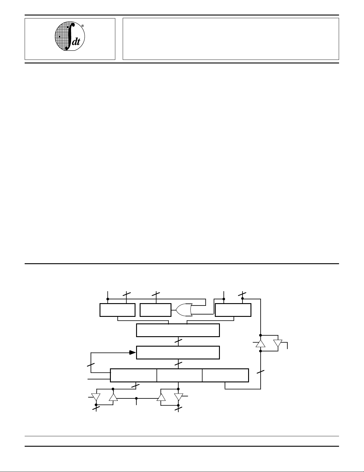
FUNCTIONAL BLOCK DIAGRAM
16
3
PREL
ACC, SUB,
416
CONTROL
REGISTER
MULTIPLIER ARRAY
ACCUMULATOR
MSP REGISTER LSP REGISTERXTP REGISTER
MSP
(P31-P16)
IDT7210
32
35
16
+
TSM
OUT
YREGISTER
IN
Y
(Y15-Y0/P15-P0)
TSL
16
2577 drw 01
PREL
1
IN
X
CLKX CLKYRND, TC
35
CLKP
TSX
3
XTPOUT
(P34-P32)
(X15-X0)
XREGISTER
+/–
MILITARY AND COMMERCIAL TEMPERATURE RANGES AUGUST 1995
1995 Integrated Device Technology, Inc. 11.2 DSC-2018/7
IDT7210L
16 x 16 PARALLEL CMOS MULTIPLIER-ACCUMULATOR MILITARY AND COMMERCIAL TEMPERATURE RANGES
DESCRIPTION (Continued)
The Accumulate input (ACC) enables the device to perform
either a multiply or a multiply-accumulate function. In the
multiply-accumulate mode, output data can be added to or
subtracted from previous results. When the Subtraction (SUB)
input is active simultaneously with an active ACC, a subtraction
can be performed. The double precision accumulated result is
rounded down to either a single precision or single precision
plus 3-bit extended result. In the multiply mode, the Extended
Product output (XTP) is sign extended in the two’s complement
mode or set to zero in the unsigned mode. The Round (RND)
control rounds up the Most Significant Product (MSP) and the
3-bit Extended Product (XTP) outputs. When Preload input
(PREL) is active, all the output buffers are forced into a highimpedance state (see Preload truth table) and external data
can be loaded into the output register by using the TSX, TSL
and TSM signals as input controls.
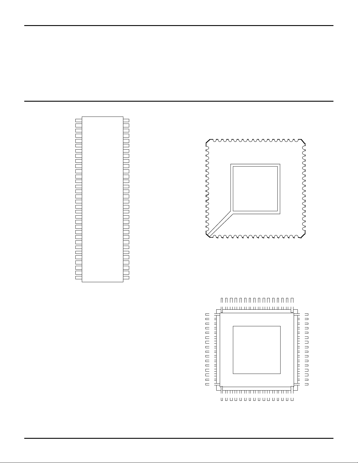
PIN CONFIGURATIONS
X
6
X
X
X
X
X
X
P
P
P
P
P
P
P
P
GND
P
P
10
P
P
11
P
12
P
13
P
14
P15,
P
16
P
17
P
18
P
19
P
20
P
21
P
22
P
23
1
5
2
4
3
3
4
2
5
1
6
0
7
0
,
8
1
,
9
2
,
10
3
,
11
4
,
12
13
5
,
14
6
,
7
,
15
16
17
18
19
20
21
22
23
C64-2
8
,
9
,
,
,
,
,
,
24
25
26
27
28
29
30
31
32
64
63
62
61
60
59
58
57
56
55
54
53
52
51
50
49
48
47
46
45
44
43
42
41
40
39
38
37
36
35
34
33
7
X
X
8
X
9
X
10
X
11
X
12
X
13
X
14
15
X
TSL
RND
SUB
ACC
CLKX
CLKY
CC
V
TC
TSX
PREL
TSM
CLKP
P
34
P
33
P
32
P
31
P
30
P
29
P
28
P
27
P
26
P
25
P
24
P1, Y1
P0, Y0
X0
X1
X2
X3
X4
X5
X6
X7
X8
X9
X10
X11
X12
X13
X14
7, Y7
P
P5, Y5
P4, Y4
P3, Y3
P2, Y2
6059 585756 5554 53 52515049484746 4544
61
62
63
64
65
66
67
68
1
2
3
4
5
6
7
8
9
1011121314 151617 1819 2021 2425 26
15
X
TSL
SUB
RND
P6, Y6
J68-1, L68-1
ACC
CLKX
GND
GND
J68-1
CC
V
CLKY
VCC
P9, Y9
P8, Y8
VCC
PLCC
TOP VIEW
P10, Y10
VCC
P11, Y11
P12, Y12
2223
TC
TSX
P14, Y14
P13, Y13
TSM
PREL
P16
P15, Y15
P34
CLKP
43
P17
42
P18
41
P19
40
P20
39
P21
38
P22
37
P23
36
P24
35
P25
34
P26
33
P27
32
P28
31
P29
30
P30
29
P31
28
P32
27
P33
2577 drw 03
DIP
TOP VIEW
2577 drw 02
P7, Y7
P6, Y6
F64-1
CLKY
P8, Y8
GND
CC
TC
V
P9, Y9
TSX
P10, Y10
P11, Y11
TSM
PREL
P13, Y13
P12, Y12
34
P
CLKP
P14, Y14
P15, Y15
P16
48
47
P17
46
P18
45
P19
44
P20
43
P21
42
P22
41
P23
40
P24
39
P25
38
P26
37
P27
36
P28
35
P29
34
P30
33
P31
2577 drw 04
P33
P32
P0, Y0
X0
X1
X2
X3
X4
X5
X6
X7
X8
X9
X10
X11
X12
X13
X14
P1, Y1
P3, Y3
P4, Y4
P5, Y5
P2, Y2
64636261 605958575655 545352 515049
1
2
3
4
5
6
7
8
9
10
11
12
13
14
15
16
17181920 212223242526 272829 303132
X15
TSL
RND
SUB
ACC
CLKX
FLATPACK
TOP VIEW
11.2 2
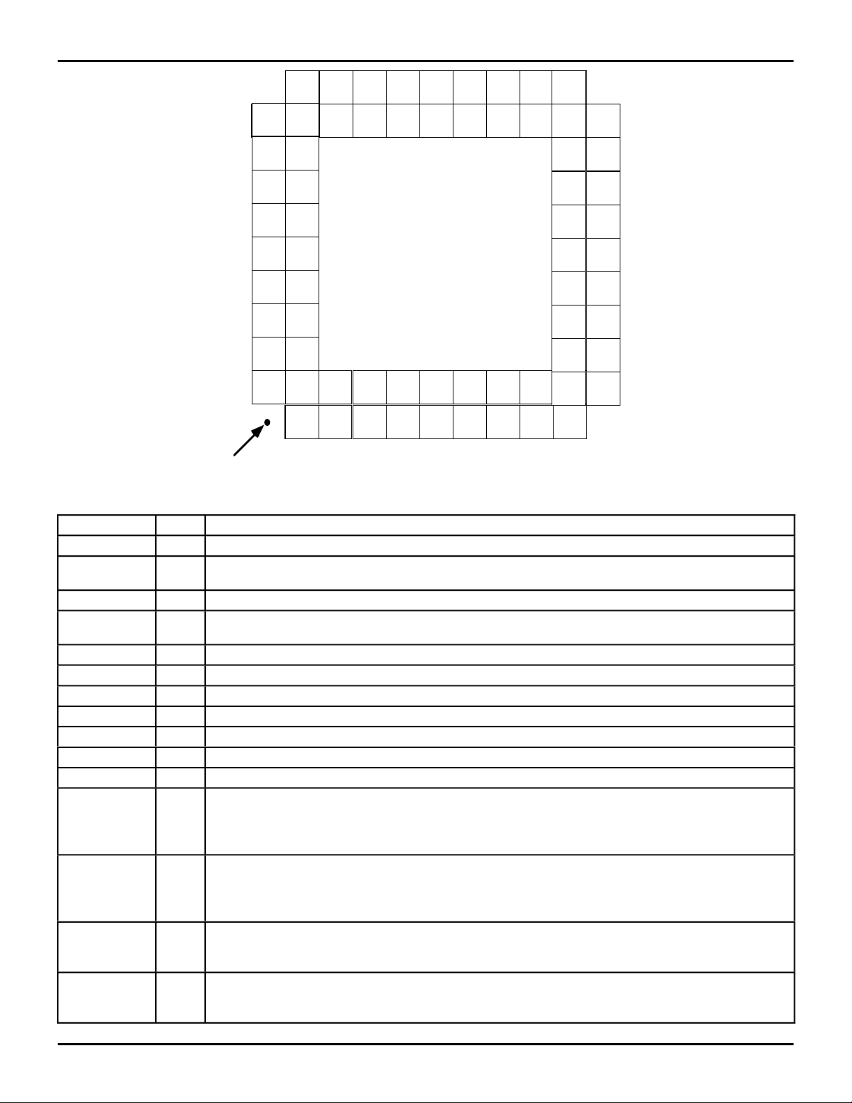
IDT7210L
16 x 16 PARALLEL CMOS MULTIPLIER-ACCUMULATOR MILITARY AND COMMERCIAL TEMPERATURE RANGES
11
10
09
08
07
06
05
04
03
02
01
Pin 1
Designator
NC X15 RND CLKY TC PREL CLKP P33
X14 CLKX VCC TSX P34 NCX13
TSL SUB TSM
X11 X12
X9 X10
X7 X8
X5 X6
X3 X4
X1 X2
Y0,
X0
P0
Y1,P1Y3,P3Y5,P5Y7,
NC
Y2,
Y4,P4Y6,
P2
ABCDEFGHJKL
P6
ACC
G68-2
Y8,P8Y10,
P7
Y9,P9Y11,
GND
PGA
TOP VIEW
P10
P11
Y12,
P12
Y13,
P13
Y14,
P14
Y15,
P15
32
P
P30
P31
P28 P29
P26 P27
P24 P25
P22 P23
P20 P21
P18 P19
P16 P17
NC
2577 drw 05
PIN DESCRIPTIONS
Pin Name I/O Description
X0 - 15 I Data Inputs
Y0 - 15/ P0 - 15 I/O Multiplexed I/O port. Y0 - 15 are data inputs and can be used to preload LSP register on PREL = 1. P0 - 15
are LSP register outputs - enabled by TSL.
P16 - 31 I/O MSP register outputs - enabled by TSM. MSP register can be preloaded when PREL = 1.
P32 - 34 I/O XTP register outputs - enabled by TSX. XTP register can be preloaded through these inputs when
PREL = 1.
CLKX I Input data X0 - 15 loaded in X input register on CLKX rising edge.
CLKY I Input data Y0 - 15 loaded in Y input register on CLKY rising edge.
CLKP I Output data loaded into output register on rising edge of CLKP.
TSX I TSX = 0 enables XTP outputs, TSX = 1 tristates P32 - 34 lines.
TSM I TSM = 0 enables MSP outputs, TSM = 1 tristates P16 - 31 lines.
TSL I TSL = 0 enables LSP outputs, TSL = 1 tristates P0 - 15 lines.
PREL I When PREL= 1 data is input on P0 - 15 lines. When PREL = 0, inputs on these lines are ignored.
ACC I This input is loaded into the control register on the rising edge of (CLKX + CLKY).
When ACC = 1 and SUB = 0 an accumulate operation is performed. When ACC = 1 and SUB = 1, a
subtract operation is performed. When ACC = 0, the SUB input is a don't care and the device acts as a
simple multipler with no accumulation
SUB I This input is loaded into the control register on the rising edge of (CLKX + CLKY).
This input is active only when ACC = 1. When SUB = 1 the contents of the output register are subtracted
from the result and stored back in the output register. When SUB = 0 the contents of the output register
are added to the result and stored back in the output register
TC I This input is loaded into the control register on the rising edge of (CLKX + CLKY).
When TC = 1, the X and Y input are assumed to be in two's complement form. When TC = 0, X and Y
inputs are assumed to be in unsigned magnitude form
RND I This input is loaded into the control register on the rising edge of (CLKX + CLKY).
RND is inactive when low. RND = 1, adds a "1" to the most significant bit of the LSP, to round MSP and
XTP data
2577 tbl 01
11.2 3
 Loading...