

Integrated Device Technology Inc IDT7208L20J, IDT7208L20P, IDT7208L25J, IDT7208L25P, IDT7208L35J Datasheet
...
Integrated Device Technology, Inc.
CMOS ASYNCHRONOUS FIFO
65,536 x 9
ADVANCED
INFORMATION
IDT7208
FEATURES:
• 65536 x 9 storage capacity
• High-speed: 15ns access time
• Low power consumption
— Active: 660mW (max.)
— Power-down: 44mW (max.)
• Asynchronous and simultaneous read and write
• Fully expandable in both word depth and width
• Pin and functionally compatible with IDT720x family
• Status Flags: Empty, Half-Full, Full
• Retransmit capability
• High-performance CMOS technology
• Industrial temperature range (-40oC to +85oC) is available, tested to military electrical specifications
DESCRIPTION:
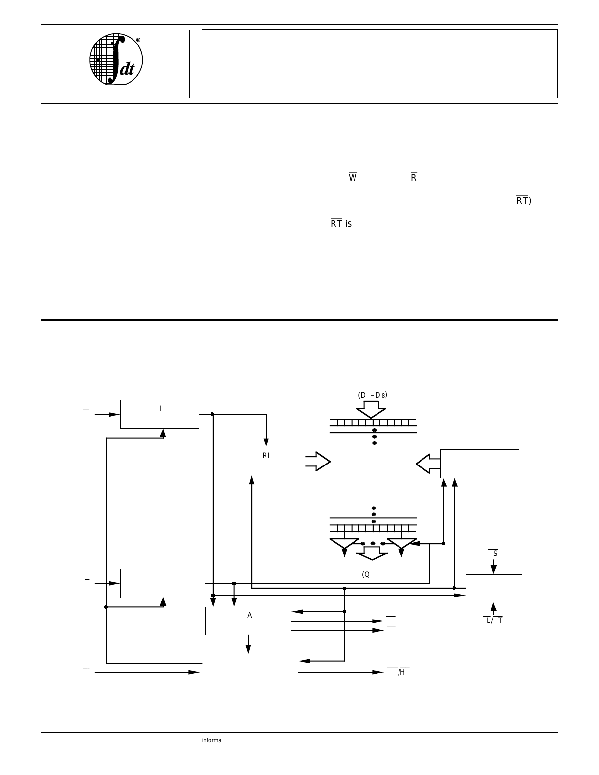
The IDT7208 is a monolithic dual-port memory buffer with
FUNCTIONAL BLOCK DIAGRAM
W
WRITE
CONTROL
•
internal pointers that load and empty data on a first-in/first-out
basis. The device uses Full and Empty flags to prevent data
overflow and underflow and expansion logic to allow for
unlimited expansion capability in both word size and depth.
Data is toggled in and out of the device through the use of
the Write (W) and Read (R) pins.
The device's 9-bit width provides a bit for a control or parity
at the user’s option. It also features a Retransmit (RT) capability that allows the read pointer to be reset to its initial position
when RT is pulsed LOW. A Half-Full Flag is available in the
single device and width expansion modes.
The IDT7208 is fabricated using IDT’s high-speed CMOS
technology. It is designed for applications requiring asynchronous and simultaneous read/writes in multiprocessing, rate
buffering, and other applications.
DATA INPUTS
0
)
(D –D8
RAM ARRAY
65,536 x 9
DATA OUTPUTS
0(Q
)
–Q
8
•
•
EF
FF
XO/HF
•
POINTER
•
READ
RESET
LOGIC
FL/RT
RS
3274 drw 01
R
•
XI
The IDT logo is a registered trademark of Integrated Device Technology, Inc.
READ
CONTROL
•
EXPANSION
•
FLAG
LOGIC
LOGIC
WRITE
POINTER
THREESTATE
BUFFERS
COMMERCIAL TEMPERATURE RANGES DECEMBER 1996
1996 Integrated Device Technology, Inc. DSC-3274/1
For latest information contact IDT's web site at www.idt.com or fax-on-demand at 408-492-8391.
5.06 1
IDT7208 CMOS ASYNCHRONOUS FIFO
65,536 x 9 COMMERCIAL TEMPERATURE RANGES
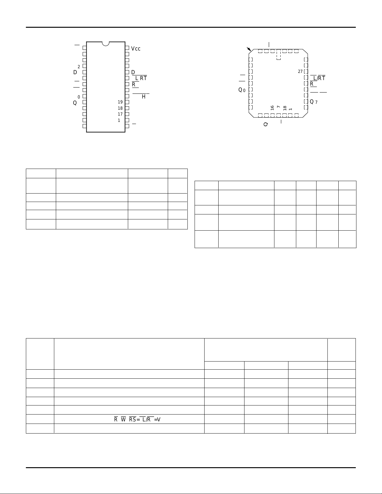
PIN CONFIGURATIONS
1
W
2
D
8
3
D
3
4
2
D
5
D
D
FF
Q
Q
Q
Q
Q
GND
1
0
XI
0
1
2
3
8
6
7
8
9
10
11
12
13
14
P28-1
TOP VIEW
ABSOLUTE MAXIMUM RATINGS
Symbol Rating Commercial Unit
V
TERM Terminal Voltage with –0.5 to + 7.0 V
Respect to GND
T
A Operating Temperature 0 to +70 ° C
T
BIAS Temperature Under Bias –55 to +125 ° C
T
STG Storage Temperature –55 to + 125 ° C
I
OUT DC Output Current 50 mA
NOTE:
1. Stresses greater than those listed under ABSOLUTE MAXIMUM RATINGS may cause permanent damage to the device. This is a stress rating
only and functional operation of the device at these or any other conditions
above those indicated in the operational sections of this specification is not
implied. Exposure to absolute maximum rating conditions for extended
periods may affect reliability.
DIP
28
27
26
25
24
23
22
21
20
19
18
17
16
15
Vcc
D
4
D
5
6
D
D
7
FL/RT
RS
EF
XO/HF
Q
7
Q
6
5
Q
Q
4
R
3274 drw 02
(1)
INDEX
2
D
D
1
D
0
XI
FF
Q
0
Q
1
NC
2
Q
5
6
7
8
9
10
11
12
13
3
8
D
D
432
J32-1
141516
3
8
Q
Q
W
GND
NC
Vcc
32
1
171819
R
NC
4
D5D
30
31
29
6
D
28
D
7
27
NC
26
FL/RT
25
RS
24
EF
23
XO/HF
22
Q
7
21
Q
6
20
5
4
Q
Q
3274 drw 03
PLCC
TOP VIEW
RECOMMENDED DC OPERATING
CONDITIONS
Symbol Parameter Min. Typ. Max. Unit
V
CCC Commercial Supply 4.5 5.0 5.5 V
Voltage
GND Supply Voltage 0 0 0 V
(1)
V
IH
V
IL
NOTE:
1. 1.5V undershoots are allowed for 10ns once per cycle.
Input High Voltage 2.0 — — V
Commercial
(1)
Input Low Voltage — — 0.8 V
Commercial
DC ELECTRICAL CHARACTERISTICS FOR THE 7208
(Commercial: VCC = 5.0V±10%, TA = 0°C to +70°C)
IDT7208
Commercial
t
A = 20, 25, 35 ns
Symbol Parameter Min. Typ. Max. Unit
(1)
LI
I
(2)
LO
I
OH Output Logic “1” Voltage IOH = –2mA 2.4 — — V
V
OL Output Logic “0” Voltage IOL = 8mA — — 0.4 V
V
(3)
CC1
I
(3)
CC2
I
(3)
CC3(L)
I
NOTES:
1. Measurements with 0.4 ≤ V
2. R ≥ V
3. I
4. Tested at f = 20MHz.
IH, 0.4 ≤ VOUT ≤ VCC.
CC measurements are made with outputs open (only capacitive loading).
Input Leakage Current (Any Input) –1 — 1 µA
Output Leakage Current –10 — 10 µA
Active Power Supply Current — — 120
(4)
Standby Current (R=W=RS=FL/RT=VIH)——12mA
Power Down Current (All Input = VCC - 0.2V) — — 8 mA
IN ≤ VCC.
5.06 2
mA
IDT7208 CMOS ASYNCHRONOUS FIFO
65,536 x 9 COMMERCIAL TEMPERATURE RANGES
AC ELECTRICAL CHARACTERISTICS
(1)
(Commercial: VCC = 5V ± 10%, TA = 0°C to +70°C)
Commercial
7208L20 7208L25 7208L35
Symbol Parameters Min. Max. Min. Max. Min. Max. Unit
f
S Shift Frequency — 33.3 — 28.5 — 22.2 MHz
t
RC Read Cycle Time 30 — 35 — 45 — ns
t
A Access Time — 20 — 25 — 35 ns
t
RR Read Recovery Time 10 — 10 — 10 — ns
t
RPW Read Pulse Width
t
RLZ Read LOW to Data Bus LOW
t
WLZ Write HIGH to Data Bus Low-Z
t
DV Data Valid from Read HIGH 5 — 5 — 5 — ns
t
RHZ Read HIGH to Data Bus High-Z
t
WC Write Cycle Time 30 — 35 — 45 — ns
t
WPW Write Pulse Width
t
WR Write Recovery Time 10 — 10 — 10 — ns
t
DS Data Set-up Time 12 — 15 — 18 — ns
t
DH Data Hold Time 0 — 0 — 0 — ns
t
RSC Reset Cycle Time 30 — 35 — 45 — ns
t
RS Reset Pulse Width
t
RSS Reset Set-up Time
t
RTR Reset Recovery Time 10 — 10 — 10 — ns
t
RTC Retransmit Cycle Time 30 — 35 — 45 — ns
t
RT Retransmit Pulse Width
t
RTS Retransmit Set-up Time
t
RSR Retransmit Recovery Time 10 — 10 — 10 — ns
t
EFL Reset to
t
HFH, tFFH Reset to
t
RTF Retransmit LOW to Flags Valid — 30 — 35 — 45 ns
t
REF Read LOW to
t
RFF Read HIGH to
t
RPE Read Pulse Width after
t
WEF Write HIGH to
t
WFF Write LOW to
t
WHF Write LOW to
t
RHF Read HIGH to
t
WPF Write Pulse Width after
t
XOL Read/Write LOW to
t
XOH Read/Write HIGH to
t
XI
t
XIR
t
XIS
XI
XI
XI
EF
HF
Pulse Width
Recovery Time 10 — 10 — 10 — ns
Set-up Time 10 — 10 — 15 — ns
(2)
(3)
(3, 4)
(3)
(2)
(2)
(3)
(2)
(3)
20 — 25 — 35 — ns
5 — 5— 5— ns
5 — 5 — 10 — ns
— 15 — 18 — 20 ns
20 — 25 — 35 — ns
20 — 25 — 35 — ns
20 — 25 — 35 — ns
20 — 25 — 35 — ns
20 — 25 — 35 — ns
LOW — 30 — 35 — 45 ns
and FF HIGH — 30 — 35 — 45 ns
EF
LOW — 20 — 25 — 30 ns
FF
HIGH — 20 — 25 — 30 ns
EF
HIGH 20 — 25 — 35 — ns
EF
HIGH — 20 — 25 — 30 ns
FF
LOW — 20 — 25 — 30 ns
HF
Flag LOW — 30 — 35 — 45 ns
HF
Flag HIGH — 30 — 35 — 45 ns
FF
HIGH 20 — 25 — 35 — ns
XO
LOW — 20 — 25 — 35 ns
XO
HIGH — 20 — 25 — 35 ns
(2)
20 — 25 — 35 — ns
NOTES:
1. Timings referenced as in AC Test Conditions.
2. Pulse widths less than minimum are not allowed.
3. Values guaranteed by design, not currently tested.
4. Only applies to read data flow-through mode.
5.06 3
IDT7208 CMOS ASYNCHRONOUS FIFO
65,536 x 9 COMMERCIAL TEMPERATURE RANGES
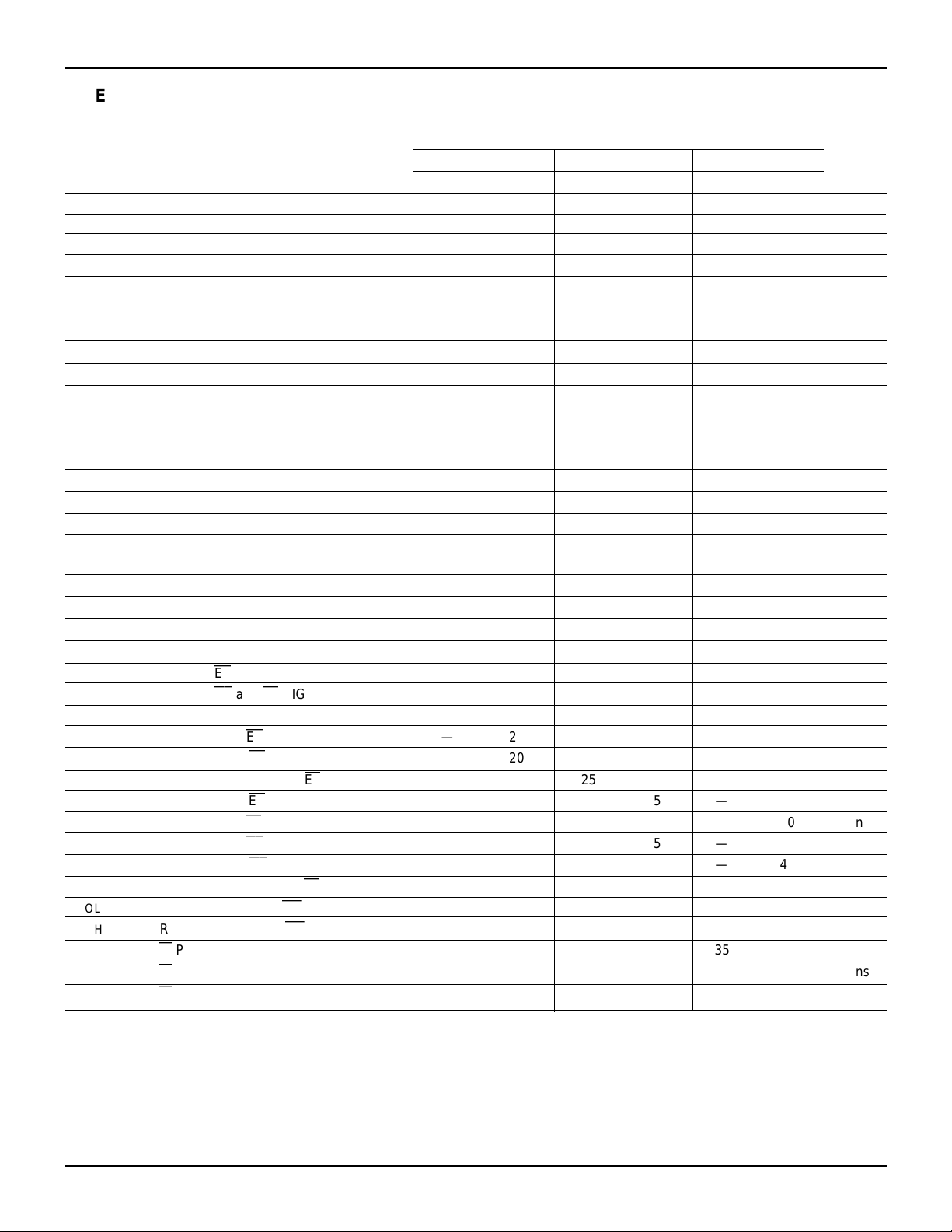
AC TEST CONDITIONS
Input Pulse Levels
Input Rise/Fall Times
Input Timing Reference Levels
Output Reference Levels
Output Load
(1)
CAPACITANCE
Symbol Parameter Condition Max. Unit
(1)
C
IN
C
OUT
NOTES:
1. This parameter is sampled and not 100% tested.
2. With output deselected.
Input Capacitance VIN = 0V 10 pF
(1,2)
Output Capacitance VOUT = 0V 10 pF
(TA = +25°C, f = 1.0 MHz)
GND to 3.0V
5ns
1.5V
1.5V
See Figure 1
SIGNAL DESCRIPTIONS
Inputs:
DATA IN (D0–D8) — Data inputs for 9-bit wide data.
Controls:
RESET (
(RS) input is taken to a LOW state. During reset, both internal
read and write pointers are set to the first location. A reset is
required after power-up before a write operation can take place.
Both the Read Enable (
be in the HIGH state during the window shown in Figure 2
(i.e. tRSS before the rising edge of
change until tRSR after the rising edge of
WRITE ENABLE (
edge of this input if the Full Flag (FF) is not set. Data set-up and
hold times must be adhered-to, with respect to the rising edge
of the Write Enable (W). Data is stored in the RAM array
sequentially and independently of any on-going read operation.
After half of the memory is filled, and at the falling edge of the
next write operation, the Half-Full Flag (HF) will be set to LOW,
and will remain set until the difference between the write pointer
and read pointer is less-than or equal to one-half of the total
memory of the device. The Half-Full Flag (HF) is reset by the
rising edge of the read operation.
To prevent data overflow, the Full Flag (FF) will go LOW on
the falling edge of the last write signal, which inhibits further write
operations. Upon the completion of a valid read operation, the
Full Flag (FF) will go HIGH after t
to begin. When the FIFO is full, the internal write pointer is
blocked from W, so external changes in W will not affect the FIFO
when it is full.
RSRS) — Reset is accomplished whenever the Reset
RR) and Write Enable (
WW) inputs must
RSRS) and should not
RSRS.
WW) — A write cycle is initiated on the falling
RFF, allowing a new valid write
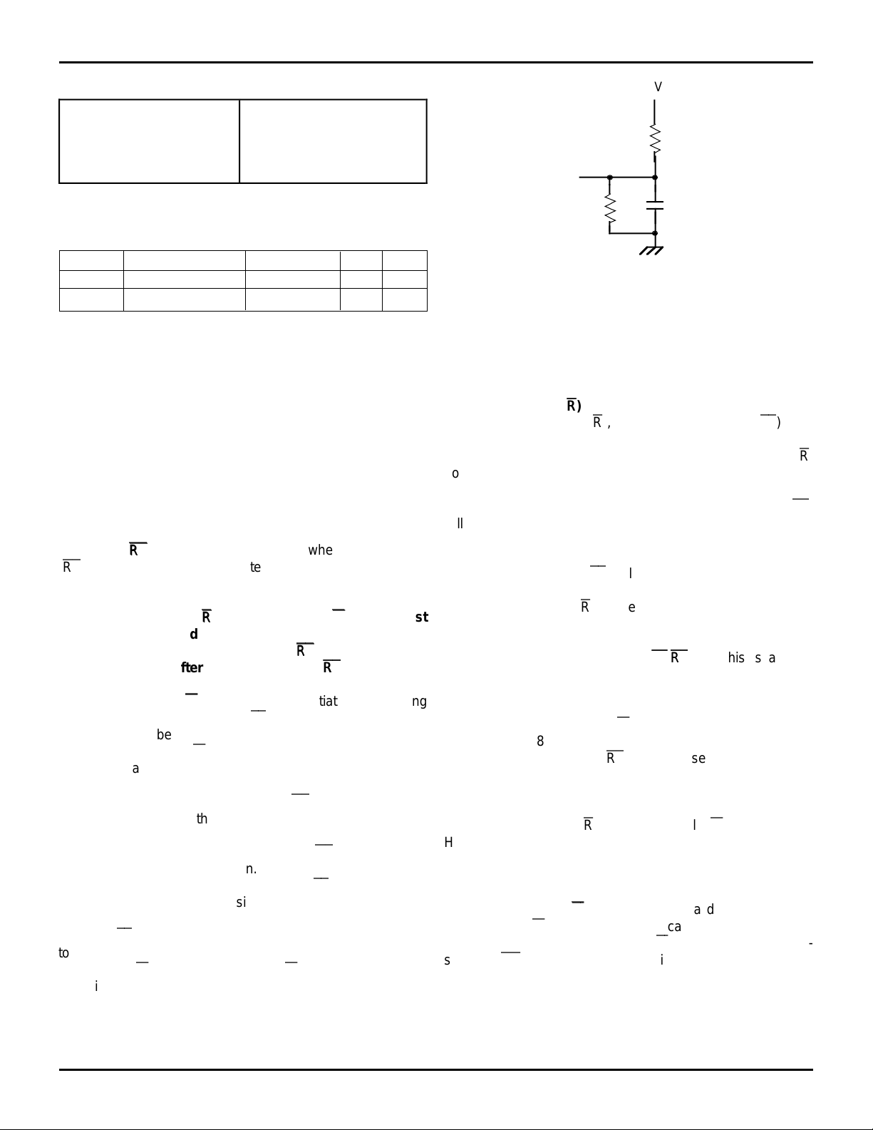
5V
1.1K
Ω
D.U.T.
30pF*
3274 drw 04
*Includes jig and scope capacitances.
READ ENABLE (
Ω
680
OR EQUIVALENT CIRCUIT
Figure 1. Output Load
RR) — A read cycle is initiated on the falling
edge of the Read Enable (R), provided the Empty Flag (EF) is not
set. The data is accessed on a First-In/First-Out basis, independent of any ongoing write operations. After Read Enable (R)
goes HIGH, the Data Outputs (Q0 through Q8) will return to a
high-impedance condition until the next Read operation. When
all the data has been read from the FIFO, the Empty Flag (EF)
will go LOW, allowing the “final” read cycle but inhibiting further
read operations, with the data outputs remaining in a highimpedance state. Once a valid write operation has been accomplished, the Empty Flag (EF) will go HIGH after t
WEF and a valid
Read can then begin. When the FIFO is empty, the internal read
pointer is blocked from R so external changes will not affect the
FIFO when it is empty.
FIRST LOAD/RETRANSMIT (
FLFL/
RTRT) — This is a dual-
purpose input. In the Depth Expansion Mode, this pin is
grounded to indicate that it is the first device loaded (see
Operating Modes). The Single Device Mode is initiated by
grounding the Expansion In (XI).
The IDT7208 can be made to retransmit data when the
Retransmit Enable Control (RT) input is pulsed LOW. A retransmit operation will set the internal read pointer to the first location
and will not affect the write pointer. The status of the Flags will
change depending on the relative locations of the read and write
pointers. Read Enable (R) and Write Enable (W) must be in the
HIGH state during retransmit. This feature is useful when less
than 65,536 writes are performed between resets. The retransmit feature is not compatible with the Depth Expansion Mode.
EXPANSION IN (
XIXI) — This input is a dual-purpose pin.
Expansion In (XI) is grounded to indicate an operation in the
single device mode. Expansion In (XI) is connected to Expansion Out (XO) of the previous device in the Depth Expansion or
Daisy-Chain Mode.
5.06 4
 Loading...