

IDT IDT707278S-L User Manual
HIGH-SPEED
32K x 16 BANK-SWITCHABLE
DUAL-PORTED SRAM WITH
EXTERNAL BANK SELECTS
Features
◆◆
◆
◆◆
32K x 16 Bank-Switchable Dual-Ported SRAM Architecture
– Four independent 8K x 16 banks
– 512 Kilobit of memory on chip
◆◆
◆
◆◆
Fast asynchronous address-to-data access time: 15ns
◆◆
◆
◆◆
User-controlled input pins included for bank selects
◆◆
◆
◆◆
Independent port controls with asynchronous address &
data busses
◆◆
◆
◆◆
Four 16-bit mailboxes available to each port for interprocessor communications; interrupt option
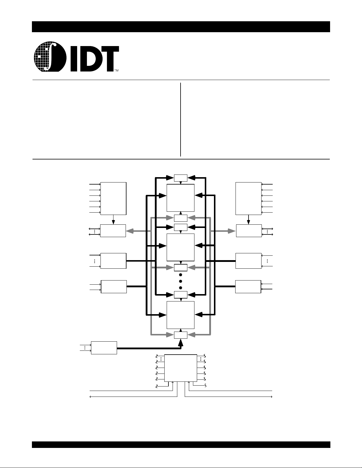
Functional Block Diagram
IDT707278S/L
◆◆
◆
◆◆
Interrupt flags with programmable masking
◆◆
◆
◆◆
Dual Chip Enables allow for depth expansion without
external logic
◆◆
◆
◆◆
UB and LB are available for x8 or x16 bus matching
◆◆
◆
◆◆
TTL-compatible, single 5V (±10%) power supply
◆◆
◆
◆◆
Available in a 100-pin Thin Quad Flatpack (14mm x 14mm)
L
R/
CE
CE
W
UBL
LBL
OE
0L
1L
CONTROL
LOGIC
8Kx16
MEMORY
ARRAY
CONTROL
LOGIC
(BANK 0)
L
W
R/
CE0R
CE
UB
R
LB
OER
R
1R
R
MUX
MUX
I/O
I/O
8L-15L
0L-7L
I/O
CONTROL
MUX
8Kx16
I/O
CONTROL
I/O
I/O
8R-15R
0R-7R
MEMORY
ARRAY
12L
A
(1)
0L
A
BA
1L
0L
BA
ADDRESS
DECODE
BANK
DECODE
(BANK 1)
MUX
MUX
ADDRESS
DECODE
BANK
DECODE
A
A
BA
BA
12R
0R
(1)
1R
0R
8Kx16
MEMORY
ARRAY
(BANK 3)
MUX
(2)
3
BKSEL
BKSEL
(2)
0
MBSELL
INTL
BANK
SELECT
LB
A
A
L
R/
5L
0L
/
UB
OEL
CEL
(1)
(1)
L
MAILBOX
INTERRUPT
LOGIC
L
W
5R
A
0R
A
LBR
OER
R/
(1)
(1)
/
UB
R
R
W
CER
MBSELR
R
INT
NOTES:
1. The first six address pins for each port serve dual functions. When MBSEL = VIH, the pins serve as memory address inputs. When MBSEL = VIL, the pins
serve as mailbox address inputs.
2. Each bank has an input pin assigned that allows the user to toggle the assignment of that bank between the two ports. Refer to Truth Table I for
more details.
MAY 2000
1
©2000 Integrated Device Technology, Inc.
DSC 3739/6
3739 drw 01

IDT707278S/L
32K x 16 Bank-Switchable Dual-Ported SRAM with External Bank Selects Industrial and Commercial Temperature Ranges
Description
The IDT707278 is a high-speed 32K x 16 (512K bit) Bank-Switchable
Dual-Ported SRAM organized into four independent 8K x 16 banks. The
device has two independent ports with separate controls, addresses, and
I/O pins for each port, allowing each port to asynchronously access any
8K x 16 memory block not already accessed by the other port. Accesses
by the ports into specific banks are controlled via bank select pin inputs
under the user's control. Mailboxes are provided to allow inter-processor
communications. Interrupts are provided to indicate mailbox writes have
occurred. An automatic power down feature controlled by the chip enables
(CE
0 and CE1) permits the on-chip circuitry of each port to enter a very
low standby power mode and allows fast depth expansion.
The IDT707278 offers a maximum address-to-data access time as fast
as 15ns, and is packaged in a 100-pin Thin Quad Flatpack (TQFP).
Functionality
The IDT707278 is a high-speed asynchronous 32K x 16 BankSwitchable Dual-Ported SRAM, organized in four 8K x 16 banks. The two
ports are permitted independent, simultaneous access into separate banks
within the shared array. There are four user-controlled Bank Select input
pins, and each of these pins is associated with a specific bank within the
memory array. Access to a specific bank is gained by placing the
associated Bank Select pin in the appropriate state: VIH assigns the bank
to the left port, and VIL assigns the bank to the right port (See Truth Table
IV). Once a bank is assigned to a particular port, the port has full access
to read and write within that bank. Each port can be assigned as many
banks within the array as needed, up to and including all four banks.
The IDT707278 provides mailboxes to allow inter-processor communications. Each port has four 16-bit mailbox registers available to which
it can write and read and which the opposite port can read only. These
mailboxes are external to the common SRAM array, and are accessed
by setting MBSEL = VIL while setting CE = VIH. Each mailbox has an
associated interrupt: a port can generate an interrupt to the opposite port
by writing to the upper byte of any one of its four 16-bit mailboxes. The
interrupted port can clear the interrupt by reading the upper byte. This read
will not alter the contents of the mailbox.
If desired, any source of interrupt can be independently masked via
software. Two registers are provided to permit interpretation of interrupts:
the Interrupt Cause Register and the Interrupt Status Register. The
Interrupt Cause Register gives the user a snapshot of what has caused
the interrupt to be generated - the specific mailbox written to. The
information in this register provides post-mask signals: Interrupt sources
that have been masked will not be updated. The Interrupt Status Register
gives the user the status of all bits that could potentially cause an interrupt
regardless of whether they have been masked. Truth Table V gives a
detailed explanation of the use of these registers.
6.42
2
IDT707278S/L
.
32K x 16 Bank-Switchable Dual-Ported SRAM with External Bank Selects Industrial and Commercial Temperature Ranges
A
A
A
A
A
A
LB
UB
CE
CE
Vcc
R/
OE
GND
GND
(1,2,3)
1
L
E
L
L
0
L
L
L
4
3
5
A
A
A
1009998 9796959493929190898887868584838281 8079 7877 76
1
6L
2
7L
3
8L
4
9L
5
10L
6
11L
NC
7
8
NC
9
0
L
10
L
11
0L
12
1L
13
L
14
15
L
W
16
L
17
18
19
15L
20
14L
21
13L
22
12L
23
11L
24
10L
25
26 27 28 29 30 31 32 33 3435 36 37 38 39 40 41 42 43 44 45 46 47 48 49 50
L
L
c
8
9
c
V
O
O
/
/
I
I
1
L
L
L
0
1
2
A
L
7
O
/
I
A
A
A
A
B
B
L
L
L
L
3
4
5
6
O
O
O
O
/
/
/
/
I
I
I
I
L
2
C
1
A
N
TOP VIEW
L
D
2
N
O
/
G
I
L
S
T
K
N
I
B
IDT707278
PN100-1
100-PIN
TQFP
L
L
0
1
O
O
/
/
I
I
2
L
E
R
D
N
G
R
D
S
2
T
K
1
N
N
B
I
A
G
(3)
R
R
R
R
D
0
1
3
2
N
O
O
O
O
/
/
/
/
G
I
I
I
I
R
R
0
1
R
A
A
0
B
A
B
R
R
R
6
5
4
O
O
O
/
/
/
I
I
I
R
R
R
R
R
4
3
1
A
c
c
V
5
2
A
A
A
A
A
6R
75
A
7R
74
A
8R
73
A
9R
72
A
10R
71
A
11R
70
NC
69
NC
68
BKSEL
LB
R
UB
R
0R
CE
CE
1R
MBSEL
GND
R/
R
W
OE
R
GND
GND
I/O
15R
I/O
14R
I/O
13R
I/O
12R
I/O
11R
I/O
10R
3
R
67
66
65
64
63
62
61
60
59
58
57
56
55
54
53
52
51
R
9
O
/
I
3739 drw 02
C
N
R
R
7
8
O
O
/
/
I
I
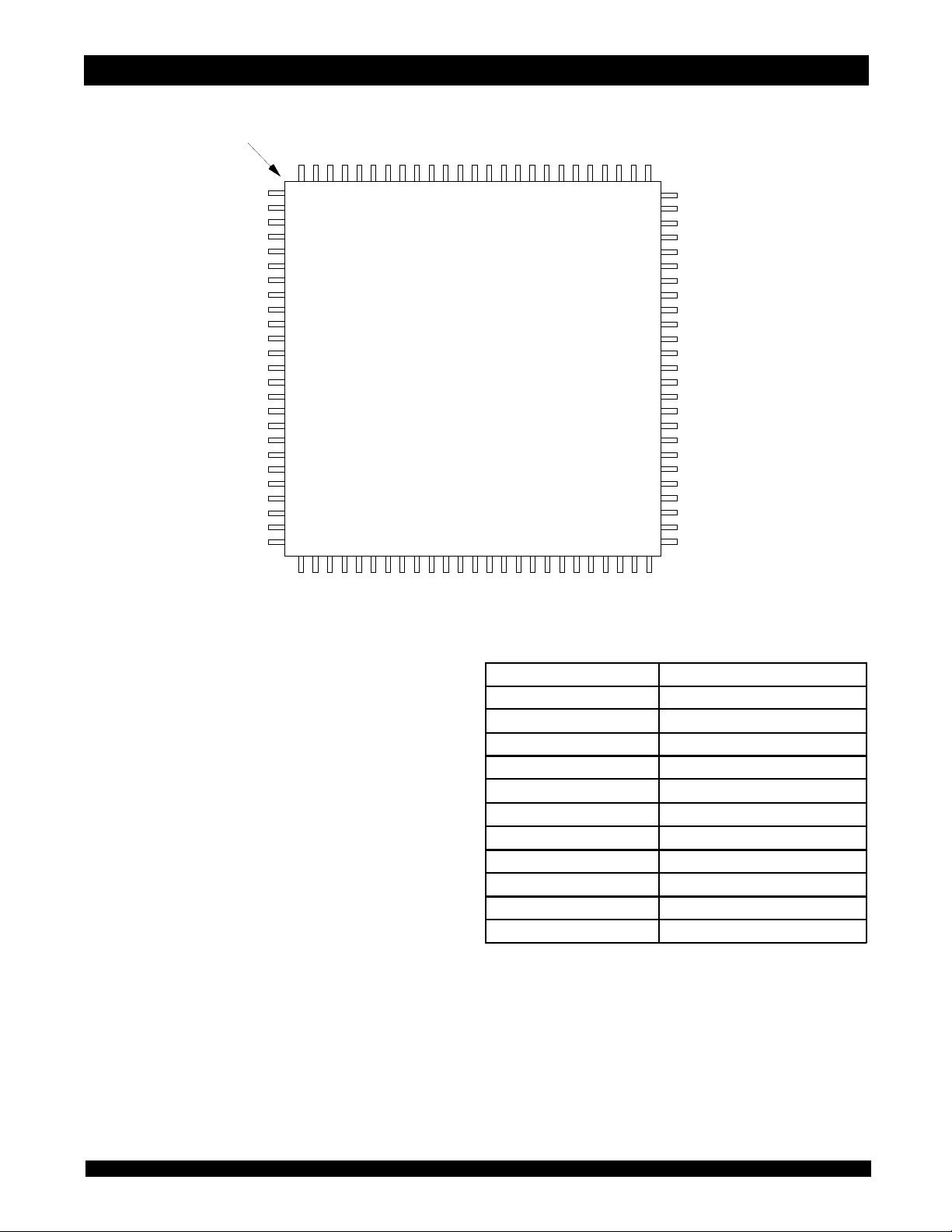
Pin Configurations
INDEX
BKSEL
MBSEL
I/O
I/O
I/O
I/O
I/O
I/O
NOTES:
1. All VCC pins must be connected to power supply.
2. All GND pins must be connected to ground supply.
3. Package body is approximately 14mm x 14mm x 1.4mm.
4. This package code is used to reference the package diagram.
5. This text does not indicate orientation of the actual part-marking.
Pin Names
(1,6)
12
A0 - A
(1)
0
1
- BA
BA
(1)
MBSEL
(2)
0-3
BKSEL
(1)
R/
W
(1)
OE
(1)
0
1
,
CE
CE
(1)
UB, LB
(1)
15
I/O0 - I/O
(1)
INT
(4)
CC
V
(5)
GND
Address Inputs
Bank Address Inputs
Mailbox Access Control Gate
Bank S e le ct Inp uts
Read /Write E nabl e
Output Enab le
Chip E nabl es
I/O Byte Enables
Bi d i re c ti o n al Data Inpu t/ Ou tp ut
Interrupt Flag (Outp ut)
(3)
+5VPower
Ground
NOTES:
1. Duplicated per port.
2. Each bank has an input pin assigned that allows the user to toggle the assignment
of that bank between the two ports. Refer to Truth Table IV for more details. When
changing the bank assignments, accesses of the affected banks must be
suspended. Accesses may continue uninterrupted in banks that are not being
reallocated.
3. Generated upon mailbox access.
4. All Vcc pins must be connected to power supply.
5. All GND pins must be connected to ground supply.
6. The first six address pins (A0-A5) for each port serve dual functions. When
MBSEL = VIH, the pins serve as memory address inputs. When MBSEL = VIL,
the pins serve as mailbox address inputs (A6-A12 ignored).
3739 tbl 01
6.42
3
IDT707278S/L
32K x 16 Bank-Switchable Dual-Ported SRAM with External Bank Selects Industrial and Commercial Temperature Ranges
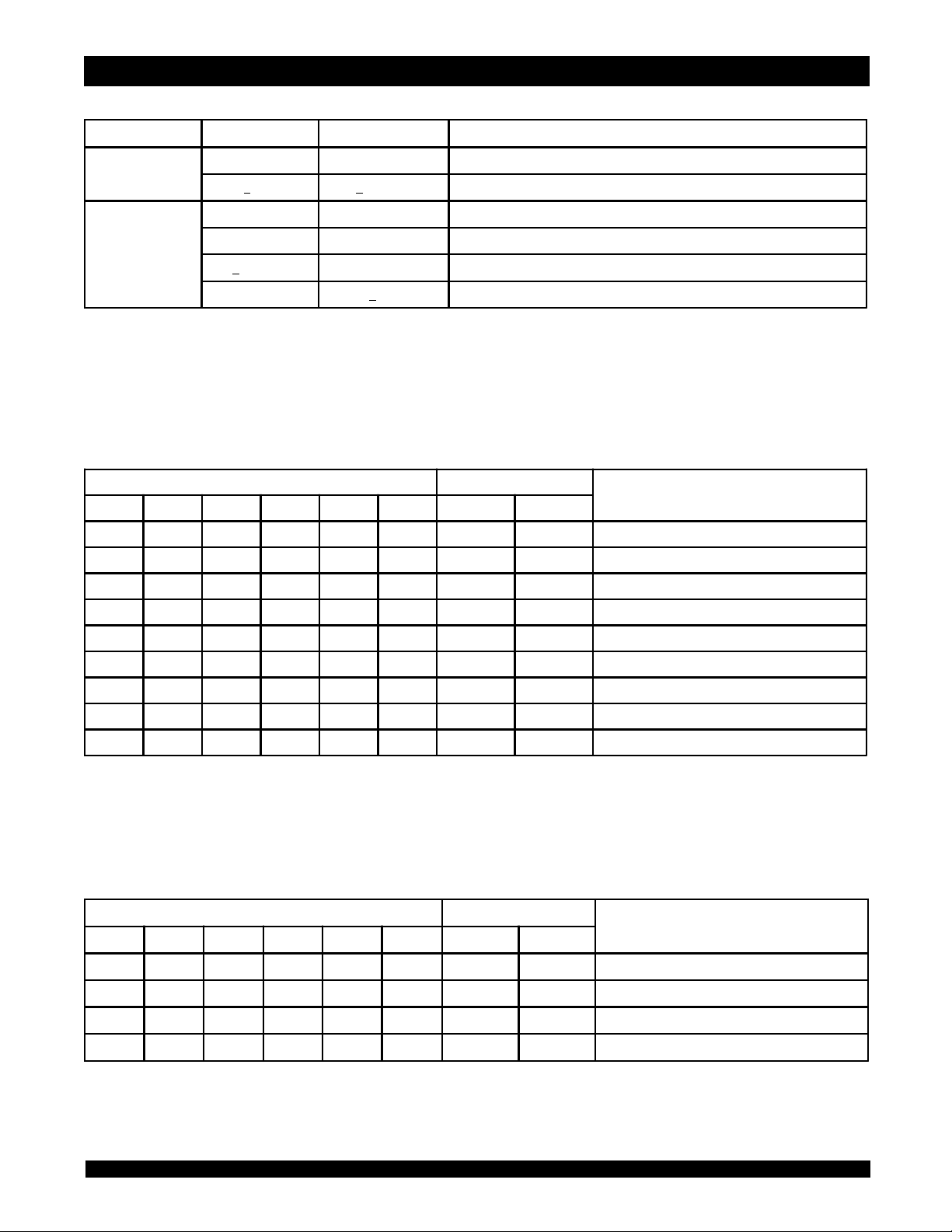
Truth Table I Chip Enable
(1,2,3,4)
CE CE
V
L
< 0.2V >V
V
H
1
0
IL
IH
XV
CE
IH
V
CC
-0.2V Po rt Se le cted (CMOS Ac tive )
Port Selected (TTL Active)
X Port Deselected (TTL Inactive)
IL
Port Deselected (TTL Inactive)
Mode
>VCC -0.2V X P ort De se le cte d (CMOS Inacti ve )
X<
0.2V Port Deselected (CMOS Inactive)
NOTES:
1. Chip Enable references are shown above with the actual CE0 and CE1 levels, CE is a reference only.
2. Port "A" and "B" references are located where CE is used.
3. "H" = VIH and "L" = VIL.
4. CE and MBSEL cannot be active at the same time.
Truth Table II Non-Contention Read/Write Control
(1)
Inputs
CE
(2)
W
R/
OE UB LB MBSEL
H X X X X H Hig h-Z Hig h-Z Des e l cte d : P o we r-Do wn
X
(3)
XXHH X
(3)
LLXLHHDATA
L L X H L H High-Z DAT A
LLXLLHDATA
LHLLHHDATA
LHLHLHHigh-ZDATA
LHLLLHDATA
X
(3)
XHXX X
(3)
NOTES:
1. BA0L - BA1L ¹ BA0R - BA1R: cannot access same bank simultaneously from both ports.
2. Refer to Truth Table I.
3. CE and MBSEL cannot both be active at the same time.
Outputs
I/O
8-15
I/O
0-7
Hig h-Z Hig h-Z Bo th By te s De s e l e cte d
IN
IN
OUT
OUT
High-Z Write to Upper Byte Only
IN
Wri te to Lowe r B y te On ly
IN
DAT A
Wri te to B o th B y te s
High-Z Read Upper Byte Only
OUT
Rea d L owe r B y te O nly
OUT
DAT A
Re ad Bo th By te s
High-Z High-Z Outputs Disabled
3739 tbl 02
Mode
37 39 tb l 03
Truth Table III Mailbox Read/Write Control
(1)
Inputs Outputs
(2)
CE
HHL X
W
R/
OE UB LB MBSEL
(3)
X
(3)
LDATA
HHLLLLDATA
HLX L
(3)
L
(3)
LDATAINDAT A
LXXXXL
8-15
I/O
OUT
OUT
____ ____
I/O
DAT A
DAT A
0-7
OUT
Read Data from Mailbox, ↓ cl ears inte rrup t
OUT
Read Data from Mailbox, ↓ cl ears inte rrup t
IN
Write Data into Mailbo x
Mode
No t All o we d
NOTES:
1. There are four mailbox locations per port written to and read from all the I/O's (I/O0-I/O15). These four mailboxes are addressed by A0-A5. Refer
to Truth Table V.
2. Refer to Truth Table I.
3. Each mailbox location contains a 16-bit word, controllable in bytes by setting input levels to UB and LB appropriately.
6.42
4
3739 t bl 04
IDT707278S/L
32K x 16 Bank-Switchable Dual-Ported SRAM with External Bank Selects Industrial and Commercial Temperature Ranges
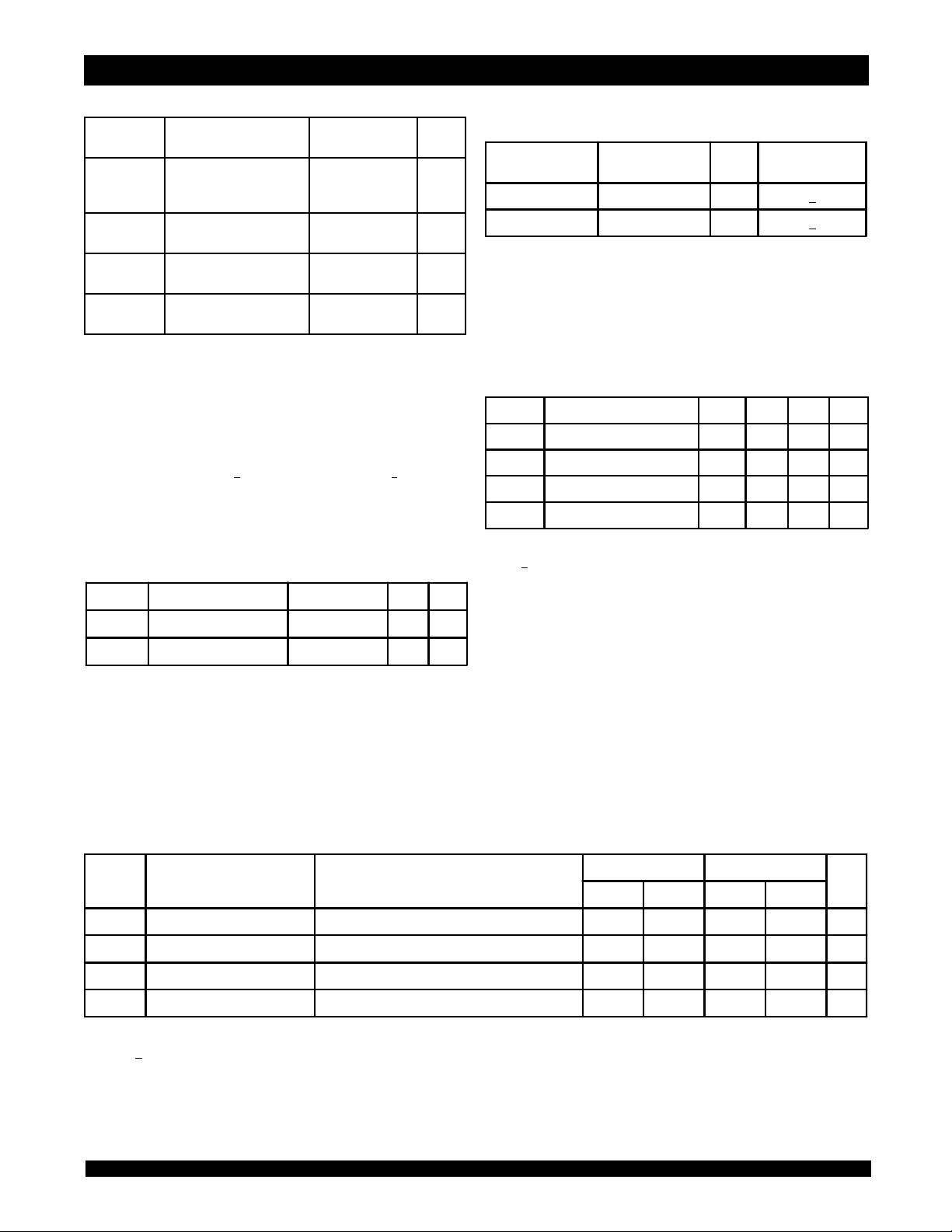
Absolute Maximum Ratings
Symbol Rating Commercial
(2)
TERM
V
T
BIAS
Terminal Voltage
with Re s p e ct
to GND
Tempe rature
(1)
Unit
& Industrial
-0.5 to +7.0 V
-55 to + 125
Maximum Operating
Temperature and Supply Voltage
Grade Ambient
Temperature
O
Commercial 0
o
C
Industrial -40
C to + 70OC0V5.0V + 10%
O
C to + 85OC0V 5.0V + 10%
GND Vcc
Under Bias
STG
T
Storage
-65 to + 150
o
Tempe rature
NOTES:
C
1. This is the parameter TA. This is the "instant on" case temperature.
(1)
3739 t bl 06
OUT
I
DC Outp ut
50 mA
Current
NOTES:
1. Stresses greater than those listed under ABSOLUTE MAXIMUM RATINGS may
cause permanent damage to the device. This is a stress rating only and
functional operation of the device at these or any other conditions above those
indicated in the operational sections of this specification is not implied. Exposure
to absolute maximum rating conditions for extended periods may affect
reliability.
2. VTERM must not exceed Vcc + 10% for more than 25% of the cycle time or 10ns
maximum, and is limited to < 20mA for the period of VTERM > Vcc + 10%.
Capacitance
(1)
3739 tbl 05
(TA = +25°C, f = 1.0MHz) TQFP Package
Symbol Parameter Conditions
Inp ut Cap ac ita nc e VIN = 3dV 9 pF
C
IN
(3)
C
NOTES:
1. This parameter is determined by device characterization but is not production
tested.
2. 3dV represents the interpolated capacitance when the input and output signals
switch from 0V to 3V or from 3V to 0V.
3. COUT represents CI/O as well.
Outp ut Ca p ac itan c e V
OUT
OUT
(2)
Max. Unit
= 3dV 10 pF
3739 tbl 08
Recommended DC Operating
Conditions
Symbol Parameter Min. Typ. Max. Unit
V
Supply Voltage 4.5 5.0 5.5 V
CC
GND Ground 0 0 0 V
IH
Inp ut H ig h Vo ltage 2. 2
V
V
Inp ut L o w Vo l tag e -0. 5
IL
NOTES:
1. VIL > -1.5V for pulse width less than 10ns.
2. VTERM must not exceed Vcc + 10%.
____
(1)
____
(2)
6.0
0.8 V
V
3739 tbl 07
DC Electrical Characteristics Over the Operating
Temperature and Supply Voltage Range
Symbol Parameter Test Conditions
|ILI| Input Leak age Current
LO
| Output Leak age Current
|I
OL
V
Output Low Vo ltage IOL = +4mA
OH
Outp ut Hig h Vo ltag e IOH = -4mA 2.4
V
NOTE:
1. At Vcc < 2.0V, input leakages are undefined.
(1)
VCC = 5. 5V, VIN = 0V to V
IH
= V
MBSE L
,
CE
CC
OUT
= VIH, V
6.42
(VCC = 5.0V ± 10%)
= 0V to V
5
CC
707278S 707278L
___
___
___
10
10
0.4
___
___
___
___
2.4
UnitMin. Max. Min. Max.
5µA
5µA
0.4 V
___
V
3739 tbl 0 9
 Loading...