

Integrated Device Technology Inc IDT6198L20LB, IDT6198L20Y, IDT6198L20YB, IDT6198L25D, IDT6198L25DB Datasheet
...
W
Integrated Device Technology, Inc.
CMOS STATIC RAM
64K (16K x 4-BIT)
with Output Control
IDT6198S
IDT6198L
FEATURES:
• High-speed (equal access and cycle times)
— Military: 20/25/35/45/55/70/85ns (max.)
— Commercial: 15/20/25/35ns (max.)
• Output Enable (OE) pin available for added system flexibility
• Low-power consumption
• JEDEC compatible pinout
• Battery back-up operation—2V data retention (L version
only)
• 24-pin CERDIP, high-density 28-pin leadless chip carrier,
and 24-pin SOJ
• Produced with advanced CMOS technology
• Bidirectional data inputs and outputs
• Military product compliant to MIL-STD-883, Class B
DESCRIPTION:
The IDT6198 is a 65,536-bit high-speed static RAM organized as 16K x 4. It is fabricated using IDT’s high-performance, high-reliability technology—CMOS. This state-of-theart technology, combined with innovative circuit design tech-
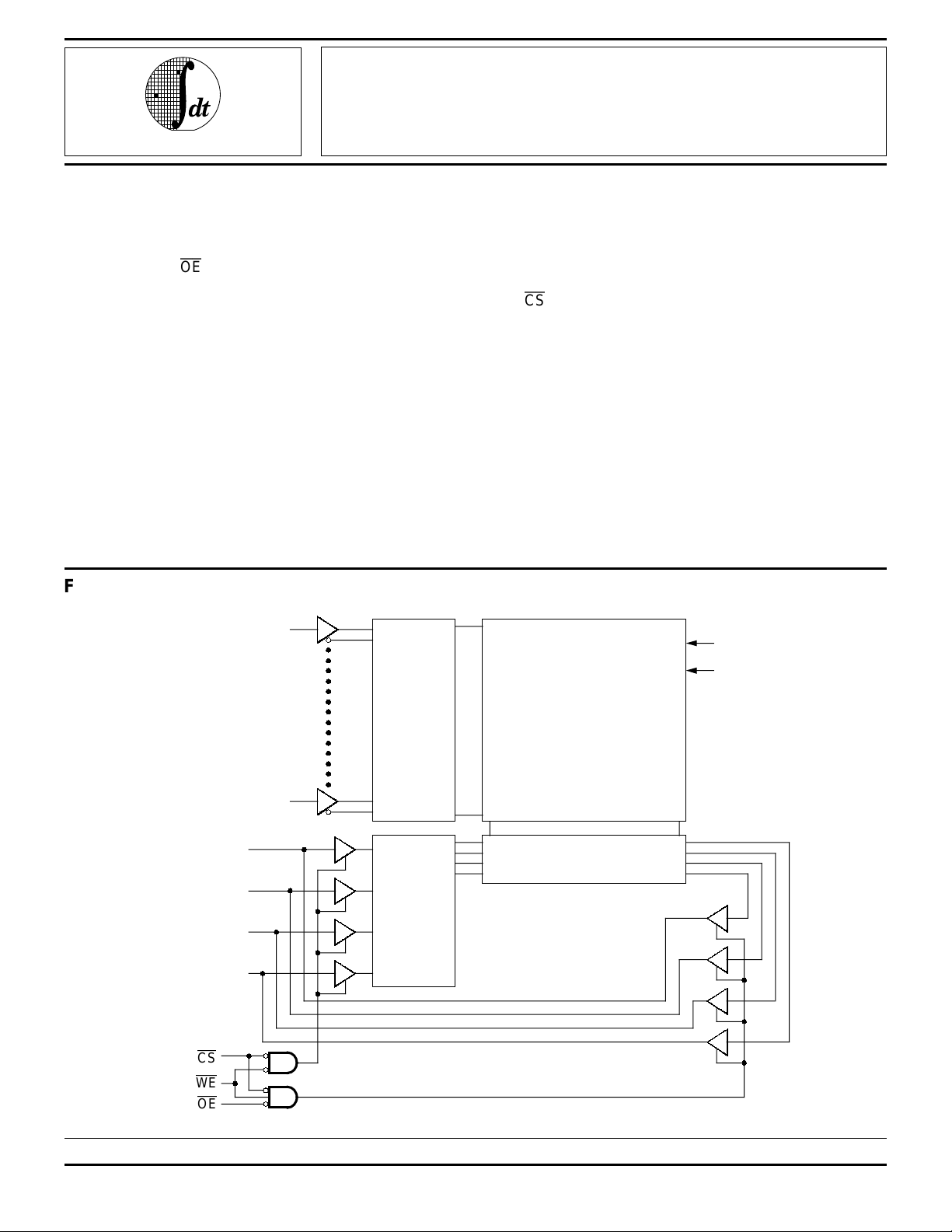
FUNCTIONAL BLOCK DIAGRAM
A0
niques, provides a cost-effective approach for memory intensive applications. Timing parameters have been specified to
meet the speed demands of the IDT79R3000 RISC processors.
Access times as fast as 15ns are available. The IDT6198
offers a reduced power standby mode, I
SB1, which is activated
when CS goes HIGH. This capability significantly decreases
system, while enhancing system reliability. The low-power
version (L) also offers a battery backup data retention capability where the circuit typically consumes only 30µW when
operating from a 2V battery.
All inputs and outputs are TTL-compatible and operate
from a single 5V supply.
The IDT6198 is packaged in either a 24-pin 300 mil CERDIP,
28-pin leadless chip carrier or 24-pin J-bend small outline IC.
Military grade product is manufactured in compliance with
the latest revision of MIL-STD-883, Class B, making it ideally
suited to military temperature applications demanding the
highest level of performance and reliability.
VCC
GND
65,536-BIT
MEMORY ARRAY
COLUMN I/O
2987 drw 01
A13
I/O0
I/O1
I/O2
I/O3
CS
E
OE
The IDT logo is a registered trademark of Integrated Device Technology, Inc.
DECODER
INPUT
DATA
CONTROL
MILITARY AND COMMERCIAL TEMPERATURE RANGES MAY 1994
1994 Integrated Device Technology, Inc. DSC-1010/4
6.3
1
IDT6198S/L
CMOS STATIC RAM 64K (16K x 4-BIT) MILITARY AND COMMERCIAL TEMPERATURE RANGES
PIN CONFIGURATIONS
1
A0
2
A1
3
A2
4
A3
A4
A
A6
A7
A
CS
OE
GND
5
8
5
6
7
8
9
10
11
12
D24-1
&
SO24-4
DIP/SOJ
TOP VIEW
INDEX
1
A
2
A
3
A
4
A
5
A
6
A
7
A
A
8
CS
0
NC
NC
A
32
1
4
5
6
7
L28-2
8
9
10
11
12
13 14 15 16 17
NC
OE
GND
28 27
LCC
TOP VIEW
PIN DESCRIPTIONS
Name Description
A0–A13 Address Inputs
CS
WE
OE
I/O0–I/O3 Data Input/Output
VCC Power
GND Ground
Chip Select
Write Enable
Output Enable
CC
V
WE
24
23
22
21
20
19
18
17
16
15
14
13
2987 drw 02
NC
26
25
24
23
22
21
20
19
18
0
I/O
VCC
A13
A12
A11
A10
A9
NC
I/O3
2
I/O
I/O1
I/O0
WE
NC
A
13
A
12
A
11
A
10
A
9
I/O
3
I/O
2
I/O
1
2987 drw 03
2987 tbl 01
CS
CS
(1)
WE
WE
OE
OE
I/O Power
TRUTH TABLE
Mode
Standby H X X High-Z Standby
Read L H L DATAOUT Active
Write L L X DATAIN Active
Read L H H High-Z Active
NOTE: 2987 tbl 02
1. H = VIH, L = VIL, X = Don't Care
ABSOLUTE MAXIMUM RATINGS
(1)
Symbol Rating Com’l. Mil. Unit
TERM Terminal Voltage –0.5 to +7.0 –0.5 to +7.0 V
V
with Respect
to GND
T
A Operating 0 to +70 –55 to +125 °C
Temperature
BIAS Temperature –55 to +125 –65 to +135 °C
T
Under Bias
STG Storage –55 to +125 –65 to +150 °C
T
Temperature
PT Power Dissipation 1.0 1.0 W
OUT DC Output 50 50 mA
I
Current
NOTE: 2987 tbl 03
1. Stresses greater than those listed under ABSOLUTE MAXIMUM
RATINGS may cause permanent damage to the device. This is a stress
rating only and functional operation of the device at these or any other
conditions above those indicated in the operational sections of this
specification is not implied. Exposure to absolute maximum rating
conditions for extended periods may affect reliability.
CAPACITANCE (TA = +25°C, f = 1.0MHz)
Symbol Parameter
CIN Input Capacitance VIN = 0V 7 pF
C
I/O I/O Capacitance VOUT = 0V 7 pF
NOTE: 2987 tbl 04
1. This parameter is determined by device characterization, but is not
production tested.
(1)
Conditions Max. Unit
6.3 2
IDT6198S/L
CMOS STATIC RAM 64K (16K x 4-BIT) MILITARY AND COMMERCIAL TEMPERATURE RANGES
RECOMMENDED DC OPERATING
CONDITIONS
Symbol Parameter Min. Typ. Max. Unit
VCC Supply Voltage 4.5 5.0 5.5 V
GND Supply Voltage 0 0 0 V
VIH Input High Voltage 2.2 — 6.0 V
IL Input Low Voltage –0.5
V
NOTE: 2987 tbl 05
1. VIL (min.) = –3.0V for pulse width less than 20ns, once per cycle.
(1)
— 0.8 V
RECOMMENDED OPERATING
TEMPERATURE AND SUPPLY VOLTAGE
Grade Temperature GND VCC
Military –55°C to +125°C 0V 5V ± 10%
Commercial 0°C to +70°C 0V 5V ± 10%
2987 tbl 06
DC ELECTRICAL CHARACTERISTICS
VCC = 5.0V ± 10%
IDT6198S IDT6198L
Symbol Parameter Test Condition Min. Max. Min. Max. Unit
LI| Input Leakage Current V CC = Max., MIL. — 10 — 5 µA
|I
VIN = GND to VCC COM’L. — 5 — 2
|I
LO| Output Leakage Current VCC = Max., CS = VIH, MIL. — 10 — 5 µA
VOUT = GND to VCC COM’L. — 5 — 2
OL Output Low Voltage IOL = 10mA, VCC = Min. 0.5 — 0.5 V
V
IOL = 8mA, VCC = Min. — 0.4 — 0.4
V
OH Output High Voltage IOH = –4mA, VCC = Min. 2.4 — 2.4 — V
2987 tbl 07
DC ELECTRICAL CHARACTERISTICS
(1)
(VCC = 5V ± 10%, VLC = 0.2V, VHC = VCC - 0.2V)
6198S15 6198S20 6198S25 6198S35 6198S45 6198S55/70/85
6198L15 6198L20 6198L25 6198L35 6198L45 6198L55/70/85
Symbol Parameter Power Com’l. Mil. Com’l. Mil. Com’l. Mil. Com’l. Mil. Com’l. Mil. Com’l. Mil. Unit
CC1 Operating Power S 100 — 100 105 100 105 100 105 — 105 — 105 mA
I
Supply Current
CS
= V
IL, Outputs Open L 75 — 70 80 70 80 70 80 — 80 — 80
VCC = Max., f = 0
ICC2 Dynamic Operating S 135 — 130 160 125 155 125 140 — 140 — 140 mA
Current
CS
= V
IL, Outputs Open L 125 — 115 130 105 120 105 115 — 110 — 110
VCC = Max., f = fMAX
ISB Standby Power Supply S 60 — 55 70 50 60 45 50 — 50 — 50 mA
Current (TTL Level)
CS
≥ V
IH, VCC = Max., L 45 — 40 50 35 40 30 35 — 35 — 35
Outputs Open, f = fMAX
ISB1 Full Standby Power S 20 — 15 25 15 20 15 20 — 20 — 20 mA
Supply Current (CMOS
Level) CS ≥ V
V
CC=Max., VIN ≥ VHC or
V
IN ≤ VLC, f = 0
NOTES: 2987 tbl 06
1. All values are maximum guaranteed values.
2. At f = f
MAX address and data inputs are cycling at the maximum frequency of read cycles of 1/tRC. f = 0 means no input lines change.
(2)
(2)
(2)
HC, L 1.5 — 0.5 1.5 0.5 1.5 0.5 1.5 — 1.5 — 1.5
(2)
6.3 3
 Loading...