

Integrated Device Technology Inc IDT6178S10Y, IDT6178S12D, IDT6178S12DB, IDT6178S12P, IDT6178S12PB Datasheet
...
IDT6178S
CMOS StaticRAM 16K (4K x 4-BIT) CACHE-TAG RAM MILITARY AND COMMERCIAL TEMPERATURE RANGE
CMOS StaticRAM
IDT6178S
16K (4K x 4-BIT)
CACHE-TAG RAM
Integrated Device Technology, Inc.
FEATURES:
• High-speed Address to MATCH Valid time
– Military: 12/15/20/25ns
– Commercial: 10/12/15/20/25ns (max.)
• High-speed Address Access time
– Military: 12/15/20/25ns
– Commercial: 10/12/15/20/25ns (max.)
• Low-power consumption
– IDT6178S
Active: 300mW (typ.)
• Produced with advanced CMOS high-performance
technology
• Input and output TTL-compatible
• Standard 22-pin Plastic or Ceramic DIP, 24-pin SOJ
• Military product 100% compliant to MIL-STD-883,
Class B
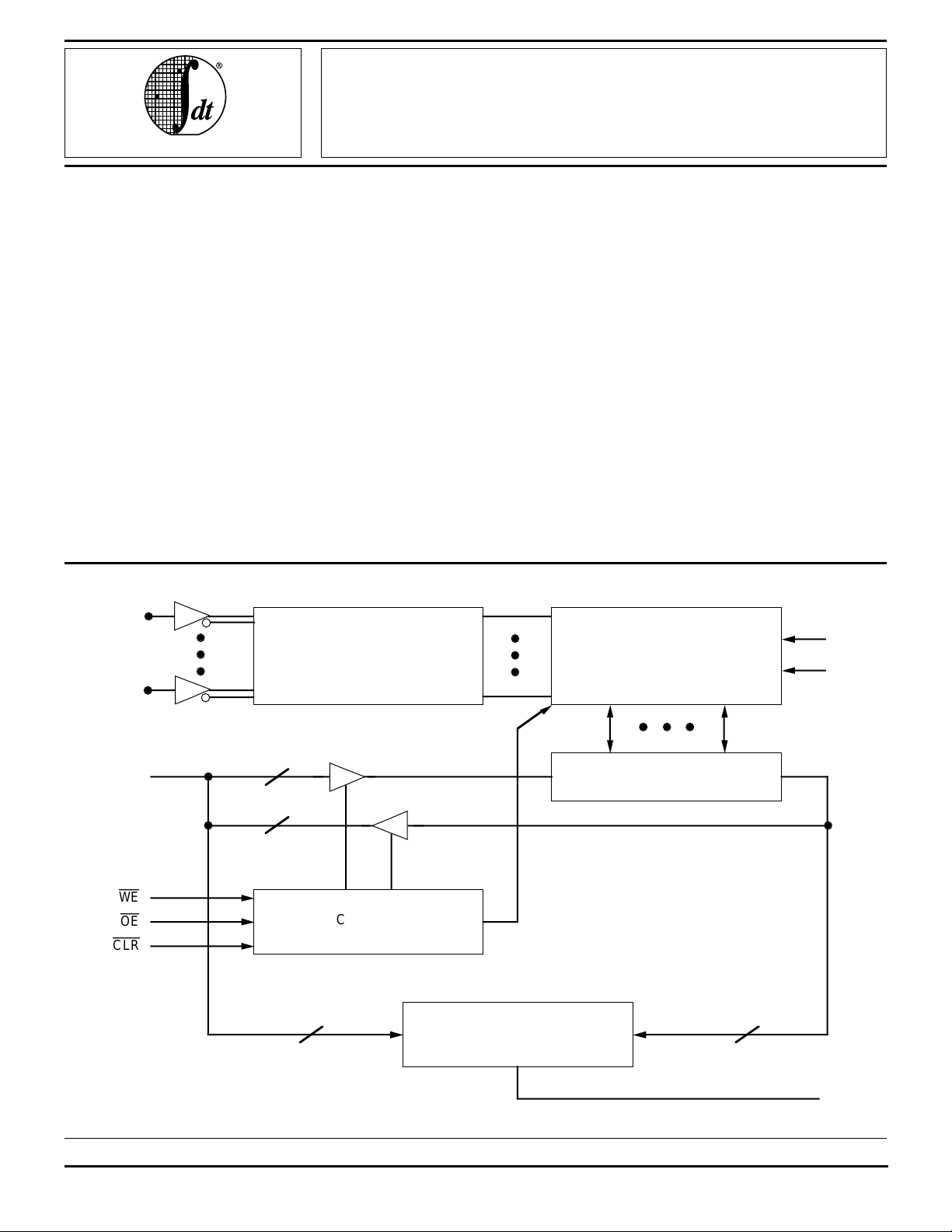
FUNCTIONAL BLOCK DIAGRAM
A0
ADDRESS
DECODE
A11
DESCRIPTION:
The IDT6178 is a high-speed cache address comparator
sub-system consisting of a 16,384-bit StaticRAM organized
as 4K x 4. Cycle Time and Address to MATCH Valid are equal.
The IDT6178 features an onboard 4-bit comparator that
compares RAM contents and current input data. The result is
an active HIGH on the MATCH pin. The MATCH pins of
several IDT6178s can be handed together to provide enabling
or acknowledging signals to the data cache or processor.
The IDT6178 is fabricated using IDT’s high-performance,
high-reliability CMOS technology. Address to MATCH and
Data to MATCH times are as fast as 10ns.
All inputs and outputs of the IDT6178 are TTL-compatible
and the device operates from a single 5V supply.
The IDT6178 is packaged in either a 22-pin, 300-mil Plastic
or Ceramic DIP package or 24-pin SOJ. Military grade product
is manufactured in compliance with latest revision of MILSTD-883, Class B, making it ideally suited to military temperature applications demanding the highest level of performance
and reliability.
16,384-BIT
MEMORY
ARRAY
VCC
GND
0 – I/O3
I/O
WE
OE
CLR
The IDT logo is a registered trademark of Integrated Device Technology, Inc.
4
4
CLEAR
MEMORY
CONTROL
4 4
COMPARATOR
ARRAY
CONTROL I/O
MATCH
2953 drw 01
MILITARY AND COMMERCIAL TEMPERATURE RANGES MAY 1994
1994 Integrated Device Technology, Inc. DSC-1059/2
11.1 1
11.1
1
IDT6178S
CMOS StaticRAM 16K (4K x 4-BIT) CACHE-TAG RAM MILITARY AND COMMERCIAL TEMPERATURE RANGE
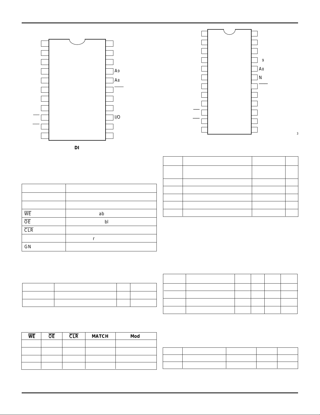
PIN CONFIGURATIONS
A0
A1
A2
A3
A4
A5
A6
A7
OE
WE
GND
1
2
3
4
5
617
P22-1
&
D22-1
7
8
9
10 13
11 12
DIP
TOP VIEW
22
21
20
19
18
16
15
14
PIN DESCRIPTIONS
A0–A11 Address Inputs
I/O0–I/O3 Data Input/Output
MATCH Match
WE
OE
CLR
VCC Power
GND Ground
Write Enable
Output Enable
Clear
V
CC
A11
A10
A9
A8
CLR
I/O
3
I/O
2
I/O1
I/O0
MATCH
2953 drw 02
2953 tbl 01
A
A
A
A
A
A
NC
A
A
OE
WE
GND
0
124
1
223
2
322
3
4
4
5
5
6
7
8
6
9
7
10
11
12
S024-4
21
20
19
18
17
16
15
14
13
CC
V
A
11
A
10
A
9
A
8
NC
CLR
I/O
3
2
I/O
I/O
1
I/O
0
MATCH
2953 drw 03
SOJ
TOP VIEW
ABSOLUTE MAXIMUM RATINGS
(1)
Symbol Rating Value Unit
TERM Terminal Voltage with respect –0.5 to +7.0 V
V
to GND
T
A Operating Temperature –55 to +125 °C
BIAS Temperature Under Bias –65 to +135 °C
T
STG Storage Temperature –65 to +150 °C
T
T Power Dissipation 1.0 W
P
OUT DC Output Current 50 mA
I
NOTE:
1. Stresses greater than those listed under ABSOLUTE MAXIMUM RATINGS
may cause permanent damage to the device. This is a stress rating only
and functional operation of the device at these or any other conditions
above those indicated in the operational sections of this specification is not
implied. Exposure to absolute maximum rating conditions for extended
periods may affect reliabilty.
2953 tbl 04
RECOMMENDED OPERATING
TEMPERATURE AND SUPPLY VOLTAGE
Grade Ambient Temperature GND VCC
Commercial 0°C to +70°C 0V 5.0V ± 10%
Military –55°C to +125°C 0V 5.0V ± 10%
2953 tbl 02
TRUTH TABLES
WE
WE
H H H Valid
L X H Invalid Write Cycle
H L H Invalid Read Cycle
X X L Invalid Clear Cycle
NOTE: 2953 tbl 03
1. H = VIH, L = VIL, X = Don’t care.
2. Valid Match = V
OE
OE
(1)
CLR
CLR
OH, Valid Non-Match = VOL.
MATCH Mode
(2)
Match Cycle
RECOMMENDED DC
OPERATING CONDITIONS
Symbol Parameter Min. Typ. Max. Unit
CC Supply Voltage 4.5 5.0 5.5 V
V
GND Supply Voltage 0 0 0 V
IH Input High Voltage 2.2
V
IL Input Low Voltage –0.5
V
NOTES: 2953 tbl 05
1. VIL = –3.0V for pulse width less than 20ns, once per cycle.
IH = 2.5V for clear pin.
2. V
(2)
– 6.0 V
(1)
– 0.8 V
CAPACITANCE (TA = 25°C, f = 1MHz)
Symbol Parameter Condition Max Units
IN Input Capacitance VIN = 0V 8 pF
C
I/O I/O Capacitance VOUT = 0V 8 pF
C
NOTE: 2953 tbl 06
1. This parameter is determined by device characterization, but is not
production tested.
11.1 2
IDT6178S
CMOS StaticRAM 16K (4K x 4-BIT) CACHE-TAG RAM MILITARY AND COMMERCIAL TEMPERATURE RANGE
DC ELECTRICAL CHARACTERISTICS (VCC = 5.0V ± 10%, All Temperature Ranges)
6178S
Symbol Parameter Test Condition Min. Max. Unit
LI| Input Leakage Current VCC = 5.5V, VIN = 0V to VCC —10µA
|I
LO| Output Leakage Current
|I
OL Output Low Voltage IOL = 8mA (I/O0 – I/O3) — 0.4 V
V
OH Output High Voltage IOH = –4mA (I/O0 – I/O3) 2.4 — V
V
OE
= VIH, VOUT = 0V to VCC —10µA
OL = 10mA (I/O0 – I/O3) — 0.5 V
I
OL = 16mA (Match) — 0.4 V
I
OL = 20mA (Match) — 0.5 V
I
OH = –8mA (Match) 2.4 — V
I
2953 tbl 07
DC ELECTRICAL CHARACTERISTICS (VCC = 5.0V ± 10%, All Temperature Ranges)
6178S10 6178S12
(1)
6178S15
Symbol Parameter Max. Max. Max. Max. Unit
CC1 Operating Power Supply Current COM'L. 90 90 90 90 mA
I
Outputs Open, V
CC2 Dynamic Operating Current COM'L. 180 160 140 140 mA
I
Outputs Open, V
NOTES: 2953 tbl 08
1. Military values are preliminary only.
MAX = 1/tRC, only address inputs are cycling at fMAX. f = 0 means no address inputs change.
2. f
CC
= Max., f = 0
CC = Max., f = fMAX
(2)
MIL. — 110 110 110 mA
(2)
MIL. — 180 160 160 mA
(1)
6178S20/25
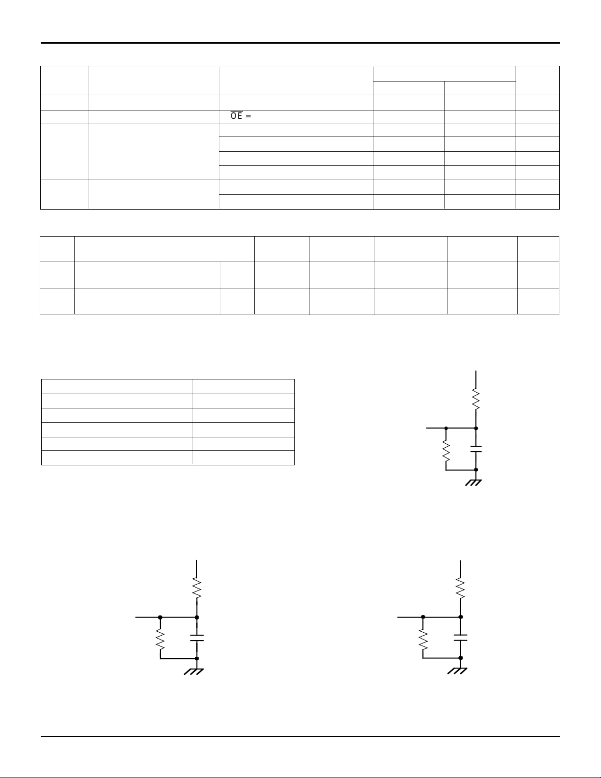
AC TEST CONDITIONS
Input Pulse Levels GND to 3.0V
Input Rise/Fall Times 5ns
Input Timing Reference Levels 1.5V
Output Reference Levels 1.5V
AC Test Load See Figures 2 and 3
AC Test Load for Match Cycle See Figure 1
+5V
480
Ω
DATA
OUT
Ω
30pF*255
2953 tbl 09
+5V
MATCH
OUT
Ω
Figure 1. AC Test Load for MATCH
+5V
480Ω
DATAOUT
5pF*255Ω
240
Ω
30pF*128
2953 drw 04
Figure 2. AC Test Load
2953 drw 05
* Including scope and jig.
11.1 3
2953 drw 06
Figure 3. AC Test Load
(for tOLZ, tOHZ, tWHZ, tOW)
 Loading...