

查询IDT5T9310供应商
IDT5T9310
2.5V LVDS 1:10 CLOCK BUFFER TERABUFFER II
INDUSTRIAL TEMPERATURE RANGE
2.5V LVDS 1:10
CLOCK BUFFER
TERABUFFER™ II
FEA TURES:
• Guaranteed Low Skew < 25ps (max)
• Very low duty cycle distortion < 125ps (max)
• High speed propagation delay < 1.75ns (max)
• Up to 1GHz operation
• Selectable inputs
• Hot insertable and over-voltage tolerant inputs
• 3.3V / 2.5V LVTTL, HSTL, eHSTL, LVEPECL (2.5V), LVPECL (3.3V),
CML, or LVDS input interface
• Selectable differential inputs to ten LVDS outputs
• Power-down mode
• 2.5V VDD
• Available in VFQFPN package
APPLICA TIONS:
• Clock distribution
IDT5T9310
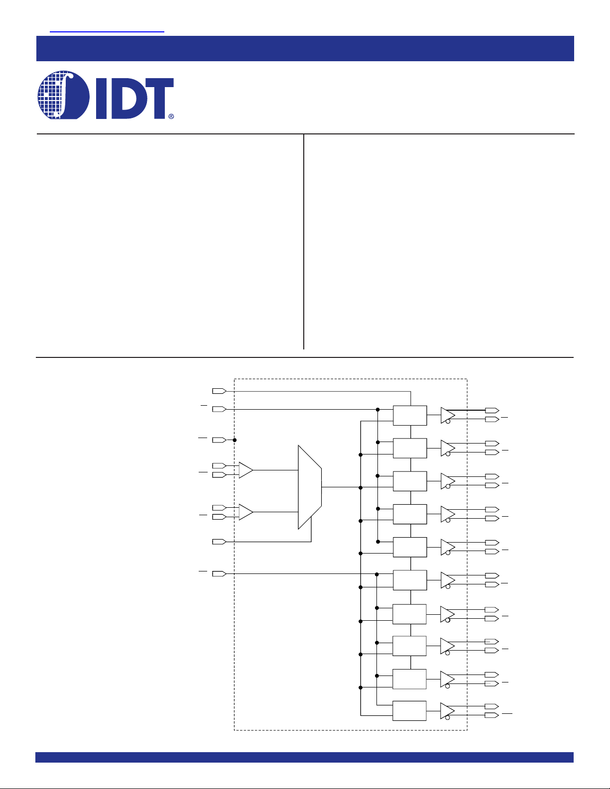
DESCRIPTION:
The IDT5T9310 2.5V differential clock buffer is a user-selectable differential
input to ten LVDS outputs. The fanout from a differential input to ten LVDS outputs
reduces loading on the preceding driver and provides an efficient clock
distribution network. The IDT5T9310 can act as a translator from a differential
HSTL, eHSTL, LVEPECL (2.5V), LVPECL (3.3V), CML, or LVDS input to
LVDS outputs. A single-ended 3.3V / 2.5V LVTTL input can also be used to
translate to LVDS outputs. The redundant input capability allows for an
asynchronous change-over from a primary clock source to a secondary clock
source. Selectable reference inputs are controlled by SEL.
The IDT5T9310 outputs can be asynchronously enabled/disabled. When
disabled, the outputs will drive to the value selected by the GL pin. Multiple power
and grounds reduce noise.
FUNCTIONAL BLOCK DIAGRAM
GL
G1
PD
A1
A1
A2
A2
SEL
G2
OUTPUT
CONTROL
OUTPUT
CONTROL
1
0
OUTPUT
CONTROL
OUTPUT
CONTROL
OUTPUT
CONTROL
OUTPUT
CONTROL
OUTPUT
CONTROL
OUTPUT
CONTROL
Q1
Q1
Q2
Q2
Q3
Q3
Q4
Q4
Q5
Q5
Q6
Q6
Q7
Q7
Q8
Q8
Q9
Q9
Q10
Q10
MARCH 2004
The IDT logo is a registered trademark of Integrated Device Technology, Inc.
INDUSTRIAL TEMPERATURE RANGE
OUTPUT
CONTROL
OUTPUT
CONTROL
1
© 2004 Integrated Device Technology, Inc. DSC-6175/13
IDT5T9310
2.5V LVDS 1:10 CLOCK BUFFER TERABUFFER II
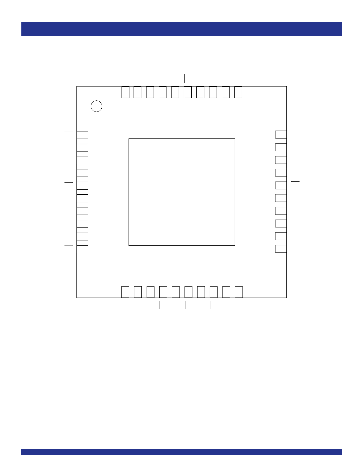
PIN CONFIGURATION
INDUSTRIAL TEMPERATURE RANGE
G1
V
DD
GND
Q1
Q1
Q2
Q2
DD
V
A1
L
E
S
39 38 37 36 35 34 33
40
1
2
3
4
5
0
1
Q
0
1
Q
Q9Q9Q8Q8V
32
D
C
D
N
31
30
29
28
27
26
G
2
PD
VDD
Q7
Q7
D
D
V
GND
6
7
8
9
25
24
23
22
Q6
Q6
VDD
A2
A1
10
L
G
12
13 14 15
D
D
V
1611
4
Q3Q3Q4Q
VFQFPN
TOP VIEW
17 18 19
5Q5
Q
21
A2
20
D
D
D
N
V
G
2

IDT5T9310
2.5V LVDS 1:10 CLOCK BUFFER TERABUFFER II
INDUSTRIAL TEMPERATURE RANGE
ABSOLUTE MAXIMUM RATINGS
(1)
Symbol Description Max Unit
VDD Power Supply Voltage –0.5 to +3.6 V
VI Input Voltage –0.5 to +3.6 V
VO Output Voltage
(2)
–0.5 to VDD +0.5 V
CAPACITANCE
Symbol Parameter Min Typ. Max. Unit
C
IN Input Capacitance —— 3pF
NOTE:
1. This parameter is measured at characterization but not tested
(1)
(TA = +25°C, F = 1.0MHz)
TSTG Storage Temperature –65 to +150 °C
T
J Junction Temperature 150 °C
NOTES:
1. Stresses greater than those listed under ABSOLUTE MAXIMUM RATINGS may cause
permanent damage to the device. This is a stress rating only and functional operation
of the device at these or any other conditions above those indicated in the operational
sections of this specification is not implied. Exposure to absolute maximum rating
conditions for extended periods may affect reliability.
2. Not to exceed 3.6V.
RECOMMENDED OPERATING RANGE
Symbol Description Min. Typ. Max. Unit
TA Ambient Operating Temperature –40 +25 +85 °C
DD Internal Power Supply Voltage 2.3 2. 5 2.7 V
V
PIN DESCRIPTION
Symbol I/O Type Description
A[1:2] I Adjustable
A
[1:2] I Adjustable
1 I LVTTL Gate control for differential outputs Q1 and Q1 through Q5 and Q5. When G1 is LOW, the differential outputs are active. When G1 is
G
2 I LVTTL Gate control for differential outputs Q6 and Q6 through Q10 and Q10. When G2 is LOW, the differential outputs are active. When G2 is
G
GL I LVTTL Specifies output disable level. If HIGH, "true" outputs disable HIGH and "complementary" outputs disable LOW. If LOW, "true"
Qn O LVDS Clock outputs
Qn O LVDS Complementary clock outputs
SEL I LVTTL Reference clock select. When LOW, selects A2 and A2. When HIGH, selects A1 and A1.
PD I LVTTL Power-down control. Shuts off entire chip. If LOW, the device goes into low power mode. Inputs and outputs are disabled. Both
VDD PWR Power supply for the device core and inputs
GND PWR Power supply return for all power
NC No connect; recommended to connect to GND
NOTES:
1. Inputs are capable of translating the following interface standards:
Single-ended 3.3V and 2.5V LVTTL levels
Differential HSTL and eHSTL levels
Differential LVEPECL (2.5V) and LVPECL (3.3V) levels
Differential LVDS levels
Differential CML levels
2. Because the gate controls are asynchronous, runt pulses are possible. It is the user's responsibility to either time the gate control signals to minimize the possibility of runt
pulses or be able to tolerate them in down stream circuitry.
3. It is recommended that the outputs be disabled before entering power-down mode. It is also recommended that the outputs remain disabled until the device completes powerup after asserting PD.
4. The user must take precautions with any differential input interface standard being used in order to prevent instability when there is no input signal.
(1,4)
Clock input. A[1:2] is the "true" side of the differential clock input.
(1,4)
Complementary clock inputs. A[1:2] is the complementary side of A[1:2]. For LVTTL single-ended operation, A[1:2] should be set to the
desired toggle voltage for A[1:2]:
3.3V LVTTL V
REF = 1650mV
2.5V LVTTL VREF = 1250mV
HIGH, the differential outputs are asynchronously driven to the level designated by GL
HIGH, the differential outputs are asynchronously driven to the level designated by GL
(2)
.
(2)
.
outputs disable LOW and "complementary" outputs disable HIGH.
"true" and "complementary" outputs will pull to VDD. Set HIGH for normal operation.
(3)
3

IDT5T9310
2.5V LVDS 1:10 CLOCK BUFFER TERABUFFER II
INDUSTRIAL TEMPERATURE RANGE
DC ELECTRICAL CHARACTERISTICS OVER OPERA TING RANGE FOR LVTTL
Symbol Parameter Test Conditions Min. Typ.
(2)
Max Unit
(1)
Input Characteristics
IIH Input HIGH Current VDD = 2.7V — — ±5 µA
IIL Input LOW Current VDD = 2.7V — — ±5
VIK Clamp Diode Voltage VDD = 2.3V, IIN = -18mA — - 0.7 - 1.2 V
VIN DC Input Voltage - 0.3 — +3.6 V
VIH DC Input HIGH 1.7 — — V
VIL DC Input LOW — — 0.7 V
VTHI DC Input Threshold Crossing Voltage — VDD /2 — V
REF Single-Ended Reference Voltage
V
(3)
3.3V LVTTL — 1.65 — V
2.5V LVTTL — 1.25 —
NOTES:
1. See RECOMMENDED OPERATING RANGE table.
2. Typical values are at VDD = 2.5V, +25°C ambient.
3. For A[1:2] single-ended operation, A[1:2] is tied to a DC reference voltage.
DC ELECTRICAL CHARACTERISTICS OVER OPERA TING RANGE FOR DIFFERENTIAL INPUTS
Symbol Parameter Test Conditions Min. Typ.
Input Characteristics
IIH Input HIGH Current VDD = 2.7V — — ±5 µA
IIL Input LOW Current VDD = 2.7V — — ±5
VIK Clamp Diode Voltage VDD = 2.3V, IIN = -18mA — - 0.7 - 1.2 V
VIN DC Input Voltage - 0.3 — +3.6 V
VDIF DC Differential Voltage
CM DC Common Mode Input Voltage
V
NOTES:
1. See RECOMMENDED OPERATING RANGE table.
2. Typical values are at VDD = 2.5V, +25°C ambient.
3. VDIF specifies the minimum input differential voltage (VTR - VCP) required for switching where VTR is the "true" input level and VCP is the "complement" input level. The DC differential
voltage must be maintained to guarantee retaining the existing HIGH or LOW input. The AC differential voltage must be achieved to guarantee switching to a new state.
4. VCM specifies the maximum allowable range of (VTR + VCP) /2.
(1)
(2)
(3)
(4)
0.1 — — V
0.05 — VDD V
Max Unit
DC ELECTRICAL CHARACTERISTICS OVER RECOMMENDED OPERATING
RANGE FOR LVDS
Symbol Parameter Test Conditions Min. Typ.
Output Characteristics
VOT(+) Differential Output Voltage for the True Binary State 24 7 — 45 4 mV
VOT(-) Differential Output Voltage for the False Binary State 24 7 — 45 4 mV
∆VOT Change in VOT Between Complementary Output States — — 50 mV
VOS Output Common Mode Voltage (Offset Voltage) 1.125 1.2 1.375 V
∆VOS Change in VOS Between Complementary Output States — — 50 mV
IOS Outputs Short Circuit Current VOUT + and VOUT - = 0V — 12 24 mA
OSD Differential Outputs Short Circuit Current VOUT + = VOUT -—612mA
I
NOTES:
1. See RECOMMENDED OPERATING RANGE table.
2. Typical values are at VDD = 2.5V, TA = +25°C ambient.
(1)
(2)
Max Unit
4
 Loading...