

查询IDT54FCT2646ATD供应商
FAST CMOS OCTAL
TRANSCEIVER/
REGISTERS (3-STATE)
Integrated Device Technology, Inc.
FEATURES:
• Common features:
– Low input and output leakage ≤1µA (max.)
– Extended commercial range of –40°C to +85°C
– CMOS power levels
– True TTL input and output compatibility
– V
OH = 3.3V (typ.)
– VOL = 0.3V (typ.)
– Meets or exceeds JEDEC standard 18 specifications
– Product available in Radiation Tolerant and Radiation
Enhanced versions
– Military product compliant to MIL-STD-883, Class B
and DESC listed (dual marked)
– Available in DIP, SOIC, SSOP, QSOP, TSSOP,
CERPACK and LCC packages
• Features for FCT646T/648T/652T:
– Std., A, C and D speed grades
– High drive outputs (-15mA IOH, 64mA IOL)
– Power off disable outputs permit “live insertion”
• Features for FCT2646T/2652T:
– Std., A, and C speed grades
– Resistor outputs (-15mA IOH, 12mA IOL Com.)
(-12mA IOH, 12mA IOL Mil.)
– Reduced system switching noise
IDT54/74FCT646T/AT/CT/DT - 2646T/AT/CT
IDT54/74FCT648T/AT/CT
IDT54/74FCT652T/AT/CT/DT - 2652T/AT/CT
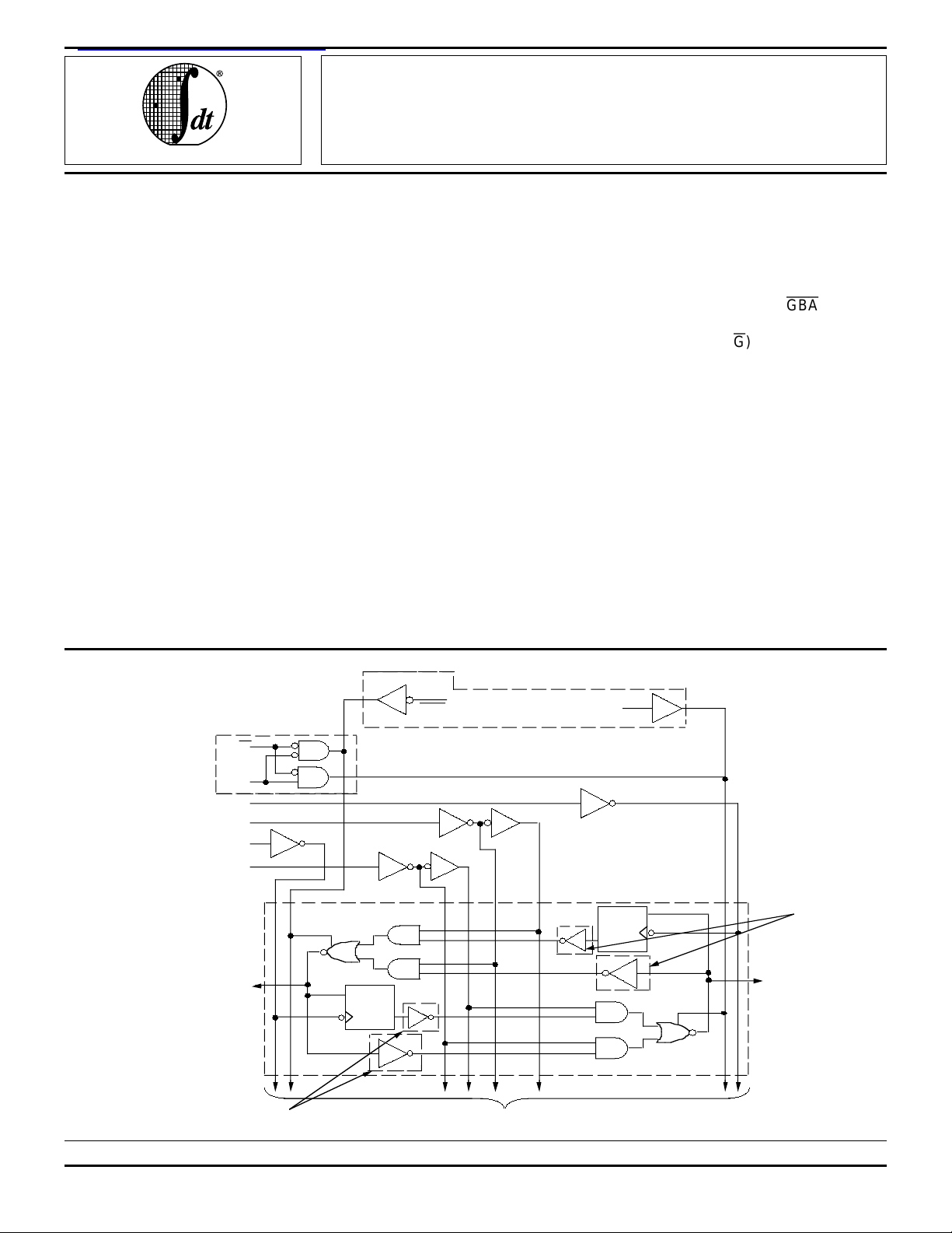
DESCRIPTION:
The FCT646T/FCT2646T/FCT648T/FCT652T/2652T consist of a bus transceiver with 3-state D-type flip-flops and
control circuitry arranged for multiplexed transmission of data
directly from the data bus or from the internal storage registers.
The FCT652T/FCT2652T utilize GAB and
control the transceiver functions. The FCT646T/FCT2646T/
FCT648T utilize the enable control (G) and direction (DIR)
pins to control the transceiver functions.
SAB and SBA control pins are provided to select either realtime or stored data transfer. The circuitry used for select
control will eliminate the typical decoding glitch that occurs in
a multiplexer during the transition between stored and realtime data. A LOW input level selects real-time data and a
HIGH selects stored data.
Data on the A or B data bus, or both, can be stored in the
internal D flip-flops by LOW-to-HIGH transitions at the appropriate clock pins (CPAB or CPBA), regardless of the select or
enable control pins.
The FCT26xxT have balanced drive outputs with current
limiting resistors. This offers low ground bounce, minimal
undershoot and controlled output fall times-reducing the need
for external series terminating resistors. FCT2xxxT parts are
plug-in replacements for FCTxxxT parts.
GBA
signals to
FUNCTIONAL BLOCK DIAGRAM
IDT54/74FCT646/2646/648
646/2646/652/2652
The IDT logo is a registered trademark of Integrated Device Technology, Inc.
DIR
CPBA
SBA
CPAB
SAB
ONLY
ONLY
G
A1
1 OF 8 CHANNELS
A REG
1D
C1
GBA
TO 7 OTHER CHANNELS
IDT54/74FCT652/2652
ONLY
GAB
B REG
C1
1D
646/2646/652/2652
ONLY
B1
2634 drw 01
MILITARY AND COMMERCIAL TEMPERATURE RANGES SEPTEMBER 1996
1996 Integrated Device Technology, Inc. 6.20 DSC-2634/9
1

IDT54/74FCT646/2646/652/2652T/AT/CT/DT, 648T/AT/CT
FAST CMOS OCTAL TRANSCEIVER/REGISTER MILITARY AND COMMERCIAL TEMPERATURE RANGES
PIN CONFIGURATIONS
CPAB
SAB
DIR
GND
CPAB
SAB
GAB
GND
2
3
P24-1
4
A
A2
A3
A4
A5
A6
A
A8
1
7
5
6
7
8
9
10
11
D24-1
SO24-2
SO24-7*
SO24-8
SO24-9*
&
E24-1
12
DIP/SOIC/SSOP/
QSOP/TSSOP/CERPACK
TOP VIEW
* FCT646/2646T/AT/CT/DT only
2
3
P24-1
4
A
A2
A3
A4
A5
A6
A
A8
1
7
5
6
7
8
9
10
11
D24-1
SO24-2
SO24-7*
SO24-8
&
E24-1
12
DIP/SOIC/SSOP/
QSOP/CERPACK
TOP VIEW
* FCT652/2652T/AT/CT/DT only
24
23
22
21
20
19
18
17
16
15
14
13
24
23
22
21
20
19
18
17
16
15
14
13
VCC1
CPBA
SBA
G
B
1
B2
B3
B4
B5
B6
B7
8
B
2634 drw 02
VCC1
CPBA
SBA
GBA
B
1
B2
B3
B4
B5
B6
B7
8
B
2634 drw 04
FCT646/FCT2646T
FCT648
FCT652/FCT2652T
INDEX
INDEX
NC
A1
A2
A3
NC
A
A5
A6
A1
A2
A3
A
A5
A6
CPAB
1
L28-1
15
GND
LCC
CPAB
1
L28-1
15
GND
LCC
NC
NC
NC
NC
CC
V
8
B
CC
V
8
B
CPBA
SBA
262728
25
24
23
22
21
20
19
181716
B7
B6
CPBA
SBA
262728
25
24
23
22
21
20
19
181716
B7
B6
G
1
B
B2
NC
3
B
B4
B5
2634 drw 03
GBA
B
1
B2
NC
B
3
B4
B5
2634 drw 05
SAB
DIR
32
4
5
6
7
8
4
9
10
11
5
6
7
8
4
9
10
11
1213
7
A
GAB
4
1213
7
A
32
14
A8
TOP VIEW
SAB
14
A8
TOP VIEW
PIN DESCRIPTION
Pin Names Description
A1 - A
8
B1 - B
8
CPAB, CPBA Clock Pulse Inputs
SAB, SBA Output Data Source Select Inputs
DIR,
G
GAB,
GBA
6.20 2
Data Register A Inputs
Data Register B Outputs
Data Register B Inputs
Data Register A Outputs
Output Enable Inputs (646/648)
Output Enable Inputs (652)
2634 tbl 01
IDT54/74FCT646/2646/652/2652T/AT/CT/DT, 648T/AT/CT
FAST CMOS OCTAL TRANSCEIVER/REGISTER MILITARY AND COMMERCIAL TEMPERATURE RANGES
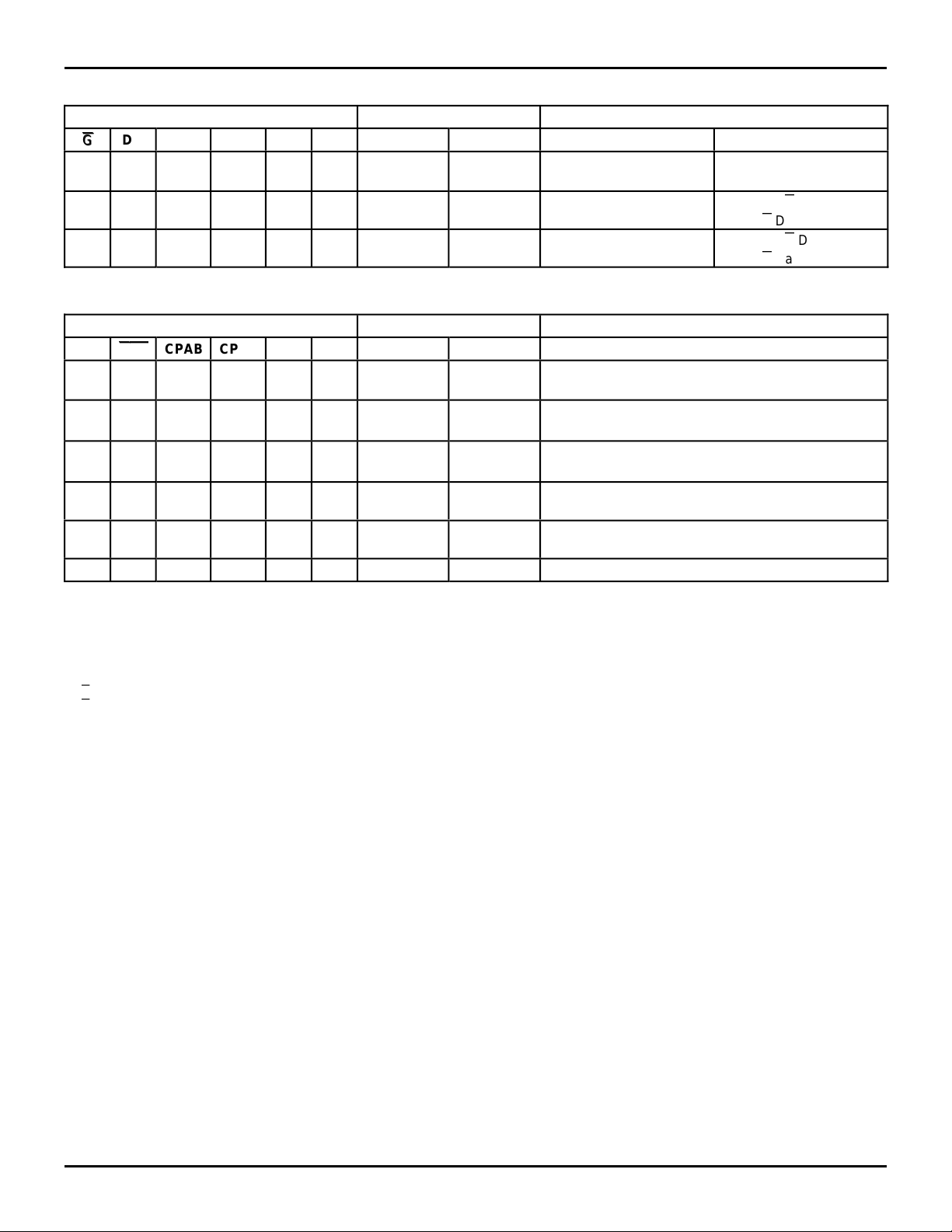
FUNCTION TABLE (646/648)
Inputs Data I/O
GGDIR CPAB CPBA SAB SBA A1 - A8 B1 - B8 FCT646T/FCT2646T FCT648T
H
XXH or L↑H or L↑X
H
L
L
L
L
L
L
H
HXH or L
X
X
X
H or LXX
X
X
X
X
X
L
Input Input Isolation
Output Input Real-Time B Data to A Bus
H
L
X
H
X
Input Output Real-Time A Data to B Bus
(1)
Operation or Function
Store A and B Data
Stored B Data to A Bus
Stored A Data to B Bus
Isolation
Store A and B Data
Real-Time B Data to A Bus
Stored B Data to A Bus
Real-Time A Data to B Bus
Stored A Data to B Bus
2634 tbl 02
FUNCTION TABLE (652)
Inputs Data I/O Operation or Function
GAB
NOTES: 2634 tbl 03
1. The data output functions may be enabled or disabled by various signals at the GAB or GBA inputs. Data
2. Select control = L: clocks can occur simultaneously.
3.A in B Register.
4.B in A Register.
GBA
CPAB CPBA SAB SBA A1 - A8 B1 - B8 FCT652T/FCT2652T
GBA
L
HHH or L↑H or L↑X
L
X
H
L
L
L
L
H
H
H
H
XLH or L
L
L
H
HXH or L
↑
↑
↑
X
X
H or L↑X
X
↑
↑
X
H or LXX
X
X
X
(2)
X
XXX
L
H
X
X
X
X
(2)
L
H
X
X
Input Input Isolation
Store A and B Data
Input
Input
(1)
Store A, Hold B
Store A in Both Registers
Hold A, Store B
Store B in Both Registers
Input
Input
Unspecified
Output
Unspecified
Output
(1)
Output Input Real-Time B Data to A Bus
Stored B Data to A Bus
Input Output Real-Time A Data to B Bus
Stored A Data to B Bus
H L H or L H or L H H Output Output Stored A Data to B Bus and Stored B Data to A Bus
input functions are always enabled, i.e. data at the bus pins will be stored on every LOW-to-HIGH transition
on the clock inputs.
Select control = H: clocks must be staggered in order to load both registers.
H = HIGH, L = LOW, X = Don't Care, ≠ = LOW-to-HIGH transition.
6.20 3
 Loading...