

Integrated Device Technology Inc IDT49C460AFF, IDT49C460AFFB, IDT49C460AG, IDT49C460CG, IDT49C460CGB Datasheet
...
Integrated Device Technology, Inc.
32-BIT CMOS
ERROR DETECTION
AND CORRECTION UNIT
IDT49C460
IDT49C460A
IDT49C460B
IDT49C460C
IDT49C460D
IDT49C460E
FEATURES:
• Fast
Detect Correct
— IDT49C460E 10ns (max.) 14ns (max.)
— IDT49C460D 12ns (max.) 18ns (max.)
— IDT49C460C 16ns (max.) 24ns (max.)
— IDT49C460B 25ns (max.) 30ns (max.)
— IDT49C460A 30ns (max.) 36ns (max.)
— IDT49C460 40ns (max.) 49ns (max.)
• Low-power CMOS
— Commercial: 95mA (max.)
— Military: 125mA (max.)
• Improves system memory reliability
— Corrects all single bit errors, detects all double and some
triple-bit errors
• Cascadable
— Data words up to 64-bits
• Built-in diagnostics
— Capable of verifying proper EDC operation via software
control
• Simplified byte operations
— Fast byte writes possible with separate byte enables
• Functional replacement for 32- and 64-bit configurations of
the AM29C60 and AM29C660
• Available in PGA, PLCC and Fine Pitch Flatpack
• Military product compliant to MIL-STD-883, Class B
• Standard Military Drawing #5962–88533
DESCRIPTION:
The IDT49C460s are high-speed, low-power, 32-bit Error
Detection and Correction Units which generate check bits on
a 32-bit data field according to a modified Hamming Code and
correct the data word when check bits are supplied. The
IDT49C460s are performance-enhanced functional replacements for 32-bit versions of the 2960. When performing a read
operation from memory, the IDT49C460s will correct 100% of
all single bit errors and will detect all double bit errors and
some triple bit errors.
The IDT49C460s are easily cascadable to 64-bits. Thirtytwo-bit systems use 7 check bits and 64-bit systems use 8
check bits. For both configurations, the error syndrome is
made available.
The IDT49C460s incorporate two built-in diagnostic modes.
Both simplify testing by allowing for diagnostic data to be
entered into the device and to execute system diagnostics
functions.
They are fabricated using a CMOS technology designed for
high-performance and high-reliability. The devices are packaged in a 68-pin ceramic PGA, PLCC and Ceramic Quad
Flatpack.
Military grade product is manufactured in compliance with
the latest revision of MIL-STD-883, Class B, making it ideally
suited to military temperature applications demanding the
highest level of performance and reliability.
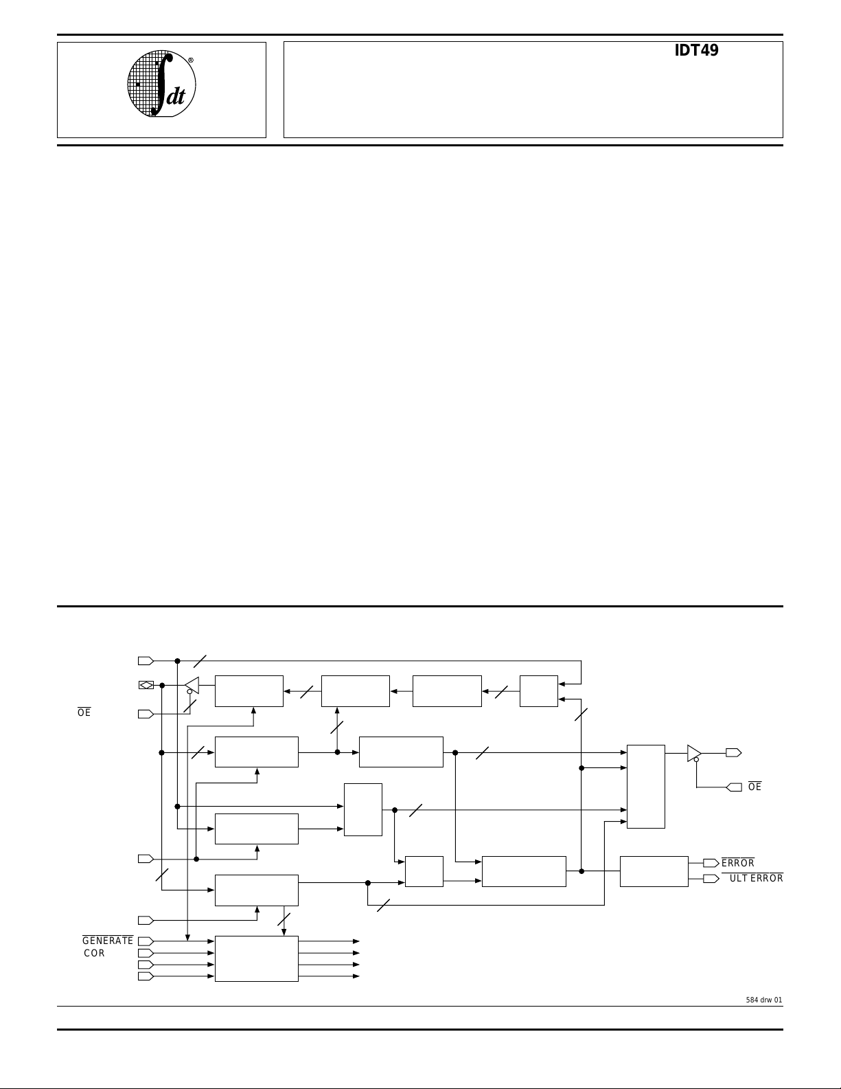
FUNCTIONAL BLOCK DIAGRAM
CB
0–7
DATA0–31
OE
BYTE0–3
LEIN
LEDIAG
LEOUT/
GENERATE
CORRECT
1,0
CODE ID
DIAG MODE1,0
The IDT logo is a registered trademark of Integrated Device Technology, Inc.
MILITARY AND COMMERCIAL TEMPERATURE RANGES AUGUST 1995
1995 Integrated Device Technology, Inc. 11.6 DSC-9017/8
8
DATA
LATCH
4
DATA
LATCH
32
CHECK BIT
IN LATCH
13
DIAGNOSTIC
LATCH
CONTROL
LOGIC
5
32
ERROR
CORRECT
32
MUX
CHECK BIT
GENERATE
MUX
8
ERROR
DECODE
8
8
8
SYNDROME
GENERATE
MUX
8
SC0–7
MUX
ERROR
DETECT
OE
SC
ERROR
MULT ERROR
2584 drw 01
1
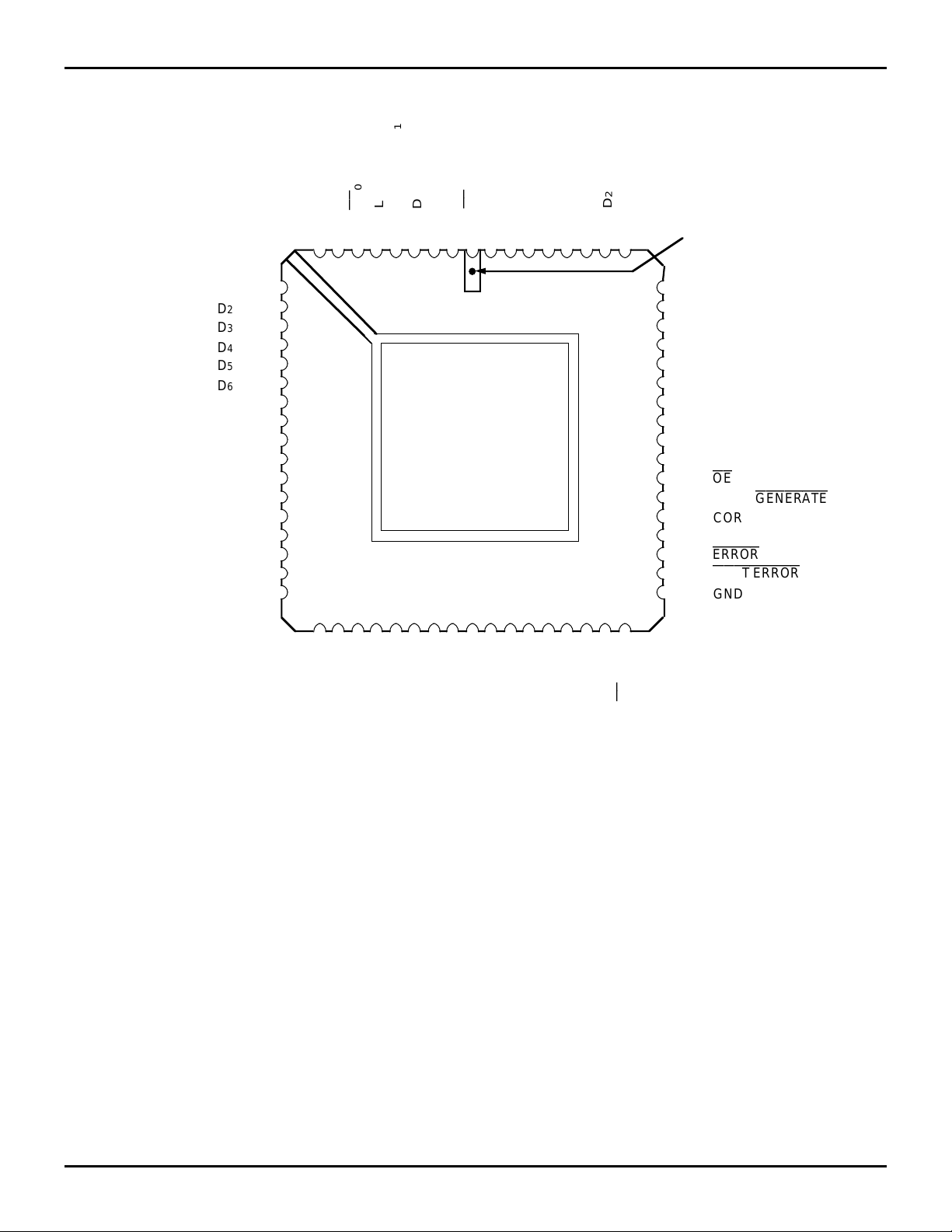
IDT49C460/A/B/C/D/E
32-BIT CMOS ERROR DETECTION AND CORRECTION UNIT MILITARY AND COMMERCIAL TEMPERATURE RANGES
PIN CONFIGURATIONS
V
CC
D
D
D
D
D
D
D
GND
D
D
10
D
11
D
12
D
13
D
14
D
15
OE1
0
D1
D0
OE
DIAG MODE1
LEIN
DIAG MODE0
OE3D31
CODE ID1
CODE ID0
29
D30
D28
D27
D26
D25
D
GND
DESIGNATES
9876543216867666564636261
PIN 1 FOR
PLCC ONLY
10
11
2
12
3
13
4
14
5
15
6
16
7
17
8
18
19
9
J68–1
20
21
22
23
24
25
26
60
D
59
D
58
D
57
D
56
D
55
D
54
D
53
D
52
V
51
D
OE
50
49
LE
48
CORRECT
47
LE
ERROR
46
MULT ERROR
45
44
GND
24
23
22
21
20
19
18
17
CC
16
2
OUT
DIAG
/
GENERATE
27 28 29 30 31 32 33 34 35 36 37 38 39 40 41 42 43
CB6
CB5
CB4
CB3
CB2
CB1
CB0
SC1
SC2
SC3
SC4
SC5
SC6
CB7
SC0
SC7
PLCC
TOPVIEW
SC
2584 drw 02
OE
11.6 2
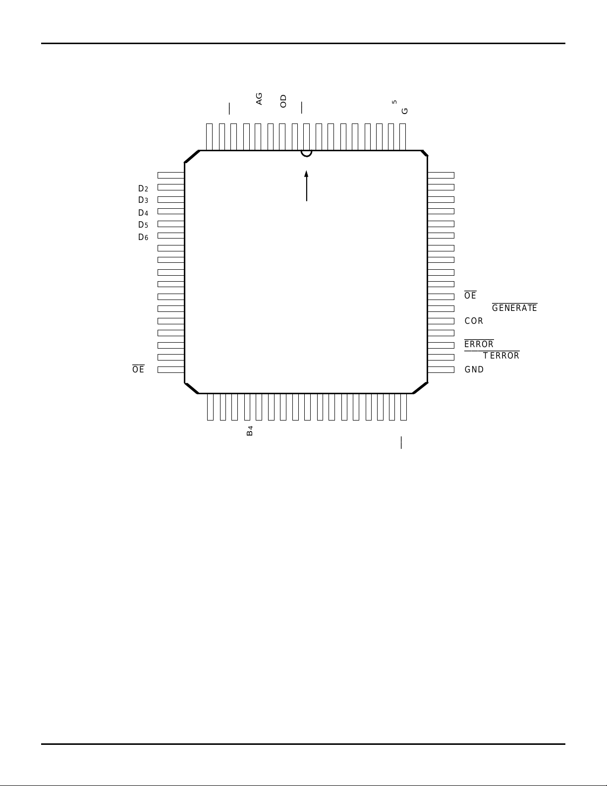
IDT49C460/A/B/C/D/E
32-BIT CMOS ERROR DETECTION AND CORRECTION UNIT MILITARY AND COMMERCIAL TEMPERATURE RANGES
1
0
0
1
VCC
D
D
D4
D5
D6
D7
D8
GND
D9
D10
D11
D12
D13
D14
D15
OE
1D0
D
IN
OE0LE
DIAG MODE
DIAG MODE
3
OE
CODE ID
CODE ID
29
D31D30D28D27D26D25GND
D
98765432168 67 66 65 64 63 62 61
10
2
3
11
12
13
PIN 1 IDENTIFICATION
14
15
16
17
18
F68 - 2
19
20
21
22
23
24
25
1
26
60
59
58
57
56
55
54
53
52
51
50
49
48
47
46
45
44
D24
D23
D22
D21
D20
D19
D18
D17
VCC
D16
OE
2
LEOUT/
GENERATE
CORRECT
DIAG
LE
ERROR
MULT ERROR
GND
27 28 29 30 31 32 33 34 35 36 37 38 39 40 41 42 43
7
CB6CB5CB4CB3CB2CB1CB0SC1SC2SC3SC4SC
CB
0
SC
FINE PITCH FLATPACK
TOPVIEW
2584 drw 03
5
7
6
SC
SC
SC
OE
11.6 3
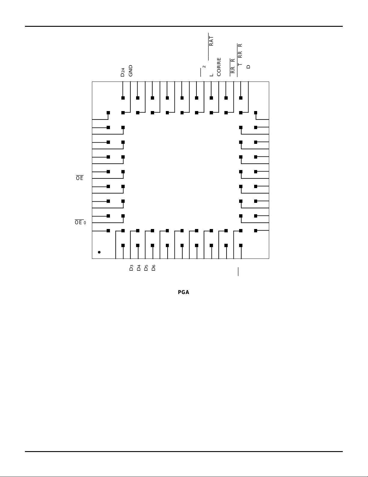
IDT49C460/A/B/C/D/E
E
32-BIT CMOS ERROR DETECTION AND CORRECTION UNIT MILITARY AND COMMERCIAL TEMPERATURE RANGES
GENERAT
D
D27
D26
D29
D28
D31
D30
CODE ID0
OE
DIAG MODE0
CODE ID1
LEIN
DIAG MODE1
D0
OE
D1
24
GND
D23
D22
D21
D20
D
D19
VCC
D18
D17
OE 2LEOUT/
D16
5152504948474645444342414039383736
25
DIAG
CORRECT
ERROR
LE
35
32 3355 54
GND
MULT ERROR
3453
OESC
SC7
SC6
30 3157 56
SC5
SC4
28 2959 58
SC3
SC2
3
G68 – 1
26 2761 60
24 2563 62
SC1
SC0
CB0
CB1
22 2365 64
CB2
CB3
0
3456789101112131415
1
20 2167 66
68 19
2
161817
CB4
CB5
CB6
VCC
2584 drw 04
D3
D4
D5
D6
D2
D7
9
D8
D
D10
D12
GND
D11
D14
D13
1
D15
CB7
OE
PGA
TOPVIEW
11.6 4
IDT49C460/A/B/C/D/E
32-BIT CMOS ERROR DETECTION AND CORRECTION UNIT MILITARY AND COMMERCIAL TEMPERATURE RANGES
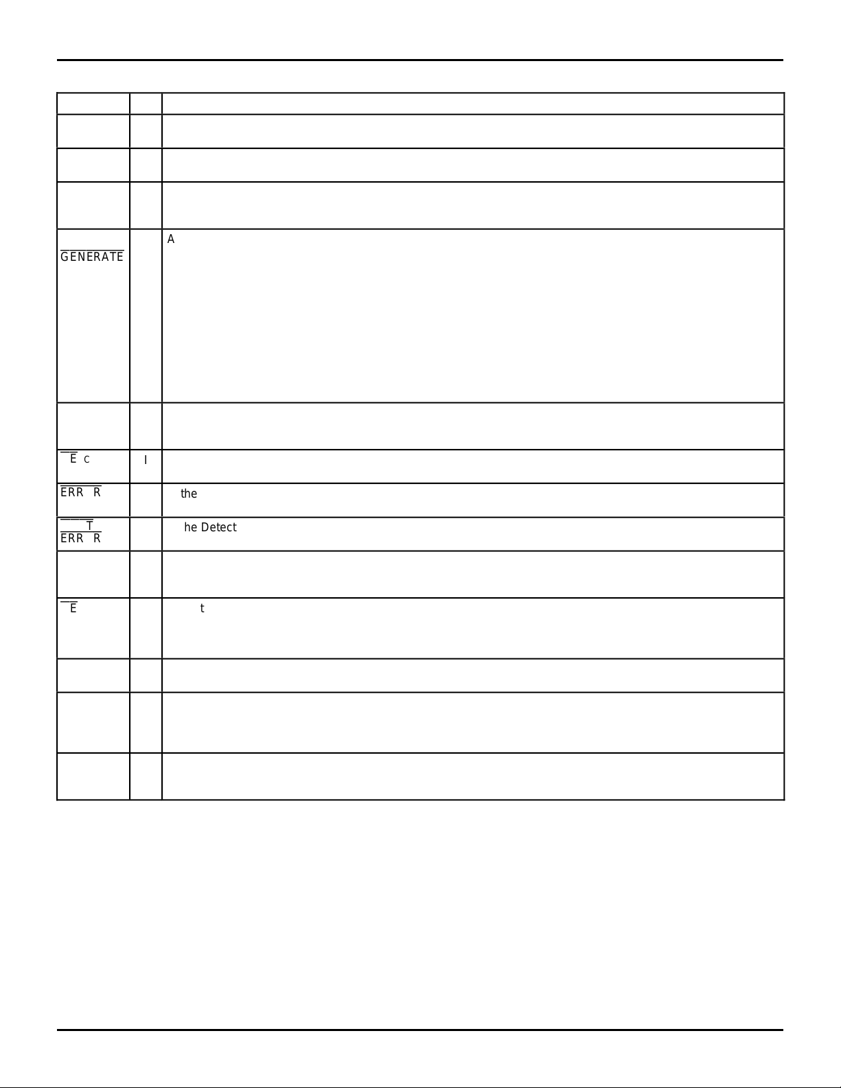
PIN DESCRIPTIONS
Pin Name I/O Description
DATA0–31 I/O 32 bidirectional data lines provide input to the Data Input Latch and Diagnostic Latch and also receive output from
the Data Output Latch. DATA
CB0–7 I Eight check bit input lines input check bits for error detection and also used to input syndrome bits for error
correction in 64-bit applications.
LEIN I Latch Enable is for the Data Input Latch. Controls latching of the input data. Data Input Latch and Check Bit Input
Latch are latched to their previous state when LOW. When HIGH, the Data Input Latch and Check Bit Input Latch
follow the input data and input check bits.
LEOUT/
GENERATE
A multifunction pin which, when LOW, is in the Check Bit Generate Mode. In this mode, the device generates the
check bits or GENERATE partial check bits specific to the data in the Data Input Latch. The generated check bits
are placed on the SC outputs. Also, when LOW, the Data Out Latch is latched to its previous state.
When HIGH, the device is in the Detect or Correct Mode. In this mode, the device detects single and multiple
errors and generates syndrome bits based upon the contents of the Data Input Latch and Check Bit Input Latch.
In the Correct Mode, single bit errors are also automatically corrected and the corrected data is placed at the
inputs of the Data Output Latch. The syndrome result is placed on the SC outputs and indicates in a coded form
the number of errors and the specific bit-in-error. When HIGH, the Data Output Latch follows the output of the
Data Input Latch as modified by the correction logic network. In Correct Mode, single bit errors are corrected by
the network before being loaded into the Data Output Latch. In Detect Mode, the contents of the Data Input Latch
are passed through the correction network unchanged into the Data Output Latch. The Data Output Latch is
disabled, with its contents unchanged, if the EDC is in the Generate Mode.
SC0–7 O Syndrome Check Bit outputs. Eight outputs which hold the check bits and partial check bits when the EDC is in
the Generate Mode and will hold the syndrome/partial syndrome bits when the device is in the Detect or Correct
modes. All are 3-state outputs.
OE
SC
I Output Enable—Syndrome Check Bits. In the HIGH condition, the SC outputs are in the high impedance state.
When LOW, all SC output lines are enabled.
ERROR
O In the Detect or Correct Mode, this output will go LOW if one or more data or check bits contain an error. When
HIGH, no errors have been detected. This pin is forced HIGH in the Generate Mode.
MULT
ERROR
O In the Detect or Correct Mode, this output will go LOW if two or more bit errors have been detected. A HIGH level
indicates that either one or no errors have been detected. This pin is forced HIGH in the Generate Mode.
CORRECT I The correct input which, when HIGH, allows the correction network to correct any single-bit error in the Data Input
Latch (by complementing the bit-in-error) before putting it into the Data Output Latch. When LOW, the device will
drive data directly from the Data Input Latch to the Data Output Latch without correction.
OE
BYTE0–3 I Output Enable—Bytes 0, 1, 2, 3. Data Output Latch. Control the three-state output buffers for each of the four
bytes of the Data Output Latch. When LOW, they enable the output buffer of the Data Output Latch. When HIGH,
they force the Data Output Latch buffer into the high impedance mode. One byte of the Data Output Latch is
easily activated by separately selecting the four enable lines.
DIAG
MODE
1,0
I Select the proper diagnostic mode. They control the initialization, diagnostic and normal operation of the EDC.
CODE ID1,0 I These two code identification inputs identify the size of the total data word to be processed. The two allowable
data word sizes are 32 and 64 bits and their respective modified Hamming Codes are designated 32/39 and
64/72. Special CODE ID
and CORRECT are to be taken from the Diagnostic Latch rather than from the input control lines.
LEDIAG I This is the Latch Enable for the Diagnostic Latch. When HIGH, the Diagnostic Latch follows the 32-bit data on the
input lines. When LOW, the outputs of the Diagnostic Latch are latched to their previous states. The Diagnostic
Latch holds diagnostic check bits and internal control signals for CODE ID
0 is the LSB; DATA31 is the MSB.
1,0, input 01 is also used to instruct the EDC that the signals CODE ID1,0, DIAG MODE1,0
1,0, DIAG MODE1,0 and CORRECT.
2584 tbl 01
11.6 5
IDT49C460/A/B/C/D/E
32-BIT CMOS ERROR DETECTION AND CORRECTION UNIT MILITARY AND COMMERCIAL TEMPERATURE RANGES
EDC ARCHITECTURE SUMMARY
The IDT49C460s are high-performance cascadable EDCs
used for check bit generation, error detection, error correction
and diagnostics. The function blocks for this 32-bit device
consist of the following:
• Data Input Latch
• Check Bit Input Latch
• Check Bit Generation Logic
• Syndrome Generation Logic
• Error Detection Logic
• Error Correction Logic
• Data Output Latch
• Diagnostic Latch
• Control Logic
DATA INPUT/OUTPUT LATCH
The Latch Enable Input, LEIN, controls the loading of 32 bits
of data to the Data In Latch. The data from the DATA lines can
be loaded in the Diagnostic Latch under control of the
Diagnostic Latch Enable, LEDIAG, giving check bit information
in one byte and control information in another byte. The
Diagnostic Latch is used in the Internal Control Mode or in one
of the diagnostic modes. The Data Output Latch has buffers
that place data on the DATA lines. These buffers are split into
four 8-bit buffers, each having their own output enable controls. This feature facilitates byte read and byte modify
operations.
CHECK BIT GENERATION LOGIC
This generates the appropriate check bits for the 32 bits of
data in the Data Input Latch. The modified Hamming Code is
the basis for generating the proper check bits.
SYNDROME GENERATION LOGIC
In both the Detect and Correct modes, this logic does a
comparison on the check bits read from memory against the
newly generated set of check bits produced for the data read
in from memory. Matching sets of check bits mean no error
was detected. If there is a mismatch, one or more of the data
or check bits is in error. Syndrome bits are produced by an
exclusive-OR of the two sets of check bits. Identical sets of
check bits mean the syndrome bits will be all zeros. If an error
results, the syndrome bits can be decoded to determine the
number of errors and the specific bit-in-error.
ERROR DETECTION LOGIC
This part of the device decodes the syndrome bits
generated by the Syndrome Generation Logic. With no errors
in either the input data or check bits, both the
MULTERROR
error is detected.
if two or more errors are detected.
outputs are HIGH. ERROR will go low if one
MULTERROR
and
ERROR
ERROR
will both go low
and
ERROR CORRECTION LOGIC
In single error cases, this logic complements (corrects) the
single data bit-in-error. This corrected data is loaded into the
Data Output Latch, which can then be read onto the bidirectional data lines. If the error is resulting from one of the check
bits, the correction logic does not place corrected check bits
on the syndrome/check bit outputs. If the corrected check bits
are needed, the EDC must be switched to the Generate Mode.
DATA OUTPUT LATCH AND OUTPUT BUFFERS
The Data Output Latch is used for storing the result of an
error correction operation. The latch is loaded from the
correction logic under control of the Data Output Latch Enable, LEOUT. The Data Output Latch may also be directly
loaded from the Data Input Latch in the PASSTHRU mode.
The Data Output Latch buffer is split into 4 individual buffers
which can be enabled by
the bidirectional data lines.
OE
0–3 separately for reading onto
DIAGNOSTIC LATCH
The diagnostic latch is loadable under control of the
Diagnostic Latch Enable, LEDIAG, from the bidirectional data
lines. Check bit information is contained in one byte while the
other byte contains the control information. The Diagnostic
Latch is used for driving the device when in the Internal Control
Mode, or for supplying check bits when in one of the diagnostic
modes.
CONTROL LOGIC
Specifies in which mode the device will be operating in.
Normal operation is when the control logic is driven by external
control inputs. In the Internal Control Mode, the control signals
are read from the Diagnostic Latch. Since LEOUT and
GENERATE
(LEOUT from high to low) of the Data Output Latch causes the
EDC to go into the Generate Mode.
are controlled by the same pin, the latching action
11.6 6
IDT49C460/A/B/C/D/E
32-BIT CMOS ERROR DETECTION AND CORRECTION UNIT MILITARY AND COMMERCIAL TEMPERATURE RANGES
DETAILED PRODUCT DESCRIPTION
The IDT49C460 EDC units contain the logic necessary to
generate check bits on 32 bits of data input according to a
modified Hamming Code. The EDC can compare internally
generated check bits against those read with the 32-bit data
to allow correction of any single bit data error and detection of
all double (and some triple) bit errors. The IDT49C460s can
be used for 32-bit data words (7 check bits) and 64-bit (8 check
bits) data words.
WORD SIZE SELECTION
The two code identification pins, CODE ID1, 0, are used to
determine the data word size that is 32 or 64 bits. They also
select the Internal Control Mode. Table 4 defines all possible
slice identification codes.
CHECK AND SYNDROME BITS
The IDT49C460s provide either check bits or syndrome
bits on the three-state output pins, SC0–7. Check bits are
generated from a combination of the Data Input bits, while
syndrome bits are an exclusive-OR of the check bits generated from read data with the read check bits stored with the
data. Syndrome bits can be decoded to determine the single
bit in error or that a double (some triple) error was detected.
The check bits are labeled:
Correct
Diag
Mode
0
Diag
Mode
Diagnostic Mode Selected
1
X00Non-diagnostic Mode. Normal
EDC function in this mode.
X01Diagnostic Generate. The con
tents of the Diagnostic Latch are
substituted for the normally
generated check bits when in the
Generate Mode. The EDC
functions normally in the Detect or
Correct modes.
0/1 1 0 Diagnostic Detect/Correct. In
either mode, the contents of the
Diagnostic Latch are substituted
for the check bits normally read
from the Check Bit Input Latch.
The EDC functions normally in the
Generate Mode.
111Initialize. The Data Input Latch
outputs are forced to zeros and
latched upon removal of Initialize
Mode.
011PASSTHRU.
2584 tbl 02
Table 2. Diagnostic Mode Control
C
0, C1, C2, C3, C4, C5, C6 for the 32-bit configuration
C0, C1, C2, C3, C4, C5, C6, C7 for the 64-bit configuration
Syndrome bits are similarly labeled S
Operating
Mode
Generate 0
Detect 0
Correct 0
PASSTHRU 1 1 1 0 DATAIN Latch Check Bit Latch High
Diagnostic
Generate
Diagnostic Detect 1 0 1 0 DATAIN Latch Syndrome Bits DATAIN/
Diagnostic Correct 1 0 1 1 DATAIN Latch w/
Initialization 1 1 1 1 DATAIN Latch
Internal CODE ID1,0 = 01 (Control Signals CODE ID1,0, DIAG MODE1,0 and CORRECT are taken from Diagnostic Latch.)
NOTES:
1. In Generate Mode, data is read into the EDC unit and the check bits are generated. The same data is written to memory along with the check bits. Since
the DATA
2. Error Dep (Error Dependent):
for no errors.
3. LE
OUT Latch is not used in the Generate Mode, LEOUT (being LOW since it is tied to Generate) does not affect the writing of check bits.
IN is LOW.
DM
0 DM1 Generate Correct DATAOUT Latch
0
1
0
0
0
1
0
0
1
0 1 0 X — Check Bits from Diagnostic Latch High
ERROR
0 through S7.
SC
(
OE
SC = LOW)
OE
0XLEOUT = LOW
(1)
Check Bits Generated from
DATA
1 0 DATAIN Latch Syndrome Bits DATAIN/
Check Bit Latch
1 1 DATAIN Latch w/
Single Bit Correction
Syndrome Bits DATAIN/
Check Bit Latch
Diagnostic Latch
Syndrome Bits DATAIN/
Single Bit Correction
Set to 0000
will be low for single or multiple errors, with
Table 3. IDT49C460 Operating Modes
(3)
MULT ERROR
Diagnostic Latch
low for double or multiple errors. Both signals are high
ERROR
0–7
ERROR
MULT ERROR
MULT ERROR
High
IN Latch
Error Dep
(2)
Error Dep
Error Dep
Error Dep
——
2584 tbl 03
11.6 7
IDT49C460/A/B/C/D/E
OE
32-BIT CMOS ERROR DETECTION AND CORRECTION UNIT MILITARY AND COMMERCIAL TEMPERATURE RANGES
OPERATING MODE SELECTION
Tables 2 and 3 describe the nine operating modes of the
IDT49C460s. The Diagnostic Mode pins — DIAG MODE0,1
— define four basic areas of operation.
CORRECT further divide operation into 8 functions, with
CODE ID1,0 defining the ninth mode as the Internal Mode.
Generate Mode is used to display the check bits on the
outputs SC0–7. The Diagnostic Generate Mode displays
check bits as stored in the Diagnostic Latch.
Detect Mode provides an indication of errors or multiple
errors on the outputs
ERROR
and
MULT ERROR
errors are not corrected in this mode. The syndrome bits are
provided on the outputs SC0–7. For the Diagnostic Detect
Mode, the syndrome bits are generated by comparing the
internally generated check bits from the Data In Latch with
Code ID1 Code ID0 Slice Selected
0 0 32-Bit
0 1 Internal Control Mode
1 0 64-Bit, Lower 32–Bit (0–31)
1 1 64-Bit, Upper 32-Bit (32–63)
Table 4. Slice Identification
DATA0–31
HIGH
C6
GENERATE
. Single bit
C0
and
2584 tbl 04
check bits stored in the diagnostic latch rather than with the
check bit latch contents.
Correct Mode is similar to the Detect Mode except that
single bit errors will be complemented (corrected) and made
available as input to the Data Out Latches. Again, the
Diagnostic Correct Mode will correct single bit errors as
determined by syndrome bits generated from the data input
and contents of the diagnostic latches.
The Initialize Mode provides check bits for all zero bit data.
Data Input Latches are set, latched to a logic zero and made
available as input to the Data Out Latches.
The Internal Mode disables the external control pins DIAG
MODE
0,1 and CORRECT to be defined by the Diagnostic
Latch. Even CODE ID1,0, although externally set to the 01
code, can be redefined from the Diagnostic Latch data.
SC
DATA INPUT
DATA0–31DATA32–63
DATA CB0–7
(LOWER 32 BITS)
32
CHECK–BIT INPUTS
32
IDT49C460
SC0–7
8
CODE ID1,0
OE
1/8
IDT74FCT240
SC
1,0
DATA0–31
SC
SC7
NC
S6/C6
6
CB
CB7
SC5
S5/C5
6
CB5C5CB4C4CB3C3CB2C2CB1C1CB0
IDT49C460
SC4
SC3
S3/C3
S4/C4
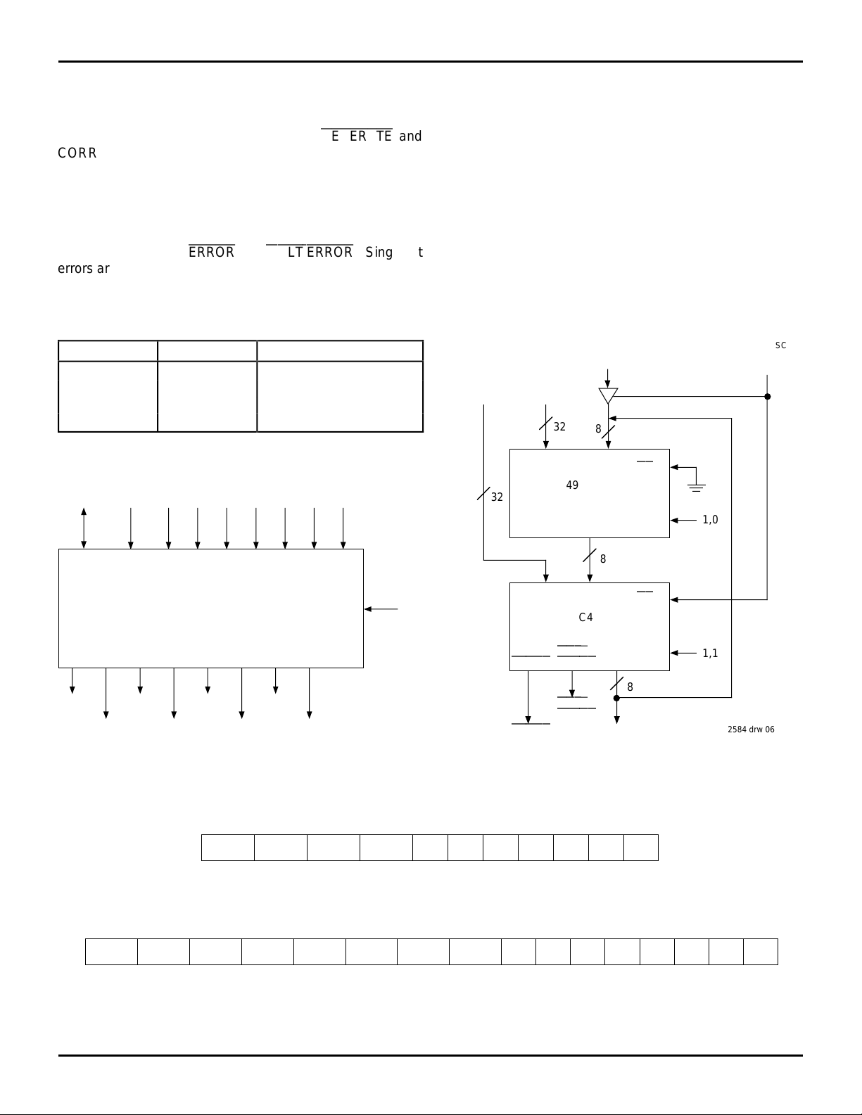
Figure 1. 32-Bit Configuration
S2/C2
SC2
SC1
S1/C1
CODE ID1,0
SC0
S0/C0
2584 drw 05
0,0
8
DATA CB
IDT49C460
(UPPER 32 BITS)
ERROR
ERROR
Figure 2. 64-Bit Configuration
MULT
ERROR
MULT
ERROR
0–7
CODE ID1,0
SC0–7
8
SYNDROME/
CHECK BITS
OE
SC
DATA CHECK BITS
BYTE3 BYTE2 BYTE1 BYTE0 C0 C1 C2 C3 C4 C5 C6
0781516232431
Figure 3. 32-Bit Data Format
2584 drw 07
DATA CHECK BITS
BYTE7 BYTE6 BYTE5 BYTE4 BYTE3 BYTE2 BYTE1 BYTE0 C0 C1 C2 C3 C4 C5 C6 C7
07815162324313239404748555663
Figure 4. 64-Bit Data Format
1,1
2584 drw 06
2584 drw 08
11.6 8
IDT49C460/A/B/C/D/E
32-BIT CMOS ERROR DETECTION AND CORRECTION UNIT MILITARY AND COMMERCIAL TEMPERATURE RANGES
32-BIT DATA WORD CONFIGURATION
A single IDT49C460 EDC unit, connected as shown in
Figure 1, provides all the logic needed for single bit error
correction and double bit error detection of a 32-bit data field.
The identification code indicates 7 check bits are required.
The CB7 pin should be HIGH.
Figure 3 indicates the 39-bit data format for two bytes of
data and 7 check bits. Table 3 describes the operating mode
available.
Table 6 indicates the data bits participating in the check bit
generation. For example, check bit C0 is the exclusive-OR
function of the 16 data input bits marked with an X. Check bits
are generated and output in the Generate and Initialization
Mode. Check bits from the respective latch are passed,
unchanged, in the PASSTHRU or Diagnostic Generate Mode.
Syndrome bits are generated by an exclusive-OR or the
BIT 0 CB0 DIAGNOSTIC
BIT 1 CB1 DIAGNOSTIC
BIT 2 CB2 DIAGNOSTIC
BIT 3 CB3 DIAGNOSTIC
BIT 4 CB4 DIAGNOSTIC
BIT 5 CB5 DIAGNOSTIC
BIT 6 CB6 DIAGNOSTIC
BIT 7 CB7 DIAGNOSTIC
BIT 8 CODE ID
BIT 9 CODE ID
BIT 10 DIAG MODE
BIT 11 DIAG MODE
BIT 12 CORRECT
BIT 13–31 DON'T CARE
Table 5. 32-Bit Diagnostic Latch Coding Format
generated check bits with the read check bits. For example,
S
n is the XOR of check bits Cn from those read with those
generated. Table 7 indicates the decoding of the seven
syndrome bits to identify the bit-in-error for a single bit error,
or whether a double or triple bit error was detected. The all
zero case indicates no errors detected.
In the Correct Mode, the syndrome bits are used to
complement (correct) single bit errors in the data bits. For
double or multiple error detection, the data available as input
to the Data Out Latch is not defined.
Table 5 defines the bit definition for the Diagnostic Latch.
As defined in Table 3, several modes will use the diagnostic
check bits to determine syndrome bits or to pass as check bits
to the SC0–7 outputs. The Internal Mode substitutes the
indicated bit position for the external control signals.
0
1
0
1
2584 drw 05
Generated
Check Bits Parity 0123456789101112131415
C0 Even (XOR) X X X X X X X X
C1 Even (XOR) X X X X X X X X
C2 Odd (XNOR) X X X X X X X X
C3 Odd (XNOR) X X X X X X X X
C4 Even (XOR) X X X X X X X X
C5 Even (XOR) X X X X X X X X
C6 Even (XOR) XXXXXXXX
Generated
Check Bits Parity 16 17 18 19 20 21 22 23 24 25 26 27 28 29 30 31
C0 Even (XOR) X X X X X X X X
C1 Even (XOR) X X X X X X X X
C2 Odd (XNOR) X X X X X X X X
C3 Odd (XNOR) X X X X X X X X
C4 Even (XOR) X X X X X X X X
C5 Even (XOR) X X X X X X X X
C6 Even (XOR) X X X X X X X X
Table 6. 32–Bit Modified Hamming Code–Check Bit Encode Chart
Participating Data Bits
2584 tbl 06
Participating Data Bits
2584 tbl 07
11.6 9
IDT49C460/A/B/C/D/E
32-BIT CMOS ERROR DETECTION AND CORRECTION UNIT MILITARY AND COMMERCIAL TEMPERATURE RANGES
Hex 01234567
Syndrome
Bits
Hex S3 S2 S1 S0
0 0 0 0 0 * C4 C5 T C6 T T 30
1 0 0 0 1 C0 T T 14 T M M T
20010 C1TTMT224T
30011 T188TMTTM
4 0 1 0 0 C2 T T 15 T 3 25 T
50101 T199TMTT31
60110 T2010TMTTM
70111 MTTMT426T
81000 C3TTMT527T
91001 T2111TMTTM
A1010 T2212T1TTM
B1011 17TTMT628T
C1100 T2313TMTTM
D1101 MTTMT729T
E1110 16TTMTMMT
F1111 TMMT0TTM
NOTES: 2584 tbl 08
1. * = No errors detected
2. Number = The number of the single bit-in-error
3. T = Two errors detected
4. M = Three or more errors detected
Table 7. Syndrome Decode to Bit-in-Error (32-Bit)
00001111
S
6
00110011
S
5
01010101
S4
64-BIT DATA WORD CONFIGURATION
Two IDT49C460 EDC units, connected as shown in Figure
2, provide all the logic needed for single bit error detection and
double bit error detection of a 64-bit data field. Table 4 gives
the CODE ID1,0 values needed for distinguishing the upper 32
bits from the lower 32 bits. Valid syndrome, check bits and the
ERROR
CODE ID1,0 = 11. Control signals not indicated are connected
to both units in parallel. The EDC with the CODE ID1,0 = 10
has the
from the EDC with CODE ID1,0 = 11 and also controls the
check bit buffers from memory.
numbered inputs of the EDC unit with CODE ID1,0 = 10, while
Data In bits 32 through 63 are connected to Data Inputs 0 to
31, respectively, for the EDC unit with CODE ID1,0 = 11.
and 8 check bits. Check bits are input to the EDC unit with
CODE ID1,0 = 10 through a three-state buffer unit such as the
IDT74FCT244. Correction of single bit errors of the 64-bit
configuration requires a feedback of syndrome bits from the
upper EDC unit to the lower EDC unit. The MUX shown on the
functional block diagram is used to select the CB
the syndrome bits rather than internally generated syndrome
bits.
and
MULT ERROR
OE
SC grounded. The OESC selects the syndrome bits
signals come from the IC with the
Data In bits 0 through 31 are connected to the same
Figure 4 indicates the 72-bit data format of 8 bytes of data
0–7 pins as
Table 3 describes the operating modes available for the 64/
72 configuration.
Table 11 indicates the data bits participating in the check bit
generation. For example, check bit C0 is the exclusive-OR
function of the 32 data input bits marked with an X. Check bits
are generated and output in the Generate and Initialization
modes. Check bits are passed as stored in the PASSTHRU or
Diagnostic Generate modes.
Syndrome bits are generated by an exclusive-OR of the
generated check bits with the read check bits. For example,
Sn is the XOR of check bits Cn from those read with those
generated. Table 9 indicates the decoding of the 8 syndrome
bits to determine the bit in error for a single bit error or whether
a double or triple bit error was detected. The all zero case
indicates no errors detected.
In the Correct Mode, the syndrome bits are used to
complement (correct) single bit errors in the data bits. For
double or multiple error detection, the data available as input
to the Data Out Latch is not defined.
Tables 8A and 8B define the bit definition for the Diagnostic
Latch. As defined in Table 3, several modes will use the
Diagnostic Check Bits to determine syndrome bits or to pass
as check bits to the SC
0–7 outputs. The Internal Mode sub-
stitutes the indicated bit position for the external control
signals.
Performance data is provided in Table 10, relating a single
IDT49C460 EDC with the two cascaded units of Figure 2. As
indicated, a summation of propagation delays is required from
the cascading arrangement of EDC units.
Bit Internal Function
0CB
1CB
2CB
3CB
4CB
5CB
6CB
7CB
8 CODE ID0 LOWER 32-BIT
9 CODE ID1 LOWER 32-BIT
10 DIAG MODE0 LOWER 32-BIT
11 DIAG MODE1 LOWER 32-BIT
12 CORRECT LOWER 32-BIT
13–31 DON'T CARE
32–39 DON'T CARE
40 CODE ID0 UPPER 32-BIT
41 CODE ID1 UPPER 32-BIT
42 DIAG MODE0 UPPER 32-BIT
43 DIAG MODE1 UPPER 32-BIT
44 CORRECT UPPER 32-BIT
45–63 DON'T CARE
Table 8A. 64-Bit Diagnostic Latch–Coding Format
(Diagnostic and Correct Mode)
0
DIAGNOSTIC
1
DIAGNOSTIC
2
DIAGNOSTIC
3
DIAGNOSTIC
4
DIAGNOSTIC
5
DIAGNOSTIC
6
DIAGNOSTIC
7
DIAGNOSTIC
2584 tbl 09
11.6 10

IDT49C460/A/B/C/D/E
32-BIT CMOS ERROR DETECTION AND CORRECTION UNIT MILITARY AND COMMERCIAL TEMPERATURE RANGES
Bit Internal Function
0–7 DON'T CARE
8 CODE ID0 LOWER 32-BIT
9 CODE ID1 LOWER 32-BIT
10 DIAG MODE0 LOWER 32-BIT
11 DIAG MODE1 LOWER 32-BIT
12 CORRECT LOWER 32-BIT
13–31 DON'T CARE
32 CB0 DIAGNOSTIC
33 CB1 DIAGNOSTIC
34 CB2 DIAGNOSTIC
35 CB3 DIAGNOSTIC
36 CB4 DIAGNOSTIC
37 CB5 DIAGNOSTIC
38 CB6 DIAGNOSTIC
39 CB7 DIAGNOSTIC
40 CODE ID0 UPPER 32-BIT
41 CODE ID1 UPPER 32-BIT
42 DIAG MODE0 UPPER 32-BIT
43 DIAG MODE1 UPPER 32-BIT
44 CORRECT UPPER 32-BIT
45–63 DON'T CARE
2584 tbl 10
Table 8B. 64-Bit Diagnostic Latch–Coding Format (Diagnostic and Correct Mode)
Hex 0123456789ABCDEF
S7 0000000011111111
Syndrome
Bits
6 0000111100001111
S
5 0011001100110011
S
S4 0101010101010101
Hex S3 S2 S1 S0
0 0 0 0 0 * C4 C5 T C6 T T 62 C7 T T 46 T M M T
10 00 1 C0TT14TMMTTMMTMTT30
20010 C1TTMT3456TT5040TMTTM
30 01 1 T188 TMTTMMTTMT224T
4 0 1 0 0 C2 T T 15 T 35 57 T T 51 41 T M T T 31
5 0 1 0 1 T 19 9 T M T T 63 M T T 47 T 3 25 T
6 0 1 1 0 T 20 10 T M T T M M T T M T 4 26 T
7 0 1 1 1 M T T M T 36 58 T T 52 42 T M T T M
81000 C3TTMT3759TT5343TMTTM
9 1 0 0 1 T 21 11 T M T T M M T T M T 5 27 T
A 1 0 1 0 T 22 12 T 33 T T M 49 T T M T 6 28 T
B 1 0 1 1 17T TMT3860T T5444T 1 T T M
C 1 1 0 0 T 23 13 T M T T M M T T M T 7 29 T
D 1 1 0 1 M T T M T 39 61 T T 55 45 T M T T M
E1 11 0 16T TMTMMT TMMT 0T TM
F1 1 1 1 TMMT32TTM48T TMTMMT
NOTES: 2584 tbl 11
* = No errors detected T = Two errors detected
Number = The number of the single bit-in-error M = Three or more errors detected
Table 9. Syndrome Decode to Bit–In–Error (64–Bit Configuration)
11.6 11

IDT49C460/A/B/C/D/E
32-BIT CMOS ERROR DETECTION AND CORRECTION UNIT MILITARY AND COMMERCIAL TEMPERATURE RANGES
64–Bit
Propagation Delay
From To
Component Delay for IDT49C460 AC Specifications
DATA Check Bits Out (DATA TO SC) + (CB TO SC, CODE ID 11)
DATA Corrected DATAOUT (DATA TO SC) + (CB TO SC, CODE ID 11) + (CB TO DATA, CODE ID 10)
DATA Syndromes Out (DATA TO SC) + (CB TO SC, CODE ID 11)
DATA
DATA
ERROR
for 64 Bits (DATA TO SC) + (CB TO
MULT ERROR
for 64 Bits (DATA TO SC) + (CB TO
Table 10. Key Calculations for the 64–Bit Configuration
ERROR
, CODE ID 11)
MULT ERROR
, CODE ID 11)
2584 tbl 12
11.6 12

IDT49C460/A/B/C/D/E
32-BIT CMOS ERROR DETECTION AND CORRECTION UNIT MILITARY AND COMMERCIAL TEMPERATURE RANGES
Generated
Participating Data Bits
Check Bits Parity 0123456789101112131415
C0 Even (XOR) X X X X X X X X
C1 Even (XOR) X X X X X X X X
C2 Odd (XNOR) X X X X X X X X
C3 Odd (XNOR) X X X X X X X X
C4 Even (XOR) X X X X X X X X
C5 Even (XOR) X X X X X X X X
C6 Even (XOR) XXXXXXXX
C7 Even (XOR) XXXXXXXX
2584 tbl 13
Generated
Participating Data Bits
Check Bits Parity 16 17 18 19 20 21 22 23 24 25 26 27 28 29 30 31
C0 Even (XOR) X X X X X X X X
C1 Even (XOR) X X X X X X X X
C2 Odd (XNOR) X X X X X X X X
C3 Odd (XNOR) X X X X X X X X
C4 Even (XOR) X X X X X X X X
C5 Even (XOR) X X X X X X X X
C6 Even (XOR) X X X X X X X X
C7 Even (XOR) X X X X X X X X
2584 tbl 14
Generated
Participating Data Bits
Check Bits Parity 32 33 34 35 36 37 38 39 40 41 42 43 44 45 46 47
C0 Even (XOR) X X X X X X X X
C1 Even (XOR) X X X X X X X X
C2 Odd (XNOR) X X X X X X X X
C3 Odd (XNOR) X X X X X X X X
C4 Even (XOR) X X X X X X X X
C5 Even (XOR) X X X X X X X X
C6 Even (XOR) XXXXXXXX
C7 Even (XOR) X X X X X X X X
2584 tbl 15
Generated
Participating Data Bits
Check Bits Parity 48 49 50 51 52 53 54 55 56 57 58 59 60 61 62 63
C
0
C
1
C
2
C
3
C
4
C
5
C
6
C
7
NOTE: 2584 tbl 16
1. The check bit is generated as either an XOR or XNOR of the 32 data bits noted by an “X” in the table.
Even (XOR) X X X X X X X X
Even (XOR) X X X X X X X X
Odd (XNOR) X X X X X X X X
Odd (XNOR) X X X X X X X X
Even (XOR) X X X X X X X X
Even (XOR) X X X X X X X X
Even (XOR) X X X X X X X X
Even (XOR) XXXXXXXX
Table 11. 64–Bit Modified Hamming Code–Check Bit Encoding
11.6 13
IDT49C460/A/B/C/D/E
32-BIT CMOS ERROR DETECTION AND CORRECTION UNIT MILITARY AND COMMERCIAL TEMPERATURE RANGES
SC OUTPUTS
The tables below indicate how the SC0–7 outputs are
generated in each control mode of various CODE IDs (Internal
Control Mode not applicable).
Generate
←
SC0
←
SC1
←
SC2
←
SC3
←
SC4
←
SC5
←
SC6
←
SC7
Diagnostic
Generate
←
SC0
←
SC1
←
SC2
←
SC3
←
SC4
←
SC5
←
SC6
←
SC7
CODE ID1,0
00 10 11
PH0 PH1 PH2 ⊕ CB0
PA PA PA ⊕ CB1
PB PB PB ⊕ CB2
PC PC PC ⊕ CB3
PD PD PD ⊕ CB4
PE PE PE ⊕ CB5
PF PF PF ⊕ CB6
—PFPG ⊕ CB7
Final
Check Bits
Partial
Check Bits
CODE ID
Check Bits
1,0
00 10 11
DL0 DL0 DL32
DL1 DL1 DL33
DL2 DL2 DL34
DL3 DL3 DL35
DL4 DL4 DL36
DL5 DL5 DL37
DL6 DL6 DL38
— DL7 DL39
Final
Check Bits
Partial
Check Bits
Check Bits
PASSTHRU
←
SC0
←
SC1
←
SC2
←
SC3
←
SC4
←
SC5
←
SC6
←
SC7
Table 12. SC0-7 Outputs For Different Control Modes
Correct/
Detect
←
SC0
←
SC1
←
SC2
←
SC3
←
SC4
←
SC5
←
SC6
←
SC7
Final
2584 tbl 17
Diagnostic
Correct/ CODE ID
Detect
←
SC0
←
SC1
←
SC2
←
SC3
←
SC4
←
SC5
←
SC6
←
SC7
Final
2584 tbl 18
CODE ID1,0
00 10 11
C0 C0 CB
C1 C1 CB
C2 C2 CB
C3 C3 CB
C4 C4 CB
C5 C5 CB
C6 C6 CB
—
C7 CB
CODE ID
1,0
00 10 11
PH0 ⊕ C0 PH1 ⊕ C0 PH2 ⊕ CB0
PA ⊕ C1 PA ⊕ C1 PA ⊕ CB1
PB ⊕ C2 PB ⊕ C2 PB ⊕ CB2
PC ⊕ C3 PC ⊕ C3 PC ⊕ CB3
PD ⊕ C4 PD ⊕ C4 PD ⊕ CB4
PE ⊕ C5 PE ⊕ C5 PE ⊕ CB5
PF ⊕ C6 PF ⊕ C6 PF ⊕ CB6
—PF ⊕ C7 PG ⊕ CB7
Final
Syndrome
Partial
Syndrome
1,0
Final
Syndrome
2584 tbl 19
00 10 11
PH0 ⊕ DL0 PH1 ⊕ DL0 PH2 ⊕ CB0
PA ⊕ DL1 PA ⊕ DL1 PA ⊕ CB1
PB ⊕ DL2 PB ⊕ DL2 PB ⊕ CB2
PC ⊕ DL3 PC ⊕ DL3 PC ⊕ CB3
PD ⊕ DL4 PD ⊕ DL4 PD ⊕ CB4
PE ⊕ DL5 PE ⊕ DL5 PE ⊕ CB5
PF ⊕ DL6 PF ⊕ DL6 PF ⊕ CB6
—PF ⊕ DL7 PG ⊕ CB7
Final
Syndrome
0
1
2
3
4
5
6
7
2584 tbl 21
Partial
Syndrome
Final
Syndrome
2584 tbl 20
11.6 14

IDT49C460/A/B/C/D/E
32-BIT CMOS ERROR DETECTION AND CORRECTION UNIT MILITARY AND COMMERCIAL TEMPERATURE RANGES
DATA CORRECTION
The tables below indicate which data output bits are
corrected depending upon the syndromes and the CODE
ID1,0 position. The syndromes that determine data correction
are, in some cases, syndromes input externally via the CB
inputs and, in some cases, syndromes input externally by that
EDC (Si are the internal syndromes and are the same as the
value of the SCi output of that EDC if enabled).
FUNCTIONAL EQUATIONS
The equations below describe the IDT49C460 output val-
ues as defined by the value of the inputs and internal states.
DEFINITIONS
PA = D0 ⊕ D1 ⊕ D2 ⊕ D4 ⊕ D6 ⊕ D8 ⊕ D10 ⊕ D12 ⊕ D16 ⊕ D17
⊕ D18 ⊕ D20 ⊕ D22 ⊕ D24 ⊕ D26 ⊕ D28
PB
= D0 ⊕ D3 ⊕ D4 ⊕ D7 ⊕ D9 ⊕ D10 ⊕ D13 ⊕ D15 ⊕ D16 ⊕ D19
⊕ D20 ⊕ D23 ⊕ D25 ⊕ D26 ⊕ D29 ⊕ D31
PC
= D0 ⊕ D1 ⊕ D5 ⊕ D6 ⊕ D7 ⊕ D11 ⊕ D12 ⊕ D13 ⊕ D16 ⊕ D17
⊕ D21 ⊕ D22 ⊕ D23 ⊕ D27 ⊕ D28 ⊕ D29
PD = D2 ⊕ D3 ⊕ D4 ⊕ D5 ⊕ D6 ⊕ D7 ⊕ D14 ⊕ D15 ⊕ D18 ⊕ D19
⊕ D20 ⊕ D21 ⊕ D22 ⊕ D23 ⊕ D30 ⊕ D31
PE = D8 ⊕ D9 ⊕ D10 ⊕ D11 ⊕ D12 ⊕ D13 ⊕ D14 ⊕ D15 ⊕ D24
⊕ D25 ⊕ D26 ⊕ D27 ⊕ D28 ⊕ D29 ⊕ D30 ⊕ D31
PF = D0 ⊕ D1 ⊕ D2 ⊕ D3 ⊕ D4 ⊕ D5 ⊕ D6 ⊕ D7 ⊕ D24 ⊕ D25
⊕ D26 ⊕ D27 ⊕ D28 ⊕ D29 ⊕ D30 ⊕ D31
PG = D8 ⊕ D9 ⊕ D10 ⊕ D11 ⊕ D12 ⊕ D13 ⊕ D14 ⊕ D15 ⊕ D16
⊕ D17 ⊕ D18 ⊕ D19 ⊕ D20 ⊕ D21 ⊕ D22 ⊕ D23
PH0 = D0 ⊕ D4 ⊕ D6 ⊕ D7 ⊕ D8 ⊕ D9 ⊕ D11 ⊕ D14 ⊕ D17 ⊕ D18
⊕ D19 ⊕ D21 ⊕ D26 ⊕ D28 ⊕ D29 ⊕ D31
PH1 = D1 ⊕ D2 ⊕ D3 ⊕ D5 ⊕ D8 ⊕ D9 ⊕ D11 ⊕ D14 ⊕ D17 ⊕ D18
⊕ D19 ⊕ D21 ⊕ D24 ⊕ D25 ⊕ D27 ⊕ D30
PH2 = D0 ⊕ D4 ⊕ D6 ⊕ D7 ⊕ D10 ⊕ D12 ⊕ D13 ⊕ D15 ⊕ D16 ⊕
D20 ⊕ D22 ⊕ D23 ⊕ D26 ⊕ D28 ⊕ D29 ⊕ D31
11.6 15

IDT49C460/A/B/C/D/E
32-BIT CMOS ERROR DETECTION AND CORRECTION UNIT MILITARY AND COMMERCIAL TEMPERATURE RANGES
ABSOLUTE MAXIMUM RATINGS
Symbol Rating Com'l. Mil. Unit
VTERM Terminal Voltage
with Respect to
GND
VCC Power Supply
Voltage
TA Operating
–0.5 to
CC + 0.5V
V
-0.5 to +7.0 -0.5 to +7.0 V
0 to +70 –55 to +125 °C
(1)
–0.5 to
VCC + 0.5V
CAPACITANCE (TA = + 25°C, f = 1.0MHz)
Symbol Parameter
V
CIN Input Capacitance VIN = 0V 5 pF
COUT Output Capacitance VOUT = 0V 7 pF
NOTE: 2584 tbl 25
1. This parameter is sampled and not 100% tested.
(1)
Conditions Typ. Unit
Temperature
TBIAS Temperature
–55 to +125 –65 to +135 °C
Under Bias
TSTG Storage
–55 to +125 –65 to +150 °C
Temperature
IOUT DC Output Current 30 30 mA
NOTE:
1. Stresses greater than those listed under ABSOLUTE MAXIMUM
RATINGS may cause permanent damage to the device. This is a stress
rating only and functional operation of the device at these or any other
conditions above those indicated in the operational sections of this
specifications is not implied. Exposure to absolute maximum rating
conditions for extended periods may affect reliability.
2584 tbl 24
DC ELECTRICAL CHARACTERISTICS OVER OPERATING RANGE
Following Conditions Apply Unless Otherwise Specified: VLC = 0.2V; VHC = VCC – 0.2V
Commercial: TA = 0°C to +70°C, VCC = 5.0V ± 5%; Military: TA = –55°C to +125°C, VCC = 5.0V ± 10%
Symbol Parameter Test Conditions
VIH Input HIGH Level Guaranteed Logic HIGH Level
VIL Input LOW Level Guaranteed Logic LOW Level
II H Input HIGH Current VCC
II L Input LOW Current VCC
= Max., V
= Max., V
= V
IN
CC — 0.1 10.0 µA
= GND — –0.1 –10.0 µA
IN
(1)
(4)
2.0 — — V
(4)
Min. Typ.
— — 0.8 V
VOH Output HIGH Voltage VCC = Min. IOH = 300µAVCC ——V
IOH = –12mA Mil. 2.4 4.3 —
IOH = –15mA Com'l. 2.4 4.3 —
VOL Output LOW Voltage VCC = Min. IOL = 300µA — — GND V
IOL = 12mA Mil. — 0.3 0.5
IOL = 16mA Com'l. — 0.3 0.5
IOZ Off State (High Impedance) VCC = Max. VO = 0V — –0.1 –20.0 µA
Output Current VO = VCC (Max.) — 0.1 20.0
IOS Output Short Circuit Current VCC = Max., VOUT = 0V
NOTES: 2584 tbl 26
1. For conditions shown as Max. or Min. use appropriate value specified under Electrical Characteristics for the applicable device type.
2. Typical values are at V
3. Not more than one output should be shorted at one time. Duration of the circuit test should not exceed one second.
4. These input levels provide zero noise immunity and should only be static tested in a noise-free environment.
CC = 5.0V, + 25°C ambient and maximum loading.
(3)
–30.0 — — mA
(2)
Max. Unit
11.6 16

IDT49C460/A/B/C/D/E
32-BIT CMOS ERROR DETECTION AND CORRECTION UNIT MILITARY AND COMMERCIAL TEMPERATURE RANGES
DC ELECTRICAL CHARACTERISTICS (Cont’d.)
Commercial: TA = 0°C to +70°C, VCC = 5.0V ± 5%; Military: TA = –55°C to +125°C, VCC = 5.0V ± 10%
VLC = 0.2V; VHC = VCC – 0.2V
Symbol Parameter Test Conditions Min. Typ. Max. Unit
I
CCQ
I
CCT
I
CCD
I
CC
NOTES: 2584 tbl 27
5. ICCT is derived by measuring the total current with all the inputs tied together at 3.4V, subtracting out ICCQ, then dividing by the total number of inputs.
6. Total Supply Current is the sum of the Quiescent current and the Dynamic current (at either CMOS or TTL input levels). For all conditions, the Total Supply
Current can be calculated by using the following equation:
I
CC = ICCQ + ICCT (NT x DH) + ICCD (fOP)
D
N
OP = Operating frequency in Megahertz.
f
Quiescent Power Supply Current VCC = Max.; All Inputs — 3.0 10 mA
(CMOS Inputs) VHC ≤ VIN, VIN ≤ V
LC
fOP = 0; Outputs Disabled
Quiescent Input Power Supply VCC = Max., VIN = 3.4V, fOP = 0 — 0.3 0.75 mA/
Current (per Input @ TTL High)
(5)
Dynamic Power Supply Current VCC = Max. MIL. — 6 10 mA/
VHC ≤ VIN, VIN ≤ V
LC
COM'L. — 6 7 MHz
Outputs Open, OE = L
Total Power Supply Current
(6)
VCC = Max., fOP = 10MHz MIL. — 60 110 mA
Outputs Open, OE = L COM'L. — 60 80
50 % Duty cycle
VHC ≤ VIN, VIN ≤ V
LC
VCC = Max., fOP = 10MHz MIL. — 70 125
Outputs Open, OE = L COM'L. — 70 95
50 % Duty cycle
VIH = 3.4V, VIL = 0.4V
H = Data duty cycle TTL high period (VIN = 3.4V).
T
= Number of dynamic inputs driven at TTL levels.
Input
CMOS TESTING CONSIDERATIONS
Special test board considerations must be taken into
account when applying high-speed CMOS products to the
automatic test environment. Large output currents are being
switched in very short periods and proper testing demands
that test set-ups have minimized inductance and guaranteed
zero voltage grounds. The techniques listed below will assist
the user in obtaining accurate testing results:
1) All input pins should be connected to a voltage potential
during testing. If left floating, the device may oscillate,
causing improper device operation and possible latchup.
2) Placement and value of decoupling capacitors is critical.
Each physical set-up has different electrical
characteristics and it is recommended that various
decoupling capacitor sizes be experimented with.
Capacitors should be positioned using the minimum lead
lengths. They should also be distributed to decouple
power supply lines and be placed as close as possible to
the DUT power pins.
3) Device grounding is extremely critical for proper device
testing. The use of multi-layer performance boards with
radial decoupling between power and ground planes is
necessary. The ground plane must be sustained from the
performance board to the DUT interface board and wiring
unused interconnect pins to the ground plane is
recommended. Heavy gauge stranded wire should be
used for power wiring, with twisted pairs being
recommended for minimized inductance.
4) To guarantee data sheet compliance, the input thresholds
should be tested per input pin in a static environment. To
allow for testing and hardware-induced noise, IDT
recommends using V
IL ≤ 0V and VIH ≥ 3V for AC tests.
11.6 17

IDT49C460/A/B/C/D/E
32-BIT CMOS ERROR DETECTION AND CORRECTION UNIT MILITARY AND COMMERCIAL TEMPERATURE RANGES
IDT49C460E AC ELECTRICAL CHARACTERISTICS
(Guaranteed Commercial Range Performance) Temperature range: 0°C to +70°C, VCC = 5.0V ± 5%
The inputs switch between 0V to 3V with signal measured at the 1.5V level.
PROPAGATION DELAYS
From Input SC
(3)
0–31
0–7
(CODE ID
0–7
(CODE ID
OUT
/
GENERATE
1,0
IN
DIAG
DIAG
(Internal Control Mode) From
0–31
1,0
1,0
(Internal Control Mode)
Internal
Control
Mode
DATA
CB
CB
LE
CORRECT
Not Internal Control Mode
DIAG MODE
Not Internal Control Mode
CODE ID
LE
From latched to Transparent
LE
From latched to Transparent
LE
latched to Transparent
DATA
Via Diagnostic Latch
(1)
To Output
ERROR
0–7
11 14
= 00, 11) 9 12 7 9 ns
= 10) 9 10 — — ns
u
u
d
d
u
u
u
u
u
u
—9
13 —
—11——ns
11 18 8 14 ns
(6)
13
16 19 13 16 ns
(6)
11
(6)
11
11 17
DATA
0–31
(2)
17 12 15 ns
17 11 13 ns
16 11 13 ns
(2)
ERROR
10 11 ns
d
d
u
u
911ns
MULT ERROR
MULT ERROR
7
7
d
d
u
u
Unit
8ns
8ns
2584 tbl 70
SET-UP AND HOLD TIMES RELATIVE TO LATCH ENABLES
From Input
DATA0–31
CB0–7
DATA0–31
CB0–7 (CODE ID 00, 11)
CB0–7 (CODE ID 10)
CORRECT
DIAG MODE
CODE ID1,0
LEIN
DATA0–31
NOTE: (15) above applies to correction path. 2584 tbl 71
OUTPUT ENABLE/DISABLE TIMES
OE Byte
OE
(4)
(4)
(4, 6)
(4, 6)
(4, 6)
(4, 6)
(4, 6)
(4, 6)
(4, 6)
(4, 6)
d
d
d
d
d
uud
d
d
uud
d
d
d
d
d
d
d
d
d
(5)
From Input Enable Disable To Output Min. Max. Min. Max. Unit
0–3
SC
d
d
d
d
u
u
u
u
To Input
(Latching Data)
LEIN 33ns
LEIN 23ns
LEOUT/
GENERATE
LEOUT/
GENERATE
LEOUT/
GENERATE
LEOUT/
GENERATE
LEOUT/
GENERATE
LEOUT/
GENERATE
LEOUT/
GENERATE
LEDIAG 33ns
DATA0–31 0706ns
SC0–7 0706ns
PRELIMINARY
MINIMUM PULSE WIDTHS
LEIN, LEOUT/
NOTES: 2584 tbl 73
1. CI = 50pF.
2. These parameters are combinational propagation delay calculations, and are not tested in production.
3. Data In or Correct Data Out measurement requires timing as shown in the Switching Waveforms.
4. Set-up and Hold times relative to Latch Enables (Latching Data).
5. Output tests specified with CI = 5pF and measured to 0.5V change of output level. Testing is performed at CI = 50pF and correlated to CI = 5pF.
6. Not production tested, guaranteed by characterization.
GENERATE
, LEDIAG
ud
(Positive–going pulse) 5 ns
ud
Set-up Time
Min.
(15)
5
11 0 ns
60ns
60ns
13 0 ns
80ns
14 0 ns
Enable Disable
Hold Time
Min. Unit
0ns
2584 tbl 72
Min.
11.6 18

IDT49C460/A/B/C/D/E
32-BIT CMOS ERROR DETECTION AND CORRECTION UNIT MILITARY AND COMMERCIAL TEMPERATURE RANGES
IDT49C460D AC ELECTRICAL CHARACTERISTICS
(Guaranteed Commercial Range Performance) Temperature range: 0°C to +70°C, VCC = 5.0V ± 5%
The inputs switch between 0V to 3V with signal measured at the 1.5V level.
PROPAGATION DELAYS
From Input SC0–7 DATA0–31
DATA0–31
CB0–7 (CODE ID1,0 = 00, 11) 11 16 10 12 ns
CB0–7 (CODE ID1,0 = 10) 12 12 — — ns
LEOUT/
CORRECT
Not Internal Control Mode
DIAG MODE
Not Internal Control Mode
CODE ID1,0 14
LEIN
From latched to Transparent
LEDIAG
From latched to Transparent
Internal
Control
Mode DATA0–31 (Internal Control Mode)
LEDIAG (Internal Control Mode) From
latched to Transparent
Via Diagnostic Latch
(3)
GENERATE
(1)
u
u
d
d
u
u
u
u
u
u
To Output
ERROR
ERROR
14 18
—9
14 —
—12——ns
12 20 10 15 ns
(6)
17 21 14 17 ns
(6)
12
(6)
12
12 19
(2)
18 13 16 ns
18 12 14 ns
17 12 14 ns
(2)
12 15 ns
d
d
u
u
10 12 ns
MULT ERROR
MULT ERROR
7
7
d
d
u
u
Unit
8ns
8ns
2584 tbl 28
SET-UP AND HOLD TIMES RELATIVE TO LATCH ENABLES
From Input
(4, 6)
(4)
(4)
(4, 6)
(4, 6)
(4, 6)
(4, 6)
(4, 6)
(4, 6)
(4, 6)
(5)
d
d
d
d
d
uud
d
d
uud
d
d
d
d
d
d
d
d
d
DATA0–31
CB0–7
DATA0–31
CB0–7 (CODE ID 00, 11)
CB0–7 (CODE ID 10)
CORRECT
DIAG MODE
CODE ID1,0
LEIN
DATA0–31
NOTE: (15) above applies to correction path. 2584 tbl 29
OUTPUT ENABLE/DISABLE TIMES
To Input
(Latching Data)
LEIN 33ns
LEIN 23ns
LEOUT/
GENERATE
LEOUT/
GENERATE
LEOUT/
GENERATE
LEOUT/
GENERATE
LEOUT/
GENERATE
LEOUT/
GENERATE
LEOUT/
GENERATE
LEDIAG 33ns
Set-up Time
Min.
(15)
5
11 0 ns
60ns
60ns
13 0 ns
80ns
14 0 ns
Hold Time
Min. Unit
0ns
Enable Disable
From Input Enable Disable To Output Min. Max. Min. Max. Unit
OE Byte
OE
MINIMUM PULSE WIDTHS
LEIN, LEOUT/
NOTES: 2584 tbl 31
1. CI = 50pF.
2. These parameters are combinational propagation delay calculations, and are not tested in production.
3. Data In or Correct Data Out measurement requires timing as shown in the Switching Waveforms.
4. Set-up and Hold times relative to Latch Enables (Latching Data).
5. Output tests specified with CI = 5pF and measured to 0.5V change of output level. Testing is performed at CI = 50pF and correlated to CI = 5pF.
6. Not production tested, guaranteed by characterization.
SC
0–3
GENERATE
, LEDIAG
d
d
d
d
(6)
ud
(Positive–going pulse) 5 ns
ud
u
u
u
u
DATA0–31 0 8 0 10 ns
SC0–7 0 8 0 10 ns
Min.
11.6 19
2584 tbl 30

IDT49C460/A/B/C/D/E
32-BIT CMOS ERROR DETECTION AND CORRECTION UNIT MILITARY AND COMMERCIAL TEMPERATURE RANGES
IDT49C460D AC ELECTRICAL CHARACTERISTICS
(Guaranteed Military Range Performance) Temperature range: –55°C to +125°C, VCC = 5.0V ± 10%
The inputs switch between 0V to 3V with signal measured at the 1.5V level.
PROPAGATION DELAYS
From Input SC0–7 DATA0–31
(3)
GENERATE
DIAG
0–31
Internal
Control
Mode
DATA0–3
CB0–7 (CODE ID1,0 = 00, 11) 13 17 12 14 ns
CB0–7 (CODE ID1,0 = 10) 13 14 — — ns
LEOUT/
CORRECT
Not Internal Control Mode
DIAG MODE
Not Internal Control Mode
CODE ID1,0 16
LEIN
From latched to Transparent
LEDIAG
From latched to Transparent
LE
From latched to Transparent
DATA
Via Diagnostic Latch
(1)
u
u
d
d
u
u
u
u
u
u
To Output
ERROR
ERROR
17 22
—10
15 —
—13——ns
14 22 12 17 ns
(6)
18 24 16 19 ns
(6)
14
(6)
14
14 22
(2)
20 15 18 ns
20 13 16 ns
19 14 16 ns
(2)
16 18 ns
d
d
u
u
11 14 ns
MULT ERROR
MULT ERROR
8
8
d
d
u
u
Unit
8ns
9ns
2584 tbl 32
SET-UP AND HOLD TIMES RELATIVE TO LATCH ENABLES
From Input
DATA0–31
CB0–7
DATA0–31
CB0–7 (CODE ID 00, 11)
CB0–7 (CODE ID 10)
CORRECT
DIAG MODE
CODE ID1,0
LEIN
DATA0–31
NOTE: (15) above applies to correction path.
OUTPUT ENABLE/DISABLE TIMES
OE Byte
OE
MINIMUM PULSE WIDTHS
LEIN, LEOUT/
NOTES: 2584 tbl 35
1. CI = 50pF.
2. These parameters are combinational propagation delay calculations, and are not tested in production.
3. Data In or Correct Data Out measurement requires timing as shown in the Switching Waveforms.
4. Set-up and Hold times relative to Latch Enables (Latching Data).
5. Output tests specified with CI = 5pF and measured to 0.5V change of output level. Testing is performed at CI = 50pF and correlated to CI = 5F.
6. Not production tested, guaranteed by characterization.
(4)
(4)
(4, 6)
(4, 6)
(4, 6)
(4, 6)
(4, 6)
(4, 6)
(4, 6)
(4, 6)
d
d
d
d
d
d
d
d
d
d
uud
d
d
d
d
d
uud
d
(5)
From Input Enable Disable To Output Min. Max. Min. Max. Unit
0–3
SC
d
d
d
d
u
u
u
u
(6)
GENERATE
, LEDIAG
ud
(Positive–going pulse) 5 ns
ud
To Input
(Latching Data)
LEIN 33ns
LEIN 23ns
LEOUT/
GENERATE
LEOUT/
GENERATE
LEOUT/
GENERATE
LEOUT/
GENERATE
LEOUT/
GENERATE
LEOUT/
GENERATE
LEOUT/
GENERATE
LEDIAG 33ns
DATA0–31 0 10 0 12 ns
SC0–7 0 10 0 12 ns
Set-up Time
Min.
(15)
6
12 0 ns
80ns
70ns
14 0 ns
90ns
16 0 ns
Enable Disable
Hold Time
Min. Unit
0ns
2584 tbl 33
2584 tbl 34
Min.
11.6 20

IDT49C460/A/B/C/D/E
32-BIT CMOS ERROR DETECTION AND CORRECTION UNIT MILITARY AND COMMERCIAL TEMPERATURE RANGES
IDT49C460C AC ELECTRICAL CHARACTERISTICS
(Guaranteed Commercial Range Performance) Temperature range: 0°C to +70°C, VCC = 5.0V ± 5%
The inputs switch between 0V to 3V with signal measured at the 1.5V level.
PROPAGATION DELAYS
From Input SC0–7 DATA0–31
(3)
GENERATE
DIAG
0–31
Internal
Control
Mode
DATA0–31
CB0–7 (CODE ID1,0 = 00, 11) 14 21 12 16 ns
CB0–7 (CODE ID1,0 = 10) 14 16 — — ns
LEOUT/
CORRECT
Not Internal Control Mode
DIAG MODE
Not Internal Control Mode
CODE ID1,0 18
LEIN
From latched to Transparent
LEDIAG
From latched to Transparent
LE
From latched to Transparent
DATA
Via Diagnostic Latch
(1)
u
u
d
d
u
u
u
u
u
u
To Output
ERROR
ERROR
19 24
—12
18 —
—16——ns
16 26 11 20 ns
(6)
22 28
(6)
15
(6)
16
15 25
(2)
23 17 21 ns
(2)
24 15 19 ns
22 15 18 ns
(2)
16 20 ns
d
d
u
u
19 22 ns
13 16 ns
MULT ERROR
MULT ERROR
9
9
d
d
u
u
Unit
11 ns
11 ns
2584 tbl 36
SET-UP AND HOLD TIMES RELATIVE TO LATCH ENABLES
From Input
DATA0–31
CB0–7
DATA0–31
CB0–7 (CODE ID 00, 11)
CB0–7 (CODE ID 10)
CORRECT
DIAG MODE
CODE ID1,0
LEIN
DATA0–31
NOTE: (16) above applies to correction path.
OUTPUT ENABLE/DISABLE TIMES
OE Byte
OE
MINIMUM PULSE WIDTHS
LEIN, LEOUT/
NOTES: 2584 tbl 39
1. CI = 50pF.
2. These parameters are combinational propagation delay calculations, and are not tested in production.
3. Data In or Correct Data Out measurement requires timing as shown in the Switching Waveforms.
4. Set-up and Hold times relative to Latch Enables (Latching Data).
5. Output tests specified with CI = 5pF and measured to 0.5V change of output level. Testing is performed at CI = 50pF and correlated to CI = 5pF.
6. Not production tested, guaranteed by characterization.
(4)
(4)
(4, 6)
(4, 6)
(4, 6)
(4, 6)
(4, 6)
(4, 6)
(4, 6)
(4, 6)
uud
uud
(5)
From Input Enable Disable To Output Min. Max. Min. Max. Unit
0–3
SC
d
d
d
d
u
u
u
u
(6)
GENERATE
, LEDIAG
ud
(Positive–going pulse) 6 ns
ud
(Latching Data)
d
d
d
d
d
d
d
d
d
d
d
d
d
d
d
d
LEIN 34ns
LEIN 24ns
LEOUT/
GENERATE
LEOUT/
GENERATE
LEOUT/
GENERATE
LEOUT/
GENERATE
LEOUT/
GENERATE
LEOUT/
GENERATE
LEOUT/
GENERATE
LEDIAG 33ns
DATA0–31 0 10 0 12 ns
SC0–7 0 10 0 12 ns
To Input
Set-up Time
Min.
(16)
6
Hold Time
Min. Unit
0ns
14 0 ns
80ns
80ns
17 0 ns
10 0 ns
19 0 ns
2584 tbl 37
Enable Disable
2584 tbl 38
Min.
11.6 21

IDT49C460/A/B/C/D/E
32-BIT CMOS ERROR DETECTION AND CORRECTION UNIT MILITARY AND COMMERCIAL TEMPERATURE RANGES
IDT49C460C AC ELECTRICAL CHARACTERISTICS
(Guaranteed Military Range Performance) Temperature range: –55°C to +125°C, VCC = 5.0V ± 10%
The inputs switch between 0V to 3V with signal measured at the 1.5V level.
PROPAGATION DELAYS
From Input SC0–7 DATA0–31
(3)
GENERATE
DIAG
0–31
Internal
Control
Mode
DATA0–31
CB0–7 (CODE ID1,0 = 00, 11) 17 23 16 18 ns
CB0–7 (CODE ID1,0 = 10) 17 18 — — ns
LEOUT/
CORRECT
Not Internal Control Mode
DIAG MODE
Not Internal Control Mode
CODE ID1,0 21
LEIN
From latched to Transparent
LEDIAG
From latched to Transparent
LE
From latched to Transparent
DATA
Via Diagnostic Latch
(1)
u
u
d
d
u
u
u
u
u
u
To Output
22 29
—13
20 —
(2)
d
d
u
u
ERROR
ERROR
21 24 ns
10
10
MULT ERROR
MULT ERROR
d
d
u
u
12 ns
12 ns
Unit
—17——ns
18 29 12 23 ns
(6)
26 20 24 ns
24 32 21 25 ns
(6)
18
(6)
19
18 29
27 17 21 ns
25 18 21 ns
(2)
14 18 ns
2584 tbl 40
SET-UP AND HOLD TIMES RELATIVE TO LATCH ENABLES
From Input
DATA0–31
CB0–7
DATA0–31
CB0–7 (CODE ID 00, 11)
CB0–7 (CODE ID 10)
CORRECT
DIAG MODE
CODE ID1,0
LEIN
DATA0–31
Note: (19) above applies to correction path.
(4)
(4)
(4, 6)
(4, 6)
(4, 6)
(4, 6)
(4, 6)
(4, 6)
(4, 6)
(4, 6)
OUTPUT ENABLE/DISABLE TIMES
uud
uud
(5)
(Latching Data)
d
d
d
d
d
d
d
d
d
d
d
d
d
d
d
d
LEIN 34ns
LEIN 24ns
LEOUT/
GENERATE
LEOUT/
GENERATE
LEOUT/
GENERATE
LEOUT/
GENERATE
LEOUT/
GENERATE
LEOUT/
GENERATE
LEOUT/
GENERATE
LEDIAG 33ns
From Input Enable Disable To Output Min. Max. Min. Max. Unit
To Input
OE Byte
OE
MINIMUM PULSE WIDTHS
LEIN, LE
NOTES: 2584 tbl 43
1. CI = 50pF.
2. These parameters are combinational propagation delay calculations, and are not tested in production.
3. Data In or Correct Data Out measurement requires timing as shown in the Switching Waveforms.
4. Set-up and Hold times relative to Latch Enables (Latching Data).
5. Output tests specified with CI = 5pF and measured to 0.5V change of output level. Testing is performed at CI = 50pF and correlated to CI = 5F.
6. Not production tested, guaranteed by characterization.
SC
0–3
OUT
/
GENERATE
, LE
DIAG
d
d
d
d
u
u
u
u
DATA0–31 0 12 0 14 ns
SC0–7 0 12 0 14 ns
(6)
ud
(Positive–going pulse) 6 ns
ud
Set-up Time
Min.
(19)
7
Hold Time
Min. Unit
3ns
16 0 ns
10 0 ns
90ns
19 0 ns
12 0 ns
21 0 ns
2584 tbl 41
Enable Disable
2584 tbl 42
Min.
11.6 22

IDT49C460/A/B/C/D/E
32-BIT CMOS ERROR DETECTION AND CORRECTION UNIT MILITARY AND COMMERCIAL TEMPERATURE RANGES
IDT49C460B AC ELECTRICAL CHARACTERISTICS
(Guaranteed Commercial Range Performance) Temperature range: 0°C to +70°C, VCC = 5.0V ± 5%
The inputs switch between 0V to 3V with signal measured at the 1.5V level.
PROPAGATION DELAYS
From Input SC0–7 DATA0–31
(3)
GENERATE
DIAG
0–31
Internal
Control
Mode
DATA0–31
CB0–7 (CODE ID1,0 = 00, 11) 14 30 17 20 ns
CB0–7 (CODE ID1,0 = 10) 16 18 — — ns
LEOUT/
CORRECT
Not Internal Control Mode
DIAG MODE
Not Internal Control Mode
CODE ID1,0 18
LEIN
From latched to Transparent
LEDIAG
From latched to Transparent
LE
From latched to Transparent
DATA
Via Diagnostic Latch
(1)
u
u
d
d
u
u
u
u
u
u
To Output
25 30
—12
21 —
(2)
d
d
u
u
ERROR
ERROR
25 27 ns
23
23
MULT ERROR
MULT ERROR
d
d
u
u
23 ns
23 ns
Unit
—23——ns
17 26 20 24 ns
(6)
27 38
(6)
15
(6)
16
16 32
26 21 26 ns
(2)
30 3 ns
29 19 22 ns
32 19 24 ns
(2)
20 25 ns
2584 tbl 44
SET-UP AND HOLD TIMES RELATIVE TO LATCH ENABLES
From Input
DATA0–31
CB0–7
DATA0–31
CB0–7 (CODE ID 00, 11)
CB0–7 (CODE ID 10)
CORRECT
DIAG MODE
CODE ID1,0
LEIN
DATA0–31
(4)
(4)
(4, 6)
(4, 6)
(4, 6)
(4, 6)
(4, 6)
(4, 6)
(4, 6)
(4, 6)
OUTPUT ENABLE/DISABLE TIMES
uud
uud
(5)
(Latching Data)
d
d
d
d
d
d
d
d
d
d
d
d
d
d
d
d
LEIN 44ns
LEIN 44ns
LEOUT/
GENERATE
LEOUT/
GENERATE
LEOUT/
GENERATE
LEOUT/
GENERATE
LEOUT/
GENERATE
LEOUT/
GENERATE
LEOUT/
GENERATE
LEDIAG 43ns
From Input Enable Disable To Output Min. Max. Min. Max. Unit
To Input
OE Byte
OE
SC
0–3
d
d
d
d
u
u
u
u
DATA0–31 0 12 0 14 ns
SC0–7 0 12 0 14 ns
MINIMUM PULSE WIDTHS
LEIN, LE
NOTES: 2584 tbl 47
1. CI = 50pF.
2. These parameters are combinational propagation delay calculations, and are not tested in production.
3. Data In or Correct Data Out measurement requires timing as shown in the Switching Waveforms.
4. Set-up and Hold times relative to Latch Enables (Latching Data).
5. Output tests specified with CI = 5pF and measured to 0.5V change of output level. Testing is performed at CI = 50pF and correlated to CI = 5pF.
6. Not production tested, guaranteed by characterization.
OUT
/
GENERATE
, LE
DIAG
ud
(Positive–going pulse) 9 ns
ud
Set-up Time
Min.
Hold Time
Min. Unit
19 0 ns
15 0 ns
15 0 ns
11 0 ns
17 0 ns
17 0 ns
20 0 ns
Enable Disable
Min.
2584 tbl 45
2584 tbl 46
11.6 23

IDT49C460/A/B/C/D/E
32-BIT CMOS ERROR DETECTION AND CORRECTION UNIT MILITARY AND COMMERCIAL TEMPERATURE RANGES
IDT49C460B AC ELECTRICAL CHARACTERISTICS
(Guaranteed Military Range Performance) Temperature range: –55°C to +125°C, VCC = 5.0V ± 10%
The inputs switch between 0V to 3V with signal measured at the 1.5V level.
PROPAGATION DELAYS
From Input SC0–7 DATA0–31
(3)
GENERATE
DIAG
0–31
Internal
Control
Mode
DATA0–31
CB0–7 (CODE ID1,0 = 00, 11) 17 33 20 23 ns
CB0–7 (CODE ID1,0 = 10) 19 23 — — ns
LEOUT/
CORRECT
Not Internal Control Mode
DIAG MODE
Not Internal Control Mode
CODE ID1,0 21 29 24 29 ns
LEIN
From latched to Transparent
LEDIAG
From latched to Transparent
LE
From latched to Transparent
DATA
Via Diagnostic Latch
(1)
u
u
d
d
u
u
u
u
u
u
To Output
ERROR
ERROR
28 33
—15
24 —
—26——ns
20 29 23 27 ns
30 41 33 36 ns
18 32 22 25 ns
19 35 22 27 ns
19 35
(2)
(2)
28 30 ns
d
d
u
u
26
26
23 28 ns
MULT ERROR
MULT ERROR
d
d
u
u
26 ns
26 ns
Unit
2584 tbl 48
SET-UP AND HOLD TIMES RELATIVE TO LATCH ENABLES
From Input
DATA0–31
CB0–7
DATA0–31
CB0–7 (CODE ID 00, 11)
CB0–7 (CODE ID 10)
CORRECT
DIAG MODE
CODE ID1,0
LEIN
DATA0–31
(4)
(4)
(4, 6)
(4, 6)
(4, 6)
(4, 6)
(4, 6)
(4, 6)
(4, 6)
(4, 6)
OUTPUT ENABLE/DISABLE TIMES
From Input Enable Disable To Output Min. Max. Min. Max. Unit
OE Byte
OE
SC
0–3
d
d
d
d
(5)
d
d
d
d
d
d
d
d
d
d
uud
d
d
d
d
d
uud
d
u
u
u
u
To Input
(Latching Data)
LEIN 44ns
LEIN 44ns
LEOUT/
GENERATE
LEOUT/
GENERATE
LEOUT/
GENERATE
LEOUT/
GENERATE
LEOUT/
GENERATE
LEOUT/
GENERATE
LEOUT/
GENERATE
LEDIAG 43ns
DATA
0–31
SC
0–7
MINIMUM PULSE WIDTHS
LEIN, LEOUT/
NOTES: 2584 tbl 51
1. CI = 50pF.
2. These parameters are combinational propagation delay calculations, and are not tested in production.
3. Data In or Correct Data Out measurement requires timing as shown in the Switching Waveforms.
4. Set-up and Hold times relative to Latch Enables (Latching Data).
5. Output tests specified with CI = 5pF and measured to 0.5V change of output level. Testing is performed at CI = 50pF and correlated to CI = 5pF.
6. Not production tested, guaranteed by characterization.
GENERATE
, LEDIAG
ud
(Positive–going pulse)
ud
Set-up Time
Min.
23 0 ns
18 0 ns
18 0 ns
14 0 ns
20 0 ns
20 0 ns
23 0 ns
Enable Disable
0 12 0 14 ns
0 12 0 14 ns
Hold Time
Min. Unit
Min.
12 ns
2584 tbl 49
2584 tbl 50
11.6 24

IDT49C460/A/B/C/D/E
32-BIT CMOS ERROR DETECTION AND CORRECTION UNIT MILITARY AND COMMERCIAL TEMPERATURE RANGES
IDT49C460A AC ELECTRICAL CHARACTERISTICS
(Guaranteed Commercial Range Performance) Temperature range: 0°C to 70°C, VCC = 5.0V ± 5%
The inputs switch between 0V to 3V with signal measured at the 1.5V level.
PROPAGATION DELAYS
From Input SC0–7 DATA0–31
(3)
GENERATE
DIAG
0–31
Internal
Control
Mode
DATA0–31
CB0–7 (CODE ID1,0 = 00, 11) 16 34 19 23 ns
CB0–7 (CODE ID1,0 = 10) 16 20 — — ns
LEOUT/
CORRECT
Not Internal Control Mode
DIAG MODE
Not Internal Control Mode
CODE ID1,0 18 26 21 26 ns
LEIN
From latched to Transparent
LEDIAG
From latched to Transparent
LE
From latched to Transparent
DATA
Via Diagnostic Latch
(1)
u
u
d
d
u
u
u
u
u
u
To Output
ERROR
ERROR
27 36
—12
21 —
—23——ns
17 26 20 24 ns
27 38 30 33 ns
15 29 19 22 ns
16 32 29 24 ns
16 32
(2)
(2)
30 33 ns
d
d
u
u
25
25
20 25 ns
MULT ERROR
MULT ERROR
d
d
u
u
25 ns
25 ns
Unit
2584 tbl 52
SET-UP AND HOLD TIMES RELATIVE TO LATCH ENABLES
From Input
DATA0–31
CB0–7
DATA0–31
CB0–7 (CODE ID 00, 11)
CB0–7 (CODE ID 10)
CORRECT
DIAG MODE
CODE ID1,0
LEIN
DATA0–31
(4)
(4)
(4, 6)
(4, 6)
(4, 6)
(4, 6)
(4, 6)
(4, 6)
(4, 6)
(4, 6)
OUTPUT ENABLE/DISABLE TIMES
From Input Enable Disable To Output Min. Max. Min. Max. Unit
OE Byte
OE
SC
0–3
d
d
d
d
(5)
d
d
d
d
d
d
d
d
d
d
uud
d
d
d
d
d
uud
d
u
u
u
u
To Input
(Latching Data)
LEIN 54ns
LEIN 54ns
LEOUT/
GENERATE
LEOUT/
GENERATE
LEOUT/
GENERATE
LEOUT/
GENERATE
LEOUT/
GENERATE
LEOUT/
GENERATE
LEOUT/
GENERATE
LEDIAG 53ns
DATA0–31 0 12 0 14 ns
SC0–7 0 12 0 14 ns
MINIMUM PULSE WIDTHS
LEIN, LE
NOTES: 2584 tbl 55
1. CI = 50pF.
2. These parameters are combinational propagation delay calculations, and are not tested in production.
3. Data In or Correct Data Out measurement requires timing as shown in the Switching Waveforms.
4. Set-up and Hold times relative to Latch Enables (Latching Data).
5. Output tests specified with CI = 5pF and measured to 0.5V change of output level. Testing is performed at CI = 50pF and correlated to CI = 5pF.
6. Not production tested, guaranteed by characterization.
OUT
/
GENERATE
, LE
DIAG
ud
(Positive–going pulse) 9 ns
ud
Set-up Time
Min.
23 0 ns
15 0 ns
15 0 ns
11 0 ns
17 0 ns
17 0 ns
25 0 ns
Enable Disable
Hold Time
Min. Unit
Min.
2584 tbl 53
2584 tbl 54
11.6 25

IDT49C460/A/B/C/D/E
32-BIT CMOS ERROR DETECTION AND CORRECTION UNIT MILITARY AND COMMERCIAL TEMPERATURE RANGES
IDT49C460A AC ELECTRICAL CHARACTERISTICS
(Guaranteed Military Range Performance) Temperature range: –55°C to +125°C, VCC = 5.0V ± 10%
The inputs switch between 0V to 3V with signal measured at the 1.5V level.
PROPAGATION DELAYS
From Input SC0–7 DATA0–31
(3)
GENERATE
DIAG
0–31
Internal
Control
Mode
DATA0–31
CB0–7 (CODE ID1,0 = 00, 11) 19 37 22 26 ns
CB0–7 (CODE ID1,0 = 10) 19 23 — — ns
LEOUT/
CORRECT
Not Internal Control Mode
DIAG MODE
Not Internal Control Mode
CODE ID1,0 21 29 24 29 ns
LEIN
From latched to Transparent
LEDIAG
From latched to Transparent
LE
From latched to Transparent
DATA
Via Diagnostic Latch
(1)
u
u
d
d
u
u
u
u
u
u
To Output
ERROR
ERROR
30 39
—15
24 —
—26——ns
20 29 23 27 ns
30 41 33 36 ns
18 32 22 25 ns
19 35 22 27 ns
19 35
(2)
(2)
33 36 ns
d
d
u
u
28
28
23 28 ns
MULT ERROR
MULT ERROR
d
d
u
u
28 ns
28 ns
Unit
2584 tbl 56
SET-UP AND HOLD TIMES RELATIVE TO LATCH ENABLES
From Input
DATA0–3
CB0–7
DATA0–31
CB0–7 (CODE ID 00, 11)
CB0–7 (CODE ID 10)
CORRECT
DIAG MODE
CODE ID1,0
LEIN
DATA0–31
(4)
(4)
(4, 6)
(4, 6)
(4, 6)
(4, 6)
(4, 6)
(4, 6)
(4, 6)
(4, 6)
OUTPUT ENABLE/DISABLE TIMES
From Input Enable Disable To Output Min. Max. Min. Max. Unit
OE Byte
OE
SC
0–3
d
d
d
d
(5)
d
d
d
d
d
d
d
d
d
d
uud
d
d
d
d
d
uud
d
u
u
u
u
To Input
(Latching Data)
LEIN 54ns
LEIN 54ns
LEOUT/
GENERATE
LEOUT/
GENERATE
LEOUT/
GENERATE
LEOUT/
GENERATE
LEOUT/
GENERATE
LEOUT/
GENERATE
LEOUT/
GENERATE
LEDIAG 53ns
DATA0–31 0 12 0 14 ns
SC0–7 0 12 0 14 ns
MINIMUM PULSE WIDTHS
LEIN, LE
NOTES: 2584 tbl 59
1. CI = 50pF.
2. These parameters are combinational propagation delay calculations, and are not tested in production.
3. Data In or Correct Data Out measurement requires timing as shown in the Switching Waveforms.
4. Set-up and Hold times relative to Latch Enables (Latching Data).
5. Output tests specified with CI = 5pF and measured to 0.5V change of output level. Testing is performed at CI = 50pF and correlated to CI = 5pF.
6. Not production tested, guaranteed by characterization.
OUT
/
GENERATE
, LE
DIAG
ud
(Positive–going pulse) 12 ns
ud
Set-up Time
Min.
27 0 ns
18 0 ns
18 0 ns
14 0 ns
20 0 ns
20 0 ns
28 0 ns
Enable Disable
Hold Time
Min. Unit
Min.
2584 tbl 57
2584 tbl 58
11.6 26

IDT49C460/A/B/C/D/E
32-BIT CMOS ERROR DETECTION AND CORRECTION UNIT MILITARY AND COMMERCIAL TEMPERATURE RANGES
IDT49C460 AC ELECTRICAL CHARACTERISTICS
(Guaranteed Commercial Range Performance) Temperature range: 0°C to +70°C, VCC = 5.0V ± 5%
The inputs switch between 0V to 3V with signal measured at the 1.5V level.
PROPAGATION DELAYS
From Input SC0–7 DATA0–31
(3)
GENERATE
DIAG
0–31
Internal
Control
Mode
DATA0–31
CB0–7 (CODE ID1,0 = 00, 11) 22 46 26 31 ns
CB0–7 (CODE ID1,0 = 10) 22 30 — — ns
LEOUT/
CORRECT
Not Internal Control Mode
DIAG MODE
Not Internal Control Mode
CODE ID1,0 25 35 29 35 ns
LEIN
From latched to Transparent
LEDIAG
From latched to Transparent
LE
From latched to Transparent
DATA
Via Diagnostic Latch
(1)
u
u
d
d
u
u
u
u
u
u
To Output
ERROR
ERROR
37 49
—17
29 —
—31——ns
23 35 27 33 ns
37 51 41 45 ns
21 38 26 30 ns
22 42 26 33 ns
22 42
(2)
(2)
40 45 ns
d
d
u
u
30
30
27 34 ns
MULT ERROR
MULT ERROR
d
d
u
u
30 ns
30 ns
Unit
2584 tbl 60
SET-UP AND HOLD TIMES RELATIVE TO LATCH ENABLES
From Input
DATA0–31
CB0–7
DATA0–31
CB0–7 (CODE ID 00, 11)
CB0–7 (CODE ID 10)
CORRECT
DIAG MODE
CODE ID1,0
LEIN
DATA0–31
(4)
(4)
(4, 6)
(4, 6)
(4, 6)
(4, 6)
(4, 6)
(4, 6)
(4, 6)
(4, 6)
OUTPUT ENABLE/DISABLE TIMES
From Input Enable Disable To Output Min. Max. Min. Max. Unit
OE Byte
OE
SC
0–3
d
d
d
d
(5)
d
d
d
d
d
d
d
d
d
d
uud
d
d
d
d
d
uud
d
u
u
u
u
To Input
(Latching Data)
LEIN 64ns
LEIN 54ns
LEOUT/
GENERATE
LEOUT/
GENERATE
LEOUT/
GENERATE
LEOUT/
GENERATE
LEOUT/
GENERATE
LEOUT/
GENERATE
LEOUT/
GENERATE
LEDIAG 63ns
DATA0–31 0 15 0 17 ns
SC0–7 0 15 0 17 ns
MINIMUM PULSE WIDTHS
LEIN, LEOUT/
NOTES: 2584 tbl 63
1. CI = 50pF.
2. These parameters are combinational propagation delay calculations, and are not tested in production.
3. Data In or Correct Data Out measurement requires timing as shown in the Switching Waveforms.
4. Set-up and Hold times relative to Latch Enables (Latching Data).
5. Output tests specified with CI = 5pF and measured to 0.5V change of output level. Testing is performed at CI = 50pF and correlated to CI = 5pF.
6. Not production tested, guaranteed by characterization.
GENERATE
, LEDIAG
ud
(Positive–going pulse) 12 ns
ud
Set-up Time
Min.
30 0 ns
20 0 ns
20 0 ns
16 0 ns
23 0 ns
23 0 ns
31 0 ns
Enable Disable
Hold Time
Min. Unit
Min.
2584 tbl 61
2584 tbl 62
11.6 27

IDT49C460/A/B/C/D/E
32-BIT CMOS ERROR DETECTION AND CORRECTION UNIT MILITARY AND COMMERCIAL TEMPERATURE RANGES
IDT49C460 AC ELECTRICAL CHARACTERISTICS
(Guaranteed Military Range Performance) Temperature range: –55°C to +125°C, VCC = 5.0V ± 10%
The inputs switch between 0V to 3V with signal measured at the 1.5V level.
PROPAGATION DELAYS
From Input SC0–7 DATA0–31
(3)
GENERATE
DIAG
0–31
Internal
Control
Mode
DATA0–31
CB0–7 (CODE ID1,0 = 00, 11) 25 49 29 34 ns
CB0–7 (CODE ID1,0 = 10) 25 33 — — ns
LEOUT/
CORRECT
Not Internal Control Mode
DIAG MODE
Not Internal Control Mode
CODE ID1,0 28 38 32 38 ns
LEIN
From latched to Transparent
LEDIAG
From latched to Transparent
LE
From latched to Transparent
DATA
Via Diagnostic Latch
(1)
u
u
d
d
u
u
u
u
u
u
To Output
ERROR
ERROR
40 52
—20
32 —
—34——ns
26 38 30 36 ns
40 54 44 48 ns
24 42 29 33 ns
25 47
25 47 30 37 ns
(2)
(2)
44 48 ns
d
d
u
u
33
33
29 36 ns
MULT ERROR
MULT ERROR
d
d
u
u
33 ns
33 ns
Unit
2584 tbl 64
SET-UP AND HOLD TIMES RELATIVE TO LATCH ENABLES
From Input
DATA0–31
CB0–7
DATA0–31
CB0–7 (CODE ID 00, 11)
CB0–7 (CODE ID 10)
CORRECT
DIAG MODE
CODE ID1,0
LEIN
DATA0–31
(4)
(4)
(4, 6)
(4, 6)
(4, 6)
(4, 6)
(4, 6)
(4, 6)
(4, 6)
(4, 6)
OUTPUT ENABLE/DISABLE TIMES
From Input Enable Disable To Output Min. Max. Min. Max. Unit
OE Byte
OE
SC
0–3
d
d
d
d
(5)
d
d
d
d
d
d
d
d
d
d
uud
d
d
d
d
d
uud
d
u
u
To Input
(Latching Data)
LEIN 64ns
LEIN 54ns
LEOUT/
GENERATE
LEOUT/
GENERATE
LEOUT/
GENERATE
LEOUT/
GENERATE
LEOUT/
GENERATE
LEOUT/
GENERATE
LEOUT/
GENERATE
LEDIAG 63ns
DATA0–31 0 15 0 17 ns
SC0–7 0 15 0 17 ns
MINIMUM PULSE WIDTHS
LEIN, LE
NOTES: 2584 tbl 67
1. CI = 5pF.
2. These parameters are combinational propagation delay calculations, and are not tested in production.
3. Data In or Correct Data Out measurement requires timing as shown in the Switching Waveforms.
4. Set-up and Hold times relative to Latch Enables (Latching Data).
5. Output tests specified with CI = 5pF and measured to 0.5V change of output level. Testing is performed at CI = 50pF and correlated to CI = 5pF.
6. Not production tested, guaranteed by characterization.
OUT
/
GENERATE
, LE
DIAG
(Positive–going pulse) 15 ns
Set-up Time
Min.
36 0 ns
24 0 ns
24 0 ns
20 0 ns
28 0 ns
28 0 ns
37 0 ns
Enable Disable
Hold Time
Min. Unit
Min.
2584 tbl 65
2584 tbl 66
11.6 28

IDT49C460/A/B/C/D/E
32-BIT CMOS ERROR DETECTION AND CORRECTION UNIT MILITARY AND COMMERCIAL TEMPERATURE RANGES
DETECT OR CORRECTION MODE (FROM GENERATE MODE)
OE byte
DATA bus
CB
CORRECT
LEIN.
LE
OUT/
GEN
ERROR
MERROR
IN
CODE ID1,0 = 00, 11 CODE ID1,0 = 00, 11
CODE ID1,0 = 10
Propagation Delay
From
0
6
Valid DATA
14
Valid Checkbits In
12
19*
13*
16*
10
10
7
11
9
11
9
0
7
IN
11
9
8
7
OUT(Output)
OE byte
= High to DATA
OE byte
= High to DATA
OE byte
= Low to DATA
OE byte
= Low to DATA
(Corrected DATA if Correct Mode)
(DATA
IN if Detect Mode)
DATA
IN to DATAOUT
CORRECT = High to DATA
CBIN to DATAOUT
CBIN to DATAOUT
*LEIN = High to DATAOUT
LEOUT/
GEN
LEOUT/
LE
OUT/
DATA
CB
IN to
*LE
IN = High to
= High to DATAOUT
GEN
= High to
GEN
= High to
IN to
ERROR
ERROR
ERROR
= Low
ERROR
= Low
(Low = Error)
DATA
IN to
CB
*LE
MERROR
IN to
MERROR
IN = High to
= Low
MERROR
(Low = Error)
DATA
IN to SCOUT
CBIN to SCOUT
OUT Disabled
OUT Disabled
OUT Enabled
OUT Enabled
MERROR
ERROR
= Low*
= Low
= Low*
To
OUT
= Low
= Low
Min./Max.
Min.
Max.
Min.
Max.
Max.
Max.
Max.
Max.
Max.
Max.
Max.
Max.
Max.
Max.
Max.
Max.
Max.
Max.
Max.
Max.
OE
SC
SC
OUT
0
6
0
7
Valid
OE
SC = High to SCOUT Disabled
OE
SC = High to SCOUT Disabled
OE
SC = Low to SCOUT Enabled
OE
SC = Low to SCOUT Enabled
(Syndrome Bits Come Out)
Min.
Max.
Min.
Max.
NOTES: 2584 drw 10
1. BOLD indicates critical parameters.
2. This is "E" version timing spec. Check appropriate table for other speed versions.
* Assumes "CB
IN" and/or "DATAIN" are valid at least 4ns before "LEIN" goes high.
11.6 29

IDT49C460/A/B/C/D/E
32-BIT CMOS ERROR DETECTION AND CORRECTION UNIT MILITARY AND COMMERCIAL TEMPERATURE RANGES
GENERATE MODE (FROM DETECT OR CORRECTION MODE)
OE byte
DATA Bus
CB
LE
LE
OUT
/
GEN
ERR/MERR
OE
SC
OUT
SC
Propagation Delay
From
OE byte
0
6
Valid DATA OUT(Output)
CODE ID 1,0 = 10
IN
IN
(CODE ID 1,0 = 10)
10
Valid Checkbits In
(Generate Mode)
13
11
16*
9
0
7
IN
7
= High to DATA
OE byte
= High to DATA
OE byte
= Low to DATA
OE byte
= Low to DATA
IN
to DATA
CB
LE
OUT
ERROR
LE
OUT
DATAIN to SC
OUT
/
GENERATE
= High
/
GENERATE
OUT
*LEIN = High to SC
CB
IN
to SC
OUT
= Low to
= Low to SC
OUT
OUT
OUT
*
To
OUT
Disabled
OUT
Disabled
Enabled
Enabled
OUT
Min./Max.
Min.
Max.
Min.
Max.
Max.
Max.
Max.
Max.
Max.
Max.
(Forced High)
0
6
0
7
Valid Checkbits
OESC = High to SC
OE
SC
= High to SC
OE
SC
= Low to SC
OE
SC
= Low to SC
(Check Bits Exit)
OUT
OUT
OUT
OUT
Disabled
Disabled
Enabled
Enabled
Min.
Max.
Min.
Max.
CORRECT
NOTES:
1. BOLD indicates critical parameters.
2. Valiid "DATA" and valid CB
IN" are shown to occur simultaneously, since both buses are latched and opened by the "LEIN" input.
3. This is "E" version timing spec. Check appropriate table for other speed versions.
* Assumes DATA bus becomes input 4ns before LE
IN goes high.
(Don't Care)
2584 drw 09
11.6 30
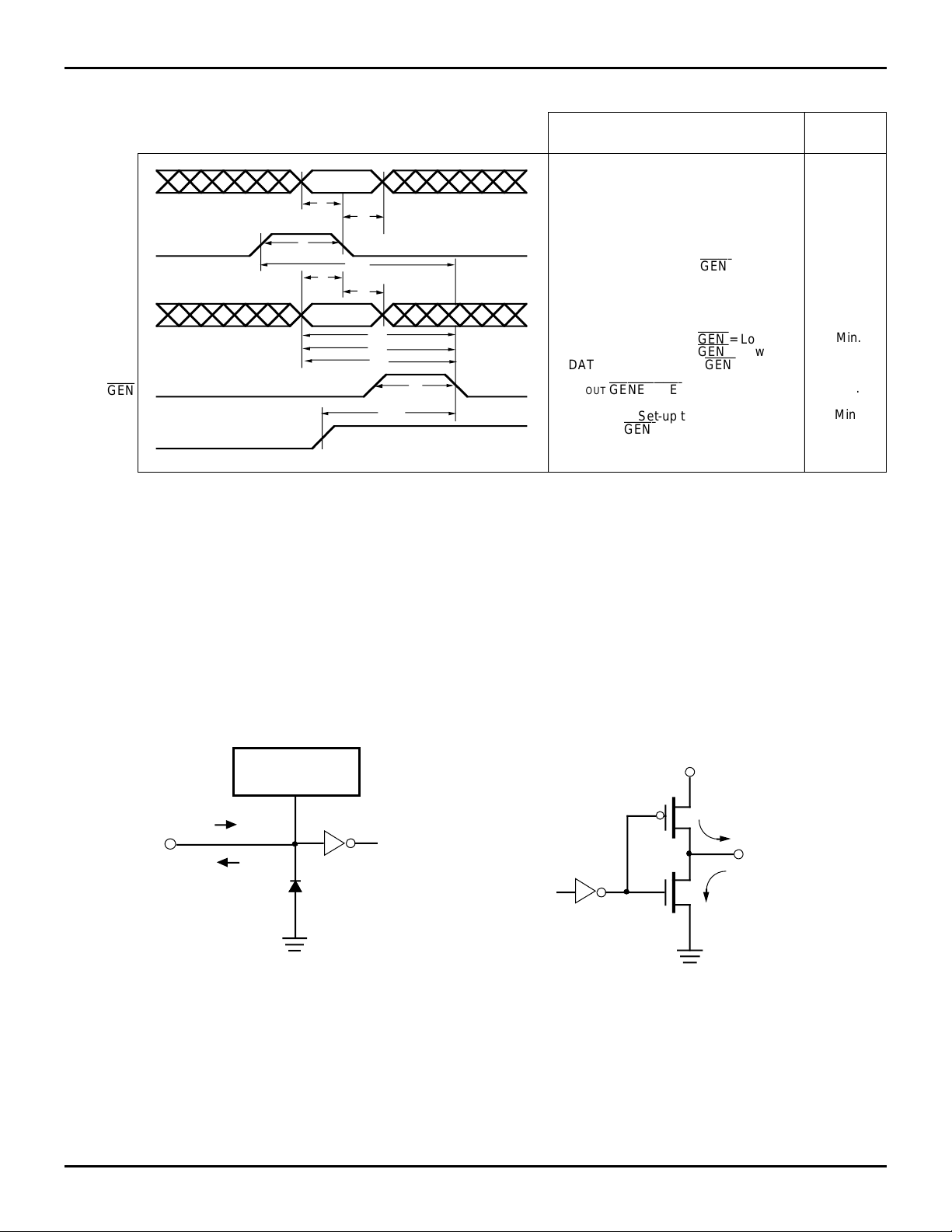
IDT49C460/A/B/C/D/E
32-BIT CMOS ERROR DETECTION AND CORRECTION UNIT MILITARY AND COMMERCIAL TEMPERATURE RANGES
SET-UP AND HOLD TIMES AND MINIMUM PULSE WIDTHS
CBIN
LE
DATA
LE
OUT/
GEN
CORRECT
IN.
IN
CODE ID1,0 = 00, 11
CODE ID1,0 = 10
Of
Valid
2
3
5
14*
3
3
Valid
11
6
6
5
6
CBIN Set-up to LEIN = Low
IN Hold to LEIN = Low
CB
IN width
LE
*LEIN = High to LEOUT/
DATA Set-up to LE
DATA Hold to LE
IN Set-up to LEOUT/
CB
IN Set-up to LEOUT/
CB
DATA Set-up to LE
LE
OUT/
GENERATE
CORRECT Set-up to
LE
OUT/
With Respect To
IN = Low
GEN
= Low
GEN
IN = Low
GEN
GEN
OUT/
GEN
Width
= Low*
= Low
= Low
= Low
Set-up/Hold Time
Min./Max.
Min.
Min.
Min.
Min.
Min.
Min.
Min.
Min.
Min.
Min.
Min.
NOTES: 2584 drw 11
1. BOLD indicates critical parameters.
2. This is "E" version timing spec. Check appropriate table for other speed versions.
* Enable to enable timing requirement to ensure that the last DATA word applied to "DATA
is valid at least 4ns before "LE
IN" goes high.
IN" is made available as DATAOUT"; assumes that "DATAIN"
INPUT/OUTPUT INTERFACE CIRCUIT
ESD
PROTECTION
I
IH
INPUTS
I
IL
2584 drw 12
Figure 5. Input Structure (All Inputs)
VCC
IOH
OUTPUTS
IOL
2584 drw 13
Figure 6. Out put Structure
11.6 31

IDT49C460/A/B/C/D/E
32-BIT CMOS ERROR DETECTION AND CORRECTION UNIT MILITARY AND COMMERCIAL TEMPERATURE RANGES
TEST LOAD CIRCUIT
VCC
VIN
Pulse
Generator
D.U.T.
RT
DEFINITIONS:
L = Load capacitance: includes jig and probe capacitance
C
L = Termination resistance: should be equal to ZOUT of the Pulse Generator
R
Figure 7.
AC TEST CONDITIONS
Input Pulse Levels GND to 3.0V
Input Rise/Fall Times 1V/ns
Input Timing Reference Levels 1.5V
Output Reference Levels 1.5V
Output Load See Figure 7
2584 tbl 69
+ 7.0V
500Ω
VOUT
50pF
CL
500Ω
2584 drw 14
Test Switch
Disable Low Closed
Enable Low
All other Tests Open
2584 tbl 68
ORDERING INFORMATION
IDT
49C460
Device TypeXSpeedXPackage
X
Process/
Temperature
Range
BLANK
B
Commercial (0
Military (– 55
Compliant to MIL-STD-883, Class B
G
J
FF
Blank
A
B
C
D
E
Pin Grid Array
Plastic Leaded Chip Carrier
Fine Pitch Flatpack
Standard Speed
High-Speed
Very High-Speed
Super-High-Speed
Ultra-High Speed
Fastest Speed
49C460 32-Bit E. D. C.
°
C to + 70°C)
°
C to + 125°C)
2584 drw 15
11.6 32
 Loading...