

ICT LM340A-24, LM340 Datasheet
LM340/LM78XX Series
3-Terminal Positive Regulators
General Description
The LM140/LM340A/LM340/LM7800C monolithic 3-terminal
positive voltage regulators employ internal current-limiting,
thermal shutdown and safe-area compensation, making
them essentially indestructible. If adequate heat sinking is
provided, theycan deliver over 1.0A output current. They are
intended as fixed voltage regulators in a wide range of
applications including local (on-card) regulation for elimination of noise and distribution problems associated with
single-point regulation. In addition to use as fixed voltage
regulators, these devices can be used with external components to obtain adjustable output voltages and currents.
Considerable effort was expended to make the entire series
of regulators easy to use and minimize the number of external components. It is not necessary to bypass the output,
although this does improve transient response. Input bypassing is needed only if the regulator is located far from the
filter capacitor of the power supply.
The 5V, 12V, and 15V regulator options are available in the
steel TO-3 power package. The LM340A/LM340/LM7800C
series is available in the TO-220 plastic power package, and
the LM340-5.0 is available in the SOT-223 package, as well
as the LM340-5.0 and LM340-12 in the surface-mount
TO-263 package.
Features
n Complete specifications at 1A load
n Output voltage tolerances of
±
2% at Tj= 25˚C and±4%
over the temperature range (LM340A)
n Line regulation of 0.01% of V
OUT
/V of ∆VINat 1A load
(LM340A)
n Load regulation of 0.3% of V
OUT
/A (LM340A)
n Internal thermal overload protection
n Internal short-circuit current limit
n Output transistor safe area protection
n P
+
Product Enhancement tested
Device
Output
Voltages
Packages
LM140 5, 12, 15 TO-3 (K)
LM340A/LM340 5, 12, 15 TO-3 (K), TO-220 (T),
SOT-223 (MP), TO-263 (S)
(5V and 12V only)
LM7800C 5, 8, 12,15TO-220 (T)
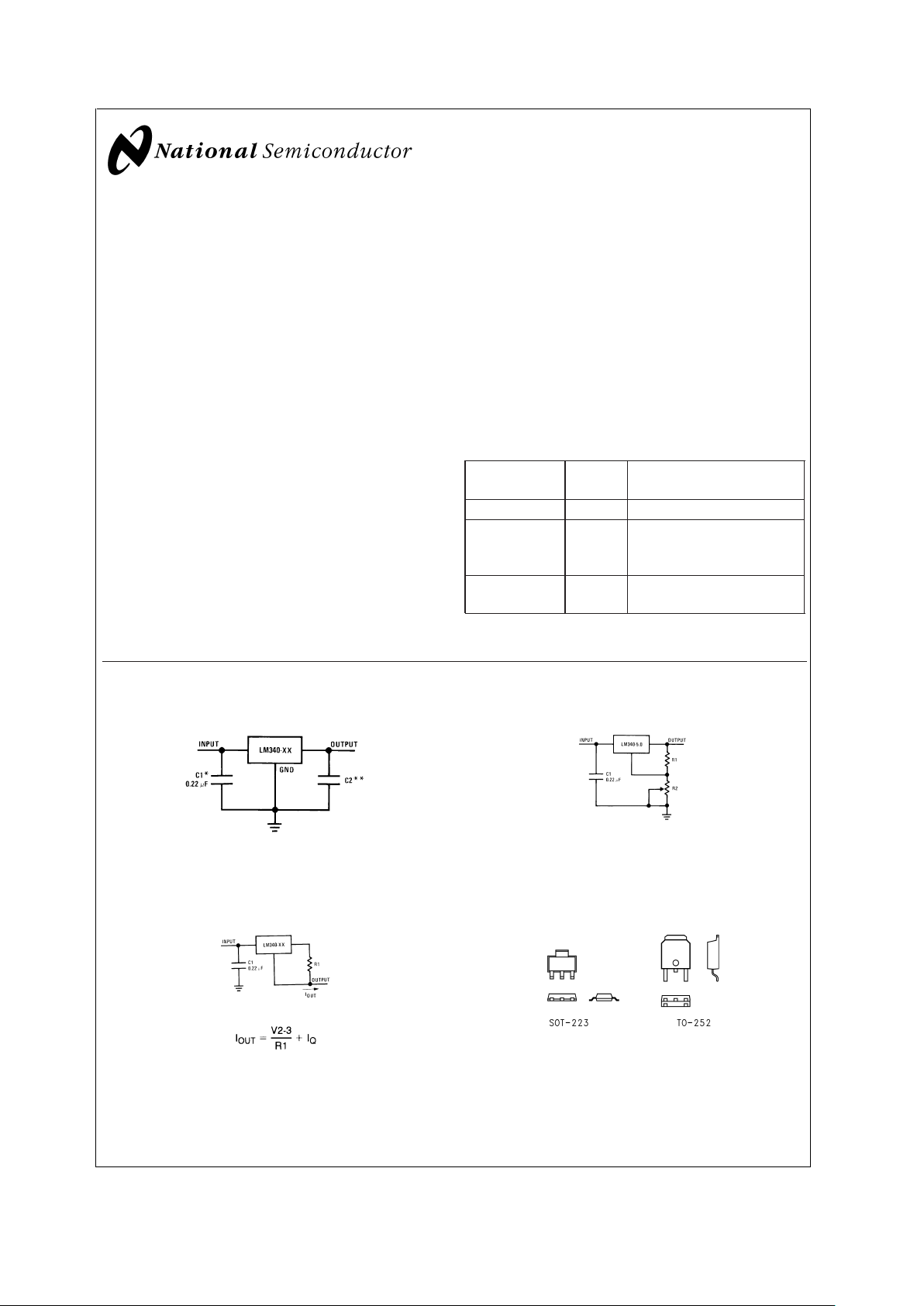
Typical Applications
Fixed Output Regulator Adjustable Output Regulator
00778101
*
Required if the regulator is located far from the power supply filter.
**
Although no output capacitor is needed for stability, it does help transient
response. (If needed, use 0.1 µF, ceramic disc).
00778102
V
OUT
= 5V + (5V/R1 + IQ) R2 5V/R1>3IQ,
load regulation (L
r
) ≈ [(R1 + R2)/R1] (Lrof LM340-5).
Current Regulator
Comparison between SOT-223 and D-Pak (TO-252)
Packages
00778103
∆IQ= 1.3 mA over line and load changes.
00778138
Scale 1:1
September 2001
LM340/LM78XX Series 3-Terminal Positive Regulators
© 2001 National Semiconductor Corporation DS007781 www.national.com
Absolute Maximum Ratings (Note 1)
If Military/Aerospace specified devices are required,
please contact the National Semiconductor Sales Office/
Distributors for availability and specifications.
(Note 5)
DC Input Voltage
All Devices except
LM7824/LM7824C 35V
LM7824/LM7824C 40V
Internal Power Dissipation (Note 2) Internally Limited
Maximum Junction Temperature 150˚C
Storage Temperature Range −65˚C to +150˚C
Lead Temperature (Soldering, 10 sec.)
TO-3 Package (K) 300˚C
TO-220 Package (T), TO-263
Package (S) 230˚C
ESD Susceptibility (Note 3) 2 kV
Operating Conditions (Note 1)
Temperature Range (T
A
) (Note 2)
LM140A, LM140 −55˚C to +125˚C
LM340A, LM340, LM7805C,
LM7812C, LM7815C, LM7808C 0˚C to +125˚C
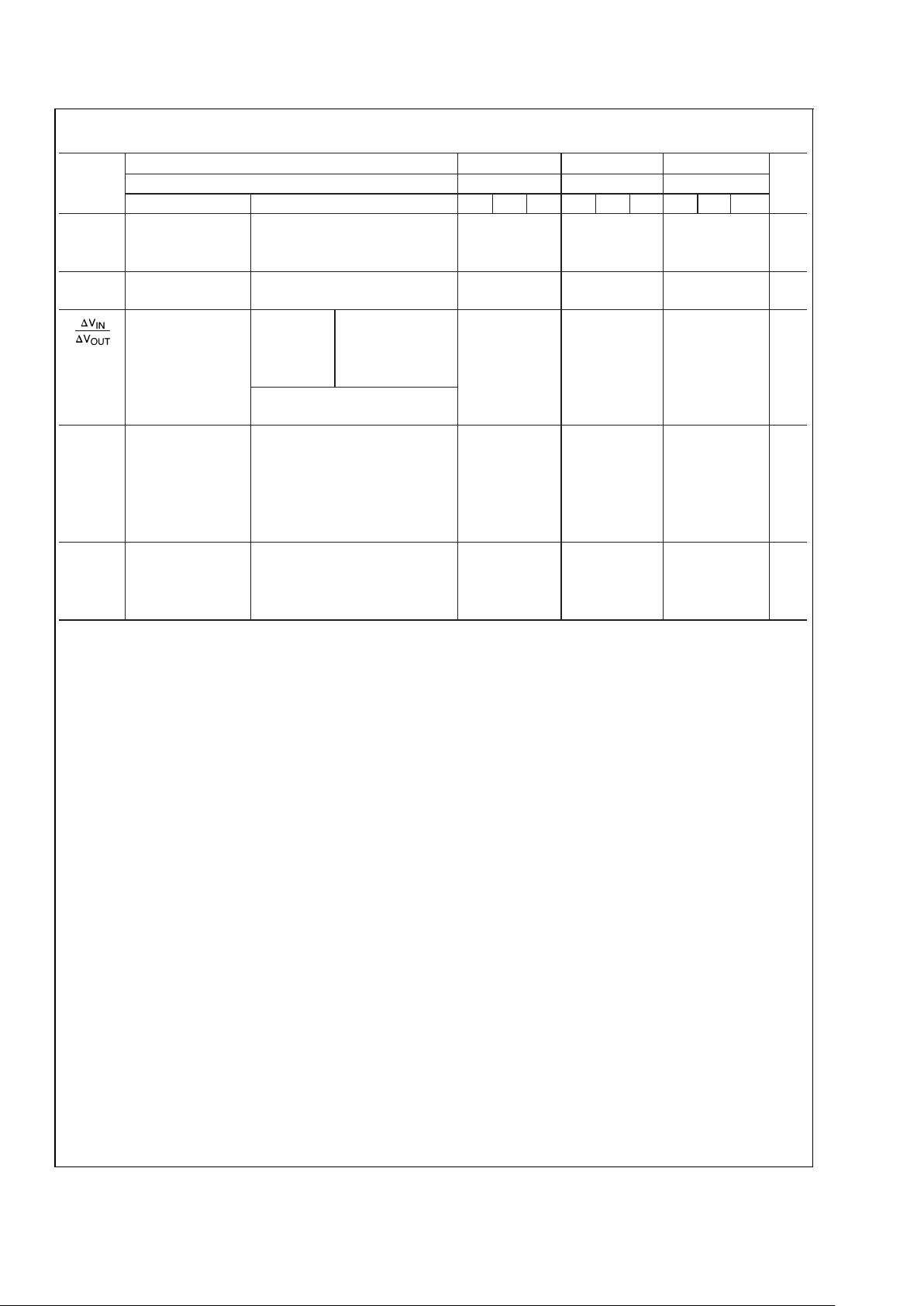
LM340A Electrical Characteristics
I
OUT
= 1A, −55˚C ≤ TJ≤ +150˚C (LM140A), or 0˚C ≤ TJ≤ + 125˚C (LM340A) unless otherwise specified (Note 4)
Output Voltage 5V 12V 15V
Symbol Input Voltage (unless otherwise noted) 10V 19V 23V Units
Parameter Conditions Min Typ Max Min Typ Max Min Typ Max
V
O
Output Voltage TJ= 25˚C 4.9 5 5.1 11.75 12 12.25 14.7 15 15.3 V
P
D
≤ 15W, 5 mA ≤ IO≤ 1A 4.8 5.2 11.5 12.5 14.4 15.6 V
V
MIN
≤ VIN≤ V
MAX
(7.5 ≤ VIN≤ 20) (14.8 ≤ VIN≤ 27) (17.9 ≤ VIN≤ 30) V
∆V
O
Line Regulation IO= 500 mA 10 18 22 mV
∆V
IN
(7.5 ≤ VIN≤ 20) (14.8 ≤ VIN≤ 27) (17.9 ≤ VIN≤ 30) V
T
J
= 25˚C 3 10 4 18 4 22 mV
∆V
IN
(7.5 ≤ VIN≤ 20) (14.5 ≤ VIN≤ 27) (17.5 ≤ VIN≤ 30) V
T
J
= 25˚C 4 9 10 mV
Over Temperature 12 30 30 mV
∆V
IN
(8 ≤ VIN≤ 12) (16 ≤ VIN≤ 22) (20 ≤ VIN≤ 26) V
∆V
O
Load Regulation TJ= 25˚C 5 mA ≤ IO≤ 1.5A 10 25 12 32 12 35 mV
250 mA ≤ I
O
≤ 750
mA
15 19 21 mV
Over Temperature, 25 60 75 mV
5mA≤I
O
≤1A
I
Q
Quiescent
Current
TJ= 25˚C 6 6 6 mA
Over Temperature 6.5 6.5 6.5 mA
∆I
Q
Quiescent
Current
5mA≤IO≤1A 0.5 0.5 0.5 mA
Change T
J
= 25˚C, IO= 1A 0.8 0.8 0.8 mA
V
MIN
≤ VIN≤ V
MAX
(7.5 ≤ VIN≤ 20) (14.8 ≤ VIN≤ 27) (17.9 ≤ VIN≤ 30) V
I
O
= 500 mA 0.8 0.8 0.8 mA
V
MIN
≤ VIN≤ V
MAX
(8 ≤ VIN≤ 25) (15 ≤ VIN≤ 30) (17.9 ≤ VIN≤ 30) V
V
N
Output Noise
Voltage
TA= 25˚C, 10 Hz ≤ f ≤ 100 kHz 40 75 90 µV
Ripple Rejection TJ= 25˚C, f = 120 Hz, IO=1A688061726070dB
or f = 120 Hz, I
O
= 500 mA, 68 61 60 dB
Over Temperature,
V
MIN
≤ VIN≤ V
MAX
(8 ≤ VIN≤ 18) (15 ≤ VIN≤ 25) (18.5 ≤ VIN≤
28.5)
V
R
O
Dropout Voltage TJ= 25˚C, IO= 1A 2.0 2.0 2.0 V
Output
Resistance
f=1kHz 8 18 19 mΩ
LM340/LM78XX
www.national.com 2
LM340A Electrical Characteristics (Continued)
I
OUT
= 1A, −55˚C ≤ TJ≤ +150˚C (LM140A), or 0˚C ≤ TJ≤ + 125˚C (LM340A) unless otherwise specified (Note 4)
Output Voltage 5V 12V 15V
Symbol Input Voltage (unless otherwise noted) 10V 19V 23V Units
Parameter Conditions Min Typ Max Min Typ Max Min Typ Max
Short-Circuit
Current
T
J
= 25˚C 2.1 1.5 1.2 A
Peak Output
Current
T
J
= 25˚C 2.4 2.4 2.4 A
Average TC of
V
O
Min, TJ= 0˚C, IO= 5 mA −0.6 −1.5 −1.8 mV/˚C
V
IN
Input Voltage TJ= 25˚C
Required to
Maintain
7.5 14.5 17.5 V
Line Regulation
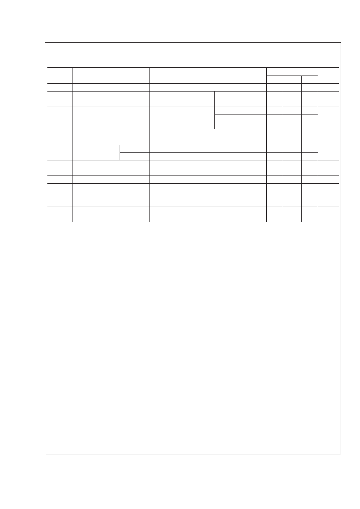
LM140 Electrical Characteristics (Note 4)
−55˚C ≤ TJ≤ +150˚C unless otherwise specified
Output Voltage 5V 12V 15V
Symbol Input Voltage (unless otherwise noted) 10V 19V 23V Units
Parameter Conditions Min Typ Max Min Typ Max Min Typ Max
V
O
Output Voltage TJ= 25˚C, 5 mA ≤ IO≤ 1A 4.8 5 5.2 11.5 12 12.5 14.4 15 15.6 V
P
D
≤ 15W, 5 mA ≤ IO≤ 1A 4.75 5.25 11.4 12.614.25 15.75 V
V
MIN
≤ VIN≤ V
MAX
(8 ≤ VIN≤ 20) (15.5 ≤ VIN≤ 27) (18.5 ≤ VIN≤
30)
V
∆V
O
Line Regulation IO= 500 mA TJ= 25˚C 3 50 4 120 4 150 mV
∆V
IN
(7 ≤ VIN≤ 25) (14.5 ≤ VIN≤ 30) (17.5 ≤ VIN≤
30)
V
−55˚C ≤ T
J
≤ +150˚C 50 120 150 mV
∆V
IN
(8 ≤ VIN≤ 20) (15 ≤ VIN≤ 27) (18.5 ≤ VIN≤
30)
V
I
O
≤ 1A TJ= 25˚C 50 120 150 mV
∆V
IN
(7.5 ≤ VIN≤ 20) (14.6 ≤ VIN≤ 27) (17.7 ≤ VIN≤
30)
V
−55˚C ≤ T
J
≤ +150˚C 25 60 75 mV
∆V
IN
(8 ≤ VIN≤ 12) (16 ≤ VIN≤ 22) (20 ≤ VIN≤ 26) V
∆V
O
Load Regulation TJ= 25˚C 5 mA ≤ IO≤ 1.5A 10 50 12 120 12 150 mV
250 mA ≤ I
P
≤ 750
mA
25 60 75 mV
−55˚C ≤ T
J
≤ +150˚C, 50 120 150 mV
5mA≤I
O
≤1A
I
Q
Quiescent Current IO≤ 1A TJ= 25˚C 6 6 6 mA
−55˚C ≤ T
J
≤ +150˚C 7 7 7 mA
∆I
Q
Quiescent Current 5 mA ≤ IO≤ 1A 0.5 0.5 0.5 mA
Change T
J
= 25˚C, IO≤ 1A 0.8 0.8 0.8 mA
V
MIN
≤ VIN≤ V
MAX
(8 ≤ VIN≤ 20) (15 ≤ VIN≤ 27) (18.5 ≤ VIN≤
30)
V
I
O
= 500 mA, −55˚C ≤ TJ≤ +150˚C 0.8 0.8 0.8 mA
V
MIN
≤ VIN≤ V
MAX
(8 ≤ VIN≤ 25) (15 ≤ VIN≤ 30) (18.5 ≤ VIN≤
30)
V
V
N
Output Noise
Voltage
TA= 25˚C, 10 Hz ≤ f ≤ 100 kHz 40 75 90 µV
LM340/LM78XX
www.national.com3
LM140 Electrical Characteristics (Note 4) (Continued)
−55˚C ≤ TJ≤ +150˚C unless otherwise specified
Output Voltage 5V 12V 15V
Symbol Input Voltage (unless otherwise noted) 10V 19V 23V Units
Parameter Conditions Min Typ Max Min Typ Max Min Typ Max
Ripple Rejection IO≤ 1A, TJ= 25˚Cor68 80 61 72 60 70 dB
f = 120 Hz I
O
≤ 500 mA, 68 61 60 dB
−55˚C ≤ T
J
≤+150˚C
V
MIN
≤ VIN≤ V
MAX
(8 ≤ VIN≤ 18) (15 ≤ VIN≤ 25) (18.5 ≤ VIN≤
28.5)
V
R
O
Dropout Voltage TJ= 25˚C, IO= 1A 2.0 2.0 2.0 V
Output Resistance f = 1 kHz 8 18 19 mΩ
Short-Circuit
Current
T
J
= 25˚C 2.1 1.5 1.2 A
Peak Output
Current
T
J
= 25˚C 2.4 2.4 2.4 A
Average TC of
V
OUT
0˚C ≤ TJ≤ +150˚C, IO= 5 mA −0.6 −1.5 −1.8 mV/˚C
V
IN
Input Voltage TJ= 25˚C, IO≤ 1A
Required to
Maintain
7.5 14.6 17.7 V
Line Regulation
LM340/LM7800C Electrical Characteristics (Note 4)
0˚C ≤ TJ≤ +125˚C unless otherwise specified
Output Voltage 5V 12V 15V
Symbol Input Voltage (unless otherwise noted) 10V 19V 23V Units
Parameter Conditions Min Typ Max Min Typ Max Min Typ Max
V
O
Output Voltage TJ= 25˚C, 5 mA ≤ IO≤ 1A 4.8 5 5.2 11.5 12 12.5 14.4 15 15.6 V
P
D
≤ 15W, 5 mA ≤ IO≤ 1A 4.75 5.25 11.4 12.6 14.25 15.75 V
V
MIN
≤ VIN≤ V
MAX
(7.5 ≤ VIN≤ 20) (14.5 ≤ VIN≤
27)
(17.5 ≤ VIN≤ 30) V
∆V
O
Line Regulation IO= 500 mA TJ= 25˚C 3 50 4 120 4 150 mV
∆V
IN
(7 ≤ VIN≤ 25) (14.5 ≤ VIN≤
30)
(17.5 ≤ VIN≤ 30) V
0˚C ≤ T
J
≤ +125˚C 50 120 150 mV
∆V
IN
(8 ≤ VIN≤ 20) (15 ≤ VIN≤ 27) (18.5 ≤ VIN≤ 30) V
I
O
≤ 1A TJ= 25˚C 50 120 150 mV
∆V
IN
(7.5 ≤ VIN≤ 20) (14.6 ≤ VIN≤
27)
(17.7 ≤ VIN≤ 30) V
0˚C ≤ T
J
≤ +125˚C 25 60 75 mV
∆V
IN
(8 ≤ VIN≤ 12) (16 ≤ VIN≤ 22) (20 ≤ VIN≤ 26) V
∆V
O
Load Regulation TJ= 25˚C 5 mA ≤ IO≤ 1.5A 10 50 12 120 12 150 mV
250 mA ≤ I
O
≤ 750 mA 25 60 75 mV
5mA≤I
O
≤1A, 0˚C ≤ TJ≤
+125˚C
50 120 150 mV
I
Q
Quiescent Current IO≤ 1A TJ= 25˚C 8 8 8 mA
0˚C ≤ T
J
≤ +125˚C 8.5 8.5 8.5 mA
∆I
Q
Quiescent Current 5 mA ≤ IO≤ 1A 0.5 0.5 0.5 mA
Change T
J
= 25˚C, IO≤ 1A 1.0 1.0 1.0 mA
V
MIN
≤ VIN≤ V
MAX
(7.5 ≤ VIN≤ 20) (14.8 ≤ VIN≤
27)
(17.9 ≤ VIN≤ 30) V
LM340/LM78XX
www.national.com 4
LM340/LM7800C Electrical Characteristics (Note 4) (Continued)
0˚C ≤ TJ≤ +125˚C unless otherwise specified
Output Voltage 5V 12V 15V
Symbol Input Voltage (unless otherwise noted) 10V 19V 23V Units
Parameter Conditions Min Typ Max Min Typ Max Min Typ Max
I
O
≤ 500 mA, 0˚C ≤ TJ≤ +125˚C 1.0 1.0 1.0 mA
V
MIN
≤ VIN≤ V
MAX
(7 ≤ VIN≤ 25) (14.5 ≤ VIN≤
30)
(17.5 ≤ VIN≤ 30) V
V
N
Output Noise
Voltage
TA= 25˚C, 10 Hz ≤ f ≤ 100 kHz 40 75 90 µV
Ripple Rejection IO≤ 1A, TJ=
25˚C
62 80 55 72 54 70 dB
f = 120 Hz or I
O
≤ 500 mA, 62 55 54 dB
0˚C ≤ T
J
≤ +125˚C
V
MIN
≤ VIN≤ V
MAX
(8 ≤ VIN≤ 18) (15 ≤ VIN≤ 25) (18.5 ≤ VIN≤
28.5)
V
R
O
Dropout Voltage TJ= 25˚C, IO= 1A 2.0 2.0 2.0 V
Output Resistance f = 1 kHz 8 18 19 mΩ
Short-Circuit Current T
J
= 25˚C 2.1 1.5 1.2 A
Peak Output
Current
T
J
= 25˚C 2.4 2.4 2.4 A
Average TC of V
OUT
0˚C ≤ TJ≤ +125˚C, IO= 5 mA −0.6 −1.5 −1.8 mV/˚C
V
IN
Input Voltage TJ= 25˚C, IO≤ 1A
Required to
Maintain
7.5 14.6 17.7 V
Line Regulation
Note 1: Absolute Maximum Ratings are limits beyond which damage to the device may occur. Operating Conditions are conditions under which the device functions
but the specifications might not be guaranteed. For guaranteed specifications and test conditions see the Electrical Characteristics.
Note 2: The maximum allowable power dissipation at any ambient temperature is a function of the maximum junction temperature for operation (T
JMAX
= 125˚C
or 150˚C), the junction-to-ambient thermal resistance (θ
JA
), and the ambient temperature (TA). P
DMAX
=(T
JMAX−TA
)/θJA. If this dissipation is exceeded, the die
temperature will rise above T
JMAX
and the electrical specifications do not apply. If the die temperature rises above 150˚C, the device will go into thermal shutdown.
For the TO-3 package (K, KC), the junction-to-ambient thermal resistance (θ
JA
) is 39˚C/W. When using a heatsink, θJAis the sum of the 4˚C/W junction-to-case
thermal resistance (θ
JC
) of the TO-3 package and the case-to-ambient thermal resistance of the heatsink. For the TO-220 package (T), θJAis 54˚C/W and θJCis
4˚C/W. If SOT-223 is used, the junction-to-ambient thermal resistance is 174˚C/W and can be reduced by a heatsink (see Applications Hints on heatsinking).
If theTO-263 package is used, the thermal resistance can be reduced by increasing the PC board copper area thermally connected to the package: Using 0.5 square
inches of copper area, θ
JA
is 50˚C/W; with 1 square inch of copper area, θJAis 37˚C/W; and with 1.6 or more inches of copper area, θJAis 32˚C/W.
Note 3: ESD rating is based on the human body model, 100 pF discharged through 1.5 kΩ.
Note 4: All characteristics are measured with a 0.22 µF capacitor from input to ground and a 0.1 µF capacitor from output to ground.All characteristics except noise
voltage and ripple rejection ratio are measured using pulse techniques (t
w
≤ 10 ms, duty cycle ≤ 5%). Output voltage changes due to changes in internal temperature
must be taken into account separately.
Note 5: A military RETS specification is available on request. At the time of printing, the military RETS specifications for the LM140AK-5.0/883, LM140AK-12/883,
and LM140AK-15/883 complied with the min and max limits for the respective versions of the LM140A. At the time of printing, the military RETS specifications for
the LM140K-5.0/883, LM140K-12/883, and LM140K-15/883 complied with the min and max limits for the respective versions of the LM140. The LM140H/883,
LM140K/883, and LM140AK/883 may also be procured as a Standard Military Drawing.
LM340/LM78XX
www.national.com5
LM7808C
Electrical Characteristics
0˚C ≤ TJ≤ +150˚C, VI= 14V, IO= 500 mA, CI= 0.33 µF, CO= 0.1 µF, unless otherwise specified
Symbol Parameter Conditions (Note 6) LM7808C Units
Min Typ Max
V
O
Output Voltage TJ= 25˚C 7.7 8.0 8.3 V
∆V
O
Line Regulation TJ= 25˚C 10.5V ≤ VI≤ 25V 6.0 160 mV
11.0V ≤ V
I
≤ 17V 2.0 80
∆V
O
Load Regulation TJ= 25˚C 5.0 mA ≤ IO≤ 1.5A 12 160 mV
250 mA ≤ I
O
≤ 750
mA
4.0 80
V
O
Output Voltage 11.5V ≤ VI≤ 23V, 5.0 mA ≤ IO≤ 1.0A, P ≤ 15W 7.6 8.4 V
I
Q
Quiescent Current TJ= 25˚C 4.3 8.0 mA
∆I
Q
Quiescent With Line 11.5V ≤ VI≤ 25V 1.0 mA
Current Change With Load 5.0 mA ≤ I
O
≤ 1.0A 0.5
V
N
Noise TA= 25˚C, 10 Hz ≤ f ≤ 100 kHz 52 µV
∆V
I
/∆VORipple Rejection f = 120 Hz, IO= 350 mA, TJ= 25˚C 56 72 dB
V
DO
Dropout Voltage IO= 1.0A, TJ= 25˚C 2.0 V
R
O
Output Resistance f = 1.0 kHz 16 mΩ
I
OS
Output Short Circuit Current TJ= 25˚C, VI= 35V 0.45 A
I
PK
Peak Output Current TJ= 25˚C 2.2 A
∆V
O
/∆T Average Temperature IO= 5.0 mA 0.8 mV/˚C
Coefficient of Output Voltage
Note 6: All characteristics are measured with a 0.22 µF capacitor from input to ground and a 0.1 µF capacitor from output to ground.All characteristics except noise
voltage and ripple rejection ratio are measured using pulse techniques (t
w
≤ 10 ms, duty cycle ≤ 5%). Output voltage changes due to changes in internal temperature
must be taken into account separately.
LM340/LM78XX
www.national.com 6
 Loading...