


ICSI IC62VV25616L-100B, IC62VV25616L-100BI, IC62VV25616L-100T, IC62VV25616L-100TI, IC62VV25616L-55B Datasheet
...IC62VV25616L
IC62VV25616LL
Document Title
256Kx16 bit 1.8V and Ultra Low Power CMOS Static RAM
Revision History
Revision No |
History |
Draft Date |
Remark |
0A |
Initial Draft |
November 13,2001 |
Preliminary |
The attached datasheets are provided by ICSI. Integrated Circuit Solution Inc reserve the right to change the specifications and products. ICSI will answer to your questions about device. If you have any questions, please contact the ICSI offices.
Integrated Circuit Solution Inc. |
1 |
LPSR019-0A 11/13/2001
IC62VV25616L
IC62VV25616LL
256K x 16 1.8V ULTRA
LOW POWER CMOS STATIC RAM
FEATURES
•High-speed access times: 55, 70, 100 ns
•CMOS low power operation
ICC1=10mA (typical)* operating
ISB2=1µA (typical)* CMOS standby
*Typical values are measured at VCC=1.8V, TA=25°C
•TTL compatible interface levels
•Single 1.65V-2.2V Vcc power supply
•Fully static operation: no clock or refresh required
•Three state outputs
•Data control for upper and lower bytes
•Industrial temperature available
•Available in the 44-pin TSOP-2 and 48-pin 6*8mm TF-BGA
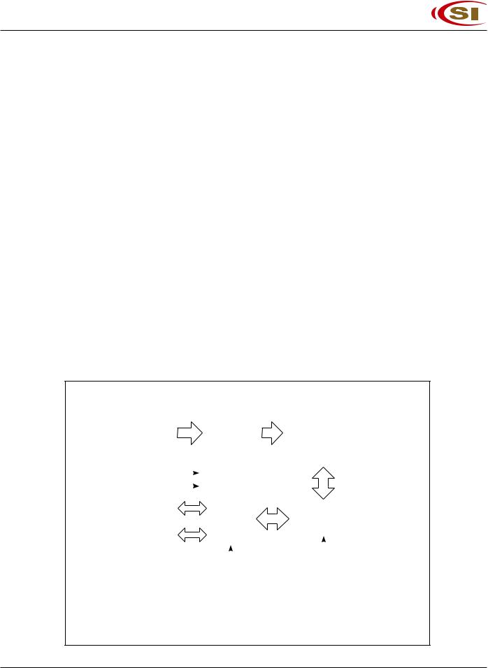
FUNCTIONAL BLOCK DIAGRAM
DESCRIPTION
The ICSI IC62VV25616L and IC62VV25616LL are low-power, 4.194,304 bit static RAMs organized as 262,144 words by 16 bits. They are fabricated using ICSI's high-performance CMOS technology. This highly reliable process coupled with innovative circuit design techniques, yields high-performance and low power consumption devices.
When CE is HIGH (deselected) or both LB and UB are HIGH, the device assumes a standby mode at which the power dissipation can be reduced by using CMOS input levels.
Easy memory expansion is provided by using Chip Enable Output and Enable inputs, CE and OE. The active LOW Write Enable (WE) controls both writing and reading of the memory. A data byte allows Upper Byte (UB) and Lower Byte (LB) access.
The IC62VV25616L and IC62VV25616LL are packaged in the JEDEC standare 44-pin TSOP-2 and 48-pin 6*8mm TF-BGA.
A0-A17 |
|
|
|
|
|
|
|
|
|
|
|
|
|
DECODER |
|
|
256K x 16 |
||||
|
|
|
|
|
|
|
|
|
|
|
|
|
|
|
MEMORY ARRAY |
||||||
|
|
|
|
|
|
|
|
|
|
|
|
|
|
|
|
|
|
|
|||
VCC |
|
|
|
|
|
|
|
|
|
|
|
|
|
|
|
|
|
|
|
|
|
|
|
|
|
|
|
|
|
|
|
|
|
|
|
|
|
|
|
|
|
|
|
|
|
|
|
|
|
|
|
|
|
|
|
|
|
|
|
|
|
|
|
|
|
GND |
|
|
|
|
|
|
|
|
|
|
|
|
|
|
|
|
|
|
|
|
|
|
|
|
|
|
|
|
|
|
|
|
|
|
|
|
|
|
|
|
|
|
|
I/O0-I/O7 |
|
|
|
|
|
|
|
|
|
|
|
|
|
|
|
|
|
|
|
|
|
|
|
|
|
|
|
|
|
|
|
|
|
|
I/O |
|
|
|
|
|
|
||
|
|
|
|
|
|
|
|
|
|
|
|
|
|
|
|
|
|
|
|||
Lower Byte |
|
|
|
|
|
|
|
|
|
|
|
|
|
|
|
COLUMN I/O |
|
||||
|
|
|
|
|
|
|
|
|
|
|
|
|
DATA |
|
|
|
|
||||
|
|
|
|
|
|
|
|
|
|
|
|
|
|
|
|
|
|||||
I/O8-I/O15 |
|
|
|
|
|
|
|
|
|
|
|
|
|
CIRCUIT |
|
|
|
|
|
||
|
|
|
|
|
|
|
|
|
|
|
|
|
|
|
|
|
|
|
|
|
|
Upper Byte |
|
|
|
|
|
|
|
|
|
|
|
|
|
|
|
|
|
|
|
|
|
|
|
|
|
|
|
|
|
|
|
|
|
|
|
|
|
|
|
|
|
|
|
|
|
|
|
|
|
|
|
|
|
|
|
|
|
|
|
|
|
|
|
|
|
|
|
|
|
|
|
|
|
|
|
|
|
|
|
|
|
|
|
|
|
|
|
|
|
|
|
|
|
|
|
|
|
|
|
|
|
|
|
|
|
|
|
||
|
CE |
|
|
|
|
|
|
|
|
|
|||||||||||
|
|
|
|
|
|
|
|
|
|
|
|
|
|
|
|
|
|
|
|||
|
|
|
|
|
|
|
|
|
|
|
|
|
|
|
|
|
|
||||
|
OE |
|
CONTROL |
|
|
|
|
|
|||||||||||||
|
|
|
|
|
|
|
|
|
|
|
|
|
|
||||||||
|
WE |
|
|
|
|
|
|
|
|
|
|||||||||||
|
|
|
|
|
CIRCUIT |
|
|
|
|
|
|||||||||||
|
|
|
|
|
|
|
|
||||||||||||||
|
|
|
|
|
|
|
|
|
|
|
|
|
|
|
|
|
|
|
|||
|
|
|
|
|
UB |
|
|
|
|
|
|
|
|
|
|
|
|
||||
|
|
|
|
|
|
|
|
|
|
|
|
||||||||||
|
|
|
|
|
|
|
|
|
|
|
|
|
|
|
|
||||||
|
|
|
|
|
|
LB |
|
|
|
|
|
|
|
|
|
|
|
|
|||
|
|
|
|
|
|
|
|
|
|
|
|
|
|
||||||||
|
|
|
|
|
|
|
|
|
|
|
|
|
|
|
|
|
|
|
|
|
|
ICSI reserves the right to make changes to its products at any time without notice in order to improve design and supply the best possible product. We assume no responsibility for any errors which may appear in this publication. © Copyright 2001, Integrated Circuit Solution Inc.
2 |
Integrated Circuit Solution Inc. |
LPSR019-0A 11/13/2001

IC62VV25616L
IC62VV25616LL
PIN CONFIGURATIONS
44-Pin TSOP-2 |
|
|
48-Pin TF-BGA (TOP View) |
|
|
||||||
A4 |
1 |
44 |
A5 |
|
|
|
|
|
|
|
|
A3 |
2 |
43 |
A6 |
|
1 |
2 |
3 |
4 |
5 |
6 |
|
A2 |
3 |
42 |
A7 |
|
|||||||
|
|
|
|
|
|
|
|||||
A1 |
4 |
41 |
OE |
A |
|
|
|
|
|
|
|
A0 |
5 |
40 |
UB |
LB |
OE |
A0 |
A1 |
A2 |
N/C |
||
CE |
6 |
39 |
LB |
|
|
|
|
|
|
|
|
I/O0 |
7 |
38 |
I/O15 |
B |
I/O8 |
UB |
A3 |
A4 |
CE |
I/O0 |
|
I/O1 |
8 |
37 |
I/O14 |
|
|
|
|
|
|
|
|
I/O2 |
9 |
36 |
I/O13 |
C |
I/O9 |
I/O10 |
A5 |
A6 |
I/O1 |
I/O2 |
|
I/O3 |
10 |
35 |
I/O12 |
|
|
|
|
|
|
|
|
Vcc |
11 |
34 |
GND |
D |
GND |
I/O11 |
A17 |
A7 |
I/O3 |
Vcc |
|
GND |
12 |
33 |
Vcc |
|
|
|
|
|
|
|
|
I/O4 |
13 |
32 |
I/O11 |
E |
Vcc |
I/O12 |
NC |
A16 |
I/O4 |
GND |
|
I/O5 |
14 |
31 |
I/O10 |
|
|
|
|
|
|
|
|
I/O6 |
15 |
30 |
I/O9 |
F |
I/O14 |
I/O13 |
A14 |
A15 |
I/O5 |
I/O6 |
|
I/O7 |
16 |
29 |
I/O8 |
|
|
|
|
|
|
|
|
WE |
17 |
28 |
NC |
G |
I/O15 |
NC |
A12 |
A13 |
WE |
I/O7 |
|
A16 |
18 |
27 |
A8 |
|
|
|
|
|
|
|
|
A15 |
19 |
26 |
A9 |
H |
NC |
A8 |
A9 |
A10 |
A11 |
NC |
|
A14 |
20 |
25 |
A10 |
||||||||
|
|
|
|
|
|
|
|||||
A13 |
21 |
24 |
A11 |
|
|
|
|
|
|
|
|
A12 |
22 |
23 |
A17 |
|
|
|
|
|
|
|
|
PIN DESCRIPTIONS
A0-A17 |
Address Inputs |
|
|
I/O0-I/O15 |
Data Input/Output |
|
|
CE |
Chip Enable Input |
|
|
OE |
Output Enable Input |
|
|
WE |
Write Enable Input |
|
|
LB |
Lower-byte Control (l/O0-I/O7) |
|
|
UB |
Upper-byte Control (l/O8-I/O15) |
|
|
NC |
No Connection |
|
|
Vcc |
Power |
|
|
GND |
Ground |
|
|
TRUTH TABLE
|
|
|
|
|
|
|
I/O PIN |
|
Mode |
WE |
CE |
OE |
LB |
UB |
I/O0/-I/O7 |
I/O8-I/O15 |
Power |
|
|
|
|
|
|
|
|
|
Not Selected |
X |
H |
X |
X |
X |
High-Z |
High-Z |
Stand by |
|
X |
L |
X |
H |
H |
High-Z |
High-Z |
Stand by |
|
|
|
|
|
|
|
|
|
Output Disabled |
H |
L |
H |
X |
X |
High-Z |
High-Z |
Active |
|
X |
L |
X |
H |
H |
High-Z |
High-Z |
Stand by |
|
|
|
|
|
|
|
|
|
Read |
H |
L |
L |
L |
H |
DOUT |
High-Z |
Active |
|
H |
L |
L |
H |
L |
High-Z |
DOUT |
|
|
H |
L |
L |
L |
L |
DOUT |
DOUT |
|
|
|
|
|
|
|
|
|
|
Write |
L |
L |
X |
L |
H |
DIN |
High-Z |
Active |
|
L |
L |
X |
H |
L |
High-Z |
DIN |
|
|
L |
L |
X |
L |
L |
DIN |
DIN |
|
|
|
|
|
|
|
|
|
|
Integrated Circuit Solution Inc. |
3 |
LPSR019-0A 11/13/2001

IC62VV25616L
IC62VV25616LL
OPERATING RANGE
Range |
Ambient Temperature |
VCC |
Commercial |
0°C to +70°C |
1.65V- 2.2V |
|
|
|
Industrial |
–40°C to +85°C |
1.65V - 2.2V |
|
|
|
ABSOLUTE MAXIMUM RATINGS(1)
Symbol |
Parameter |
Value |
Unit |
VTERM |
Terminal Voltage with Respect to GND |
–0.5 to Vcc + 0.4 |
V |
TBIAS |
Temperature Under Bias |
–40 to +85 |
°C |
|
|
|
|
VCC |
Vcc related to GND |
–0.3 to +4.0 |
V |
|
|
|
|
TSTG |
Storage Temperature |
–65 to +150 |
°C |
PT |
Power Dissipation |
1.0 |
W |
Notes:
1.Stress greater than those listed under ABSOLUTE MAXIMUM RATINGS may cause permanent damage to the device. This is a stress rating only and functional operation of the device at these or any other conditions above those indicated in the operational sections of this specification is not implied. Exposure to absolute maximum rating conditions for extended periods may affect reliability.
DC ELECTRICAL CHARACTERISTICS (Over Operating Range)
Symbol |
Parameter |
Test Conditions |
Min. |
Max. |
Unit |
VOH |
Output HIGH Voltage |
IOH = –0.1 mA |
1.4 |
— |
V |
|
|
|
|
|
|
VOL |
Output LOW Voltage |
IOL = 0.1 mA |
— |
0.2 |
V |
|
|
|
|
|
|
VIH(1) |
Input HIGH Voltage |
|
1.4 |
VCC + 0.2 |
V |
VIL(2) |
Input LOW Voltage |
|
–0.2 |
0.4 |
V |
ILI |
Input Leakage |
GND ≤ VIN ≤ VCC |
–1 |
1 |
µA |
|
|
|
|
|
|
ILO |
Output Leakage |
GND ≤ VOUT ≤ VCC, OUTPUTS DISABLED |
–1 |
1 |
µA |
Notes:
1.VIH(max.) = VCC+2.0V for pulse width less than 10 ns.
2.VIL(min.) = –2.0V for pulse width less than 10 ns.
CAPACITANCE(1)
Symbol |
Parameter |
Conditions |
Max. |
Unit |
CIN |
Input Capacitance |
VIN = 0V |
6 |
pF |
|
|
|
|
|
COUT |
Output Capacitance |
VOUT = 0V |
8 |
pF |
|
|
|
|
|
Notes:
1. Tested initially and after any design or process changes that may affect these parameters.
4 |
Integrated Circuit Solution Inc. |
LPSR019-0A 11/13/2001
 Loading...