


IC61C3216-12K
ICSI IC61C3216-12K, IC61C3216-12T, IC61C3216-12TI, IC61C3216-15K, IC61C3216-15KI Datasheet
...
IC61C3216
Integrated Circuit Solution Inc. 1
AHSR028-0A 10/5/2001
1
2
3
4
5
6
7
8
9
10
11
12
Document Title
32K x 16 Hight Speed SRAM
Revision History
Revision No History Draft Date Remark
0A Initial Draft October 5,2001
The attached datasheets are provided by ICSI. Integrated Circuit Solution Inc reserve the right to change the specifications and
products. ICSI will answer to your questions about device. If you have any questions, please contact the ICSI offices.
IC61C3216
2 Integrated Circuit Solution Inc.
AHSR028-0A 10/5/2001
FEATURES
• High-speed access time: 10, 12, 15, and 20 ns
• CMOS low power operation
— 450 mW (typical) operating
— 250 µW (typical) standby
• TTL compatible interface levels
• Single 5V ± 10% power supply
• I/O compatible with 3.3V device
• Fully static operation: no clock or refresh
required
• Three state outputs
• Industrial temperature available
• Available in 44-pin 400mil SOJ package and
44-pin TSOP-2
32K x 16 HIGH-SPEED CMOS STATIC RAM
DESCRIPTION
The ICSI IC61C3216 is a high-speed, 512K static RAM
organized as 32,768 words by 16 bits. It is fabricated using
ICSI's high-performance CMOS technology. This highly reli-
able process coupled with innovative circuit design techniques,
yields fast access times with low power consumption.
When CE is HIGH (deselected), the device assumes a standby
mode at which the power dissipation can be reduced down with
CMOS input levels.
Easy memory expansion is provided by using Chip Enable and
Output Enable inputs, CE and OE. The active LOW Write
Enable (WE) controls both writing and reading of the memory.
A data byte allows Upper Byte (UB) and Lower Byte (LB)
access.
The IC61C3216 is packaged in the JEDEC standard 44-pin
400mil SOJ and 44-pin 400mil TSOP-2.
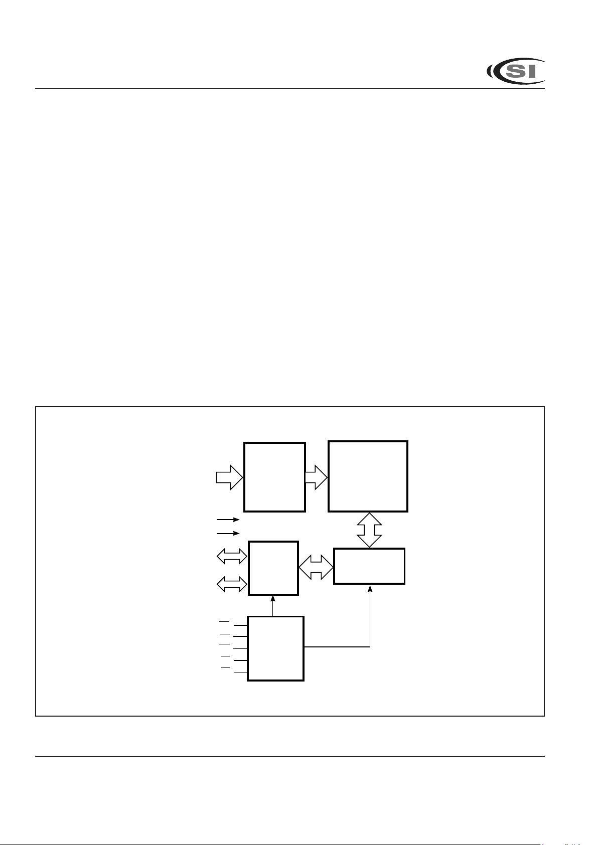
FUNCTIONAL BLOCK DIAGRAM
ICSI reserves the right to make changes to its products at any time without notice in order to improve design and supply the best possible product. We assume no responsibility for any errors
which may appear in this publication. © Copyright 2000, Integrated Circuit Solution Inc.
A0-A14
CE
OE
WE
32K x 16
MEMORY ARRAY
DECODER
COLUMN I/O
CONTROL
CIRCUIT
GND
VCC
I/O
DATA
CIRCUIT
I/O0-I/O7
Lower Byte
I/O8-I/O15
Upper Byte
UB
LB
IC61C3216
Integrated Circuit Solution Inc. 3
AHSR028-0A 10/5/2001
1
2
3
4
5
6
7
8
9
10
11
12
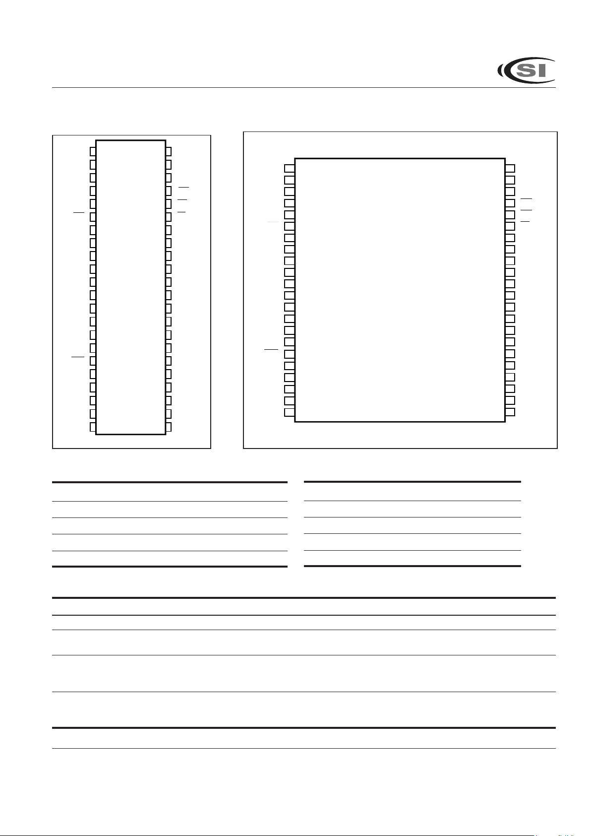
PIN CONFIGURATIONS
44-Pin SOJ
PIN DESCRIPTIONS
A0-A14 Address Inputs
I/O0-I/O15 Data Inputs/Outputs
CE Chip Enable Input
OE Output Enable Input
WE Write Enable Input
1
2
3
4
5
6
7
8
9
10
11
12
13
14
15
16
17
18
19
20
21
22
44
43
42
41
40
39
38
37
36
35
34
33
32
31
30
29
28
27
26
25
24
23
NC
A14
A13
A12
A11
CE
I/O0
I/O1
I/O2
I/O3
Vcc
GND
I/O4
I/O5
I/O6
I/O7
WE
A10
A9
A8
A7
NC
A0
A1
A2
OE
UB
LB
I/O15
I/O14
I/O13
I/O12
GND
Vcc
I/O11
I/O10
I/O9
I/O8
NC
A3
A4
A5
A6
NC
TRUTH TABLE
Mode
WEWE
WEWE
WE
CECE
CECE
CE
OEOE
OEOE
OE
LBLB
LBLB
LB
UBUB
UBUB
UB I/O0-I/O7 I/O8-I/O15 Vcc Current
Not Selected X H X X X High-Z High-Z ISB1, ISB2
Output Disabled H L H X X High-Z High-Z ICC
X L X H H High-Z High-Z
Read H L L L H DOUT High-Z ICC
H L L H L High-Z DOUT
HLLLL DOUT DOUT
Write L L X L H DIN High-Z ICC
L L X H L High-Z DIN
LLXLL DIN DIN
1
2
3
4
5
6
7
8
9
10
11
12
13
14
15
16
17
18
19
20
21
22
44
43
42
41
40
39
38
37
36
35
34
33
32
31
30
29
28
27
26
25
24
23
NC
A14
A13
A12
A11
CE
I/O0
I/O1
I/O2
I/O3
Vcc
GND
I/O4
I/O5
I/O6
I/O7
WE
A10
A9
A8
A7
NC
A0
A1
A2
OE
UB
LB
I/O15
I/O14
I/O13
I/O12
GND
Vcc
I/O11
I/O10
I/O9
I/O8
NC
A3
A4
A5
A6
NC
44-Pin TSOP-2
LB Lower-byte Control (I/O0-I/O7)
UB Upper-byte Control (I/O8-I/O15)
NC No Connection
Vcc Power
GND Ground
 Loading...