

Icom ID-31A, ID-31E Service Manual
UHF TRANSCEIVER
S-14813XZ-C1
Feb. 2012
INTRODUCTION
This service manual describes the latest technical
information for the ID-31A/ID-31E UHF TRANSCEIVER, at
the time of publication.
MODEL VERSION
USA BC-167SA
KOR BC-167SD
ID-31A
ID-31E
EXP BC-167SA
EXP-01 BC-167SD
AUS BC-167SV
EUR BC-167SD
UK N/A
ITR BC-167SD
SUPPLIED
CHARGER
To upgrade quality, any electrical or mechanical parts and
internal circuits are subject to change without notice or
obligation.
CAUTION
NEVER connect the transceiver to an AC outlet or to a DC
power supply that uses more than the specified voltage.
This will ruin the transceiver.
DO NOT expose the transceiver to rain, snow or any liquids.
DO NOT reverse the polarities of the power supply when
connecting the transceiver.
DO NOT apply an RF signal of more than 20 dBm (100 mW) to
the antenna connector. This could damage the transceiver’s
front-end.
ORDERING PARTS
Be sure to include the following four points when ordering
replacement parts:
1. 10-digit Icom part number
2. Component name
3. Equipment model name and unit name
4. Quantity required
<ORDER EXAMPLE>
1110003491 S.IC TA31136FNG ID-31A MAIN UNIT 5 pieces
8820001210 Screw 2438 screw ID-31E Top cover 10 pieces
Addresses are provided on the inside back cover for your
convenience.
(ID-31A)
REPAIR NOTES
1. Make sure that the problem is internal before disassembling the transceiver.
2. DO NOT open the transceiver until the transceiver is
disconnected from its power source.
3. DO NOT force any of the variable components. Turn them
slowly and smoothly.
4. DO NOT short any circuits or electronic parts. An
insulated tuning tool MUST be used for all adjustments.
5. DO NOT keep power ON for a long time when the
transceiver is defective.
6. DO NOT transmit power into a Standard Signal Generator
or a Sweep Generator.
7. ALWAYS connect a 30–40 dB attenuator between the
transceiver and a Deviation Meter or Spectrum Analyzer,
when using such test equipment.
8. READ the instructions of the test equipment throughly
before connecting it to the transceiver.
Icom, Icom Inc. and the Icom logo are registered trademarks of Icom Incorporated (Japan) in Japan, the United States, the
United Kingdom, Germany, France, Spain, Russia and/or other countries.

TABLE OF CONTENTS
SECTION 1 SPECIFICATIONS
SECTION 2 INSIDE VIEWS
SECTION 3 DISASSEMBLY INSTRUCTION
SECTION 4 CIRCUIT DESCRIPITON
4-1 RECEIVER CIRCUITS. . . . . . . . . . . . . . . . . . . . . . . . . . . . . . . . . . . . . . . . . . . . . . . . . . . . . . . . 4-1
4-2 TRANSMITTER CIRCUITS . . . . . . . . . . . . . . . . . . . . . . . . . . . . . . . . . . . . . . . . . . . . . . . . . . . . 4-2
4-3 FREQUENCY SYNTHESIZER CIRCUITS . . . . . . . . . . . . . . . . . . . . . . . . . . . . . . . . . . . . . . . . 4-3
4-4 VOLTAGE DIAGRAM . . . . . . . . . . . . . . . . . . . . . . . . . . . . . . . . . . . . . . . . . . . . . . . . . . . . . . . . . 4-3
4-5 PORT ALLOCATIONS . . . . . . . . . . . . . . . . . . . . . . . . . . . . . . . . . . . . . . . . . . . . . . . . . . . . . . . . 4-4
SECTION 5 ADJUSTMENT PROCEDURES
5-1 PREPARATION . . . . . . . . . . . . . . . . . . . . . . . . . . . . . . . . . . . . . . . . . . . . . . . . . . . . . . . . . . . . . 5-1
5-2 FREQUENCY ADJUSTMENT . . . . . . . . . . . . . . . . . . . . . . . . . . . . . . . . . . . . . . . . . . . . . . . . . . 5-3
5-3 TRANSMIT ADJUSTMENT . . . . . . . . . . . . . . . . . . . . . . . . . . . . . . . . . . . . . . . . . . . . . . . . . . . . 5-3
5-4 RECEIVE ADJUSTMENT . . . . . . . . . . . . . . . . . . . . . . . . . . . . . . . . . . . . . . . . . . . . . . . . . . . . . 5-7
SECTION 6 PARTS LIST
SECTION 7 MECHANICAL PARTS
SECTION 8 BOARD LAYOUTS
SECTION 9 BLOCK DIAGRAM
SECTION 10 VOLTAGE DIAGRAM

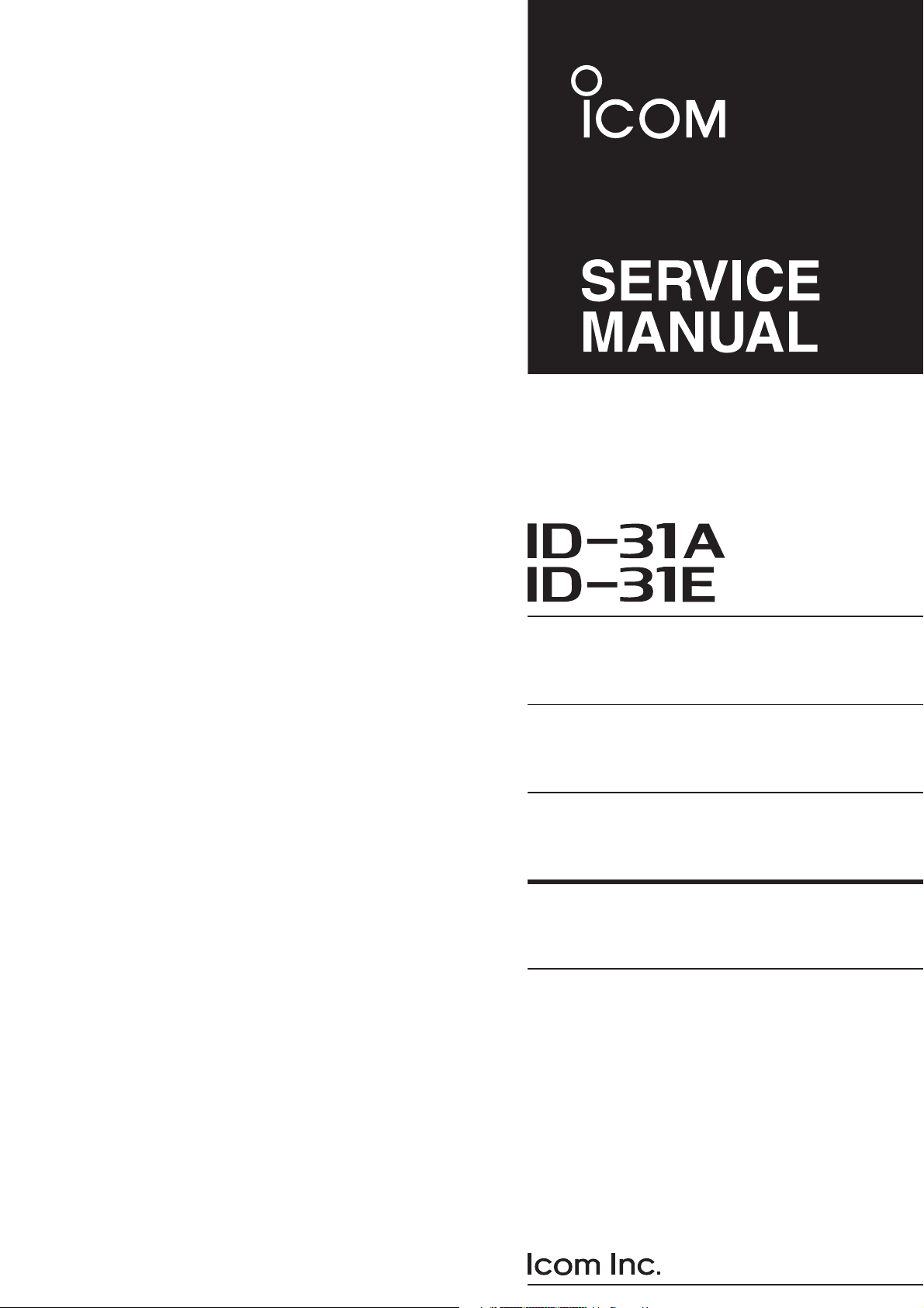
SECTION 1. SPECIFICATIONS
D General
• Frequency coverage : (unit: MHz)
Version
U.S.A. 420–450*
AUS 420–450*
EUR, KOR 430–440 430–440
UK 430–440 400–479*
ITR 430–434, 435–438 430–434, 435–438
EXP 400–479*
EXP-1 430–440 400–479*
*
1
Guaranteed 440–450 MHz only, *2Guaranteed 430–440 MHz only
• Mode :
• No. of memory channels :
• Usable temp. range : –20°C to +60°C; –4°F to +140°F
• Tuning steps : 5, 6.25, 10, 12.5, 15, 20, 25, 30, 50,
• Frequency stability : ±2.5 ppm
• Power supply : 10.0–16.0 V DC for external DC power,
• Digital transmission speed : 4.8 kbps
• Voice coding speed : 2.4 kbps
• Current drain (at 7.4 V DC) :
TX (at 5 W) Less than 2.5A
RX Max. output FM Less than 350 mA (Internal speaker)
Less than 200 mA (External speaker)
DV Less than 450 mA (Internal speaker)
Less than 300 mA (External speaker)
• Antenna connector : SMA (50 Ω)
• Dimensions : 58(W)×95(H)×25.4(D) mm;
(projections not included) 2.3(W)×3.7(H)×1(D) in
• Weight (approximately) : 140 g; 4.94 oz
(
TX RX
1
2
2
400–479*
400–479*
400–479*
1
2
2
2
2
FM, FN-N, DV
552
(incl. 50 scan edges and 2 call channels)
100, 125 and 200 kHz
(–20°C to +60°C; –4°F to +140°F)
or specifi ed Icom’s battery pack
without battery pack/case and ant.
)
D Transmitter
• Modulation system :
FM Variable reactance freq. modulation
DV GMSK reactance freq. modulation
• Output power
(at 7.4 V DC) : High 5.0 W, Mid. 2.5 W, Low 0.5 W,
(Typical) S-Low 0.1 W
• Max. frequency deviation : ±5.0 kHz
(FM wide: approx.)
±2.5 kHz (FM narrow: approx.)
• Spurious emissions : Less than –60 dBc at High/Mid.
Less than –13 dBm at Low/S-Low
• Ext. mic. impedance : 2.2 kΩ
D Receiver
• Receive system : Double-conversion superheterodyne
• Intermediate frequencies : 46.35 MHz (1st IF)
450 kHz (2nd IF)
• Sensitivity
FM
DV (PN9/GMSK 4.8 kbps; BER 1%) Less than –11 dBµ
• Audio output power (at 10% distortion)
Internal speaker : More than 0.4 W with a 16 Ω load
External speaker :
• Selectivity :
FM
FM (Narrow), DV More than 50 dB
• Ext. speaker connector : 3-conductor 3.5(d) mm; (1⁄8˝)/8 Ω
• Spurious and image rejection ratio :
More than 60 dB
• Squelch Sensitivity (threshold, 1 kHz/3.5 kHz Dev.):
Less than –15 dBµ
All stated specifi cations are subject to change without notice or obligation.
(except spurious points):
(1 kHz/3.5 kHz Dev.; 12 dB SINAD) Less than –15 dBµ
More than
(Wide) More than 55 dB
0.2 W with a 8 Ω load
1 - 1
SECTION 2. INSIDE VIEWS
• LOGIC UNIT
(TOP VIEW)
RX/TX LED DRIVER
(Q24)
+3.3 V REGULATOR
(IC11)
BACKUP BATTERY
(For the real time clock)
(BT1)
MIC/VOX AMP
(IC19)
2 - 1

• LOGIC UNIT
(BOTTOM VIEW)
CLOCK OSCILLATOR (For the CPU)
(X2)
GPS MODULE CONTROLLER
(IC1)
DATA LEVEL CONVERTER
(IC21)
EEPROM (For GPS data)
(IC3)
SERIAL DATA INTERFACE
(IC2)
+3.3 V REGULATOR
(IC9)
CPU RESET IC
(IC22)
AF FILTER
(IC12)
ALC IC
(IC14)
DUAL INVERTER GATE
(IC8)
AF SW
(IC16)
MIC GAIN SW
(Q18)
CPU
(IC5)
EEPROM (For the CPU)
(IC7)
CLOCK OSCILLATOR
DSP
(IC18)
SERIAL FLASH MEMORY
(IC20)
CLOCK BUFFER
(For the CODEC)
(IC17)
MicroSD CARD SLOT
(J3)
AF FILTER
(IC13)
DUAL STEP-DOWN COVERTER
(IC10)
REAL TIME CLOCK IC
(IC4)
(For the DSP)
(X3)
CODEC
(IC15)
CLOCK OSCILLATOR
(For the real time clock IC)
(X1)
2 - 2
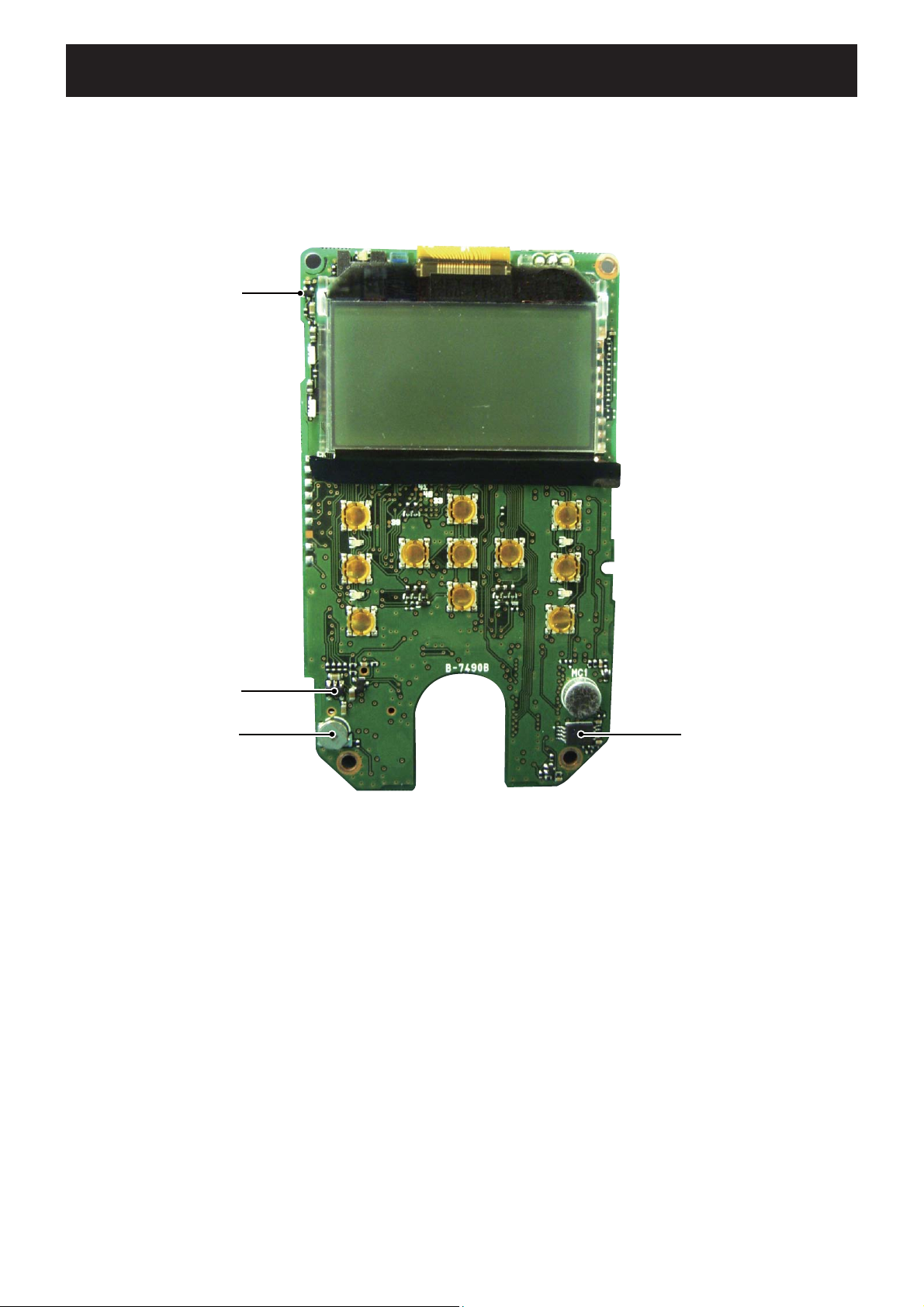
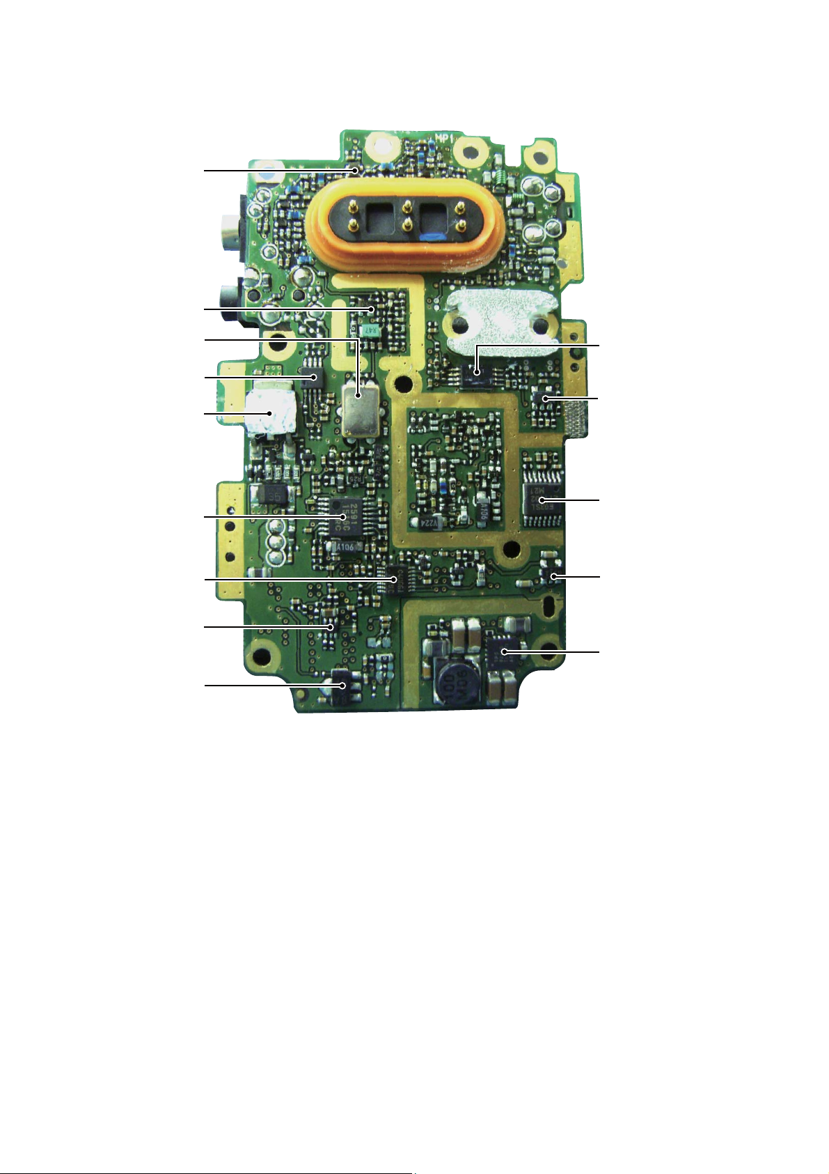
• MAIN UNIT
(TOP VIEW)
CURRENT DETECTION IC
(IC5)
VCC LINE SW
(Q2)
VCC LINE SW
(Q8)
+5 V REGULATOR
(IC1)
POWER AMP
(Q45)
DRIVE AMP
(Q41)
YGR
(Q39)
LOCK VOLTAGE BUFFER
(Q26)
REFERENCE FREQUENCY
OSCILLATOR
(X1)
D/A CONVERTER
(IC11)
+5 V REGULATOR
(IC15)
2ND IF FILTER (For FM mode)
(FI2)
CHARGING LINE SW
(Q7)
2ND IF FILTER
(For DV/FM-N mode)
(FI1)
DISCRIMINATOR
(X2)
AF FILTER
(IC9)
+3 V REGULATOR
(IC10)
2 - 3
RF AMP
(Q47)
• MAIN UNIT
(BOTTOM VIEW)
1ST IF MIXER
(Q46)
1ST IF FILTER
(FI3)
AF POWER AMP
(IC2)
CHARGING LINE DRIVER
(Q6)
IF IC
(IC13)
AF LINE SW
(IC8)
TONE FILTER
(Q31)
AF POWER AMP
REGULATOR
(Q16)
TX POWER SETTING
VOLTAGE BUFFER
(IC14)
BPF TUNING VOLTAGE
BUFFER
(IC12)
PLL
(IC6)
+4 V REGULATOR
(IC3)
STEP-DOWN CONVERTER
(IC4)
2 - 4
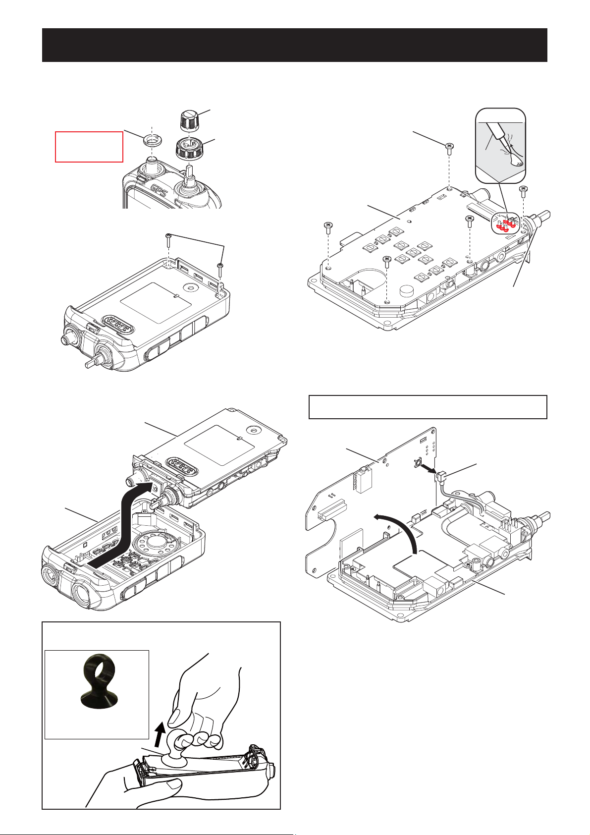
SECTION 3. DISASSEMBLY INSTRUCTION
1. REMOVING THE LOGIC UNIT
1) Remove 2 dials and antenna nut from the front panel.
Inner dial
Antenna nut
Remove with;
“ICOM Driver (Q)”
(8960000370)
Outer dial
2) Remove 2 screws from the bottom of chassis.
Screws
3) Take out the LOGIC UNIT with chassis from the
front panel.
LOGIC UNIT
with chassis
4) Remove 5 screws from the LOGIC UNIT.
5) Unsolder 6 points at the rotary encoder.
UNSOLDER
Screws x5
Solder
remover
LOGIC UNIT
Rotary encoder
6) Separate the LOGIC UNIT from the chassis, and
then disconnect the coaxial cable from the LOGIC
UNIT.
BE CAREFUL about the coaxial cable and connector
when separating the LOGIC UNIT from the chassis.
LOGIC UNIT
J1
Coaxial cable
Front panel
For easy separation of the CHASSIS
Use a suction lifter to lift the bottom of the CHASSIS up.
Suction lifter
• Part name : EA950R-2
• Manufacture : ESCO CO.LTD
Suction lifter
Chassis
3 - 1
(Continued on page 3-2)
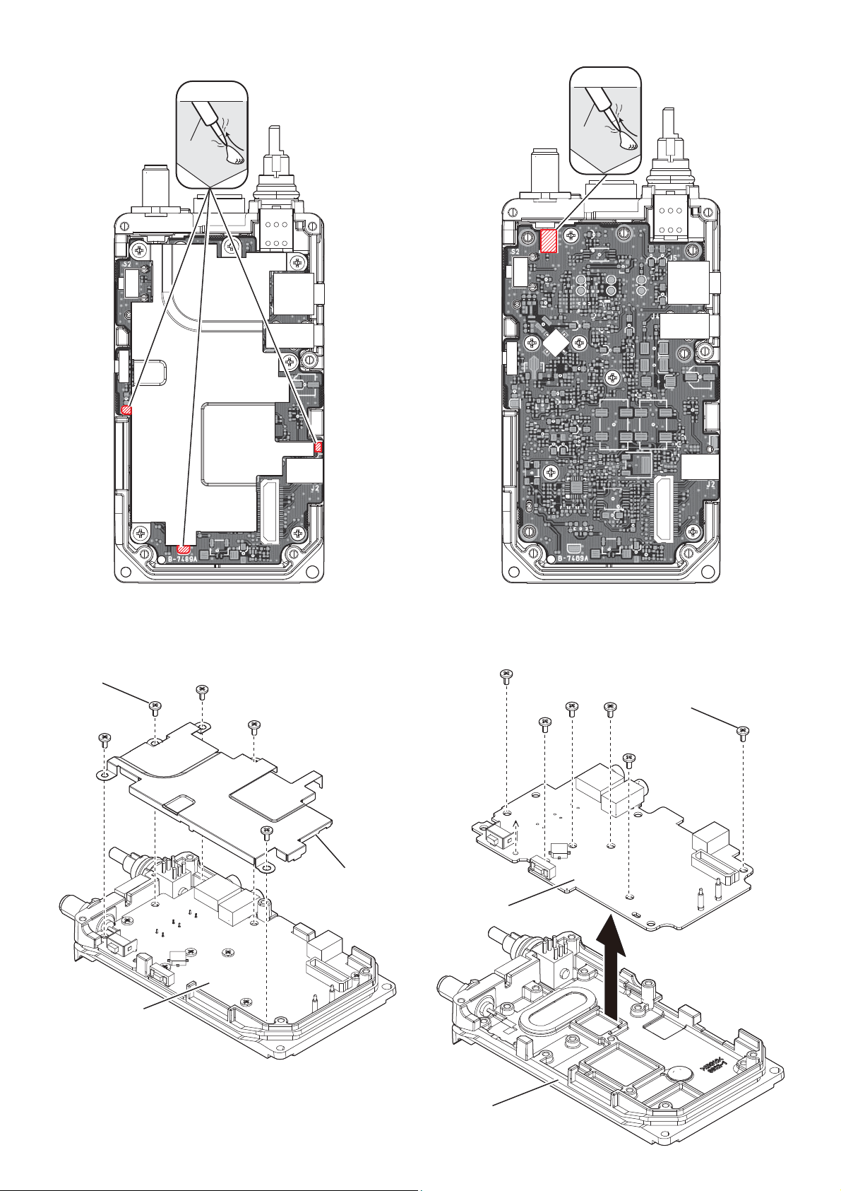
2. REMOVING THE MAIN UNIT
1) Unsolder 3 points on the shield plate.
UNSOLDER
Solder
remover
3) Unsolder a point at the antenna connector.
UNSOLDER
Solder
remover
2) Remove 5 screws from the shield plate, and then
remove it.
Screws x5
Shield plate
MAIN UNIT
4) Remove 6 screws from the MAIN UNIT, and then
remove the MAIN UNIT from the chassis.
Screws x6
MAIN UNIT
3 - 2
Chassis
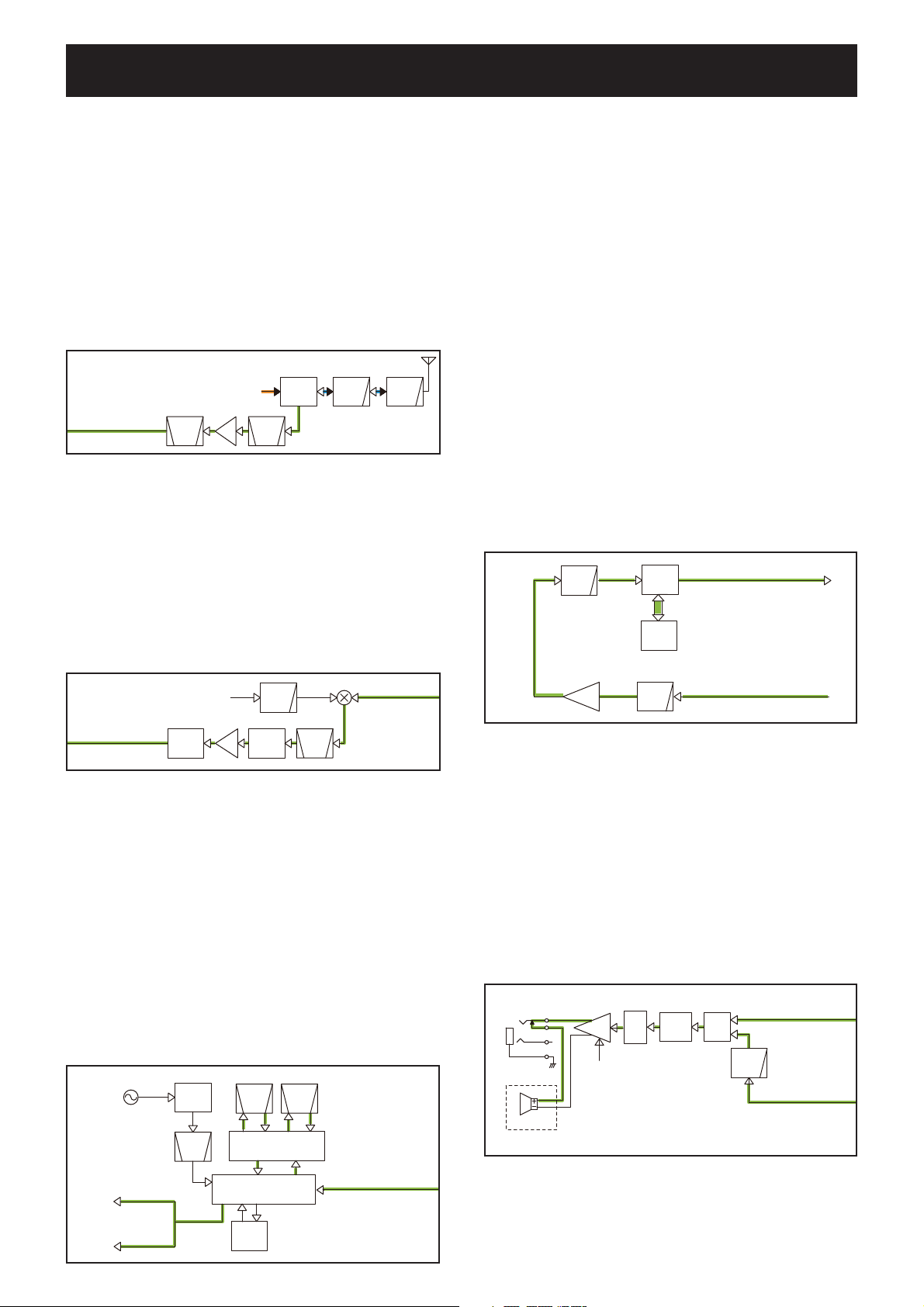
SECTION 4. CIRCUIT DESCRIPTION
4-1 RECEIVE CIRCUITS
RF CIRCUITS (MAIN UNIT)
The RX signal from the antenna is passed through two LPFs
(L32, L34, C302, C303, C306, C307, C312 and L29, C281,
C285), ANT SW (D24, D25, D31, D33, L36, C313, C315,
C319) and tuned BPF (D32, L43, C353), and then applied to
the RF AMP (Q47).
The amplifi ed signal is passed through the tuned BPF (D27, D29,
D30, L28, L31, L33, C286, C290, C292, C293, C297, C299–
C301, C304, C305), and then applied to the 1st IF circuits.
• RF CIRCUITS
D24,D25
D31,D33
From the TX AMP circuits
D27,D29,D30
To the 1st IF circuits
D32
RF
BPF BPF
ANT
SW
LPF
LPF
1ST IF CIRCUITS (MAIN UNIT)
The RX signal from the RF circuits is applied to the 1st IF
mixer (Q46), and mixed with the 1st LO signal from the VCO
(Q27, D10–D12), resulting in the 46.35 MHz 1st IF signal.
The 1st IF signal is passed through the 1st IF fi lter (FI3) and
limiter (D23), and then applied to the 1st IF AMP (Q44). The
amplifi ed signal is passed through another limiter (D22), and
then applied to the 2nd IF circuits.
• 1ST IF CIRCUITS
Q46
From the VCO
To the 2nd IF circuits
LIMIT
Q44
IF
AMP
LIMIT
LPF
1st LO
46.35MHz
XTAL
BPF
FI3D23D22
To the RF circuits
2ND IF CIRCUITS (MAIN UNIT)
The 1st IF signal from the 1st IF circuits is applied to the IF IC
(IC13, pin 16). The IF IC contains the 2nd mixer, 2nd IF AMP,
detector, and so on, in its package.
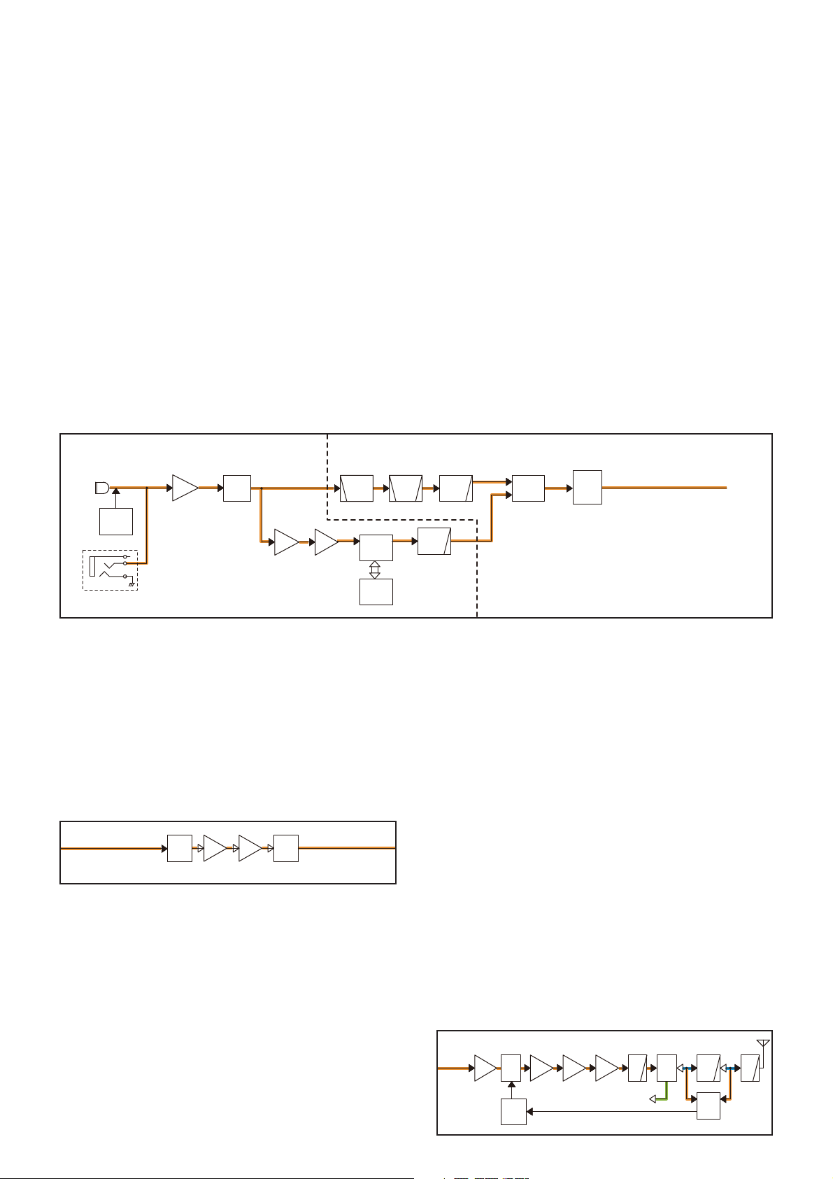
RX AF CIRCUITS (MAIN AND LOGIC UNITS)
• While operating in the DV mode
The demodulated AF signal is passed through the LPF (MAIN
UNIT: R118, R121, C122, C130, C135), and then applied to
the digital demodulation circuits on the LOGIC UNIT.
The AF signal from the MAIN UNIT is amplifi ed by the AF
AMP (LOGIC UNIT: IC13A, pins 1, 2) and passed through the
LPF (LOGIC UNIT: IC13B, pins 6, 7), and then applied to the
liner CODEC (LOGIC UNIT: IC15, pin 3) to be encoded in to
a digital audio signal.
The digital audio signal is demodulated by the DSP (LOGIC
UNIT: IC18), and then applied to the linear codec (LOGIC
UNIT: IC15) to be decoded into an analog audio signal.
The decoded AF signal is applied to the MAIN UNIT.
The AF signal is passed through the mode SW (MAIN UNIT:
IC8, pins 3, 4) and AF fi lters (MAIN UNIT: IC9B, pins 6, 7
and IC9C, pins 9, 10), and then applied to the D/A converter
(MAIN UNIT: IC11, pin 13) to be adjusted in level.
• DIGITAL DEMODULATION CIRCUITS
LPF
IC13B
AMP
IC13A
• While operating in the FM/FM-N mode
The demodulated AF signal is passed through the
C355), mode SW (MAIN UNIT: IC8, pins 1, 2) and AF fi lters
(MAIN UNIT: IC9B, pins 6, 7 and IC9C, pins 9, 10), and then
applied to the D/A converter (MAIN UNIT: IC11, pin 13) to be
adjusted in level.
RTONE
DDET
IC15
IC18
Q31
LINEAR
CODEC
DSP
LPF
To the RX AF circuits
DAFO
From the 2nd IF circuits
LPF (R272,
The 1st IF signal is mixed with the 2nd LO signal from the
reference frequency oscillator (TCXO: X1), resulting in the
450 kHz 2nd IF signal. The 2nd IF signal is passed through
the 2nd IF fi lter (FI1: for DV/FM-N mode, FI2: for FM mode)
to remove sideband noise. The fi ltered signal is amplifi ed by
the 2nd IF AMP, and demodulated by the quadrature detector
with discriminator (X2).
The demodulated AF signal is applied to the RX AF circuits.
• 2ND IF CIRCUITS
X1
15.3MHz
To the digital
demodulation circuits.
To the RX AF circuits
Q38
REF
45.9MHz
X3
BPF
FM-N/DV
CERAMIC
BPF
FI1
DISCRI
X2
W/N
SW
IF IC
FM
CERAMIC
BPF
FI2
Q36,D15
D16,D18,D19
From the 1st IF circuits
IC13
The level-adjusted AF signal is amplifi ed by the AF power
AMP (MAIN UNIT: IC2, pin 1), and then output from the internal speaker (CHASSIS: SP1) or external speaker, through
the SP jack (MAIN UNIT: J4).
• RX AF CIRCUITS
4 - 1
[SP]
J4
SP1
CHASSIS UNIT
VO+
VO-
IC2
AF
AMP
AFON
IC11
IC16
D/A
AF
FILTER
IC9B,C
Q23
From the digital
demodulation circuits.
MODE
SW
IC8
LPF
From the 2nd IF circuits
4-2 TRANSMIT CIRCUITS
TX AF CIRCUITS (LOGIC AND MAIN UNITS)
The AF signal from the internal or external microphone (MIC
signal) is applied to the MIC AMP (LOGIC UNIT: IC19B, pin 5).
• When operating in the DV mode
The amplifi ed signal is passed through the MIC mute SW
(LOGIC UNIT: IC16, pins 1, 7), and then further amplifi ed by
the ALC AMP (LOGIC UNIT: IC14, pin 1). The amplifi ed signal is applied to the liner CODEC (LOGIC UNIT: IC15, pin 2),
through the buffer (LOGIC UNIT: IC12B, pins 6, 7), to be encoded into a digital audio signal.
• When operating in the FM/FM-N mode
The amplifi ed signal is passed through the MIC mute SW
(LOGIC UNIT: IC16, pins 1, 7), and then applied to the MAIN
UNIT.
The MIC signal is passed through the HPF (MAIN UNIT: R78,
C77, C80), BPF (MAIN UNIT: IC9A, pins 1, 3), LPF (MAIN
UNIT: IC9D, pins 13, 14) and mode SW (MAIN UNIT: IC8,
pins 8, 9), and then applied to the D/A converter (MAIN UNIT:
IC11, pin 18) to be adjusted in level.
The digital audio signal is processed by the DSP (LOGIC
UNIT: IC18), and then applied to the linear codec (LOGIC
UNIT: IC15) to be converted into the digital baseband signal.
The digital baseband signal is passed through the LPF (LOGIC
UNIT: IC12A, pins1, 3), and then applied to the MAIN UNIT.
The digital baseband signal is passed through the mode SW
(MAIN UNIT: IC8, pins 10, 11), and then applied to the D/A
converter (MAIN UNIT: IC11, pin 18) to be adjusted in level.
• TX AF CIRCUITS
LOGIC UNIT
MC1
Q18
GAIN
SW
J5
MAIN UNIT
EXTMIC
MIC
AMP
IC19B
IC16
MMUTE
SW
FM mode
DV mode
ALC
AMP
IC14 IC12B
HPF
DMI DMO
BUFF
IC15
LINEAR
CODEC
DSP
IC18
IC9A
MODULATION CIRCUITS (MAIN UNIT)
The MIC signal from the TX AF circuits is applied to the VCO
(Q27, D10–D12) as a modulation signal. The modulation signal is applied to D10 to obtain GMSK (For DV mode) or Frequency Modulation (For FM mode).
The modulated VCO output signal is passed through the buffer (Q30) and amplifi ed by the LO AMP (Q32), and then applied to the TX AMP circuits as the TX signal, through the LO
SW (D14).
• MODULATION CIRCUITS
From the TX AF circuits
Q27,
D10,D11,D12
VCO
BUFF
Q30
LO
AMP
Q32
To the TX AMP circuits
LO
SW
D13,D14
The level-adjusted signal is applied to the modulation circuits.
MAIN UNIT
BPF LPF
IC9D
DMOD
LPF
IC12A
FM
DV
MODE
SW
IC8,Q22
MOD
IC11
To the modulation circuits
D/A
VCOMOD
TX AMP CIRCUITS (MAIN UNIT)
The TX signal is passed through the buffer (Q48) and
attenuator (D20, D21) which controls the TX output power by
the APC AMP (IC14). The TX signal is sequentially amplifi ed
by the YGR (Q39) and drive AMP (Q41), and then passed
through the LPF (L42, C250, C351). The fi ltered TX signal is
applied to the power AMP (Q45).
The amplifi ed TX signal is passed through the LPF (L22, L24,
C260, C265, C267, C270), ANT SW (D24, D25), TX output
power detector (D26, D28) and two LPFs (L29, C281, C285
and L32, L34, C302, C303, C306, C307, C312), before being
applied to the antenna.
APC CIRCUITS (MAIN UNIT)
The voltage produced at the LPFs (L29, C281, C285 and
L32, L34, C302, C303, C306, C307, C312) is rectifi ed by D26
and D28, and it is used as the TX power sensing voltage.
The voltage is applied to the APC AMP (IC14, pin 7), and the
output voltage controls the bias voltages of attenuator (D20,
D21) to keep the TX output power constant.
• TX AMP AND APC CIRCUITS
LPF
D24,D25
D31,D33
ANT
SW
LPFATT
D26,D28
4 - 2
From
the VCO
BUFF
Q48
D20,D21
YGR
AMP
Q39 Q41 Q45
APC
CTRL
IC14B
DRV.
AMP
PWR
AMP
RX circuits
PWR
DET
LPF
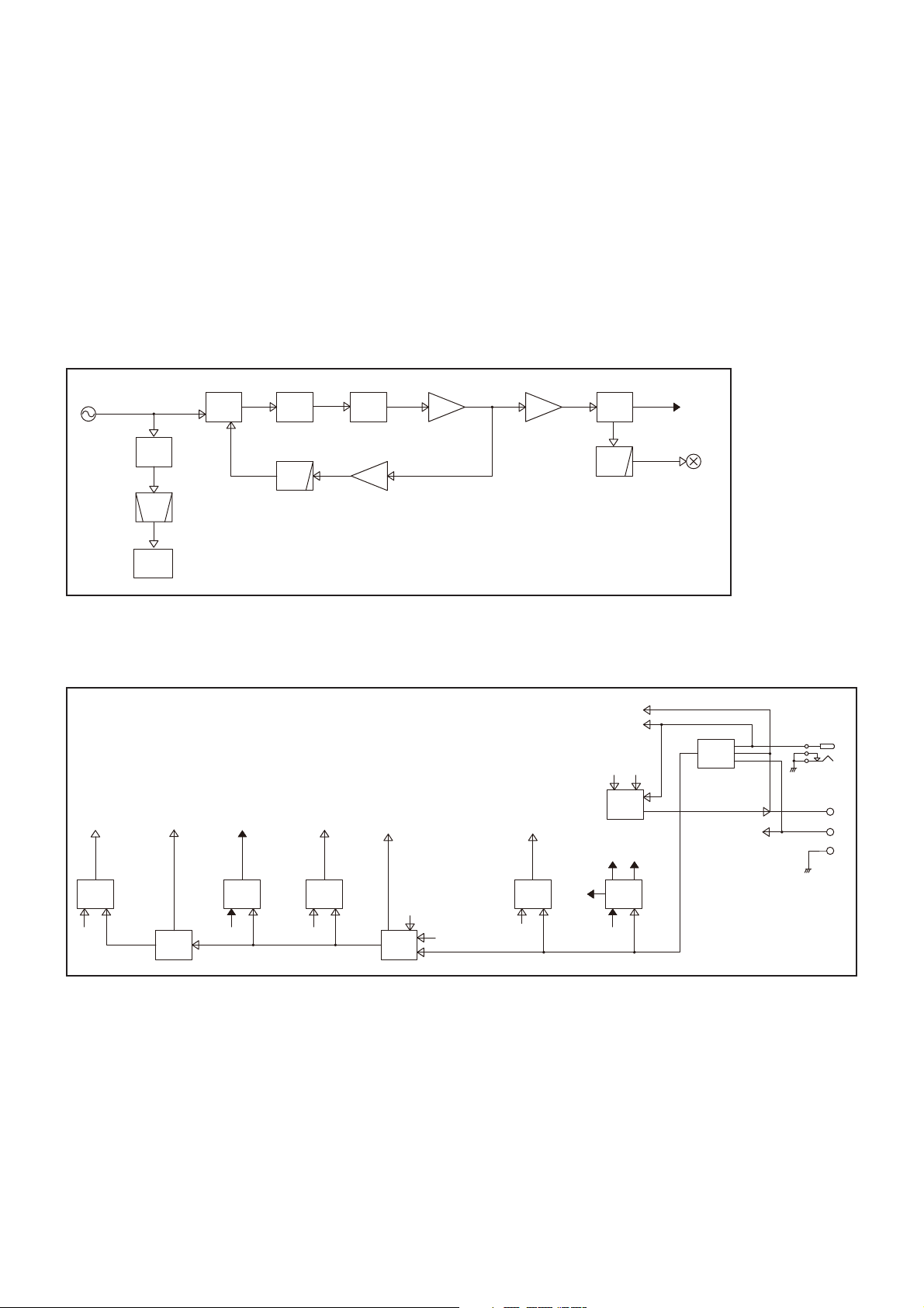
4-3 FREQUENCY SYNTHESIZER (MAIN UNIT)
• VCO
The ID-31A/E has a VCO (Q27, D10–D12) which generates
both the 1st LO signal and the TX signal. The output of buffer
(Q30) is amplifi ed by the LO AMP (Q32), and then used as
the TX/RX LO signal.
While receiving, the LO signal is applied to the 1st IF mixer (Q46), through the LO SW (D13) and LPF (L30, C280,
C289).
While transmitting, the LO signal is applied to the TX AMP circuits, through the LO SW (D14), buffer (Q48) and attenuator
(D20, D21).
• FREQUENCY SYNTHESIZER CIRCUITS
• PLL
A portion of VCO output signal is passed through two buffers
(Q29 and Q30) and LPF (L7, C137–C139, C144), and then
fed back to the PLL IC (IC6, pin 8).
The PLL IC (IC6) phase-compares the output of reference
frequency oscillator (TCXO; X1) and VCO, and the phasedifference is output as the charge pump current. The current
is passed though the loop fi lter (R67, R71, R90, R93, C74,
C91, C92, C96, C102) to be converted into the lock voltage,
which controls the oscillating frequency of VCO.
When the oscillation frequency drifts, its phase changes from
that of the reference frequency, causing a lock voltage change
to compensate for the drift in the VCO oscillating frequency.
X1
15.3MHz
Q38
IC13
REF
X3
45.9MHz
BPF
FM
DET
IC6
PLL
IC
FIN
LOOP
FILTER
LPF
VCO
Q27,D10,D11,D12
BUFF
Q29
BUFF
Q30
LO
AMP
Q32
LO
SW
D13,D14
LPF
1st LO
1st IF mixer
TX AMPs
Q46
4-4 VOLTAGE DIAGRAM
Voltage from the power supply is routed throughout the transceiver, through regulators and switches.
BTVIN
HV
VCC
CHGC
CHGH
CHG
T3C_INV
CTRL
Q6,Q7,Q9,Q10
D2,D5,D6
VCC-I
TXI-V
IC5,D9
CURRENT
DETECT
T3C
Q17,Q19
VCC
RX circuits
R3
R3
REG
Q24
R3C
Common circuits
3VS
3VS
REG
IC10
TX circuits AF power AMP
3VS
SP
REG
BTL5V
Q15,Q16
YGR
REG
T3C_INV
T5
Q37,D17
VCO, reference
frequency oscillator,etc.
PS3
PCON
SW
REG
IC4
Common circuits
5VS
+5V
REG
+5V
IC15
DC
SW
IC1,
Q1,Q2,Q3,Q8,
D1,D3,D4
CHG
BTDET
J2
+
S
-
4 - 3
 Loading...